


56F8356/56F8156
Data Sheet
Preliminary Technical Data
56F8300
16-bit Digital Signal Controllers
MC56F8356
Rev. 10.0
12/2005
freescale.com

Document Revision History
Version History Description of Change
Rev 1.0
Rev 2.0
Rev 3.0
Rev 4.0
Rev 5.0
Rev 6.0
Rev 7.0 Added 56F8156 information; edited to indicate differences in 56F8356 and 56F8 156. Refor-
Rev 8.0 Added output voltage maximum value and note to clarify in Table 10-1; also removed overall
Rev 9.0 Updated Table 10-24 to reflect new value for maximum Uncalibrated Gain Error
Rev 10.0 Deleted RSTO from Pin Group 2 (listed after Table 10-1). Deleted formula for Max Ambient
Initial Public Release
Added Package Pins to GPIO Table in Part 8 General Purpose Input/Output (GPIO). Added
“Typical Min” values to Table 10-18. Editing grammar, spelling, consistency of language
throughout family. Updated values in Regulator Parameters Table 10-9, External Clock
Operation Timing Requirements Table 10-13, SPI Timing Table 10-18, ADC Parameters
Table 10-24, and IO Loading Coefficients at 10MHz Table 10-25.
Added Part 4.8, added the word “access” to FM Error Interrupt in Table 4-5, documenting only
Typ. numbers for LVI in Table 10-6, updated EMI numbers and writeup in Part 10.8.
Updated numbers in Table 10-7 and Table 10-8 with more recent data, Corrected typo in
Table 10-3 in Pd characteristics.
Replace any reference to Flash Interface Unit with Flash Memory Module; corrected thermal
numbers for 144 LQFP in Table 10-3; removed unneccessary notes in Table 10-12; corrected
temperature range in Table 10-14; added ADC calibration information to Table 10-24 and new
graphs in Figure 10-22
Adding/clarifing notes to Table 4-4 to help clarify independen t program flash blocks and other
Program Flash modes, clarification to Table 1 0-23, corrected Digital Input Current Low (pull-up
enabled) numbers in
Table 10-1.
matted for Freescale look and feel. Updated Temperature Sensor and ADC tables, then
updated balance of electrical tables for consistency throughout family. Clarified I/O power
description in Table 2-2, added note to Table 10-7 and clarified Section 12.3.
life expectancy note, since life expectancy is dependent on customer usage and must be
determined by reliability engineering. Clarified value and unit measure for Maximum allowed
in Table 10-3. Corrected note about average value for Flash Data Retention in Table 10-4.
P
D
Added new RoHS-compliant orderable part numbers in Table 13-1.
Operating Temperature (Automotive) and Max Ambient Operating Temperature (Industrial) in
Table 10-4. Added RoHS-compliance and “pb-free” language to back cover.
Table 10-5. Removed text and Table 10-2; replaced with note to
Please see http://www.freescale.com for the most current Data Sheet revision.
56F8356 Technical Data, Rev. 10.0
2 Freescale Semiconductor
Preliminary
56F8356/56F8156 General Description
Note: Features in italics are NOT available in the 56F8156 device.
• Up to 60 MIPS at 60MHz core frequency
• DSP and MCU functionality in a unified,
C-efficient architecture
• Access up to 1MB of off-chip program and data memory
• Chip Select Logic for glueless interface to ROM and
SRAM
• 256KB of Program Flash
• 4KB of Program RAM
• 8KB of Data Flash
• 16KB of Data RAM
• 16KB of Boot Flash
• Up to two 6-channel PWM modules
• Four 4-channel, 12-bit ADCs
EMI_MODE
6
3
3
6
3
4
4
4
5
4
4
TEMP_SENSE
4
4
1
2
2
PWM Outputs
Current Sense Inputs
or GPIOC
Fault Inputs
PWM Outputs
Current Sense Inputs
or GPIOD
Fault Inputs
AD0
ADCA
AD1
VREF
ADCB
Program Memory
128K x 16 Flash
Data Memory
4K x 16 Flash
8K x 16 RAM
Decoding
Peripherals
AD0
AD1
Quadrature
Decoder 0 or
Quad
Timer A or
GPIOC
Quadrature
Decoder 1 or
Quad
Timer B or
SPI1 or
GPIOC
Quad
Timer C o r
GPIOE
Quad
Timer D or
GPIOE
FlexCAN
PWMA
PWMB
Memory
2K x 16 RAM
8K x 16 Boot
Flash
SPI0 or
GPIOE
4
RSTO
Hardware Looping Unit
SCI1 or
GPIOD
2
EXTBOOT
RESET
Program Controller
and
XDB2
XAB1
XAB2
PAB
PDB
CDBR
CDBW
Peripheral
Device Selects
SCI0 or
GPIOE
2
5
JTAG/
EOnCE
Port
Address
Generation Unit
PAB
PDB
CDBR
CDBW
IPBus Bridge (IPBB)
RW
Control
COP/
Watchdog
IRQA
• Temperature Sensor
• Up to two Quadrature Decoders
• Optional on-chip regulator
• FlexCAN module
• Two Serial Communication Interfaces (SCIs)
• Up to two Serial Peripheral Interfaces (SPIs)
• Up to four general-purpose Quad Timers
• Computer Operating Properly (COP) / Watchdog
• JTAG/Enhanced On-Chip Emulation (OnCE™) for
unobtrusive, real-time debugging
• Up to 62 GPIO lines
• 144-pin LQFP Package
OCR_DIS
V
V
PP
2
56800E Core
IPAB IPWDB IPRDB
Interrupt
Controller
IRQB
V
CAP
DD
47
Digital Reg
16-Bit
Data ALU
16 x 16 + 36 -> 36-Bit MAC
Three 16-bit Input Registers
Four 36-bit Accumulators
System Bus
Control
System
Integration
Module
V
ss
5
Analog Reg
Low Voltage
Supervisor
R/W Control
Clock
resets
P
O
R
CLKO
V
DDA
2
Manipulation
Address Bus
External Data
Bus Switch
External Bus
Interface Unit
Bus Control
PLL
Clock
Generator
CLKMODE
V
SSA
Bit
Unit
External
Switch
O
S
C
6
2
8
7
9
2
XTAL
EXTAL
A0-5 or GPIOA8-13
A6-7 or GPIOE2-3
A8-15 or GPIOA0-7
GPIOB0 or A16
D0-6 or GPIOF9-15
D7-15 or GPIOF0-8
WR
RD
GPIOD0-1 or CS2-3
PS or CS0 or GPIOD8
or CS1 or GPIOD9
DS
56F8356 / 56F8156 Block Diagram
56F8356 Technical Data, Rev. 10.0
Freescale Semiconductor 3
Preliminary

Table of Contents
Part 1: Overview . . . . . . . . . . . . . . . . . . . . . . .5
1.1. 56F8356/56F8156 Features . . . . . . . . . . . . . 5
1.2. Device Description . . . . . . . . . . . . . . . . . . . . 7
1.3. Award-Winning Development Environment . 9
1.4. Architecture Block Diagram . . . . . . . . . . . . 10
1.5. Product Documentation . . . . . . . . . . . . . . . 14
1.6. Data Sheet Conventions . . . . . . . . . . . . . . 14
Part 2: Signal/Connection Descriptions . . .15
2.1. Introduction . . . . . . . . . . . . . . . . . . . . . . . . . 15
2.2. Signal Pins . . . . . . . . . . . . . . . . . . . . . . . . . 18
Part 3: On-Chip Clock Synthesis (OCCS) . .37
3.1. Introduction . . . . . . . . . . . . . . . . . . . . . . . . . 37
3.2. External Clock Operation . . . . . . . . . . . . . . 37
3.3. Registers . . . . . . . . . . . . . . . . . . . . . . . . . . 39
Part 4: Memory Map . . . . . . . . . . . . . . . . . . .39
4.1. Introduction . . . . . . . . . . . . . . . . . . . . . . . . . 39
4.2. Program Map . . . . . . . . . . . . . . . . . . . . . . . 40
4.3. Interrupt Vector Table . . . . . . . . . . . . . . . . . 42
4.4. Data Map . . . . . . . . . . . . . . . . . . . . . . . . . . 46
4.5. Flash Memory Map . . . . . . . . . . . . . . . . . . . 46
4.6. EOnCE Memory Map . . . . . . . . . . . . . . . . . 48
4.7. Peripheral Memory Mapped Registers . . . . 49
4.8. Factory Programmed Memory . . . . . . . . . . 76
Part 5: Interrupt Controller (ITCN) . . . . . . . .77
5.1. Introduction . . . . . . . . . . . . . . . . . . . . . . . . . 77
5.2. Features . . . . . . . . . . . . . . . . . . . . . . . . . . . 77
5.3. Functional Description . . . . . . . . . . . . . . . . 77
5.4. Block Diagram . . . . . . . . . . . . . . . . . . . . . . 79
5.5. Operating Modes . . . . . . . . . . . . . . . . . . . . 79
5.6. Register Descriptions . . . . . . . . . . . . . . . . . 80
5.7. Resets . . . . . . . . . . . . . . . . . . . . . . . . . . . 106
Part 6: System Integration Module (SIM) .107
6.1. Overview . . . . . . . . . . . . . . . . . . . . . . . . . 107
6.2. Features . . . . . . . . . . . . . . . . . . . . . . . . . . 107
6.3. Operating Modes . . . . . . . . . . . . . . . . . . . 108
6.4. Operating Mode Register . . . . . . . . . . . . . 108
6.5. Register Descriptions . . . . . . . . . . . . . . . . 109
6.6. Clock Generation Overview . . . . . . . . . . . 122
6.7. Power-Down Modes Overview . . . . . . . . . 123
6.8. Stop and Wait Mode Disable Func tion . . . 123
6.9. Resets . . . . . . . . . . . . . . . . . . . . . . . . . . . 124
Part 8: General Purpose Input/Output
(GPIO) . . . . . . . . . . . . . . . . . . . . . . 127
8.1. Introduction . . . . . . . . . . . . . . . . . . . . . . . .127
8.2. Memory Maps . . . . . . . . . . . . . . . . . . . . . .128
8.3. Configuration . . . . . . . . . . . . . . . . . . . . . . .128
Part 9: Joint Test Action Group (JTAG) . 133
9.1. 56F8356 Information . . . . . . . . . . . . . . . . .133
Part 10: Specifications . . . . . . . . . . . . . . . 134
10.1. General Characteristics . . . . . . . . . . . . . .134
10.2. DC Electrical Characteristics . . . . . . . . . .138
10.3. AC Electrical Characteristics . . . . . . . . . .142
10.4. Flash Memory Characteristics . . . . . . . . .142
10.5. External Clock Operation Timing . . . . . . .143
10.6. Phase Locked Loop Timing . . . . . . . . . . .143
10.7. Crystal Oscillator Timing . . . . . . . . . . . . .144
10.8. External Memory Interface Timing . . . . . .144
10.9. Reset, Stop, Wait, Mode Select, and
Interrupt Timing . . . . . . . . . . . . . .147
10.10. Serial Peripheral Interface (SPI) Timing .149
10.11. Quad Timer Timing . . . . . . . . . . . . . . . .153
10.12. Quadrature Decoder Timing . . . . . . . . . .153
10.13. Serial Communication Interface (SCI)
Timing . . . . . . . . . . . . . . . . . . . . .154
10.14. Controller Area Network (CAN) Timing .155
10.15. JTAG Timing . . . . . . . . . . . . . . . . . . . . .155
10.16. Analog-to-Digital Converter (ADC)
Parameters . . . . . . . . . . . . . . . . .157
10.17. Equivalent Circuit for ADC Inputs . . . . . .160
10.18. Power Consumption . . . . . . . . . . . . . . . .160
Part 11: Packaging . . . . . . . . . . . . . . . . . . 162
11.1. 56F8356 Package and Pin-Out
Information . . . . . . . . . . . . . . . . . .162
11.2. 56F8156 Package and Pin-Out
Information . . . . . . . . . . . . . . . . . .165
Part 12: Design Considerations . . . . . . . . 169
12.1. Thermal Design Considerations . . . . . . . .169
12.2. Electrical Design Considerations . . . . . . .170
12.3. Power Distribution and I/O Ring
Implementation . . . . . . . . . . . . . .171
Part 13: Ordering Information . . . . . . . . . 172
Part 7: Security Features . . . . . . . . . . . . . .124
7.1. Operat ion with Security Enabled . . . . . . . 124
7.2. Flash Access Blocking Mechanisms . . . . 125
56F8356 Technical Data, Rev. 10.0
4 Freescale Semiconductor
Preliminary

Part 1 Overview
1.1 56F8356/56F8156 Features
1.1.1 Core
• Efficient 16-bit 56800E family controller engine with dual Harvard architecture
• Up to 60 Million Instructions Per Second (MIPS) at 60MHz core frequency
• Single-cycle 16 × 16-bit parallel Multiplier-Accumulator (MAC)
• Four 36-bit accumulators, including extension bits
• Arithmetic and logic multi-bit shifter
• Parallel instruction set with unique DSP addressing modes
• Hardware DO and REP loops
• Three internal address buses
• Four internal data buses
• Instruction set supports both DSP and controller functions
• Controller style addressing modes and instructions for compact code
• Efficient C compiler and local variable support
• Software subroutine and interrupt stack with depth limited only by memory
• JTAG/EOnCE debug programming interface
56F8356/56F8156 Features
1.1.2 Differences Between Devices
Table 1-1 outlines the key differences between the 56F8356 and 56F8156 devices.
Table 1-1 Device Differences
Feature 56F8356 56F8156
Guaranteed Speed 60MHz/60 MIPS 40MHz/40 MIPS
Program RAM 4KB Not Available
Data Flash 8KB Not Available
PWM 2 x 6 1 x 6
CAN 1 Not Available
Quad Timer 4 2
Quadrature Decoder 2 x 4 1 x 4
Temperature Sensor 1 Not Available
Dedicated GPIO — 5
56F8356 Technical Data, Rev. 10.0
Freescale Semiconductor 5
Preliminary

1.1.3 Memory
Note: Features in italics ae NOT available in the 56F8156 device.
• Harvard architecture permits as many as three simultaneous accesses to program and data memory
• Flash security protection feature
• On-chip memory, including a low-cost, high-volume Flash solution
— 256KB of Program Flash
— 4KB of Program RAM
— 8KB of Data Flash
— 16KB of Data RAM
— 16KB of Boot Flash
• Off-chip memory expansion capabilities programmable for 0 - 30 wait states
— Access up to 1MB of program memory or 1MB of data memory
— Chip select logic for glueless interface to ROM and SRAM
• EEPROM emulation capability
1.1.4 Peripheral Circuits
Note: Features in italics are NOT available in the 56F8156 device.
• Pulse Width Modulator:
— In the 56F8356, two Pulse W idth Modulator mod ules, each with six PWM out puts, three Current Sense
inputs, and three Fault inputs; fault-tolerant design with dead time insertion; supports both
center-aligned and edge-aligned modes
— In the 56F8156, one Pulse Width Modulator module with six PWM outputs, three Current Sense inputs,
and three Fault inputs; fault-tolerant design with dead time insertion; supports both center-aligned and
edge-aligned modes
• Four 12-bit, Analog-to-Digital Converters (ADCs), which support four simultane ous conversions with
quad, 4-pin multiplexed inputs; ADC and PWM modules can be synchronized through Timer C, channels
2 and 3
• Quadrature Decoder:
— In the 56F8356, two four-input Quadrature Decoders or two additional Quad Timers
— In the 56F8156, one four-input Quadrature Decoder, which works in conjunction with Quad Timer A
• Temperature Sensor can be connected, on the board, to any of the ADC inputs to monitor the on-chip
temperature
•Quad Timer:
— In the 56F8356, four dedicated general-purpose Quad Timers totaling three dedicated pins: Timer C
with one pin and Timer D with two pins
— In the 56F8156, two Quad Timers; Timer A and Timer C both work in conjunction with GPIO
• Optional on-chip regulator
• FlexCAN (CAN Version 2.0 B-compliant ) module with 2-pin port for transmit and receive
56F8356 Technical Data, Rev. 10.0
6 Freescale Semiconductor
Preliminary

Device Description
• Two Serial Communication Interfaces (SCIs), each with two pins (or four additional GPIO lines)
• Up to two Serial Peripheral Interfaces (SPIs), both with configurable 4-pin port (or eight additional GPIO
lines)
— In the 56F8356, SPI1 can also be used as Quadrature Decoder 1 or Quad Timer B
— In the 56F8156, SPI1 can alternately be used only as GPIO
• Computer Operating Properly (COP) / Watchdog timer
• Two dedicated external interrupt pins
• 62 General Purpose I/O (GPIO) pins
• External reset input pin for hardware reset
• External reset output pin for system reset
• Integrated low-voltage interrupt module
• JTAG/Enhanced On-Ch ip Emulation (OnCE) for unobtrusive, processor speed-independent, real-time
debugging
• Software-programmable, Phase Lock Loop (PLL)-based frequency synthesizer for the core clock
1.1.5 Energy Information
• Fabricated in high-density CMOS with 5V-tolerant, TTL-compatible digital inputs
• On-board 3.3V down to 2.6V voltage regulator for powering internal logic and memories; can be disabled
• On-chip regulators for digital and analog circuitry to lower cost and reduce noise
• Wait and Stop modes available
• ADC smart power management
• Each peripheral can be individually disabled to save power
1.2 Device Description
The 56F8356 and 56F8156 are members of the 56800E core-based family of controllers. Each combines,
on a single chip, the processing power of a Digital Signal Processor (DSP) and the functionality of a
microcontroller with a flexible set of peripherals to create an extremely cost-effective solution. Because
of its low cost, configuration flexibility, and compact program code, the 56F8356 and 56F8156 are
well-suited for many applications. The devices include many peripherals that are especially useful for
motion control, smart appliances, steppers, encoders, tachometers, limit switches, power supply and
control, automotive control (56F8156 only), engine management, noise suppression, remote utility
metering, industrial control for power, lighting, and automation applications.
The 56800E core is based on a Harvard-style architecture consisting of three execution units operating in
parallel, allowing as many as six operations per instruction cycle. The MCU-style programming model and
optimized instruction set allow straightforward generation of efficient, compact DSP and control code.
The instruction set is also highly efficient for C/C++ Compilers to enable rapid development of optimized
control applications.
The 56F8356 and 56F8156 support program execution from either internal or external memories. Two
data operands can be accessed from the on-chip data RAM per instruction cycle. These devices also
provide two external dedicated interrupt lines and up to 62 General Purpose Input/Output (GPIO) lines,
depending on peripheral configuration.
56F8356 Technical Data, Rev. 10.0
Freescale Semiconductor 7
Preliminary

1.2.1 56F8356 Features
The 56F8356 controller includes 256KB of Program Flash and 8KB of Data Flash (each programmable
through the JTAG port) with 4KB of Program RAM and 16KB of Data RAM. It also supports program
execution from external memory.
A total of 16KB of Boot Flash is incorporated for easy customer inclusion of field-programmable software
routines that can be used to program the main Program and Data Flash memory areas. Both Program and
Data Flash memories can be independently bulk erased or erased in pages. Program Flash page erase size
is 1KB. Boot and Data Flash page erase size is 512 bytes. The Boot Flash memory can also be either bulk
or page erased.
A key application-specific feature of the 56F8356 is the inclusion of two Pulse Width Modulator (PWM)
modules. These modules each incorporate three complementary, individually programmable PWM signal
output pairs (each module is also capable of supporting six independent PWM functions, for a total of 12
PWM outputs) to enhance motor control functionality. Complementary operation permits programmable
dead time insertion, distortion correction via current sensing by software, and separate top and bottom
output polarity control. The up-counter value is programmable to support a continuously variable PWM
frequency. Edge-aligned and center-aligned synchronous pulse width control (0% to 100% modulation) is
supported. The device is capable of controlling most motor types: ACIM (AC Induction Motors); both
BDC and BLDC (Brush and Brushless DC motors); SRM and VRM (Switched and Variable Reluctance
Motors); and stepper motors. The PWMs incorporate fault protection and cycle-by-cycle current limiting
with sufficient output drive capability to directly drive standard optoisolators. A “smoke-inhibit”,
write-once protection feature for key parameters is also included. A patented PWM waveform distortion
correction circuit is also provided. Each PWM is double-buffered and includes interrupt controls to permit
integral reload rates to be programmable from 1 to 16. The PWM modules provide reference outputs to
synchronize the Analog-to-Digital Converters through two channels of Quad Timer C.
The 56F8356 incorporates two Quadrature Decoders capable of capturing all four transitions on the
two-phase inputs, permitting generation of a number proportional to actual position. Speed computation
capabilities accommodate both fast- and slow-moving shafts. An integrated watchdog timer in the
Quadrature Decoder can be programmed with a time-out value to alert when no shaft motion is detected.
Each input is filtered to ensure only true transitions are recorded.
This controller also provides a full set of standard programmable peripherals that include two Serial
Communications Interfaces (SCIs); two Serial Peripheral Interfaces (SPIs); and four Quad Timers. Any of
these interfaces can be used as General Purpose Input/Outputs (GPIOs) if that function is not required. A
Flex Controller Area Network (FlexCAN) interface (CAN Version 2.0 B-compliant) and an internal
interrupt controller are a part of the 56F8356.
1.2.2 56F8156 Features
The 56F8156 controller includes 256KB of Program Flash, programmable through the JTAG port, with
16KB of Data RAM. It also supports program execution from external memory.
A total of 16KB of Boot Flash is incorporated for easy customer inclusion of field-programmable software
routines that can be used to program the main Program Flash memory areas, which can be independently
bulk erased or erased in pages. Program Flash page erase size is 1KB. Boot Flash page erase size is 512
bytes. and the Boot Flash memory can also be either bulk or page erased.
56F8356 Technical Data, Rev. 10.0
8 Freescale Semiconductor
Preliminary

Award-Winning Development Environment
A key application-specific feature of the 56F8156 is the inclusion of one Pulse Width Modulator (PWM)
module. This module incorporates three complementary, individually programmable PWM signal output
pairs and can also support six independent PWM functions to enhance motor control functionality.
Complementary operation permits programmable dead time insertion, distortion correction via current
sensing by software, and separate top and bottom output polarity control. The up-counter value is
programmable to support a continuously variable PWM frequency. Edge-aligned and center-aligned
synchronous pulse width control (0% to 100% modulation) is supported. The device is capable of
controlling most motor types: ACIM (AC Induction Motors); both BDC and BLDC (Brush and Brushless
DC motors); SRM and VRM (Switched and Variable Reluctance Motors); and stepper motors. The PWM
incorporates fault protection and cycle-by-cycle current limiting with sufficient output drive capability to
directly drive standard optoisolators. A “smoke-inhibit”, write-once protection feature for key parameters
is also included. A patented PWM waveform distortion correction circuit is also provided. Each PWM is
double-buffered and includes interrupt controls to permit integral reload rates to be programmable from 1
to 16. The PWM module provides reference outputs to synchronize the Analog-to-Digital Converters
through two channels of Quad Timer C.
The 56F8156 incorporates a Quadrature Decoder capable of capturing all four transitions on the two-phase
inputs, permitting generation of a number proportional to actual position. Speed computation capabilities
accommodate both fast- and slow-moving shafts. An integrated watchdog timer in the Quadrature Decoder
can be programmed with a time-out value to alert when no shaft motion is detected. Each input is filtered
to ensure only true transitions are recorded.
This controller also provides a full set of standard programmable peripherals that include two Serial
Communications Interfaces (SCIs); two Serial Peripheral Interfaces (SPIs); and two Quad Timers. Any of
these interfaces can be used as General Purpose Input/Outputs (GPIOs) if that function is not required. An
internal interrupt controller are a part of the 56F8156.
1.3 Award-Winning Development Environment
Processor ExpertTM (PE) provides a Rapid Application Design (RAD) tool that combines easy-to-use
component-based software application creation with an expert knowledge system.
The CodeWarrior Integrated Development Environment is a sophisticated tool for code navigation,
compiling, and debugging. A complete set of evaluation modules (EVMs) and development system cards
will support concurrent engineering. Together, PE, CodeWarrior and EVMs create a complete, scalable
tools solution for easy, fast, and efficient development.
56F8356 Technical Data, Rev. 10.0
Freescale Semiconductor 9
Preliminary

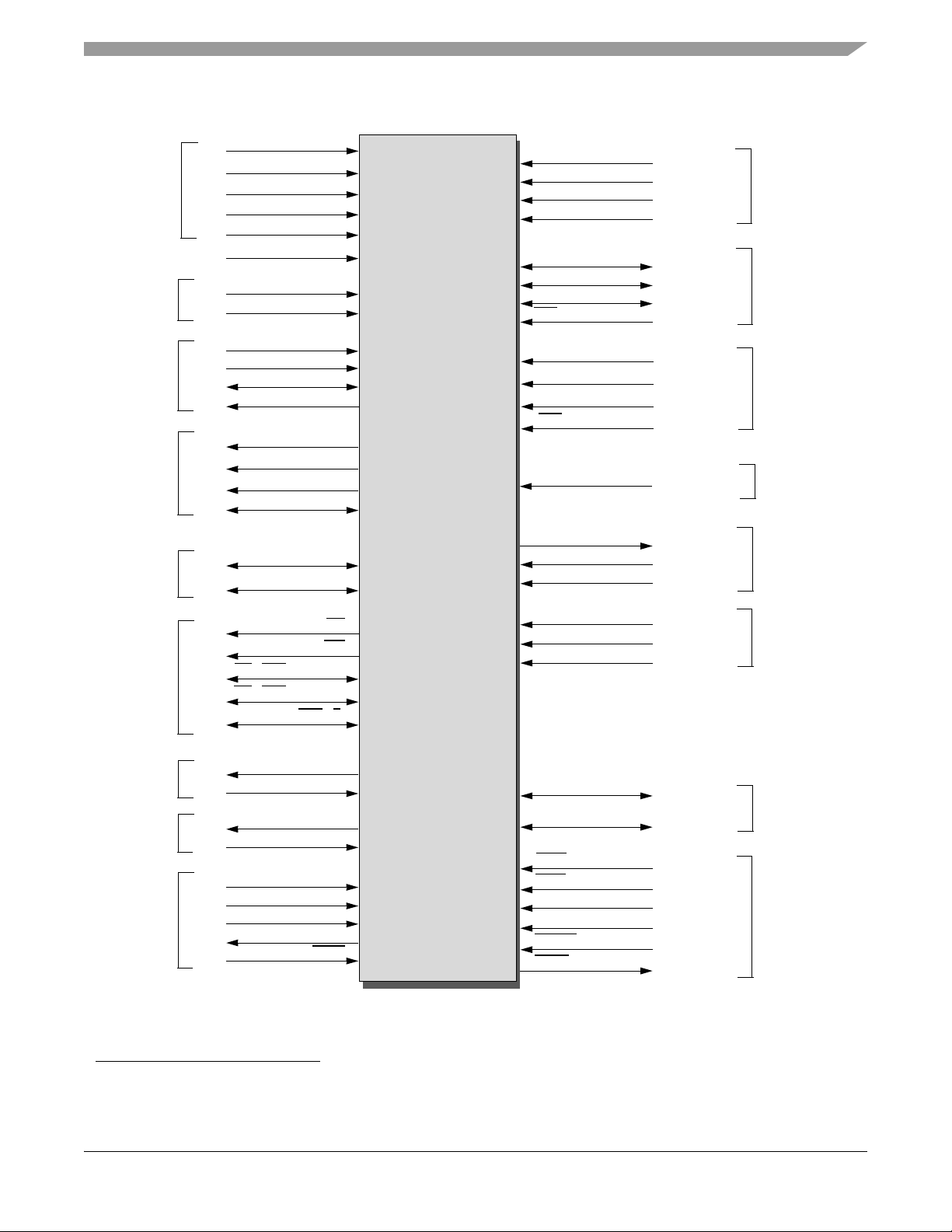
1.4 Architecture Block Diagram
Note: Features in italics are NOT available in the 56F8156 device and are shaded in the following figures.
The 56F8356/56F8156 architecture is shown in Figure 1-1 and Figure 1-2. Figure 1-1 illustrates how the
56800E system buses communicate with internal memories, the external memory interface and the IPBus
Bridge. Table 1-2 lists the internal buses in the 56800E architecture and provides a brief description of
their function. Figure 1-2 shows the peripherals and control blocks connected to the IPBus Bridge. The
figures do not show the on-board regulator and power and ground signals. They also do not show the
multiplexing between peripherals or the dedicated GPIOs. Please see Part 2, Signal/Connection
Descriptions, to see which signals are multiplexed with those of other peripherals.
Also shown in Figure 1-2 are connections between the PWM, Timer C and ADC blocks. These
connections allow the PWM and/or Timer C to control the timing of the start of ADC conversions. The
Timer C channel indicated can generate periodic start (SYNC) signals to the ADC to start its conversions.
In another operating mode, the PWM load interrupt (SYNC output) signal is routed internally to the Timer
C input channel as indicated. The timer can then be used to introduce a controllable delay before
generating its output signal. The timer output then triggers the ADC. To fully understand this interaction,
please see the 56F8300 Peripheral User Manual for clarification on the operation of all three of these
peripherals.
56F8356 Technical Data, Rev. 10.0
10 Freescale Semiconductor
Preliminary
Architecture Block Diagram
CHIP
TAP
Controller
TAP
Linking
5
JTAG / EOnCE
pdb_m[15:0]
pab[20:0]
cdbw[31:0]
Boot
Flash
Program
Flash
Program
RAM
56800E
xab1[23:0]
xab2[23:0]
EMI
Data RAM
17
16
6
Address
Data
Control
External
JTAG
Port
cdbr_m[31:0]
xdb2_m[15:0]
Data Flash
IPBus
To Flash
Control Logic
Bridge
Flash
Module
NOT available on the 56F8156 device.
IPBus
Figure 1-1 System Bus Interfaces
Note: Flash memories are encapsulated within the Flash Module(FM). Flash control is accomplished by the
I/O to the FM over the peripheral bus, while reads and writes are completed between the core and the
Flash memories.
Note: The primary data RAM port is 32 bits wide. Other data ports are 16 bits.
56F8356 Technical Data, Rev. 10.0
Freescale Semiconductor 11
Preliminary
To/From IPBus Bridge
CLKGEN
(OSC/PLL)
Interrupt
Controller
Low Voltage Interrupt
Timer A
POR & LVI
4
2
Quadrature Decoder 0
Timer D
Timer B
4
Quadrature Decoder 1
SPI 1
GPIOA
System POR
SIM
COP Reset
COP
FlexCAN
PWMA
PWMB
RESET
2
12
SYNC Output
13
GPIOB
GPIOC
GPIOD
GPIOE
GPIOF
4
2
2
SPI0
SCI0
SCI1
NOT available on the 56F8156 device.
Figure 1-2 Peripheral Subsystem
IPBus
SYNC Output
ch3i
Timer C
ch3o
ch2i
1
ch2o
8
ADCB
, V
1
REFP
8
, V
REFMID
ADCA
TEMP_SENSE
Note: ADCA and ADCB use the same voltage
reference circuit with V
, and V
V
REFN
REFLO
REFH
pins.
,
56F8356 Technical Data, Rev. 10.0
12 Freescale Semiconductor
Preliminary

Architecture Block Diagram
Table 1-2 Bus Signal Names
Name Function
Program Memory Interface
pdb_m[15:0] Program data bus for instruction word fetches or read operations.
cdbw[15:0] Primary core data bus used for program memory writes. (Only these 16 bits of the cdbw[31:0] bus
are used for writes to program memory.)
pab[20:0] Program memory address bus. Data is returned on pdb_m bus.
Primary Data Memory Interface Bus
cdbr_m[31:0] Pri mar y core data bus for memory reads. Addressed via xab1 bus.
cdbw[31:0] Primary core data bus for memory writes. Addressed via xab1 bus.
xab1[23:0]
Primary data address bus. Capable of addressing bytes
on cdbw and returned on cdbr_m. Also used to access memory-mapped I/O.
Secondary Data Memory Interface
xdb2_m[15:0] Secondary data bus used for secondary data address bus xab2 in the dual memory reads.
xab2[23:0] Secondary data address bus used for the second of two simultaneous accesses. Capable of
addressing only words. Data is returned on xdb2_m.
Peripheral Interface Bus
IPBus [15:0] Peripheral bus accesses all on-chip peripherals registers. This bus operates at the same clock rate
as the Primary Data Memory and therefore generates no delays when accessing the processor.
Write data is obtained from cdbw. Read data is provided to cdbr_m.
1. Byte accesses can only occur in the bottom half of the memory address space. The MSB of the address will be forced
to 0.
1
, words, and long data types. Data is written
56F8356 Technical Data, Rev. 10.0
Freescale Semiconductor 13
Preliminary

1.5 Product Documentation
The documents in Table 1-3 are required for a complete description and proper design with the
56F8356/56F8156 devices. Documentation is available from local Freescale distributors, Freescale
semiconductor sales offices, Freescale Literature Distribution Centers, or online at
http://www.freescale.com.
Table 1-3 Chip Documentation
Topic Description Order Number
DSP56800E
Reference Manual
56F8300 Peripheral
User Manual
56F8300 SCI/CAN
Bootloader User
Manual
56F8356/56F8156
Technical Data Sheet
Errata Details any chip issues that might be present MC56F8356E
Detailed description of the 56800E family architecture,
and 16-bit controller core processor and the instruction
set
Detailed description of peripherals of the 56F8300
devices
Detailed description of the SCI/CAN Bootloaders
56F8300 family of devices
Electrical and timing specifications, pin descriptions,
and package descriptions (this document)
DSP56800ERM
MC56F8300UM
MC56F83xxBLUM
MC56F8356
MC56F8156E
1.6 Data Sheet Conventions
This data sheet uses the following conventions:
OVERBAR
“asserted” A high true (active high) signal is high or a low true (active low) signal is low.
This is used to indicate a signal that is active when pulled low. For example, the RESET pin is
active when low.
“deasserted” A high true (active high) signal is low or a low true (active low) signal is high.
Examples: Signal/Symbol Logic State Signal State
PIN True Asserted VIL/V
PIN False Deasserted VIH/V
PIN True Asserted VIH/V
PIN False Deasserted VIL/V
1. Values for VIL, VOL, VIH, and VOH are defined by individual product specifications.
56F8356 Technical Data, Rev. 10.0
14 Freescale Semiconductor
Voltage
1
OL
OH
OH
OL
Preliminary

Introduction
Part 2 Signal/Connection Descriptions
2.1 Introduction
The input and output signals of the 56F8356 and 56F8156 are organized into functional groups, as detailed
in Table 2-1 and as illustrated in Figure 2-1. In Table 2-2, each table row describes the signal or signals
present on a pin.
Table 2-1 Functional Group Pin Allocations
Functional Group
Power (V
Power Option Control 1 1
Ground (VSS or V
Supply Capacitors1 & V
PLL and Clock 4 4
Address Bus 17 17
Data Bus 16 16
Bus Control 6 6
Interrupt and Program Control 6 6
Pulse Width Modulator (PWM) Ports 25 13
Serial Peripheral Interface (SPI) Port 0 4 4
Serial Peripheral Interface (SPI) Port 1 — 4
Quadrature Decoder Port 0
Quadrature Decoder Port 1
Serial Communications Interface (SCI) Ports 4 4
CAN Ports 2 —
Analog to Digital Converter (ADC) Ports 21 21
DD
or V
)99
DDA
)66
SSA
PP
2
3
Number of Pins in Package
56F8356 56F8156
66
44
4—
Quad Timer Module Ports 3 1
JTAG/Enhanced On-Chip Emulation (EOnCE) 5 5
Temperature Sense 1 —
Dedicated GPIO — 5
1. If the on-chip regulator is disabled, the V
2. Alternately, can function as Quad Timer pins or GPIO
3. Pins in this section can function as Quad Timer, SPI #1, or GPIO
Freescale Semiconductor 15
Preliminary
pins serve as 2.5V V
CAP
56F8356 Technical Data, Rev. 10.0
DD_CORE
power inputs
Power
Power
Power
Ground
Ground
Other
Supply
Ports
PLL
and
Clock
External
Address
Bus
or GPIO
V
DD_IO
V
DDA_ADC
V
DDA_OSC_PLL
V
SS
V
SSA_ADC
OCR_DIS
V
1 - V
CAP
CAP
V
1 & VPP2
PP
CLKMODE
EXTAL
XTAL
CLKO
A0 - A5 (GPIOA8 - 13)
A6 - A7 (GPIOE2 - 3)
A8 - A15 (GPIOA0 - 7)
GPIOB0 (A16)
7
PHASEA0 (TA0, GPIOC4)
1
1
5
1
1
56F8356
4
4
2
1
PHASEB0 (TA1, GPIOC5)
1
INDEX0 (TA2, GPIOC6)
1
HOME0 (TA3, GPIOC7)
1
SCLK0 (GPIOE4)
1
MOSI0 (GPIOE5)
1
MISO0 (GPIOE6)
1
1
SS0
(GPIOE7)
Quadrature
Decoder 0
or Quad
Timer A or
GPIO
SPI0 or
GPIO
1
1
1
1
PHASEA1(TB0, SCLK1, GPIOC0)
1
PHASEB1 (TB1, MOSI1, GPIOC1)
1
INDEX1 (TB2, MISO1, GPIOC2)
1
HOME1 (TB3, SS1
1
, GPIOC3)
Quadrature
Decoder 1 or
Quad Timer B
or SPI 1 or
GPIO
6
2
8
1
PWMA0 - 5
6
ISA0 - 2 (GPIOC8 - 10)
3
FAULTA0 - 2
3
PWMA or
GPIO
External
Data Bus
or GPIO
External
Bus
Control or
GPIO
SCI 0 or
GPIO
SCI 1
or GPIO
JTAG/
EOnCE
Port
D0 - D6 (GPIOF9 - 15)
D7 - D15 (GPIOF0 - 8)
RD
WR
PS / CS0 (GPIOD8)
DS / CS1 (GPIOD9)
GPIOD0 - 1 (CS2 - 3)
TXD0 (GPIOE0)
RXD0 (GPIOE1)
TXD1 (GPIOD6)
RXD1 (GPIOD7)
TCK
TMS
TDI
TDO
TRST
PWMB0 - 5
7
9
1
1
1
1
2
1
1
1
1
1
1
1
1
1
6
ISB0 - 2 (GPIOD10 - 12)
3
FAULTB0 - 3
4
ANA0 - 7
8
V
REF
5
ANB0 - 7
8
TEMP_SENSE
1
CAN_RX
1
CAN_TX
1
TC0 (GPIOE8)
1
TD0 - 1 (GPIOE10 - 11)
2
IRQA
1
IRQB
1
EXTBOOT
1
EMI_MODE
1
RESET
1
RSTO
1
PWMB or
GPIO
ADCA
ADCB
Temperature
Sensor
FlexCAN
QUAD
TIMER C and
D or GPIO
INTERRUPT/
PROGRAM
CONTROL
Figure 2-1 56F8356 Signals Identified by Functional Group1 (144-pin LQFP)
1. Alternate pin functionality is shown in parenthesis; pin direction/type shown is the default functionality.
56F8356 Technical Data, Rev. 10.0
16 Freescale Semiconductor
Preliminary
Power
Power
Power
Ground
Ground
Other
Supply
Ports
PLL
and
Clock
External
Address
Bus
or GPIO
V
DD_IO
V
DDA_ADC
V
DDA_OSC_PLL
V
SS
V
SSA_ADC
OCR_DIS
V
1 - V
CAP
V
PP
CAP
1 & VPP2
CLKMODE
EXTAL
XTAL
CLKO
A0 - A5 (GPIOA8 - 13)
A6 - A7 (GPIOE2 - 3)
A8 - A15 (GPIOA0 - 7)
GPIOB0 (A16)
Introduction
7
1
1
5
PHASEA0 (TA0, GPIOC4)
1
PHASEB0 (TA1, GPIOC5)
1
INDEX0 (TA2, GPIOC6)
1
HOME0 (TA3, GPIOC7)
1
Quadrature
Decoder 0
or Quad
Timer A or
GPIO
1
56F8356
1
4
4
2
1
1
1
1
SCLK0 (GPIOE4)
1
MOSI0 (GPIOE5)
1
MISO0 (GPIOE6)
1
SS0
1
(SCLK1, GPIOC0)
1
(MOSI1, GPIOC1)
1
(MISO1, GPIOC2)
1
(S
1
SPI0 or
GPIO
(GPIOE7)
SPI 1 or
GPIO
S1, GPIOC3)
6
2
8
3
(GPIOC8 - 10)
GPIO
1
External
Data Bus
or GPIO
External
Bus
Control or
GPIO
SCI 0 or
GPIO
SCI 1
or GPIO
JTAG/
EOnCE
Port
D0 - D6 (GPIOF9 - 15)
D7 - D15 (GPIOF0 - 8)
RD
WR
PS / CS0 (GPIOD8)
DS / CS1 (GPIOD9)
GPIOD0 - 1 (CS2 - 3)
TXD0 (GPIOE0)
RXD0 (GPIOE1)
TXD1 (GPIOD6)
RXD1 (GPIOD7)
TCK
TMS
TDI
TDO
TRST
PWMB0 - 5
6
ISB0 - 2 (GPIOD10 - 12)
7
9
1
1
3
4
8
5
8
FAULTB0 - 3
ANA0 - 7
V
REF
ANB0 - 7
PWMB or
GPIO
ADCA
ADCB
1
1
2
1
1
1
TC0 (GPIOE8)
1
TD0 - 1 (GPIOE10 - 11)
2
QUAD
TIMER C or
GPIO
1
IRQA
1
1
1
1
1
1
1
1
1
1
1
IRQB
EXTBOOT
EMI_MODE
RESET
RSTO
INTERRUPT/
PROGRAM
CONTROL
Figure 2-2 56F8156 Signals Identified by Functional Group1 (144-pin LQFP)
1. Alternate pin functionality is shown in parenthesis; pin direction/type shown is the default functionality.
56F8356 Technical Data, Rev. 10.0
Freescale Semiconductor 17
Preliminary

2.2 Signal Pins
After reset, each pin is configured for its primary function (listed first). Any alternate functionality must
be programmed.
If the “State During Reset” lists more than one state for a pin, the first state is the actual reset state. Other
states show the reset condition of the alternate function, which you get if the alternate pin function is
selected without changing the configuration of the alternate peripheral. For example, the A8/GPIOA0 pin
shows that it is tri-stated during reset. If the GPIOA_PER is changed to select the GPIO function of the
pin, it will become an input if no other registers are changed.
Table 2-2 Signal and Package Information for the 144-Pin LQFP
State
Signal Name Pin No. Type
During
Reset
Signal Description
V
DD_IO
V
DD_IO
V
DD_IO
V
DD_IO
V
DD_IO
V
DD_IO
V
DD_IO
V
DDA_ADC
V
DDA_OSC_PLL
V
SS
V
SS
V
SS
1 Supply I/O Power — This pin supplies 3.3V power to the chip I/O interface
and also the Processor core throught the on-chip voltage
16
31
38
66
84
119
102 Supply ADC Power — This pin supplies 3.3V power to the ADC modules.
80 Supply Oscillator and PLL Power — This pin supplies 3.3V power to the
27 Supply V
37
63
regulator, if it is enabled.
It must be connected to a clean analog power supply.
OSC and to the internal regulator that in turn supplies the Phase
Locked Loop. It must be connected to a clean analog power
supply.
— These pins provide ground for chip logic and I/O drivers.
SS
V
SS
V
SS
V
SSA_ADC
18 Freescale Semiconductor
69
144
103 Supply ADC Analog Ground — This pin supplies an analog ground to the
ADC modules.
56F8356 Technical Data, Rev. 10.0
Preliminary

Table 2-2 Signal and Package Information for the 144-Pin LQFP
State
Signal Name Pin No. Type
OCR_DIS 79 Input Input On-Chip Regulator Disab le —
During
Reset
Signal Description
Tie this pin to V
Tie this pin to V
to enable the on-chip regulator
SS
to disable the on-chip regulator
DD
This pin is intended to be a static DC signal from power-up to
shut down. Do not try to toggle this pin for power savings
during operation.
Signal Pins
1 51 Supply Supply V
V
CAP
1 - 4 — When OCR_DIS is tied to VSS (regulator enabled),
CAP
connect each pin to a 2.2µF or greater bypass capacitor in order to
2 128
V
CAP
3 83
V
CAP
4 15
V
CAP
1 125 Input Input VPP1 - 2 — These pins should be left unconnected as an open
V
PP
bypass the core logic voltage regulator, required for proper chip
operation. When OCR_DIS is tied to V
these pins become V
DD_CORE
and should be connected to a
(regulator disabled),
DD
regulated 2.5V power supply.
circuit for normal functionality.
VPP2 2
CLKMODE 87 Input Input Clock Input Mode Selection — This input determines the
function of the XTAL and EXTAL pins.
1 = External clock input on XTAL is used to directly drive the input
clock of the chip. The EXTAL pin should be grounded.
0 = A crystal or ceramic resonator should be connected between
XTAL and EXTAL.
EXTAL 82 Input Input External Crystal Oscillator Input — This input can be connected
to an 8MHz external crystal. Tie this pin low if XTAL is driven by an
external clock source.
XTAL 81 Input/
Output
Chip-driven Crystal Oscillator Output — This output connects the internal
crystal oscillator output to an external crystal.
If an external clock is used, XTAL must be used as the input and
EXTAL connected to GND.
The input clock can be selected to provide the clock directly to the
core. This input clock can also be selected as the input clock for
the on-chip PLL.
CLKO 3 Output Tri-Stated Clock Output — This pin outputs a buffered clock signal. Using
the SIM CLKO Select Register (SIM_CLKOSR), this pin can be
programmed as any of the following: disabled, CLK_MSTR
(system clock), IPBus clock, oscillator output, prescaler clock and
postscaler clock. Other signals are also available for test
purposes.
See Part 6.5.7 for details.
56F8356 Technical Data, Rev. 10.0
Freescale Semiconductor 19
Preliminary

Table 2-2 Signal and Package Information for the 144-Pin LQFP
Signal Name Pin No. Type
State
During
Reset
Signal Description
A0
(GPIOA8)
A1
(GPIOA9)
A2
(GPIOA10)
A3
(GPIOA11)
A4
(GPIOA12)
A5
(GPIOA13)
A6
138 Output
Input/
Output
10
11
12
13
14
17 Output
Tri-stated Address Bus — A0 - A5 specify six of the address lines for
external program or data memory accesses.
Depending upon the state of the DRV bit in the EMI bus control
register (BCR), A0 - A5 and EMI control signals are tri-stated when
the external bus is inactive.
Most designs will want to change the DRV state to DRV = 1 instead of
using the default setting.
Port A GPIO — These six GPIO pins can be individually
programmed as input or output pins.
After reset, the default state is Address Bus.
To deactivate the internal pull-up resistor, clear the appropriate
GPIO bit in the GPIOA_PUR register.
Example: GPIOA8, clear bit 8 in the GPIOA_PUR register.
Tri-stated
Address Bus — A6 - A7 specify two of the address lines for
external program or data memory accesses.
Depending upon the state of the DRV bit in the EMI bus control
register (BCR), A6 - A7 and EMI control signals are tri-stated when
the external bus is inactive.
Most designs will want to change the DRV state to DRV = 1 instead of
using the default setting.
(GPIOE2)
A7
(GPIOE3)
20 Freescale Semiconductor
18
Schmitt
Input/
Output
Input
56F8356 Technical Data, Rev. 10.0
Port E GPIO — These two GPIO pins can be individually
programmed as input or output pins.
After reset, the default state is Address Bus.
To deactivate the internal pull-up resistor, clear the appropriate
GPIO bit in the GPIOE_PUR register.
Example: GPIOE2, clear bit 2 in the GPIOE_PUR register.
Preliminary

Table 2-2 Signal and Package Information for the 144-Pin LQFP
Signal Name Pin No. Type
State
During
Reset
Signal Pins
Signal Description
A8
(GPIOA0)
A9
(GPIOA1)
A10
(GPIOA2)
A11
(GPIOA3)
A12
(GPIOA4)
A13
(GPIOA5)
A14
(GPIOA6)
19 Output
Schmitt
20
21
22
23
24
25
Input/
Output
Tri-stated
Input
Address Bus— A8 - A15 specify eight of the address lines for
external program or data memory accesses.
Depending upon the state of the DRV bit in the EMI bus control
register (BCR), A8 - A15 and EMI control signals are tri-stated when
the external bus is inactive.
Most designs will want to change the DRV state to DRV = 1 instead of
using the default setting.
Port A GPIO — These eight GPIO pins can be individually
programmed as input or output pins.
After reset, the default state is Address Bus.
To deactivate the internal pull-up resistor, clear the appropriate
GPIO bit in the GPIOA_PUR register.
Example: GPIOA0, clear bit 0 in the GPIOA_PUR register.
A15
(GPIOA7)
Freescale Semiconductor 21
Preliminary
26
56F8356 Technical Data, Rev. 10.0

Table 2-2 Signal and Package Information for the 144-Pin LQFP
Signal Name Pin No. Type
State
During
Reset
Signal Description
GPIOB0
(A16)
D0
33 Schmitt
Input/
Output
Output
59 Input/
Output
Input
Tri-stated
Tri-stated
Port B GPIO — This GPIO pin can be programmed as an input or
output pin.
Address Bus — A16 specifies one of the address lines for
external program or data memory accesses. Depending upon the
state of the DRV bit in the EMI bus control register (BCR), A16 and
EMI control signals are tri-stated when the external bus is inactive.
Most designs will want to change the DRV state to DRV = 1 instead of
using the default setting.
After reset, the start-up state of GPIOB0 (GPIO or address) is
determined as a function of EXTBOOT, EMI_MODE and the Flash
security setting. See Table 4-4 for further information on when this
pin is configured as an address pin at reset. In all cases, this state
may be changed by writing to GPIOB_PER.
To deactivate the internal pull-up resistor, clear bit 0 in the
GPIOB_PUR register.
Data Bus — D0 - D6 specify part of the data for external program or
data memory accesses.
Depending upon the state of the DRV bit in the EMI bus control
register (BCR), D0 - D6 are tri-stated when the external bus is
inactive.
(GPIOF9)
D1
(GPIOF10)
D2
(GPIOF11)
D3
(GPIOF12)
D4
(GPIOF13)
D5
(GPIOF14)
D6
(GPIOF15)
60
72
75
76
77
78
Input/
Output
Most designs will want to change the DRV state to DRV = 1 instead of
using the default setting.
Input
56F8356 Technical Data, Rev. 10.0
Port F GPIO — These seven GPIO pins can be individually
programmed as input or output pins.
At reset, these pins default to the EMI Data Bus function.
To deactivate the internal pull-up resistor, clear the appropriate
GPIO bit in the GPIOF_PUR register.
Example: GPIOF9, clear bit 9 in the GPIOF_PUR reg i ste r.
22 Freescale Semiconductor
Preliminary

Table 2-2 Signal and Package Information for the 144-Pin LQFP
Signal Name Pin No. Type
State
During
Reset
Signal Pins
Signal Description
D7
(GPIOF0)
D8
(GPIOF1)
D9
(GPIOF2)
D10
(GPIOF3)
D11
(GPIOF4)
D12
(GPIOF5)
D13
(GPIOF6)
D14
(GPIOF7)
28 Input/
Output
Input/
Output
29
30
32
133
134
135
136
Tri-stated
Input
Data Bus — D7 - D14 specify part of the data for external program
or data memory accesses.
Most designs will want to change the DRV state to DRV = 1 instead of
using the default setting.
Port F GPIO — These eight GPIO pins can be individually
programmed as input or output pins.
At reset, these pins default to Data Bus functionality.
To deactivate the internal pull-up resistor, clear the appropriate
GPIO bit in the GPIOF_PUR register.
Example: GPIOF0, clear bit 0 in the GPIOF_PUR reg i ste r.
D15
(GPIOF8)
137 Input/
Output
Input/
Output
Tri-stated
Input
56F8356 Technical Data, Rev. 10.0
Data Bus — D15 specifies part of the data for external program or
data memory accesses.
Most designs will want to change the DRV state to DRV = 1 instead of
using the default setting.
Port F GPIO — This GPIO pin can be individually programmed as
an input or output pin.
At reset, this pin defaults to the Data Bus function.
To deactivate the internal pull-up resistor, clear bit 8 in the
GPIOF_PUR register.
Freescale Semiconductor 23
Preliminary

Table 2-2 Signal and Package Information for the 144-Pin LQFP
State
Signal Name Pin No. Type
RD 45 Output Tri-stated Read Enable — RD is asserted during external memory read
During
Reset
Signal Description
cycles. When RD
and an external device is enabled onto the data bus. When RD
deasserted high, the external data is latched inside the device.
When RD is asserted, it qualifies the A0 - A16, PS, DS, and CSn
pins. RD
or ROM.
Depending upon the state of the DRV bit in the EMI bus control
register (BCR ) , RD is
Most designs will want to change the DRV state to DRV = 1 instead of
using the default setting.
To deactivate the internal pull-up resistor, set the CTRL bit in the
SIM_PUDR register.
can be connected directly to the OE pin of a Static RAM
is asserted low, pins D0 - D15 become inputs
tri-stated when the external bus is inactive.
is
WR
PS
(CS0)
44 Output Tri-stated Write Enable — WR is asserted during external memory write
is asserted low, pins D0 - D15 become outputs
, DS, and CSn pins. WR can
is tri-stated when the external bus is inactive.
in the
signal. PS is asserted low for external program
is tri-stated when the external bus is inactive.
46 Output
Tri-stated
cycles. When WR
and the device puts data on the bus. When WR is deasserted high,
the external data is latched inside the external device. When WR is
asserted, it qualifies the A0 - A16, PS
be connected directly to the WE pin of a static RAM.
Depending upon the state of the DRV bit in the EMI bus control
register (BCR), WR
Most designs will want to change the DRV state to DRV = 1 instead of
using the default setting.
To deactivate the internal pull-up resistor, set the CTRL bit in the
SIM_PUDR register.
Program Memory Select — This signal is actually CS0
EMI, which is programmed at reset for compatibility with the
56F80x PS
memory access.
Depending upon the state of the DRV bit in the EMI bus control
register (BCR), CS0
resets to provide the PS function as defined on the 56F80x
CS0
devices.
(GPIOD8)
24 Freescale Semiconductor
Input/
Output
Input
56F8356 Technical Data, Rev. 10.0
Port D GPIO — This GPIO pin can be individually programmed as
an input or output pin.
To deactivate the internal pull-up resistor, clear bit 8 in the
GPIOD_PUR register.
Preliminary

Table 2-2 Signal and Package Information for the 144-Pin LQFP
Signal Name Pin No. Type
State
During
Reset
Signal Pins
Signal Description
DS
(CS1)
(GPIOD9)
GPIOD0
)
(CS2
GPIOD1
)
(CS3
47 Output
Input/
Output
48 Input/
Output
Output
49
Tri-stated
Input
Input Port D GPIO — These two GPIO pins can be individually
Data Memory Select — This signal is actually CS1
which is programmed at reset for compatibility with the 56F80x DS
signal. DS
Depending upon the state of the DRV bit in the EMI bus control
register (BCR), DS
CS1 resets to provide the DS function as defined on the 56F80x
devices.
Port D GPIO — This GPIO pin can be individually programmed as
an input or output pin.
To deactivate the internal pull-up resistor, clear bit 9 in the
GPIOD_PUR register.
programmed as input or output pins.
Chip Select — CS2 - CS3 may be programmed within the EMI
module to act as chip selects for specific areas of the external
memory map.
Depending upon the state of the DRV bit in the EMI bus control
register (BCR), A0–A16 and EMI control signals are tri-stated when
the external bus is inactive.
is asserted low for external data memory access.
is tri-stated when the external bus is inactive.
in the EMI,
TXD0
(GPIOE0)
4 Output
Input/
Output
Tri-stated
Input
Most designs will want to change the DRV state to DRV = 1 instead of
using the default setting.
At reset, these pins are configured as GPIO.
To deactivate the internal pull-up resistor, clear the appropriate
GPIO bit in the GPIOD_PUR register.
Example: GPIOD0, clear bit 0 in the GPIOD_PUR register.
Transmit Data — SCI0 transmit data output
Port E GPIO — This GPIO pin can be individually programmed as
an input or output pin.
After reset, the default state is SCI output.
To deactivate the internal pull-up resistor, clear bit 0 in the
GPIOE_PUR register.
56F8356 Technical Data, Rev. 10.0
Freescale Semiconductor 25
Preliminary

Table 2-2 Signal and Package Information for the 144-Pin LQFP
Signal Name Pin No. Type
State
During
Reset
Signal Description
RXD0
(GPIOE1)
TXD1
(GPIOD6)
RXD1
(GPIOD7)
5 Input
Input/
Output
42 Output
Input/
Output
43 Input
Input/
Output
Input
Input
Tri-stated
Input
Input
Input
Receive Data — SCI0 receive data input
Port E GPIO — This GPIO pin can be individually programmed as
an input or output pin.
After reset, the default state is SCI output.
To deactivate the internal pull-up resistor, clear bit 1 in the
GPIOE_PUR register.
Transmit Data — SCI1 transmit data output
Port D GPIO — This GPIO pin can be individually programmed as
an input or output pin.
After reset, the default state is SCI output.
To deactivate the internal pull-up resistor, clear bit 6 in the
GPIOD_PUR register.
Receive Data — SCI1 receive data input
Port D GPIO — This GPIO pin can be individually programmed as
an input or output pin.
After reset, the default state is SCI input.
TCK 121 Schmitt
Input
TMS 122 Schmitt
Input
TDI 123 Schmitt
Input
Input,
pulled low
internally
Input,
pulled high
internally
Input,
pulled high
internally
To deactivate the internal pull-up resistor, clear bit 7 in the
GPIOD_PUR register.
Test Clock Input — This input pin provides a gated clock to
synchronize the test logic and shift serial data to the JTAG/EOnCE
port. The pin is connected internally to a pull-down resistor.
Test Mode Select Input — This input pin is used to sequence the
JTAG TAP controller’s state machine. It is sampled on the rising
edge of TCK and has an on-chip pull-up resistor.
To deactivate the internal pull-up resistor, set the JTAG bit in the
SIM_PUDR register.
Test Data Input — This input pin provides a serial input data
stream to the JTAG/EOnCE port. It is sampled on the rising edge
of TCK and has an on-chip pull-up resistor.
To deactivate the internal pull-up resistor, set the JTAG bit in the
SIM_PUDR register.
56F8356 Technical Data, Rev. 10.0
26 Freescale Semiconductor
Preliminary

Table 2-2 Signal and Package Information for the 144-Pin LQFP
State
Signal Name Pin No. Type
TDO 124 Output Tri-stated Test Data Output — This tri-stateable output pin provides a serial
During
Reset
Signal Description
output data stream from the JTAG/EOnCE port. It is driven in the
shift-IR and shift-DR controller states, and changes on the falling
edge of TCK.
Signal Pins
TRST
PHASEA0
(TA0)
(GPIOC4)
PHASEB0
120 Schmitt
Input
139 Schmitt
Input
Schmitt
Input/
Output
Schmitt
Input/
Output
140 Schmitt
Input
Input,
pulled high
internally
Input
Input
Input
Input
Test Reset — As an input, a low signal on this pin provides a reset
signal to the JTAG TAP controller. To ensure complete hardware
reset, TRST
The only exception occurs in a debugging environment when a
hardware device reset is required and the JTAG/EOnCE module
must not be reset. In this case, assert RESET
TRST.
To deactivate the internal pull-up resistor, set the JTAG bit in the
SIM_PUDR register.
Phase A — Quadrature Decoder 0, PHASEA input
TA0 — Timer A, Channel 0
Port C GPIO — This GPIO pin can be individually programmed as
an input or output pin.
After reset, the default state is PHASEA0.
To deactivate the internal pull-up resistor, clear bit 4 of the
GPIOC_PUR register.
Phase B — Quadrature Decoder 0, PHASEB input
should be asserted whenever RESET is asserted.
, but do not assert
(TA1)
(GPIOC5)
Freescale Semiconductor 27
Preliminary
Schmitt
Input/
Output
Schmitt
Input/
Output
Input
Input
56F8356 Technical Data, Rev. 10.0
TA1 — Timer A, Channel
Port C GPIO — This GPIO pin can be individually programmed as
an input or output pin.
After reset, the default state is PHASEB0.
To deactivate the internal pull-up resistor, clear bit 5 of the
GPIOC_PUR register.

Table 2-2 Signal and Package Information for the 144-Pin LQFP
Signal Name Pin No. Type
State
During
Reset
Signal Description
INDEX0
(TA2)
(GPOPC6)
HOME0
(TA3)
(GPIOC7)
141 Schmitt
Input
Schmitt
Input/
Output
Schmitt
Input/
Output
142 Schmitt
Input
Schmitt
Input/
Output
Schmitt
Input/
Output
Input
Input
Input
Input
Input
Input
Index — Quadrature Decoder 0, INDEX input
TA2 — Timer A, Channel 2
Port C GPIO — This GPIO pin can be individually programmed as
an input or output pin.
After reset, the default state is INDEX0.
To deactivate the internal pull-up resistor, clear bit 6 of the
GPIOC_PUR register.
Home — Quadrature Decoder 0, HOME input
TA3 — Timer A, Channel 3
Port C GPIO — This GPIO pin can be individually programmed as
an input or output pin.
After reset, the default state is HOME0.
SCLK0
(GPIOE4)
130 Schmitt
Input/
Output
Schmitt
Input/
Output
Input
Input
To deactivate the internal pull-up resistor, clear bit 7 of the
GPIOC_PUR register.
SPI 0 Serial Clock — In the master mode, this pin serves as an
output, clocking slaved listeners. In slave mode, this pin serves as
the data clock input.
Port E GPIO — This GPIO pin can be individually programmed as
an input or output pin.
After reset, the default state is SCLK0.
To deactivate the internal pull-up resistor, clear bit 4 in the
GPIOE_PUR register.
56F8356 Technical Data, Rev. 10.0
28 Freescale Semiconductor
Preliminary

Table 2-2 Signal and Package Information for the 144-Pin LQFP
Signal Name Pin No. Type
State
During
Reset
Signal Pins
Signal Description
MOSI0
(GPIOE5)
MISO0
(GPIOE6)
132 Input/
Output
Input/
Output
131 Input/
Output
Input/
Output
Tri-stated
Input
Input
Input
SPI 0 Master Out/Slave In — This serial data pin is an output from
a master device and an input to a slave device. The master device
places data on the MOSI line a half-cycle before the clock edge
the slave device uses to latch the data.
Port E GPIO — This GPIO pin can be individually programmed as
an input or output pin.
After reset, the default state is MOSI0.
To deactivate the internal pull-up resistor, clear bit 5 in the
GPIOE_PUR register.
SPI 0 Master In/Slave Out — This serial data pin is an input to a
master device and an output from a slave device. The MISO line of
a slave device is placed in the high-impedance state if the slave
device is not selected. The slave device places data on the MISO
line a half-cycle before the clock edge the master device uses to
latch the data.
Port E GPIO — This GPIO pin can be individually programmed as
an input or output pin.
After reset, the default state is MISO0.
To deactivate the internal pull-up resistor, clear bit 6 in the
GPIOE_PUR register.
SS0
(GPIOE7)
129 Input
Input/
Output
Input
Input
56F8356 Technical Data, Rev. 10.0
SPI 0 Slave Select — SS0
SPI module that the current transfer is to be received.
Port E GPIO — This GPIO pin can be individually programmed as
input or output pin.
After reset, the default state is SS0
To deactivate the internal pull-up resistor, clear bit 7 in the
GPIOE_PUR register.
is used in slave mode to indicate to the
.
Freescale Semiconductor 29
Preliminary

Table 2-2 Signal and Package Information for the 144-Pin LQFP
Signal Name Pin No. Type
State
During
Reset
Signal Description
PHASEA1
(TB0)
(SCLK1)
(GPIOC0)
PHASEB1
6Schmitt
Input
Schmitt
Input/
Output
Schmitt
Input/
Output
Schmitt
Input/
Output
7Schmitt
Input
Input
Input
Input
Input
Input
Phase A1 — Quadrature Decoder 1, PHASEA input for decoder 1.
TB0 — Timer B, Channel 0
SPI 1 Serial Clock — In the master mode, this pin serves as an
output, clocking slaved listeners. In slave mode, this pin serves as
the data clock input. To activate the SPI function, set the
PHSA_ALT bit in the SIM_GPS register. For details, see Part
6.5.8.
Port C GPIO — This GPIO pin can be individually programmed as
an input or output pin.
In the 56F8356, the default state after reset is PHASEA1.
In the 56F8156, the default state is not one of the functions offered
and must be reconfigured.
To deactivate the internal pull-up resistor, clear bit 0 in the
GPIOC_PUR register.
Phase B1 — Quadrature Decoder 1, PHASEB input for decoder 1.
(TB1)
(MOSI1)
(GPIOC1)
Schmitt
Input/
Output
Schmitt
Input/
Output
Schmitt
Input/
Output
Input
Tri-stated
Input
56F8356 Technical Data, Rev. 10.0
TB1 — Timer B, Channel 1
SPI 1 Master Out/Slave In — This serial data pin is an output from
a master device and an input to a slave device. The master device
places data on the MOSI line a half-cycle before the clock edge
the slave device uses to latch the data. To activate the SPI
function, set the PHSB_ALT bit in the SIM_GPS register. For
details, see Part 6.5.8.
Port C GPIO — This GPIO pin can be individually programmed as
an input or output pin.
In the 56F8356, the default state after reset is PHASEB1.
In the 56F8156, the default state is not one of the functions offered
and must be reconfigured.
To deactivate the internal pull-up resistor, clear bit 1 in the
GPIOC_PUR register.
30 Freescale Semiconductor
Preliminary

Table 2-2 Signal and Package Information for the 144-Pin LQFP
Signal Name Pin No. Type
State
During
Reset
Signal Pins
Signal Description
INDEX1
(TB2)
(MISO1)
(GPIOC2)
HOME1
8Schmitt
Input
Schmitt
Input/
Output
Schmitt
Input/
Output
Schmitt
Input/
Output
9Schmitt
Input
Input
Input
Input
Input
Input
Index1 — Quadrature Decoder 1, INDEX input
TB2 — Timer B, Channel 2
SPI 1 Master In/Slave Out — This serial data pin is an input to a
master device and an output from a slave device. The MISO line of
a slave device is placed in the high-impedance state if the slave
device is not selected. The slave device places data on the MISO
line a half-cycle before the clock edge the master device uses to
latch the data. To activate the SPI function, set the INDEX_ALT bit
in the SIM_GPS register. For details, see Part 6.5.8.
Port C GPIO — This GPIO pin can be individually programmed as
an input or output pin.
In the 56F8356, the default state after reset is INDEX1.
In the 56F8156, the default state is not one of the functions offered
and must be reconfigured.
To deactivate the internal pull-up resistor, clear bit 2 in the
GPIOC_PUR register.
Home — Quadrature Decoder 1, HOME input
(TB3)
)
(SS1
(GPIOC3)
Freescale Semiconductor 31
Preliminary
Schmitt
Input/
Output
Schmitt
Input
Schmitt
Input/
Output
Input
Input
Input
56F8356 Technical Data, Rev. 10.0
TB3 — Timer B, Channel 3
SPI 1 Slave Select — In the master mode, this pin is used to
arbitrate multiple masters. In slave mode, this pin is used to select
the slave. To activate the SPI function, set the HOME_ALT bit in
the SIM_GPS register. For details, see Part 6.5.8.
Port C GPIO — This GPIO pin can be individually programmed as
an input or output pin.
In the 56F8356, the default state after reset is HOME1.
In the 56F8156, the default state is not one of the functions offered
and must be reconfigured.
To deactivate the internal pull-up resistor, clear bit 3 in the
GPIOC_PUR register.

Table 2-2 Signal and Package Information for the 144-Pin LQFP
State
Signal Name Pin No. Type
PWMA0 62 Output Tri-State PWMA0 - 5 — These are six PWMA outputs.
PWMA1 64
PWMA2 65
PWMA3 67
PWMA4 68
PWMA5 70
During
Reset
Signal Description
ISA0
(GPIOC8)
ISA1
(GPIOC9)
ISA2
(GPIOC10)
FaultA0 71 Schmitt
FaultA1 73
FaultA2 74
PWMB0 34 Output Tri-State PWMB0 - 5 — Six PWMB output pins.
PWMB1 35
PWMB2 36
113 Schmitt
Input
Schmitt
114
115
Input/
Output
Input
Input
Input
Input FaultA0 - 2 — These three fault input pins are used for disabling
ISA0 - 2 — These three input current status pins are used for
top/bottom pulse width correction in complementary channel
operation for PWMA.
Port C GPIO — These GPIO pins can be individually programmed
as input or output pins.
In the 56F8356, these pins default to ISA functionality after reset.
In the 56F8156, the default state is not one of the functions offered
and must be reconfigured.
To deactivate the inte rnal pull-up resistor, clear the appropriate bit
of the GPIOC_PUR register. For details, see Part 6.5.8.
selected PWMA outputs in cases where fault conditions originate
off-chip.
To deactivate the internal pull-up resistor, set the PWMA0 bit in the
SIM_PUDR register. For details, see Part 6.5.8.
PWMB3 39
PWMB4 40
PWMB5 41
56F8356 Technical Data, Rev. 10.0
32 Freescale Semiconductor
Preliminary

Table 2-2 Signal and Package Information for the 144-Pin LQFP
Signal Name Pin No. Type
State
During
Reset
Signal Pins
Signal Description
ISB0
50 Schmitt
Input
Input
ISB0 - 2 — These three input current status pins are used for
top/bottom pulse width correction in complementary channel
operation for PWMB.
(GPIOD10)
ISB1
52
(GPIOD11)
ISB2
53
(GPIOD12)
FaultB0 56 Schmitt
FaultB1 57
FaultB2 58
FaultB3 61
Schmitt
Input/
Output
Input
Input
Port D GPIO — These GPIO pins can be individually programmed
as input or output pins.
At reset, these pins default to ISB functionality.
To deactivate the inte rnal pull-up resistor, clear the appropriate bit
of the GPIOD_PUR register. For details, see Part 6.5.8.
Input FaultB0 - 3 — These four fault input pins are used for disabling
selected PWMB outputs in cases where fault conditions originate
off-chip.
To deactivate the internal pull-up resistor, set the PWMB bit in the
SIM_PUDR register. For details, see Part 6.5.8.
ANA0 88 Input Input ANA0 - 3 — Analog inputs to ADC A, channel 0
ANA1 89
ANA2 90
ANA3 91
ANA4 92 Input Input ANA4 - 7 — Analog inputs to ADC A, channel 1
ANA5 93
ANA6 94
ANA7 95
V
REFH
V
REFP
V
REFMID
V
REFN
V
REFLO
101 Input Input V
100 Input/
Output
Input/
Output
99
98
97 Input Input V
56F8356 Technical Data, Rev. 10.0
— Analog Reference Voltage High. V
REFH
than or equal to
V
, V
REFP
REFMID
VDDA_ADC.
& V
REFN
— Internal pins for voltage reference
must be less
REFH
which are brought off-chip so they can be bypassed. Connect to a
0.1µF low ESR capacitor.
— Analog Reference Voltage Low. This should normally
REFLO
be connected to a low-noise V
SS
.
Freescale Semiconductor 33
Preliminary

Table 2-2 Signal and Package Information for the 144-Pin LQFP
State
Signal Name Pin No. Type
ANB0 104 Input Input ANB0 - 3 — Analog inputs to ADC B, channel 0
ANB1 105
ANB2 106
ANB3 107
ANB4 108 Input Input ANB4 - 7 — Analog inputs to ADC B, channel 1
ANB5 109
ANB6 110
ANB7 111
TEMP_SENSE 96 Output Output Temperature Sense Diode — This signal connects to an on-chip
During
Reset
Signal Description
diode that can be connected to one of the ADC inputs and used to
monitor the temperature of the die. Must be bypassed with a
0.01µF capacitor.
CAN_RX 127 Schmitt
Input
CAN_TX 126 Open
Drain
Output
TC0
(GPIOE8)
118 Schmitt
Input/
Output
Schmitt
Input/
Output
Input FlexCAN Receive Data — This is the CAN input. This pin has an
internal pull-up resistor.
To deactivate the internal pull-up resistor, set the CAN bit in the
SIM_PUDR register.
Open
Drain
Output
Input
Input
FlexCAN Transmit Data — CAN output
TC0 — Timer C, Channel 0
Port E GPIO — This GPIO pin can be individually programmed as
an input or output pin.
At reset, this pin defaults to timer functionality.
To deactivate the internal pull-up resistor, clear bit 8 of the
GPIOE_PUR register.
56F8356 Technical Data, Rev. 10.0
34 Freescale Semiconductor
Preliminary

Table 2-2 Signal and Package Information for the 144-Pin LQFP
Signal Name Pin No. Type
State
During
Reset
Signal Pins
Signal Description
TD0
(GPIOE10)
TD1
(GPIOE11)
IRQA
IRQB
RESET 86 Schmitt
116 Schmitt
Input/
Output
Schmitt
117
54 Schmitt
55
Input/
Output
Input
Input
Input
Input
Input External Interrupt Request A and B — The IRQA and IRQB
Input Reset — This input is a direct hardware reset on the processor.
TD0 - 1 — Timer D, Channels 0 and 1
Port E GPIO — These GPIO pins can be individually programmed
as input or output pins.
At reset, these pins default to Timer functionality.
To deactivate the inte rnal pull-up resistor, clear the appropriate bit
of the GPIOE_PUR register. See Part 6.5.6 for details.
inputs are asynchronous external interrupt requests during Stop
and Wait mode operation. During other operating modes, they are
synchronized external interrupt requests, which indicate an
external device is requesting service. They can be programmed to
be level-sensitive or negative-edge triggered.
To deactivate the internal pull-up resistor, set the IRQ bit in the
SIM_PUDR register. See Part 6.5.6 for details.
When RESET is asserted low, the device is initialized and placed
in the reset state. A Schmitt trigger input is used for noise
immunity. When the RESET
operating mode is latched from the EXTBOOT pin. The internal
reset signal will be deasserted synchronous with the internal
clocks after a fixed number of internal clocks.
pin is deasserted, the initial chip
To ensure complete hardware reset, RE SET
asserted together. The only exception occurs in a debugging
environment when a hardware device reset is required and the
JTAG/EOnCE module must not be reset. In this case, assert
RESET
Note: The internal Power-On Reset will assert on initial power-up.
To deactivate the internal pull-up resistor, set the RESET
SIM_PUDR register. See Part 6.5.6 for details.
RSTO
Freescale Semiconductor 35
Preliminary
85 Output Output Reset Output — This output reflects the internal reset state of the
chip.
56F8356 Technical Data, Rev. 10.0
but do not assert TRST.
and TRST should be
bit in the

Table 2-2 Signal and Package Information for the 144-Pin LQFP
Signal Name Pin No. Type
State
During
Reset
Signal Description
EXTBOOT 112 Schmitt
Input
EMI_MODE 143 Schmitt
Input
Input External Boot — This input is tied to VDD to force the device to
boot from off-chip memory (assuming that the on-chip Flash
memory is not in a secure state). Otherwise, it is tied to ground.
For details, see Table 4-4.
Note: When this pin is tied low, the customer boot software should
disable the internal pull-up resistor by setting the XBOOT bit of the
SIM_PUDR; see Part 6.5.6.
Input External Memory Mode — The EMI_MODE input is internally tied
low (to V
under normal operation. This function is also affected by
EXTBOOT and the Flash security mode. For details, see
Table 4-4.
If a 20-bit address bus is not desired, then this pin is tied to
ground.
Note: When this pin is tied low, the customer boot software should
disable the internal pull-up resi stor by setting the EMI_M ODE bit of
the SIM_PUDR; see Part 6.5.6.
). This device will boot from internal flash memory
SS
56F8356 Technical Data, Rev. 10.0
36 Freescale Semiconductor
Preliminary

Introduction
Part 3 On-Chip Clock Synthesis (OCCS)
3.1 Introduction
Refer to the OCCS chapter of the 56F8300 Peripheral User Manual for a full description of the OCCS.
The material contained here identifies the specific features of the OCCS design. Figure 3-1 shows the
specific OCCS block diagram to reference from the OCCS chapter of the 56F8300 Peripheral User
Manual.
CLKMODE
XTAL
EXTAL
Crystal
OSC
PLLCID
Prescaler
÷ (1,2,4,8)
MUX
PLLDB
REF
F
x (1 to 128)
PLL
Prescaler CLK
F
OUT
÷2
F
OUT/2
PLLCOD
Postscaler
÷ (1,2,4,8)
ZSRC
SYS_CLK2
Source to SIM
MUX
Postscaler CLK
Bus
Interface
MSTR_OSC
FEEDBACK
Lock
Detector
Loss of
Reference
Clock
Detector
Bus Interface & Control
LCK
Loss of Reference
Clock Interrupt
Figure 3-1 OCCS Block Diagram
3.2 External Clock Operation
The system clock can be derived from an external crystal, ceramic resonator, or an external system clock
signal. To generate a reference frequency using the internal oscillator, a reference crystal or ceramic
resonator must be connected between the EXTAL and XTAL pins.
3.2.1 Crystal Oscillator
The internal oscillator is designed to interface with a parallel-resonant crystal resonator in the frequency
range specified for the external crystal in Table 10-15. A recommended crystal oscillator circuit is shown
in Figure 3-2. Follow the crystal supplier’s recommendations when selecting a crystal, since crystal
56F8356 Technical Data, Rev. 10.0
Freescale Semiconductor 37
Preliminary

parameters determine the component values required to provide maximum stability and reliable start-up.
The crystal and associated components should be mounted as near as possible to the EXTAL and XTAL
pins to minimize output distortion and start-up stabilization time.
Crystal Frequency = 4 - 8MHz (optimized for 8MHz)
EXTAL XTAL
CL2
R
z
Sample External Crystal Parameters:
Rz = 750 KΩ
Note: If the operating temperature range is limited to
below 85
o
C (105oC junction), then Rz = 10 Meg Ω
CLKMODE = 0
EXTAL XTAL
CL1
R
z
Figure 3-2 Connecting to a Crystal Oscillator
Note: The OCCS_COHL bit must be set to 1 when a crystal oscillator is used. The reset condition on the
OCCS_COHL bit is 0. Please see the COHL bit in the Oscillator Control (OSCTL) register, discussed
56F8300 Peripheral User Manual.
in the
3.2.2 Ceramic Resonator (Default)
It is also possible to drive the internal oscillator with a ceramic resonator, assuming the overall system
design can tolerate the reduced signal integrity. A typical ceramic resonator circuit is shown in Figure 3-3.
Refer to the supplier’s recommendations when selecting a ceramic resonator and associated components.
The resonator and components should be mounted as near as possible to the EXTAL and XTAL pins.
Resonator Frequency = 4 - 8MHz (optimized for 8MHz)
2 Terminal
EXTAL XTAL
CL1
R
z
CL2
3 Terminal
EXTAL XTAL
R
z
C1
Sample External Ceramic Resonator Parameters:
Rz = 750 KΩ
CLKMODE = 0
C2
Figure 3-3 Connecting a Ceramic Resonator
Note: The OCCS_COHL bit must be set to 0 when a ceramic resonator is used. The reset condition on the
OCCS_COHL bit is 0. Please see the COHL bit in the Oscillator Control (OSCTL) register, discussed
in the
56F8300 Peripheral User Manual.
56F8356 Technical Data, Rev. 10.0
38 Freescale Semiconductor
Preliminary

Registers
3.2.3 External Clock Source
The recommended method of connecting an external clock is given in Figure 3-4. The external clock
source is connected to XTAL and the EXTAL pin is grounded. Set OCCS_COHL bit high when using an
external clock source as well.
XTAL
External
Clock
EXTAL
V
SS
Note: When using an external clocking source
with this configuration, the input “CLKMODE”
should be high and the COHL bit in the OSCTL
register should be set to 1.
Figure 3-4 Connecting an External Clock Register
3.3 Registers
When referring to the register definitions for the OCCS in the 56F8300 Peripheral User Manual, use the
register definitions without the internal Relaxation Oscillator, since the 56F8356/56F8156 devices do
NOT contain this oscillator.
Part 4 Memory Map
4.1 Introduction
The 56F8356 and 56F8156 devices are 16-bit motor-control chips based on the 56800E core. These parts
use a Harvard-style architecture with two independent memory spaces for Data and Program. On-chip
RAM and Flash memories are used in both spaces.
This section provides memory maps for:
• Program Address Space, including the Interrupt Vector Table
• Data Address Space, including the EOnCE Memory and Peripheral Memory Maps
On-chip memory sizes for each device are summarized in Table 4-1. Flash memories’ restrictions are
identified in the “Use Restrictions” column of Table 4-1.
56F8356 Technical Data, Rev. 10.0
Freescale Semiconductor 39
Preliminary

Note: Data Flash and Program RAM are NOT available on the 56F8156 device.
Table 4-1 Chip Memory Configurations
On-Chip Memory 56F8356 56F8156 Use Restrictions
Program Flash 256KB 256KB Erase / Program via Flash interface unit and word writes to CDBW
Data Flash 8KB — Erase / Program via Flash interface unit and word writes to CDBW.
Data Flash can be read via either CDBR or XDB2, but not by both
simultaneously
Program RAM 4KB — None
Data RAM 16KB 16KB None
Program Boot Flash 16KB 16KB Erase / Program via Flash Interface unit and word to CDBW
4.2 Program Map
The operating mode control bits (MA and MB) in the Operating Mode Register (OMR) control the
Program memory map. At reset, these bits are set as indicated in Table 4-2. Table 4-4 shows the memory
map configurations that are possible at reset. After reset, the OMR MA bit can be changed and will have
an effect on the P-space memory map, as shown in Table 4-3. Changing the OMR MB bit will have no
effect.
Table 4-2 OMR MB/MAL Value at Reset
OMR MB =
Flash Secured
1. This bit is only configured at reset. If the Flash secured state changes, this will not be reflect ed in MB until the next reset.
2. Changing MB in software will not affect Flash memory security.
1, 2
State
0 0 Mode 0 – Internal Boot; EMI is configured to use 16 address lines; Flash
0 1 Not valid; cannot boot externally if the Flash is secured and will actually
1 0 Mode 0 – Internal Boot; EMI is configured to use 16 address lines
1 1 Mode 1 – External Boot; Flash Memory is not secured; EMI configuration is
OMR MA =
EXTBOOT Pin
Chip Operating Mode
Memory is secured; external P-space is not allowed; the EOnCE is disabled
configure to 00 state
determined by the state of the EMI_MODE pin
56F8356 Technical Data, Rev. 10.0
40 Freescale Semiconductor
Preliminary

Program Map
Table 4-3 Changing OMR MA Value During Normal Operation
OMR MA Chip Operating Mode
0 Use internal P-space memory map configuration
1 Use external P-space memory map configuration – If MB = 0 at reset, changing this bit has no
effect.
The device’s external memory interface (EMI) can operate much like the 56F80x family’s EMI, or it can
be operated in a mode similar to that used on other products in the 56800E family. Initially, CS0 and CS1
are configured as PS and DS, in a mode compatible with earlier 56800 devices.
Eighteen address lines are required to shadow the first 192K of internal program space when booting
externally for development purposes. Therefore, the entire complement of on-chip memory cannot be
accessed using a 16-bit 56800-compatible address bus. To address this situation, the EMI_MODE pin can
be used to configure four GPIO pins as Address[19:16] upon reset (only one of these pins [A16] is usable
in the 56F8356/56F8156).
The EMI_MODE pin also affects the reset vector address, as provided in Table 4-4. Additional pins must
be configured as address or chip select signals to access addresses at P:$10 0000 and above.
56F8356 Technical Data, Rev. 10.0
Freescale Semiconductor 41
Preliminary

Note: Program RAM is NOT available on the 56F8156 device.
Table 4-4 Program Memory Map at Reset
5
1
(MA = 1)
EMI_MODE = 1
20-Bit External Address Bus
External Program Memory
External Program RAM
COP Reset Address = 02 0002
Boot Location = 02 0000
4
6
5
Mode 0 (MA = 0)
Begin/End
Address
16-Bit External Address Bus
P:$1F FFFF
P:$10 0000
P:$0F FFFF
P:$03 0000
P:$02 FFFF
P:$02 F800
P:$02 F7FF
P:$02 2000
P:$02 1FFF
P:$02 0000
P:$01 FFFF
P:$01 0000
P:$00 FFFF
P:$00 0000
1. If Flash Security Mode is enabled, EXTBOOT Mode 1 cannot be used. See Security Features, Part 7.
2. This mode provides maximum compatibility with 56F80x parts while operating externally.
3. “EMI_MODE =0” when EMI_MODE pin is tied to ground at boot up.
4. “EMI_MODE =1” when EMI_MODE pin is tied to VDD at boot up.
5. Not accessible in reset configuration, since the address is above P:$00 FFFF. The higher bit addre ss/GPIO (and/or chip
selects) pins must be reconfigured before this external memory is accessible.
6. Booting from this external address allows prototyping of the internal Boot Flash.
7. Two independent program flash blocks allow one to be programmed/erased while executing from another. Each block
must have its own mass erase.
External Program Memory
Boot Flash
16KB
COP Reset Address = 02 0002
Boot Location = 02 0000
Internal Program Flash
128KB
Internal Program Flash7
128KB
Internal Boot External Boot
Internal Boot
On-Chip Program RAM
7
5
4KB
Reserved
116KB
EMI_MODE = 0
16-Bit External Address Bus
External Program Memory
Boot Flash
16KB
(Not Used for Boot in this Mode)
Internal Program Flash
128KB
External Program RAM
COP Reset Address = 00 0002
Boot Location = 00 0000
Mode 1
2,3
6
4.3 Interrupt Vector Table
Table 4-5 provides the reset and interrupt priority structure, including on-chip peripherals. The table is
organized with higher-priority vectors at the top and lower-priority interrupts lower in the table. The
priority of an interrupt can be assigned to different levels, as indicated, allowing some control over
interrupt priorities. All level 3 interrupts will be serviced before level 2, and so on. For a selected priority
level, the lowest vector number has the highest priority.
56F8356 Technical Data, Rev. 10.0
42 Freescale Semiconductor
Preliminary

Interrupt Vector Table
The location of the vector table is determined by the Vector Base Address (VBA) register. Please see Part
5.6.12 for the reset value of the VBA.
In some configurations, the reset address and COP reset address will correspond to vector 0 and 1 of the
interrupt vector table. In these instances, the first two locations in the vector table must contain branch or
JMP instructions. All other entries must contain JSR instructions.
Note: PWMA, FlexCAN, Quadrature Decoder 1, and Quad Timers B and D are NOT available on the
56F8156 device.
Table 4-5 Interrupt Vector Table Contents
Peripheral
core 2 3 P:$04 Illegal Instruction
core 3 3 P:$06 SW Interrupt 3
core 4 3 P:$08 HW Stack Overflow
core 5 3 P:$0A Misaligned Long Word Access
core 6 1-3 P:$0C OnCE Step Counter
core 7 1-3 P:$0E OnCE Breakpoint Unit 0
core 9 1-3 P:$12 OnCE Trace Buffer
core 10 1-3 P:$14 OnCE Transmit Register Empty
core 11 1-3 P:$16 OnCE Receive Register Full
core 14 2 P:$1C SW Interrupt 2
Vector
Number
Priority
Level
Vector Base
Address +
Interrupt Function
Reserved for Reset Overlay2
Reserved for COP Reset Overlay2
Reserved
Reserved
1
core 15 1 P:$1E SW Interrupt 1
core 16 0 P:$20 SW Interrupt 0
core 17 0-2 P:$22 IRQA
core 18 0-2 P:$24 IRQB
Reserved
LVI 20 0-2 P:$28 Low-Voltage Detector (power sense)
PLL 21 0-2 P:$2A PLL
FM 22 0-2 P:$2C FM Access Error Interrupt
FM 23 0-2 P:$2E FM Command Complete
FM 24 0-2 P:$30 FM Command, data and address Buffers Empty
56F8356 Technical Data, Rev. 10.0
Freescale Semiconductor 43
Preliminary

Table 4-5 Interrupt Vector Table Contents1 (Continued)
Peripheral
FLEXCAN 26 0-2 P:$34 FLEXCAN Bus Off
FLEXCAN 27 0-2 P:$36 FLEXCAN Error
FLEXCAN 28 0-2 P:$38 FLEXCAN Wake Up
FLEXCAN 29 0-2 P:$3A FLEXCAN Message Buffer Interru pt
GPIOF 30 0-2 P:$3C GPIOF
GPIOE 31 0-2 P:$3E GPIOE
GPIOD 32 0-2 P:$40 GPIOD
GPIOC 33 0-2 P:$42 GPIOC
GPIOB 34 0-2 P:$44 GPIOB
GPIOA 35 0-2 P:$46 GPIOA
SPI1 38 0-2 P:$4C SPI 1 Receiver Full
SPI1 39 0-2 P:$4E SPI 1 Transmitter Empty
SPI0 40 0-2 P:$50 SPI 0 Receiver Full
Vector
Number
Priority
Level
Vector Base
Address +
Interrupt Function
Reserved
Reserved
SPI0 41 0-2 P:$52 SPI 0 Transmitter Empty
SCI1 42 0-2 P:$54 SCI 1 Transmitter Empty
SCI1 43 0-2 P:$56 SCI 1 Transmitter Idle
Reserved
SCI1 45 0-2 P:$5A SCI 1 Receiver Error
SCI1 46 0-2 P:$5C SCI 1 Receiver Full
DEC1 47 0-2 P:$5E Quadrature Decoder #1 Home Switch or Watchdog
DEC1 48 0-2 P:$60 Quadrature Decoder #1 INDEX Pulse
DEC0 49 0-2 P:$62 Quadrature Decoder #0 Home Switch or Watchdog
DEC0 50 0-2 P:$64 Quadrature Decoder #0 INDEX Pulse
Reserved
TMRD 52 0-2 P:$68 Timer D, Channel 0
TMRD 53 0-2 P:$6A Timer D, Channel 1
TMRD 54 0-2 P:$6C Timer D, Channel 2
TMRD 55 0-2 P:$6E Timer D, Channel 3
TMRC 56 0-2 P:$70 Timer C, Channel 0
TMRC 57 0-2 P:$72 Timer C, Channel 1
56F8356 Technical Data, Rev. 10.0
44 Freescale Semiconductor
Preliminary

Table 4-5 Interrupt Vector Table Contents1 (Continued)
Interrupt Vector Table
Peripheral
Vector
Number
Priority
Level
Vector Base
Address +
Interrupt Function
TMRC 58 0-2 P:$74 Timer C, Channel 2
TMRC 59 0-2 P:$76 Timer C, Channel 3
TMRB 60 0-2 P:$78 Timer B, Channel 0
TMRB 61 0-2 P:$7A Timer B, Channel 1
TMRB 62 0-2 P:$7C Timer B, Channel 2
TMRB 63 0-2 P:$7E Timer B, Channel 3
TMRA 64 0-2 P:$80 Timer A, Channel 0
TMRA 65 0-2 P:$82 Timer A, Channel 1
TMRA 66 0-2 P:$84 Timer A, Channel 2
TMRA 67 0-2 P:$86 Timer A, Channel 3
SCI0 68 0-2 P:$88 SCI 0 Transmitter Empty
SCI0 69 0-2 P:$8A SCI 0 Transmitter Idle
Reserved
SCI0 71 0-2 P:$8E SCI 0 Receiver Error
SCI0 72 0-2 P:$90 SCI 0 Receiver Full
ADCB 73 0-2 P:$92 ADC B Conversion Compete / End of Scan
ADCA 74 0-2 P:$94 ADC A Conversion Complete / End of Scan
ADCB 75 0-2 P:$96 ADC B Zero Crossing or Limit Error
ADCA 76 0-2 P:$98 ADC A Zero Crossing or Limit Error
PWMB 77 0-2 P:$9A Reload PWM B
PWMA 78 0-2 P:$9C Reload PWM A
PWMB 79 0-2 P:$9E PWM B Fault
PWMA 80 0-2 P:$A0 PWM A Fault
core 81 - 1 P:$A2 SW Interrupt LP
1. Two words are allocated for each entry in the vector table. This does not allow the full address range to be refe renced
from the vector table, providing only 19 bits of address.
2. If the VBA is set to $0200 (or VBA = 0000 for Mode 1, EMI_MODE = 0), the first two locations of the vector table are
the chip reset addresses; therefore, these locations are not interrupt vectors.
2.
56F8356 Technical Data, Rev. 10.0
Freescale Semiconductor 45
Preliminary

4.4 Data Map
Note: Data Flash is NOT available on the 56F8156 device.
Table 4-6 Data Memory Map
Begin/End
Address
X:$FF FFFF
X:$FF FF00
X:$FF FEFF
X:$01 0000
X:$00 FFFF
X:$00 F000
X:$00 EFFF
X:$00 3000
X:$00 2FFF
X:$00 2000
X:$00 1FFF
X:$00 0000
1. All addresses are 16-bit Word addresses, not byte addresses.
2. In the Operation Mode Register (OMR).
3. The Data RAM is organized as a 2K x 32-bit memory to allow single-cycle long-word operations.
EOnCE
256 locations allocated
External Memory External Memory
On-Chip Peripherals
4096 locations allocated
External Memory External Memory
On-Chip Data Flash
8KB
On-Chip Data RAM
3
16KB
EX = 0
2
EOnCE
256 locations allocated
On-Chip Peripherals
4096 locations allocated
1
4.5 Flash Memory Map
EX = 1
Figure 4-1 illustrates the Flash Memory (FM) map on the system bus.
The Flash Memory is divided into three functional blocks. The Program and boot memories reside on the
Program Memory buses. They are controlled by one set of banked registers. Data Memory Flash resides
on the Data Memory buses and is controlled separately by its own set of banked registers.
The top nine words of the Program Memory Flash are treated as special memory locations. The content of
these words is used to control the operation of the Flash Controller. Because these words are part of the
Flash Memory content, their state is maintained during power-down and reset. During chip initialization,
the content of these memory locations is loaded into Flash Memory control registers, detailed in the Flash
Memory chapter of the 56F8300 Peripheral User Manual. These configuration parameters are located
between $01_FFF7 and $01_FFFF.
56F8356 Technical Data, Rev. 10.0
46 Freescale Semiconductor
Preliminary

Flash Memory Map
Data Memory
Banked Registers
Unbanked Registers
8KB
Note: Data Flash is
NOT available in the
56F8156 device.
BOOT_FLASH_START + $1FFF
BOOT_FLASH_START = $20_0000
PROG_FLASH_START + $01_FFFF
PROG_FLASH_START + $01_FFF7
PROG_FLASH_START + $01_FFF6
PROG_FLASH_START + $01_0000
PROG_FLASH_START + $00_FFFF
Program Memory
16KB
Boot
Configure Field
128KB
Program
FM_PROG_MEM_TOP = $01_FFFF
DATA_FLASH_START + $0FFF
DATA_FLASH_START + $0000
BLOCK 1 Odd (2 Bytes) $01_0003
BLOCK 1 Even (2 Bytes) $01_0002
BLOCK 1 Odd (2 Bytes) $01_0001
BLOCK 1 Even (2 Bytes) $01_0000
FM_BASE + $14
FM_BASE + $00
128KB
Program
BLOCK 0 Odd (2 Bytes) $00_0003
BLOCK 0 Even (2 Bytes) $00_0002
BLOCK 0 Odd (2 Bytes) $00_0001
PROG_FLASH_START = $00_0000
BLOCK 0 Even (2 Bytes) $00_0000
Figure 4-1 Flash Array Memory Maps
Table 4-7 shows the page and sector sizes used within each Flash memory block on the chip.
Note: Data Flash is NOT available in the 56F8156 device.
Table 4-7. Flash Memory Partitions
Flash Size Sectors Sector Size Page Size
Program Flash 25 6KB 16 8K x 16 bits 512 x 16 bits
Data Flash 8KB 16 256 x 16 bits 256 x 16 bits
Boot Flash 16KB 4 2K x 16 bits 256 x 16 bits
Please see 56F8300 Peripheral User Manual for additional Flash information.
56F8356 Technical Data, Rev. 10.0
Freescale Semiconductor 47
Preliminary

4.6 EOnCE Memory Map
Table 4-8 EOnCE Memory Map
Address Register Acronym Register Name
X:$FF FF8A OESCR External Signal Control Register
X:$FF FF8E OBCNTR Breakpoint Unit [0] Counter
X:$FF FF90 OBMSK (32 bits) Breakpoint 1 Unit [0] Mask Register
X:$FF FF91 — B reakpoint 1 Unit [0] Mask Register
X:$FF FF92 OBAR2 (32 bits) Breakpoint 2 Unit [0] Address Register
X:$FF FF93 — Breakpoint 2 Unit [0] Address Register
X:$FF FF94 OBAR1 (24 bits) Breakpoint 1 Unit [0] Address Register
X:$FF FF95 — Breakpoint 1 Unit [0] Address Register
X:$FF FF96 OBCR (24 bits) Breakpoint Unit [0] Control Register
X:$FF FF97 — B reakpoint Unit [0] Control Register
Reserved
Reserved
Reserved
X:$FF FF98 OTB (21-24 bits/stage) Trace Buffer Register Stages
X:$FF FF99 — T race Buffer Register Stages
X:$FF FF9A OTBPR (8 bits) Trace Buffer Pointer Register
X:$FF FF9B OTBCR Trace Buffer Control Register
X:$FF FF9C OBASE (8 bits) Peri pheral Base Address Register
X:$FF FF9D OSR Status Register
X:$FF FF9E OSCNTR (24 bits) Instruction Step Counter
X:$FF FF9F — Instruction Step Counter
:X:$FF FFA0 OCR (bits) Control Registe r
Reserved
X:$FF FFFC OCLSR (8 bits) Core Lock / Unlock Status Register
X:$FF FFFD OTXRXSR (8 bits) Transmit and Receive Sta tus an d Control Register
X:$FF FFFE OTX / ORX (32 bits) Transmit Register / Receive Register
X:$FF FFFF OTX1 / ORX1 Transmit Register Upper Word
Receive Register Upper Word
56F8356 Technical Data, Rev. 10.0
48 Freescale Semiconductor
Preliminary

Peripheral Memory Mapped Registers
4.7 Peripheral Memory Mapped Registers
On-chip peripheral registers are part of the data memory map on the 56800E series. These locations may
be accessed with the same addressing modes used for ordinary Data memory, except all peripheral
registers should be read/written using word accesses only.
Table 4-9 summarizes base addresses for the set of peripherals on the 56F8356 and 56F8156 devices.
Peripherals are listed in order of the base address.
The following tables list all of the peripheral registers required to control or access the peripherals.
Note: Features in italics are NOT available in the 56F8156 device.
Table 4-9 Data Memory Peripheral Base Address Map Summary
Peripheral Prefix Base Address Table Number
External Memory Interface EMI X:$00 F020 4-10
Timer A TMRA X:$00 F040 4-11
Timer B TMRB X:$00 F080 4-12
Timer C TMRC X:$00 F0C0 4-13
Timer D TMRD X:$00 F100 4-14
PWM A PWMA X:$00 F140 4-15
PWM B PWMB X:$00 F160 4-16
Quadrature Decoder 0 DEC0 X:$00 F180 4-17
Quadrature Decoder 1 DEC1 X:$00 F190 4-18
ITCN ITCN X:$00 F1A0 4-19
ADC A ADCA X:$00 F200 4-20
ADC B ADCB X:$00 F240 4-21
Temperature Sensor TSENSOR X:$00 F270 4-22
SCI #0 SCI0 X:$00 F280 4-23
SCI #1 SCI1 X:$00 F290 4-24
SPI #0 SPI0 X:$00 F2A0 4-25
SPI #1 SPI1 X:$00 F2B0 4-26
COP COP X:$00 F2C0 4-27
PLL, OSC CLKGEN X:$00 F2D0 4-28
GPIO Port A GPIOA X:$00 F2E0 4-29
GPIO Port B GPIOB X:$00 F300 4-30
GPIO Port C GPIOC X:$00 F310 4-31
GPIO Port D GPIOD X:$00 F320 4-32
56F8356 Technical Data, Rev. 10.0
Freescale Semiconductor 49
Preliminary

Table 4 -9 Data Memory Peripheral Base Address Map Summary (Continued)
Peripheral Prefix Base Address Table Number
GPIO Port E GPIOE X:$00 F330 4-33
GPIO Port F GPIOF X:$00 F340 4-34
SIM SIM X:$00 F350 4-35
Power Supervisor LVI X:$00 F360 4-36
FM FM X:$00 F400 4-37
FlexCAN FC X:$00 F800 4-38
Table 4-10 External Memory Integration Registers Address Map
(EMI_BASE = $00 F020)
Register Acronym Address Offset Register Description Reset Value
CSBAR 0 $0 Chip Select Base Address Register 0 0x0004 = 64K when
EXT_BOOT = 0 or
EMI_MODE = 0
0x0008 = 1M when
EMI_MODE = 1
(Selects entire program space
for CS0)
Note that A17-A19 are not
available in the package
CSBAR 1 $1 Chip Select Base Address Register 1 0x0004 = 64K when
EMI_MODE = 0
0x0008 = 1M when
EMI_MODE = 1
(Selects A0-A19 addressable
data space for CS1)
Note that A17-A19 are not
available in the package
CSBAR 2 $2 Chip Select Base Address Register 2
CSBAR 3 $3 Chip Select Base Address Register 3
CSBAR 4 $4 Chip Select Base Address Register 4
CSBAR 5 $5 Chip Select Base Address Register 5
CSBAR 6 $6 Chip Select Base Address Register 6
CSBAR 7 $7 Chip Select Base Address Register 7
56F8356 Technical Data, Rev. 10.0
50 Freescale Semiconductor
Preliminary

Peripheral Memory Mapped Registers
Table 4-10 External Memory Integration Registers Address Map (Continued)
(EMI_BASE = $00 F020)
Register Acronym Address Offset Register Description Reset Value
CSOR 0 $8 Chip Select Option Register 0 0x5FCB programmed for chip
select for program space, word
wide, read and write, 11 waits
CSOR 1 $9 Chip Select Option Register 1 0x5FAB programmed for chip
select for data space, word
wide, read and write, 11 waits
CSOR 2 $A Chip Select Option Register 2
CSOR 3 $B Chip Select Option Register 3
CSOR 4 $C Chip Select Option Register 4
CSOR 5 $D Chip Select Option Register 5
CSOR 6 $E Chip Select Option Register 6
CSOR 7 $F Chip Select Option Register 7
CSTC 0 $10 Chip Select Timing Control Register 0
CSTC 1 $11 Chip Select Timing Control Register 1
CSTC 2 $12 Chip Select Timing Control Register 2
CSTC 3 $13 Chip Select Timing Control Register 3
CSTC 4 $14 Chip Select Timing Control Register 4
CSTC 5 $15 Chip Select Timing Control Register 5
CSTC 6 $16 Chip Select Timing Control Register 6
CSTC 7 $17 Chip Select Timing Control Register 7
BCR $18 Bus Control Register 0x016B sets the default
number of wait states to 11 for
both read and write accesses
Table 4-11 Quad Timer A Registers Address Map
(TMRA_BASE = $00 F040)
Register Acronym Address Offset Register Description
TMRA0_CMP1 $0 Compare Register 1
TMRA0_CMP2 $1 Compare Register 2
TMRA0_CAP $2 Capture Register
TMRA0_LOAD $3 Load Register
TMRA0_HOLD $4 H old Register
TMRA0_CNTR $5 Counter Register
TMRA0_CTRL $6 Control Register
56F8356 Technical Data, Rev. 10.0
Freescale Semiconductor 51
Preliminary

Table 4-11 Quad Timer A Registers Address Map (Continued)
(TMRA_BASE = $00 F040)
Register Acronym Address Offset Register Description
TMRA0_SCR $7 Status and Control Register
TMRA0_CMPLD1 $8 Comparator Load Register 1
TMRA0_CMPLD2 $9 Comparator Load Register 2
TMRA0_COMSCR $A Comparator Status and Control Register
Reserve
TMRA1_CMP1 $10 Compare Register 1
TMRA1_CMP2 $11 Compare Register 2
TMRA1_CAP $12 Capture Register
TMRA1_LOAD $13 Load Register
TMRA1_HOLD $14 Hold Register
TMRA1_CNTR $15 Counter Register
TMRA1_CTRL $16 Control Register
TMRA1_SCR $17 Status and Control Register
TMRA1_CMPLD1 $18 Comparator Load Register 1
TMRA1_CMPLD2 $19 Comparator Load Register 2
TMRA1_COMSCR $1A Comparator Status and Control Register
Reserved
TMRA2_CMP1 $20 Compare Register 1
TMRA2_CMP2 $21 Compare Register 2
TMRA2_CAP $22 Capture Register
TMRA2_LOAD $23 Load Register
TMRA2_HOLD $24 Hold Register
TMRA2_CNTR $25 Counter Register
TMRA2_CTRL $26 Control Register
TMRA2_SCR $27 Status and Control Register
TMRA2_CMPLD1 $28 Comparator Load Register 1
TMRA2_CMPLD2 $29 Comparator Load Register 2
TMRA2_COMSCR $2A Comparator Status and Control Register
Reserved
TMRA3_CMP1 $30 Compare Register 1
TMRA3_CMP2 $31 Compare Register 2
TMRA3_CAP $32 Capture Register
56F8356 Technical Data, Rev. 10.0
52 Freescale Semiconductor
Preliminary

Peripheral Memory Mapped Registers
Table 4-11 Quad Timer A Registers Address Map (Continued)
(TMRA_BASE = $00 F040)
Register Acronym Address Offset Register Description
TMRA3_LOAD $33 Load Register
TMRA3_HOLD $34 Hold Register
TMRA3_CNTR $35 Counter Register
TMRA3_CTRL $36 Control Register
TMRA3_SCR $37 Status and Control Register
TMRA3_CMPLD1 $38 Comparator Load Register 1
TMRA3_CMPLD2 $39 Comparator Load Register 2
TMRA3_COMSC $3A Comparator Status and Control Register
Table 4-12 Quad Timer B Registers Address Map
(TMRB_BASE = $00 F080)
Quad Timer B is NOT available in the 56F8156 device
Register Acronym Address Offset Register Description
TMRB0_CMP1 $0 Compare Register 1
TMRB0_CMP2 $1 Compare Register 2
TMRB0_CAP $2 Capture Register
TMRB0_LOAD $3 Load Register
TMRB0_HOLD $4 Hold Register
TMRB0_CNTR $5 Counter Register
TMRB0_CTRL $6 Control Register
TMRB0_SCR $7 Status and Control Register
TMRB0_CMPLD1 $8 Comparator Load Register 1
TMRB0_CMPLD2 $9 Comparator Load Register 2
TMRB0_COMSCR $A Comparator Status and Control Register
Reserved
TMRB1_CMP1 $10 Compare Register 1
TMRB1_CMP2 $11 Compare Register 2
TMRB1_CAP $12 Capture Register
TMRB1_LOAD $13 Load Register
TMRB1_HOLD $14 Hold Register
TMRB1_CNTR $15 Counter Register
TMRB1_CTRL $16 Control Register
56F8356 Technical Data, Rev. 10.0
Freescale Semiconductor 53
Preliminary

Table 4-12 Quad Timer B Registers Address Map (Continued)
(TMRB_BASE = $00 F080)
Quad Timer B is NOT available in the 56F8156 device
Register Acronym Address Offset Register Description
TMRB1_SCR $17 Status and Control Register
TMRB1_CMPLD1 $18 Comparator Load Register 1
TMRB1_CMPLD2 $19 Comparator Load Register 2
TMRB1_COMSCR $1A Comparator Status and Control Register
Reserved
TMRB2_CMP1 $20 Compare Register 1
TMRB2_CMP2 $21 Compare Register 2
TMRB2_CAP $22 Capture Register
TMRB2_LOAD $23 Load Register
TMRB2_HOLD $24 Hold Register
TMRB2_CNTR $25 Counter Register
TMRB2_CTRL $26 Control Register
TMRB2_SCR $27 Status and Control Register
TMRB2_CMPLD1 $28 Comparator Load Register 1
TMRB2_CMPLD2 $29 Comparator Load Register 2
TMRB2_COMSCR $2A Comparator Status and Control Register
Reserved
TMRB3_CMP1 $30 Compare Register 1
TMRB3_CMP2 $31 Compare Register 2
TMRB3_CAP $32 Capture Register
TMRB3_LOAD $33 Load Register
TMRB3_HOLD $34 Hold Register
TMRB3_CNTR $35 Counter Register
TMRB3_CTRL $36 Control Register
TMRB3_SCR $37 Status and Control Register
TMRB3_CMPLD1 $38 Comparator Load Register 1
TMRB3_CMPLD2 $39 Comparator Load Register 2
TMRB3_COMSCR $3A Comparator Status and Control Register
56F8356 Technical Data, Rev. 10.0
54 Freescale Semiconductor
Preliminary

Peripheral Memory Mapped Registers
Table 4-13 Quad Timer C Registers Address Map
(TMRC_BASE = $00 F0C0)
Register Acronym Address Offset Register Description
TMRC0_CMP1 $0 Compare Register 1
TMRC0_CMP2 $1 Compare Register 2
TMRC0_CAP $2 Capture Register
TMRC0_LOAD $3 Load Register
TMRC0_HOLD $4 Hold Register
TMRC0_CNTR $5 Counter Register
TMRC0_CTRL $6 Control Register
TMRC0_SCR $7 Status and Control Register
TMRC0_CMPLD1 $8 Comparator Load Register 1
TMRC0_CMPLD2 $9 Comparator Load Register 2
TMRC0_COMSCR $A Comparator Status and Control Register
Reserved
TMRC1_CMP1 $10 Compare Register 1
TMRC1_CMP2 $11 Compare Register 2
TMRC1_CAP $12 Capture Register
TMRC1_LOAD $13 Load Register
TMRC1_HOLD $14 Hold Register
TMRC1_CNTR $15 Counter Register
TMRC1_CTRL $16 Control Register
TMRC1_SCR $17 Status and Control Register
TMRC1_CMPLD1 $18 Comparator Load Register 1
TMRC1_CMPLD2 $19 Comparator Load Register 2
TMRC1_COMSCR $1A Comparator Status and Control Register
Reserved
TMRC2_CMP1 $20 Compare Register 1
TMRC2_CMP2 $21 Compare Register 2
TMRC2_CAP $22 Capture Register
TMRC2_LOAD $23 Load Register
TMRC2_HOLD $24 Hold Register
TMRC2_CNTR $25 Counter Register
TMRC2_CTRL $26 Control Register
56F8356 Technical Data, Rev. 10.0
Freescale Semiconductor 55
Preliminary

Table 4-13 Quad Timer C Registers Address Map (Continued)
(TMRC_BASE = $00 F0C0)
Register Acronym Address Offset Register Description
TMRC2_SCR $27 Status and Control Register
TMRC2_CMPLD1 $28 Comparator Load Register 1
TMRC2_CMPLD2 $29 Comparator Load Register 2
TMRC2_COMSCR $2A Comparator Status and Control Register
Reserved
TMRC3_CMP1 $30 Compare Register 1
TMRC3_CMP2 $31 Compare Register 2
TMRC3_CAP $32 Capture Register
TMRC3_LOAD $33 Load Register
TMRC3_HOLD $34 Hold Register
TMRC3_CNTR $35 Counter Register
TMRC3_CTRL $36 Control Register
TMRC3_SCR $37 Status and Control Register
TMRC3_CMPLD1 $38 Comparator Load Register 1
TMRC3_CMPLD2 $39 Comparator Load Register 2
TMRC3_COMSCR $3A Comparator Status and Control Register
Table 4-14 Quad Timer D Registers Address Map
(TMRD_BASE = $00 F100)
Quad Timer D is NOT available in the 56F8156 device
Register Acronym Address Offset Register Description
TMRD0_CMP1 $0 Compare Register 1
TMRD0_CMP2 $1 Compare Register 2
TMRD0_CAP $2 Capture Register
TMRD0_LOAD $3 Load Register
TMRD0_HOLD $4 Hold Register
TMRD0_CNTR $5 Counter Register
TMRD0_CTRL $6 Control Re gister
TMRD0_SCR $7 Status and Control Register
TMRD0_CMPLD1 $8 Comparator Load Register 1
TMRD0_CMPLD2 $9 Comparator Load Register 2
TMRD0_COMSCR $A Compara to r Status and Control Register
56F8356 Technical Data, Rev. 10.0
56 Freescale Semiconductor
Preliminary

Table 4-14 Quad Timer D Registers Address Map (Continued)
(TMRD_BASE = $00 F100)
Quad Timer D is NOT available in the 56F8156 device
Register Acronym Address Offset Register Description
Reserved
TMRD1_CMP1 $10 Compare Register 1
TMRD1_CMP2 $11 Compare Register 2
TMRD1_CAP $12 Capture Register
TMRD1_LOAD $13 Load Register
TMRD1_HOLD $14 Hold Register
TMRD1_CNTR $15 Counter Register
TMRD1_CTRL $16 Control Register
TMRD1_SCR $17 Status and Control Register
TMRD1_CMPLD1 $18 Comparator Load Register 1
TMRD1_CMPLD2 $19 Comparator Load Register 2
Peripheral Memory Mapped Registers
TMRD1_COMSCR $1A Comparator Status and Control Register
Reserved
TMRD2_CMP1 $20 Compare Register 1
TMRD2_CMP2 $21 Compare Register 2
TMRD2_CAP $22 Capture Register
TMRD2_LOAD $23 Load Register
TMRD2_HOLD $24 Hold Register
TMRD2_CNTR $25 Counter Register
TMRD2_CTRL $26 Control Register
TMRD2_SCR $27 Status and Control Register
TMRD2_CMPLD1 $28 Comparator Load Register 1
TMRD2_CMPLD2 $29 Comparator Load Register 2
TMRD2_COMSCR $2A Comparator Status and Control Register
Reserved
TMRD3_CMP1 $30 Compare Register 1
TMRD3_CMP2 $31 Compare Register 2
TMRD3_CAP $32 Capture Register
TMRD3_LOAD $33 Load Register
TMRD3_HOLD $34 Hold Register
TMRD3_CNTR $35 Counter Register
56F8356 Technical Data, Rev. 10.0
Freescale Semiconductor 57
Preliminary

Table 4-14 Quad Timer D Registers Address Map (Continued)
(TMRD_BASE = $00 F100)
Quad Timer D is NOT available in the 56F8156 device
Register Acronym Address Offset Register Description
TMRD3_CTRL $36 Control Register
TMRD3_SCR $37 Status and Control Register
TMRD3_CMPLD1 $38 Comparator Load Register 1
TMRD3_CMPLD2 $39 Comparator Load Register 2
TMRD3_COMSCR $3A Comparator Status and Control Register
Table 4-15 Pulse Width Modulator A Registers Address Map
(PWMA_BASE = $00 F140)
PWMA is NOT available in the 56F8156 device
Register Acronym Address Offset Register Description
PWMA_PMCTL $0 Control Register
PWMA_PMFCTL $1 Fault Control Register
PWMA_PMFSA $2 Fault Status Acknowledge Register
PWMA_PMOUT $3 Output Control Register
PWMA_PMCNT $4 Counter Register
PWMA_PWMCM $5 Counter Modulo Register
PWMA_PWMVAL0 $6 Va lue Register 0
PWMA_PWMVAL1 $7 Va lue Register 1
PWMA_PWMVAL2 $8 Va lue Register 2
PWMA_PWMVAL3 $9 Va lue Register 3
PWMA_PWMVAL4 $A Value Register 4
PWMA_PWMVAL5 $B Value Register 5
PWMA_PMDEADTM $C Dead Time Register
PWMA_PMDISMAP1 $D Disable Mapping Register 1
PWMA_PMDISMAP2 $E Disable Mapping Register 2
PWMA_PMCFG $F Configure Register
PWMA_PMCCR $10 Channel Control Register
PWMA_PMPORT $11 Port Register
PWMA_PMICCR $12 PWM Internal Correcti on Control Register
56F8356 Technical Data, Rev. 10.0
58 Freescale Semiconductor
Preliminary

Table 4-16 Pulse Width Modulator B Registers Address Map
(PWMB_BASE = $00 F160)
Register Acronym Address Offset Register Description
PWMB_PMCTL $0 Control Register
PWMB_PMFCTL $1 Fault Control Register
PWMB_PMFSA $2 Fault Status Acknowledge Register
PWMB_PMOUT $3 Output Control Register
PWMB_PMCNT $4 Counter Register
PWMB_PWMCM $5 Counter Modulo Register
PWMB_PWMVAL0 $6 Value Register 0
PWMB_PWMVAL1 $7 Value Register 1
PWMB_PWMVAL2 $8 Value Register 2
PWMB_PWMVAL3 $9 Value Register 3
PWMB_PWMVAL4 $A Value Register 4
Peripheral Memory Mapped Registers
PWMB_PWMVAL5 $B Value Register 5
PWMB_PMDEADTM $C Dead Time Register
PWMB_PMDISMAP1 $D Disable Mapping Register 1
PWMB_PMDISMAP2 $E Disable Mapping Register 2
PWMB_PMCFG $F Configure Register
PWMB_PMCCR $10 Channel Control Register
PWMB_PMPORT $11 Port Register
PWMB_PMICCR $12 PWM Internal Correction Control Register
Table 4-17 Quadrature Decoder 0 Registers Address Map
(DEC0_BASE = $00 F180)
Register Acronym Address Offset Register Description
DEC0_DECCR $0 Decoder Control Register
DEC0_FIR $1 Filter Interval Register
DEC0_WTR $2 Watchdog Time -out Register
DEC0_POSD $3 Position Difference Counter Register
DEC0_POSDH $4 Position Difference Counter Hold Register
DEC0_REV $5 Revolution Counter Register
DEC0_REVH $6 Revolution Hol d Register
DEC0_UPOS $7 Upper Position Counter Register
56F8356 Technical Data, Rev. 10.0
Freescale Semiconductor 59
Preliminary

Table 4-17 Quadrature Decoder 0 Registers Address Map (Continued)
(DEC0_BASE = $00 F180)
Register Acronym Address Offset Register Description
DEC0_LPOS $8 Lower Position Counter Register
DEC0_UPOSH $9 Upper Position Hold Register
DEC0_LPOSH $A Lower Position Hold Register
DEC0_UIR $B Upper Initialization Register
DEC0_LIR $C Lower Initialization Register
DEC0_IMR $D Input Monitor Register
Table 4-18 Quadrature Decoder 1 Registers Address Map
(DEC1_BASE = $00 F190)
Quadrature Decoder 1 is NOT available in the 56F8156 device
Register Acronym Address Offset Register Description
DEC1_DECCR $0 Decoder Control Register
DEC1_FIR $1 Filter Interval Register
DEC1_WTR $2 Watchdog Time-out Register
DEC1_POSD $3 P osition Difference Counter Register
DEC1_POSDH $4 Position Difference Counter Hold Register
DEC1_REV $5 Revolution Counter Register
DEC1_REVH $6 Revolution Hold Register
DEC1_UPOS $7 Upper Position Counter Register
DEC1_LPOS $8 L ower Positio n Counter Register
DEC1_UPOSH $9 Upper Position Hold Register
DEC1_LPOSH $A Lower Position Hold Register
DEC1_UIR $B Upper Initialization Register
DEC1_LIR $C Lower Initialization Register
DEC1_IMR $D Input Monitor Register
56F8356 Technical Data, Rev. 10.0
60 Freescale Semiconductor
Preliminary

Table 4-19 Interrupt Control Registers Address Map
(ITCN_BASE = $00 F1A0)
Register Acronym Address Offset Register Description
IPR 0 $0 Interrupt Priority Register 0
IPR 1 $1 Interrupt Priority Register 1
IPR 2 $2 Interrupt Priority Register 2
IPR 3 $3 Interrupt Priority Register 3
IPR 4 $4 Interrupt Priority Register 4
IPR 5 $5 Interrupt Priority Register 5
IPR 6 $6 Interrupt Priority Register 6
IPR 7 $7 Interrupt Priority Register 7
IPR 8 $8 Interrupt Priority Register 8
IPR 9 $9 Interrupt Priority Register 9
VBA $A Vector Base Address Register
Peripheral Memory Mapped Registers
FIM0 $B Fast Interrupt Match Register 0
FIVAL0 $C Fast Interrupt Vector Address Low 0 Register
FIVAH0 $D Fast Interrupt Vector Address High 0 Register
FIM1 $E Fast Interrupt Match Register 1
FIVAL1 $F Fast Interrupt Vector Address Low 1 Register
FIVAH1 $10 Fast Interrupt Vector Address High 1 Register
IRQP 0 $11 IRQ Pending Register 0
IRQP 1 $12 IRQ Pending Register 1
IRQP 2 $13 IRQ Pending Register 2
IRQP 3 $14 IRQ Pending Register 3
IRQP 4 $15 IRQ Pending Register 4
IRQP 5 $16 IRQ Pending Register 5
Reserved
ICTL $1D Interrupt Control Register
56F8356 Technical Data, Rev. 10.0
Freescale Semiconductor 61
Preliminary

Table 4-20 Analog-to-Digital Converter Registers Address Map
(ADCA_BASE = $00 F200)
Register Acronym Address Offset Register Description
ADCA_CR 1 $0 Control Register 1
ADCA_CR 2 $1 Control Register 2
ADCA_ZCC $2 Zero Crossing Control Register
ADCA_LST 1 $3 Channel List Register 1
ADCA_LST 2 $4 Channel List Register 2
ADCA_SDIS $5 Sample Disable Register
ADCA_STAT $6 Status Register
ADCA_LSTAT $7 Limit Status Register
ADCA_ZCSTAT $8 Zero Crossing Status Registe r
ADCA_RSLT 0 $9 Result Register 0
ADCA_RSLT 1 $A Result Register 1
ADCA_RSLT 2 $B Result Register 2
ADCA_RSLT 3 $C Result Register 3
ADCA_RSLT 4 $D Result Register 4
ADCA_RSLT 5 $E Result Register 5
ADCA_RSLT 6 $F Result Register 6
ADCA_RSLT 7 $10 Result Register 7
ADCA_LLMT 0 $11 Low Limit Register 0
ADCA_LLMT 1 $12 Low Limit Register 1
ADCA_LLMT 2 $13 Low Limit Register 2
ADCA_LLMT 3 $14 Low Limit Register 3
ADCA_LLMT 4 $15 Low Limit Register 4
ADCA_LLMT 5 $16 Low Limit Register 5
ADCA_LLMT 6 $17 Low Limit Register 6
ADCA_LLMT 7 $18 Low Limit Register 7
ADCA_HLMT 0 $19 High Limit Register 0
ADCA_HLMT 1 $1A High Limit Register 1
ADCA_HLMT 2 $1B High Limit Register 2
ADCA_HLMT 3 $1C High Limit Register 3
ADCA_HLMT 4 $1D High Limit Register 4
ADCA_HLMT 5 $1E High Limit Register 5
56F8356 Technical Data, Rev. 10.0
62 Freescale Semiconductor
Preliminary

Peripheral Memory Mapped Registers
Table 4-20 Analog-to-Digital Converter Registers Address Map (Continued)
(ADCA_BASE = $00 F200)
Register Acronym Address Offset Register Description
ADCA_HLMT 6 $1F High Limit Register 6
ADCA_HLMT 7 $20 High Limit Register 7
ADCA_OFS 0 $21 Offset Register 0
ADCA_OFS 1 $22 Offset Register 1
ADCA_OFS 2 $23 Offset Register 2
ADCA_OFS 3 $24 Offset Register 3
ADCA_OFS 4 $25 Offset Register 4
ADCA_OFS 5 $26 Offset Register 5
ADCA_OFS 6 $27 Offset Register 6
ADCA_OFS 7 $28 Offset Register 7
ADCA_POWER $29 Power Control Register
ADCA_CAL $2A ADC Calibration Register
Table 4-21 Analog-to-Digital Converter Registers Address Map
(ADCB_BASE = $00 F240)
Register Acronym Address Offset Register Description
ADCB_CR 1 $0 Control Register 1
ADCB_CR 2 $1 Control Register 2
ADCB_ZCC $2 Zero Crossing Control Register
ADCB_LST 1 $3 Channel List Register 1
ADCB_LST 2 $4 Channel List Register 2
ADCB_SDIS $5 Sample Disable Register
ADCB_STAT $6 Status Register
ADCB_LSTAT $7 Limit Status Register
ADCB_ZCSTAT $8 Zero Crossing Status Registe r
ADCB_RSLT 0 $9 Result Register 0
ADCB_RSLT 1 $A Result Register 1
ADCB_RSLT 2 $B Result Register 2
ADCB_RSLT 3 $C Result Register 3
ADCB_RSLT 4 $D Result Register 4
ADCB_RSLT 5 $E Result Register 5
ADCB_RSLT 6 $F Result Register 6
56F8356 Technical Data, Rev. 10.0
Freescale Semiconductor 63
Preliminary

Table 4-21 Analog-to-Digital Converter Registers Address Map (Continued)
(ADCB_BASE = $00 F240)
Register Acronym Address Offset Register Description
ADCB_RSLT 7 $10 Result Register 7
ADCB_LLMT 0 $11 Low Limit Register 0
ADCB_LLMT 1 $12 Low Limit Register 1
ADCB_LLMT 2 $13 Low Limit Register 2
ADCB_LLMT 3 $14 Low Limit Register 3
ADCB_LLMT 4 $15 Low Limit Register 4
ADCB_LLMT 5 $16 Low Limit Register 5
ADCB_LLMT 6 $17 Low Limit Register 6
ADCB_LLMT 7 $18 Low Limit Register 7
ADCB_HLMT 0 $19 High Limit Register 0
ADCB_HLMT 1 $1A High Limit Register 1
ADCB_HLMT 2 $1B High Limit Register 2
ADCB_HLMT 3 $1C High Limit Register 3
ADCB_HLMT 4 $1D High Limit Register 4
ADCB_HLMT 5 $1E High Limit Register 5
ADCB_HLMT 6 $1F High Limit Register 6
ADCB_HLMT 7 $20 High Limit Register 7
ADCB_OFS 0 $21 Offset Register 0
ADCB_OFS 1 $22 Offset Register 1
ADCB_OFS 2 $23 Offset Register 2
ADCB_OFS 3 $24 Offset Register 3
ADCB_OFS 4 $25 Offset Register 4
ADCB_OFS 5 $26 Offset Register 5
ADCB_OFS 6 $27 Offset Register 6
ADCB_OFS 7 $28 Offset Register 7
ADCB_POWER $29 Power Control Register
ADCB_CAL $2A ADC Calibration Register
56F8356 Technical Data, Rev. 10.0
64 Freescale Semiconductor
Preliminary

Peripheral Memory Mapped Registers
Table 4-22 Temperature Sensor Register Address Map
(TSENSOR_BASE = $00 F270)
Temperature Sensor is NOT available in the 56F8156 device
Register Acronym Address Offset Register Description
TSENSOR_CNTL $0 Control Register
Table 4-23 Serial Communication Interface 0 Registers Address Map
(SCI0_BASE = $00 F280)
Register Acronym Address Offset Register Description
SCI0_SCIBR $0 Baud Rate Register
SCI0_SCICR $1 Control Register
Reserved
SCI0_SCISR $3 Status Register
SCI0_SCIDR $4 Data Register
Table 4-24 Serial Communication Interface 1 Registers Address Map
(SCI1_BASE = $00 F290)
Register Acronym Address Offset Register Description
SCI1_SCIBR $0 Baud Rate Register
SCI1_SCICR $1 Control Register
Reserved
SCI1_SCISR $3 Status Register
SCI1_SCIDR $4 Data Register
Table 4-25 Serial Peripheral Interface 0 Registers Address Map
(SPI0_BASE = $00 F2A0)
Register Acronym Address Offset Register Description
SPI0_SPSCR $0 Status and Control Register
SPI0_SPDSR $1 Data Size Register
SPI0_SPDRR $2 Data Receive Register
SPI0_SPDTR $3 Data Transmitter Register
56F8356 Technical Data, Rev. 10.0
Freescale Semiconductor 65
Preliminary

Table 4-26 Serial Peripheral Interface 1 Registers Address Map
(SPI1_BASE = $00 F2B0)
Register Acronym Address Offset Register Description
SPI1_SPSCR $0 Status and Control Register
SPI1_SPDSR $1 Data Size Register
SPI1_SPDRR $2 Data Receive Register
SPI1_SPDTR $3 Data Transmitter Register
Table 4-27 Computer Operating Properly Registers Address Map
(COP_BASE = $00 F2C0)
Register Acronym Address Offset Register Description
COPCTL $0 Control Register
COPTO $1 Time Out Register
COPCTR $2 Counter Register
Table 4-28 Clock Generation Module Registers Address Map
(CLKGEN_BASE = $00 F2D0)
Register Acronym Address Offset Register Description
PLLCR $0 Control Register
PLLDB $1 Divide-By Register
PLLSR $2 Status Register
Reserved
SHUTDOWN $4 Shutdown Register
OSCTL $5 Oscillator Control Register
56F8356 Technical Data, Rev. 10.0
66 Freescale Semiconductor
Preliminary

Table 4-29 GPIOA Re gisters Address Map
(GPIOA_BASE = $00 F2E0)
Peripheral Memory Mapped Registers
Register Acronym
GPIOA_PUR
GPIOA_DR
GPIOA_DDR
GPIOA_PER
GPIOA_IAR
GPIOA_IENR
GPIOA_IPOLR
GPIOA_IPR
GPIOA_IESR
GPIOA_PPMODE $9 Push-Pull Mode Register 0 x 3FFF
GPIOA_RAWDATA
Address Offset Register Description Reset Value
$0 Pull-up Enable Register
$1 Data Register
$2 Data Direction Register
$3 Peripheral Enable Register
$4 Interrupt Assert Register
$5 Interrupt Enable Register
$6 Interrupt Polarity Register
$7 Interrupt Pending Register
$8 Interrupt Edge-Sensitive Register
$A Raw Data Input Register
0 x 3FFF
0 x 0000
0 x 0000
0 x 3FFF
0 x 0000
0 x 0000
0 x 0000
0 x 0000
0 x 0000
—
Table 4-30 GPIOB Re gisters Address Map
(GPIOB_BASE = $00F300)
Register Acronym Address Offset Register Description Reset Value
GPIOB_PUR $0 Pull-up Enable Register 0 x 00FF
GPIOB_DR $1 Data Register 0 x 0000
GPIOB_DDR $2 Data Direction Register 0 x 0000
GPIOB_PER $3 Peripheral Enable Register 0 x 000F for 20-bit EMI address
at reset.
0 x 0000 for all other cases.
See Table 4-4 for details.
GPIOB_IAR $4 Interrupt Assert Register 0 x 0000
GPIOB_IENR $5 Interrupt Enable Register 0 x 0000
GPIOB_IPOLR $6 Interrupt Po larity Register 0 x 0000
GPIOB_IPR $7 Interrupt Pending Register 0 x 0000
GPIOB_IESR $8 Interrupt Edge-Sensitive Register 0 x 0000
GPIOB_PPMODE $9 Push-Pull Mode Register 0 x 00FF
GPIOB_RAWDATA $A Raw Data Input Register —
56F8356 Technical Data, Rev. 10.0
Freescale Semiconductor 67
Preliminary

Table 4-31 GPIOC Re gisters Address Map
(GPIOC_BASE = $00 F310)
Register Acronym Address Offset Register Description R eset Value
GPIOC_PUR $0 Pull-up Enable Register 0 x 07FF
GPIOC_DR $1 Data Register 0 x 0000
GPIOC_DDR $2 Data Direction Register 0 x 0000
GPIOC_PER $3 Peripheral Enable Register 0 x 07FF
GPIOC_IAR $4 Interrupt Assert Register 0 x 0000
GPIOC_IENR $5 Interrupt Enable Register 0 x 0000
GPIOC_IPOLR $6 Interrupt Polarity Register 0 x 0000
GPIOC_IPR $7 Interrupt Pending Register 0 x 0000
GPIOC_IESR $8 Interrupt Edge-Sensitive Register 0 x 0000
GPIOC_PPMODE $9 Push-Pull Mode Register 0 x 07FF
GPIOC_RAWDATA $A Raw Data Input Register —
Table 4-32 GPIOD Re gisters Address Map
(GPIOD_BASE = $00 F320)
Register Acronym Address Offset Register Description Reset Value
GPIOD_PUR $0 Pull-up Enable Register 0 x 1FFF
GPIOD_DR $1 Data Register 0 x 0000
GPIOD_DDR $2 Data Direction Register 0 x 0000
GPIOD_PER $3 Peripheral Enable Register 0 x 1FC0
GPIOD_IAR $4 Interrupt Assert Register 0 x 0000
GPIOD_IENR $5 Interrupt Enable Register 0 x 0000
GPIOD_IPOLR $6 Interrupt Polarity Register 0 x 0000
GPIOD_IPR $7 Interrupt Pending Register 0 x 0000
GPIOD_IESR $8 Interrupt Edge-Sensitive Register 0 x 0000
GPIOD_PPMODE $9 Push-Pull Mode Register 0 x 1FFF
GPIOD_RAWDATA $A Raw Data Input Register —
56F8356 Technical Data, Rev. 10.0
68 Freescale Semiconductor
Preliminary

Peripheral Memory Mapped Registers
Table 4-33 GPIOE Registers Address Map
(GPIOE_BASE = $00 F330)
Register Acronym Address Offset Register Description Reset Value
GPIOE_PUR $0 Pull-up Enable Register 0 x 3FFF
GPIOE_DR $1 Data Register 0 x 0000
GPIOE_DDR $2 Data Direction Register 0 x 0000
GPIOE_PER $3 Peripheral Enable Register 0 x 3FFF
GPIOE_IAR $4 Interrupt Assert Register 0 x 0000
GPIOE_IENR $5 Interrupt Enable Reg ister 0 x 0000
GPIOE_IPOLR $6 Interrupt Pol arity Register 0 x 0000
GPIOE_IPR $7 Interrupt Pending Register 0 x 0000
GPIOE_IESR $8 Interrupt Edge-Sensitive Register 0 x 0000
GPIOE_PPMODE $9 Push-Pull Mode Register 0 x 3FFF
GPIOE_RAWDATA $A Raw Data Input Register —
Table 4-34 GPIOF Registers Address Map
(GPIOF_BASE = $00 F340)
Register Acronym Address Offset Register Description Reset Value
GPIOF_PUR $0 Pull-up Enable Register 0 x FFFF
GPIOF_DR $1 Data Register 0 x 0000
GPIOF_DDR $2 Data Direction Register 0 x 0000
GPIOF_PER $3 Peripheral Enable Register 0 x FFFF
GPIOF_IAR $4 Interrupt Assert Register 0 x 0000
GPIOF_IENR $5 Interrupt Enable Register 0 x 0000
GPIOF_IPOLR $6 Interrupt Polarity Register 0 x 0000
GPIOF_IPR $7 Interrupt Pending Register 0 x 0000
GPIOF_IESR $8 Interrupt Edge-Sensitive Register 0 x 0000
GPIOF_PPMODE $9 Push-Pull Mode Register 0 x FFFF
GPIOF_RAWDATA $A Raw Data Input Register —
56F8356 Technical Data, Rev. 10.0
Freescale Semiconductor 69
Preliminary

Table 4-35 System Integration Module Registers Address Map
(SIM_BASE = $00 F350)
Register Acronym Address Offset Register Description
SIM_CONTROL $0 Control Register
SIM_RSTSTS $1 Reset Status Register
SIM_SCR0 $2 Software Control Register 0
SIM_SCR1 $3 Software Control Register 1
SIM_SCR2 $4 Software Control Register 2
SIM_SCR3 $5 Software Control Register 3
SIM_MSH_ID $6 Most Significant Half JTAG ID
SIM_LSH_ID $7 Least Significant Half JTAG ID
SIM_PUDR $8 Pull-up Disable Register
Reserved
SIM_CLKOSR $A Clock Out Select Register
SIM_GPS $B Quad Decoder 1 / Timer B / SPI 1 Select Register
SIM_PCE $C Peripheral Clock Enable Register
SIM_ISALH $D I/O Short Address Location High Register
SIM_ISALL $E I/O Short Address Location Low Register
Table 4-36 Power Supervisor Registers Address Map
(LVI_BASE = $00 F360)
Register Acronym Address Offset Register Description
LVI_CONTROL $0 Control Reg ister
LVI_STATUS $1 Status Register
56F8356 Technical Data, Rev. 10.0
70 Freescale Semiconductor
Preliminary

Table 4-37 Flash Module Registers Address Map
(FM_BASE = $00 F400)
Register Acronym Address Offset Register Description
FMCLKD $0 Clock Divider Register
FMMCR $1 Module Control Register
Reserved
FMSECH $3 Security High Half Register
FMSECL $4 Security Low Half Register
Reserved
Reserved
FMPROT $10 Protection Register (Banked)
FMPROTB $11 Protection Boot Register (Banked)
Reserved
FMUSTAT $13 User Status Register (Banked)
Peripheral Memory Mapped Registers
FMCMD $14 Command Register (Banked)
Reserved
Reserved
FMOPT 0 $1A 16-Bit Information Option Register 0
Hot temperature ADC reading of Temp Sense; value set
during factory test
FMOPT 1 $1B 16-Bit Information Option Register 1
Not used
FMOPT 2 $1C 16-Bit Information Option Register 2
Room temperature ADC reading of Temp Sense; value
set during factory test
Table 4-38 FlexCAN Registers Address Map
(FC_BASE = $00 F800)
FlexCAN is NOT available in the 56F8156 device
Register Acronym Address Offset Register Description
FCMCR $0 Module Configuration Register
Reserved
FCCTL0 $3 Control Register 0 Register
FCCTL1 $4 Control Register 1 Register
FCTMR $5 Free-Running Timer Register
FCMAXMB $6 Maximum Message Buffer Configuration Register
56F8356 Technical Data, Rev. 10.0
Freescale Semiconductor 71
Preliminary

Table 4 -38 FlexCAN Registers Address Map (Continued)
(FC_BASE = $00 F800)
FlexCAN is NOT available in the 56F8156 device
Register Acronym Address Offset Register Description
Reserved
FCRXGMASK_H $8 Receive Global Mask High Register
FCRXGMASK_L $9 Receive Global Mask Low Register
FCRX14MASK_H $A Receive Buffer 14 Mask High Register
FCRX14MASK_L $B Receive Buffer 14 Mask Low Register
FCRX15MASK_H $C Receive Buffer 15 Mask High Register
FCRX15MASK_L $D Receive Buffer 15 Mask Low Register
Reserved
FCSTATUS $10 Error and Status Register
FCIMASK1 $11 Interrupt Masks 1 Register
FCIFLAG1 $12 Interrupt Flags 1 Register
FCR/T_ERROR_CNTRS $13 Receive and Transmit Error Counters Register
Reserved
Reserved
Reserved
FCMB0_CONTROL $40 Message Buffer 0 Control / Status Register
FCMB0_ID_HIGH $41 Message Buffer 0 ID High Register
FCMB0_ID_LOW $42 Message Buffer 0 ID Low Register
FCMB0_DATA $43 Message Buffer 0 Data Register
FCMB0_DATA $44 Message Buffer 0 Data Register
FCMB0_DATA $45 Message Buffer 0 Data Register
FCMB0_DATA $46 Message Buffer 0 Data Register
Reserved
FCMSB1_CONTROL $48 Message Buffer 1 Control / Status Register
FCMSB1_ID_HIGH $49 Message Buffer 1 ID High Register
FCMSB1_ID_LOW $4A Message Buffer 1 ID Low Register
FCMB1_DATA $4B Message Buffer 1 Data Register
FCMB1_DATA $4C Message Buffer 1 Data Register
FCMB1_DATA $4D Message Buffer 1 Data Register
FCMB1_DATA $4E Message Buffer 1 Data Register
Reserved
56F8356 Technical Data, Rev. 10.0
72 Freescale Semiconductor
Preliminary

Peripheral Memory Mapped Registers
Table 4 -38 FlexCAN Registers Address Map (Continued)
(FC_BASE = $00 F800)
FlexCAN is NOT available in the 56F8156 device
Register Acronym Address Offset Register Description
FCMB2_CONTROL $50 Message Buffer 2 Control / Status Register
FCMB2_ID_HIGH $51 Message Buffer 2 ID High Register
FCMB2_ID_LOW $52 Message Buffer 2 ID Low Register
FCMB2_DATA $53 Message Buffer 2 Data Register
FCMB2_DATA $54 Message Buffer 2 Data Register
FCMB2_DATA $55 Message Buffer 2 Data Register
FCMB2_DATA $56 Message Buffer 2 Data Register
Reserved
FCMB3_CONTROL $58 Message Buffer 3 Control / Status Register
FCMB3_ID_HIGH $59 Message Buffer 3 ID High Register
FCMB3_ID_LOW $5A Message Buffer 3 ID Low Register
FCMB3_DATA $5B Message Buffer 3 Data Register
FCMB3_DATA $5C Message Buffer 3 Data Register
FCMB3_DATA $5D Message Buffer 3 Data Register
FCMB3_DATA $5E Message Buffer 3 Data Register
Reserved
FCMB4_CONTROL $60 Message Buffer 4 Control / Status Register
FCMB4_ID_HIGH $61 Message Buffer 4 ID High Register
FCMB4_ID_LOW $62 Message Buffer 4 ID Low Register
FCMB4_DATA $63 Message Buffer 4 Data Register
FCMB4_DATA $64 Message Buffer 4 Data Register
FCMB4_DATA $65 Message Buffer 4 Data Register
FCMB4_DATA $66 Message Buffer 4 Data Register
Reserved
FCMB5_CONTROL $68 Message Buffer 5 Control / Status Register
FCMB5_ID_HIGH $69 Message Buffer 5 ID High Register
FCMB5_ID_LOW $6A Message Buffer 5 ID Low Register
FCMB5_DATA $6B Message Buffer 5 Data Register
FCMB5_DATA $6C Message Buffer 5 Data Register
FCMB5_DATA $6D Message Buffer 5 Data Register
FCMB5_DATA $6E Message Buffer 5 Data Register
56F8356 Technical Data, Rev. 10.0
Freescale Semiconductor 73
Preliminary

Table 4 -38 FlexCAN Registers Address Map (Continued)
(FC_BASE = $00 F800)
FlexCAN is NOT available in the 56F8156 device
Register Acronym Address Offset Register Description
Reserved
FCMB6_CONTROL $70 Message Buffer 6 Control / Status Register
FCMB6_ID_HIGH $71 Message Buffer 6 ID High Register
FCMB6_ID_LOW $72 Message Buffer 6 ID Low Register
FCMB6_DATA $73 Message Buffer 6 Data Register
FCMB6_DATA $74 Message Buffer 6 Data Register
FCMB6_DATA $75 Message Buffer 6 Data Register
FCMB6_DATA $76 Message Buffer 6 Data Register
Reserved
FCMB7_CONTROL $78 Message Buffer 7 Control / Status Register
FCMB7_ID_HIGH $79 Message Buffer 7 ID High Register
FCMB7_ID_LOW $7A Message Buffer 7 ID Low Register
FCMB7_DATA $7B Message Buffer 7 Data Register
FCMB7_DATA $7C Message Buffer 7 Data Register
FCMB7_DATA $7D Message Buffer 7 Data Register
FCMB7_DATA $7E Message Buffer 7 Data Register
Reserved
FCMB8_CONTROL $80 Message Buffer 8 Control / Status Register
FCMB8_ID_HIGH $81 Message Buffer 8 ID High Register
FCMB8_ID_LOW $82 Message Buffer 8 ID Low Register
FCMB8_DATA $83 Message Buffer 8 Data Register
FCMB8_DATA $84 Message Buffer 8 Data Register
FCMB8_DATA $85 Message Buffer 8 Data Register
FCMB8_DATA $86 Message Buffer 8 Data Register
Reserved
FCMB9_CONTROL $88 Message Buffer 9 Control / Status Register
FCMB9_ID_HIGH $89 Message Buffer 9 ID High Register
FCMB9_ID_LOW $8A Message Buffer 9 ID Low Register
FCMB9_DATA $8B Message Buffer 9 Data Register
FCMB9_DATA $8C Message Buffer 9 Data Register
FCMB9_DATA $8D Message Buffer 9 Data Register
FCMB9_DATA $8E Message Buffer 9 Data Register
56F8356 Technical Data, Rev. 10.0
74 Freescale Semiconductor
Preliminary

Peripheral Memory Mapped Registers
Table 4 -38 FlexCAN Registers Address Map (Continued)
(FC_BASE = $00 F800)
FlexCAN is NOT available in the 56F8156 device
Register Acronym Address Offset Register Description
Reserved
FCMB10_CONTROL $90 Message Buffer 10 Control / Status Register
FCMB10_ID_HIGH $91 Message Buffer 10 ID High Register
FCMB10_ID_LOW $92 Message Buffer 10 ID Low Register
FCMB10_DATA $93 Message Buffer 10 Data Register
FCMB10_DATA $94 Message Buffer 10 Data Register
FCMB10_DATA $95 Message Buffer 10 Data Register
FCMB10_DATA $96 Message Buffer 10 Data Register
Reserved
FCMB11_CONTROL $98 Message Buffer 11 Control / Status Register
FCMB11_ID_HIGH $99 Message Buffer 11 ID High Register
FCMB11_ID_LOW $9A Message Buffer 11 ID Low Register
FCMB11_DATA $9B Message Buffer 11 Data Register
FCMB11_DATA $9C Message Buffer 11 Data Register
FCMB11_DATA $9D Message Buffer 11 Data Register
FCMB11_DATA $9E Message Buffer 11 Data Register
Reserved
FCMB12_CONTROL $A0 Message Buffer 12 Control / Status Register
FCMB12_ID_HIGH $A1 Message Buffer 12 ID High Register
FCMB12_ID_LOW $A2 Message Buffer 12 ID Low Register
FCMB12_DATA $A3 Message Buffer 12 Data Register
FCMB12_DATA $A4 Message Buffer 12 Data Register
FCMB12_DATA $A5 Message Buffer 12 Data Register
FCMB12_DATA $A6 Message Buffer 12 Data Register
Reserved
FCMB13_CONTROL $A8 Message Buffer 13 Control / Status Register
FCMB13_ID_HIGH $A9 Message Buffer 13 ID High Register
FCMB13_ID_LOW $AA Message Buffer 13 ID Low Register
FCMB13_DATA $AB Message Buffer 13 Data Register
FCMB13_DATA $AC Message Buffer 13 Data Register
FCMB13_DATA $AD Message Buffer 13 Data Register
FCMB13_DATA $AE Message Buffer 13 Data Register
56F8356 Technical Data, Rev. 10.0
Freescale Semiconductor 75
Preliminary

Table 4 -38 FlexCAN Registers Address Map (Continued)
(FC_BASE = $00 F800)
FlexCAN is NOT available in the 56F8156 device
Register Acronym Address Offset Register Description
Reserved
FCMB14_CONTROL $B0 Message Buffer 14 Control / Status Register
FCMB14_ID_HIGH $B1 Message Buffer 14 ID High Register
FCMB14_ID_LOW $B2 Message Buffer 14 ID Low Register
FCMB14_DATA $B3 Message Buffer 14 Data Register
FCMB14_DATA $B4 Message Buffer 14 Data Register
FCMB14_DATA $B5 Message Buffer 14 Data Register
FCMB14_DATA $B6 Message Buffer 14 Data Register
Reserved
FCMB15_CONTROL $B8 Message Buffer 15 Control / Status Register
FCMB15_ID_HIGH $B9 Message Buffer 15 ID High Register
FCMB15_ID_LOW $BA Message Buffer 15 ID Low Register
FCMB15_DATA $BB Message Buffer 15 Data Register
FCMB15_DATA $BC Message Buffer 15 Data Register
FCMB15_DATA $BD Message Buffer 15 Data Register
FCMB15_DATA $BE Message Buffer 15 Data Register
Reserved
4.8 Factory Programmed Memory
The Boot Flash memory block is programmed during manufacturing with a default Serial Bootloader
program. The Serial Bootloader application can be used to load a user application into the Program and
Data Flash (NOT available in the 56F8156) memories of the device. The 56F83xx SCI/CAN Bootloader
User Manual (MC56F83xxBLUM) provides detailed information on this firmware. An application note,
Production Flash Programming (AN1973), details how the Serial Bootloader program can be used to
perform production Flash programming of the on-board Flash memories as well as other potential
methods.
Like all the Flash memory blocks, the Boot Flash can be erased and programmed by the user. The Serial
Bootloader application is programmed as an aid to the end user, but is not required to be used or maintained
in the Boot Flash memory.
56F8356 Technical Data, Rev. 10.0
76 Freescale Semiconductor
Preliminary

Introduction
Part 5 Interrupt Controller (ITCN)
5.1 Introduction
The Interrupt Controller (ITCN) module is used to arbitrate between various interrupt requests (IRQs), to
signal to the 56800E core when an interrupt of sufficient priority exists, and to what address to jump in
order to service this interrupt.
5.2 Features
The ITCN module design includes these distinctive features:
• Programmable priority levels for each IRQ
• Two programmable Fast Interrupts
• Notification to SIM module to restart clocks out of Wait and Stop modes
• Drives initial address on the address bus after reset
For further information, see Table 4-5, Interrupt Vector Table Contents.
5.3 Functional Description
The Interrupt Controller is a slave on the IPBus. It contains registers allowing each of the 82 interrupt
sources to be set to one of four priority levels, excluding certain interrupts of fixed priority. Next, all of
the interrupt requests of a given level are priority encoded to determine the lowest numerical value of the
active interrupt requests for that level. Within a given priority level, zero is the highest priority, while
number 81 is the lowest.
5.3.1 Normal Interrupt Handling
Once the ITCN has determined that an interrupt is to be serviced and which interrupt has the highest
priority, an interrupt vector address is generated. Normal interrupt handling concatenates the VBA and the
vector number to determine the vector address. In this way, an offset is generated into the vector table for
each interrupt.
5.3.2 Interrupt Nesting
Interrupt exceptions may be nested to allow an IRQ of higher priority than the current exception to be
serviced. The following tables define the nesting requirements for each priority level.
Table 5-1 Interrupt Mask Bit Definition
SR[9]
1
SR[8]
1
Permitted Exceptions Masked Exceptions
0 0 Priorities 0, 1, 2, 3 None
0 1 Priorities 1, 2, 3 Priority 0
1 0 Priorities 2, 3 Priorities 0, 1
1 1 Priority 3 Priorities 0, 1, 2
1. Core status register bits indicating current interrupt mask within the core.
56F8356 Technical Data, Rev. 10.0
Freescale Semiconductor 77
Preliminary

Table 5-2 Interrupt Priority Encoding
IPIC_LEVEL[1:0]
00 No Interrupt or SWILP Priorities 0, 1, 2, 3
01 Priority 0 Priorities 1, 2, 3
10 Priority 1 Priorities 2, 3
11 Priorities 2 or 3 Priority 3
1. See IPIC field definition in Part 5.6.30.2
1
Current Interrupt
Priority Level
Required Nested
Exception Priority
5.3.3 Fast Interrupt Handling
Fast interrupts are described in the DSP56800E Reference Manual. The interrupt controller recognizes
fast interrupts before the core does.
A fast interrupt is defined (to the ITCN) by:
1. Setting the priority of the interrupt as level 2, with the appropriate field in the IPR registers
2. Setting the FIMn register to the appropriate vector number
3. Setting the FIVALn and FIVAHn registers with the address of the code for the fast interrupt
When an interrupt occurs, its vector number is compared with the FIM0 and FIM1 register values. If a
match occurs, and it is a level 2 interrupt, the ITCN handles it as a fast interrupt. The ITCN takes the vector
address from the appropriate FIVALn and FIVAHn registers, instead of generating an address that is an
offset from the VBA.
The core then fetches the instruction from the indicated vector adddress and if it is not a JSR, the core starts
its fast interrupt handling.
56F8356 Technical Data, Rev. 10.0
78 Freescale Semiconductor
Preliminary

5.4 Block Diagram
Block Diagram
INT1
INT82
Priority
Level
2 -> 4
Decode
Priority
Level
2 -> 4
Decode
Level 0
82 -> 7
Priority
Encoder
Level 3
82 -> 7
Priority
Encoder
any0
7
INT
VAB
CONTROL
IPIC
any3
IACK
7
SR[9:8]
PIC_EN
Figure 5-1 Interrupt Controller Block Diagram
5.5 Operating Modes
The ITCN module design contains two major modes of operation:
• Functional Mode
The ITCN is in this mode by default.
• Wait and Stop Modes
During Wait and Stop modes, the system clocks and the 56800E core are turned off. The ITCN will signal
a pending IRQ to the System Integration Module (SIM) to restart the clocks and service the IRQ. An IRQ
can only wake up the core if the IRQ is enabled prior to entering the Wait or Stop mode. Also, the IRQA
and IRQB
are set to make them falling-edge sensitive. This is because there is no clock available to detect the falling
edge.
A peripheral which requires a clock to generate interrupts will not be able to generate interrupts during Stop
mode. The FlexCAN module can wake the device from Stop mode, and a reset will do just that, or IRQA
and IRQB
signals automatically become low-level sensitive in these modes even if the control register bits
can wake it up.
56F8356 Technical Data, Rev. 10.0
Freescale Semiconductor 79
Preliminary

5.6 Register Descriptions
A register address is the sum of a base address and an address offset. The base address is defined at the
system level and the address offset is defined at the module level. The ITCN peripheral has 24 registers.
Table 5-3 ITCN Register Summary
(ITCN_BASE = $00 F1A0)
Register
Acronym
IPR0 $0 Interrupt Priority Register 0 5.6.1
IPR1 $1 Interrupt Priority Register 1 5.6.2
IPR2 $2 Interrupt Priority Register 2 5.6.3
IPR3 $3 Interrupt Priority Register 3 5.6.4
IPR4 $4 Interrupt Priority Register 4 5.6.5
IPR5 $5 Interrupt Priority Register 5 5.6.6
IPR6 $6 Interrupt Priority Register 6 5.6.7
IPR7 $7 Interrupt Priority Register 7 5.6.8
IPR8 $8 Interrupt Priority Register 8 5.6.9
IPR9 $9 Interrupt Priority Register 9 5.6.10
VBA $A Vector Base Address Register 5.6.11
FIM0 $B Fast Interrupt 0 Match Register 5.6.12
FIVAL0 $C Fast Interrupt 0 Vector Address Low Register 5.6.13
FIVAH0 $D Fast Interrupt 0 Vector Address High Register 5.6.14
FIM1 $E Fast Interrupt 1 Match Register 5.6.15
FIVAL1 $F Fast Interrupt 1 Vector Address Low Register 5.6.16
FIVAH1 $10 Fast Interrupt 1 Vector Address High Register 5.6.17
IRQP0 $11 IRQ Pending Register 0 5.6.18
IRQP1 $12 IRQ Pendi ng Register 1 5.6.19
IRQP2 $13 IRQ Pending Register 2 5.6.20
IRQP3 $14 IRQ Pending Register 3 5.6.21
IRQP4 $15 IRQ Pending Register 4 5.6.22
IRQP5 $16 IRQ Pendi ng Register 5 5.6.23
Reserved $17
ICTL $1D Interrupt Control Register 5.6.30
Base Address + Register Name Section Location
56F8356 Technical Data, Rev. 10.0
80 Freescale Semiconductor
Preliminary

Add.
Register
Offset
Name
$0 IPR0
$1 IPR1
$2 IPR2
$3 IPR3
$4 IPR4
$5 IPR5
$6 IPR6
$7
IPR7
$8 IPR8
$9 IPR9
$A VBA
$B VBA0
$C FIVAL0
$D FIVAH0
$E FIM1
$F FIVAL1
$10 FIVAH1
$11 IRQP0
$12 IRQP1
$13 IRQP2
$14 IRQP3
$15 IRQP4
$16 IRQP5
Reserved
$1D ICTL
Register Descriptions
15 14 13 12 11 10 9 8 7 6 5 4 3 2 1 0
0 0
R
W
0 0 0 0 0 0 0 0 0 0
R
BKPT_U0 IPL STPCNT IPL
W
R
FMCBE IPL FMCC IPL FMERR IPL LOCK IPL LVI IPL
W
R
GPIOD
IPL
W
R
SPI0_RCV IPL SPI1_XMIT IPL
W
R
DEC1_XIRQ IPL DEC1_HIRQ IPL
W
R
TMRC0 IPL TMRD3 IPL TMRD2 IPL TMRD1 IPL TMRD0 IPL
W
R
TMRA0 IPL TMRB3 IPL TMRB2 IPL TMRB1 IPL TMRB0 IPL TMRC3 IPL TMRC2 IPL TMRC1 IPL
W
R
SCI0_RCV IPL SCI0_RERR IPL
W
R
PWMA F IPL PWMB F IPL
W
0 0 0 VECTOR BASE ADDRESS
R
GPIOE
IPL
GPIOF
IPL
SPI1_RCV
IPL
SCI1_RCV
IPL
0 0
PWMA_RL
IPL
W
0 0 0 0 0 0 0 0 0
R
W
R
W
0 0 0 0 0 0 0 0 0 0 0
R
W
0 0 0 0 0 0 0 0 0
R
W
R
W
0 0 0 0 0 0 0 0 0 0 0
R
W
R
W
R
W
R
W
R
W
R
W
1 1 1 1 1 1 1 1 1 1 1 1 1 1 1
R
W
INT IPIC VAB
R
W
0 0 0 0 0 0 0 0 0 0
RX_REG IPL TX_REG IPL TRBUF IPL
0 0
FCMSGBUF IPL FCWKUP IPL FCERR IPL FCBOFF IPL
0 0 0 0
SCI1_RERR IPL
SCI0_TIDL IPL SCI0_XMIT IPL TMRA3 IPL TMRA2 IPL TMRA1 IPL
PWMB_RL IPL ADCA_ZC IPL ABCB_ZC IPL ADCA_CC IPL ADCB_CC IPL
FAST INTERRUPT 0
VECTOR ADDRESS LOW
FAST INTERRUPT 1
VECTOR ADDRESS LOW
PENDING [16:2] 1
PENDING [32:17]
PENDING [48:33]
PENDING [64:49]
PENDING [80:65]
0 0
GPIOA
IPL
SCI1_TIDL IPL SCI1_XMIT IPL SPI0_XMIT IPL
0 0
FAST INTERRUPT 0
FAST INTERRUPT 1
INT_DIS
IRQB IPL IRQA IPL
GPIOB
IPL
DEC0_XIRQ IPL DEC0_HIRQ IPL
FAST INTERRUPT 0
VECTOR ADDRESS HIGH
FAST INTERRUPT 1
VECTOR ADDRESS HIGH
IRQA
IRQB
1
STATE
STATE
0 0
GPIOC
IRQB
EDG
IPL
PEND-
ING
[81]
IRQA
EDG
= Reserved
Figure 5-2 ITCN Register Map Summary
56F8356 Technical Data, Rev. 10.0
Freescale Semiconductor 81
Preliminary

5.6.1 Interrupt Priority Register 0 (IPR0)
Base + $0
Read
Write
RESET
15 14 13 12 11 10 9 8 7 6 5 4 3 2 1 0
0 0
00 0 0 0 0 0000000000
BKPT_U0 IPL STPCNT IPL
0 0 0 0 0 0 0 0 0 0
Figure 5-3 Interrupt Priority Register 0 (IPR0)
5.6.1.1 Reserved—Bits 15–14
This bit field is reserved or not implemented. It is read as 0 and cannot be modified by writing.
5.6.1.2 EOnCE Breakpoint Unit 0 Interrupt Priority Level (BKPT_U0 IPL)—
Bits13–12
This field is used to set the interrupt priority levels for IRQs. This IRQ is limited to priorities 1 through 3.
It is disabled by default.
• 00 = IRQ disabled (default)
• 01 = IRQ is priority level 1
• 10 = IRQ is priority level 2
• 11 = IRQ is priority level 3
5.6.1.3 EOnCE Step Counter Interrupt Priority Level (STPCNT IPL)—
Bits 11–10
This field is used to set the interrupt priority level for IRQs. This IRQ is limited to priorities 1 through 3.
It is disabled by default.
• 00 = IRQ disabled (default)
• 01 = IRQ is priority level 1
• 10 = IRQ is priority level 2
• 11 = IRQ is priority level 3
5.6.1.4 Reserved—Bits 9–0
This bit field is reserved or not implemented. It is read as 0 and cannot be modified by writing.
5.6.2 Interrupt Priority Register 1 (IPR1)
Base + $1 15 14 13 12 11 10 9 8 7 6 5 4 3 2 1 0
Read
Write
RESET
0 0 0 0 0 0 0 0 0 0
0000000000000000
RX_REG IPL TX_REG IPL TRBUF IPL
Figure 5-4 Interrupt Priority Register 1 (IPR1)
56F8356 Technical Data, Rev. 10.0
82 Freescale Semiconductor
Preliminary

Register Descriptions
5.6.2.1 Reserved—Bits 15–6
This bit field is reserved or not implemented. It is read as 0 and cannot be modified by writing.
5.6.2.2 EOnCE Receive Register Full Interrupt Priority Level
(RX_REG IPL)—Bits 5–4
This field is used to set the interrupt priority level for IRQs. This IRQ is limited to priorities 1 through 3.
It is disabled by default.
• 00 = IRQ disabled (default)
• 01 = IRQ is priority level 1
• 10 = IRQ is priority level 2
• 11 = IRQ is priority level 3
5.6.2.3 EOnCE Transmit Register Empty Interrupt Priority Level
(TX_REG IPL)—Bits 3–2
This field is used to set the interrupt priority level for IRQs. This IRQ is limited to priorities 1 through 3.
It is disabled by default.
• 00 = IRQ disabled (default)
• 01 = IRQ is priority level 1
• 10 = IRQ is priority level 2
• 11 = IRQ is priority level 3
5.6.2.4 EOnCE Trace Buffer Interrupt Priority Level (TRBUF IPL)—
Bits 1–0
This field is used to set the interrupt priority level for IRQs. This IRQ is limited to priorities 1 through 3.
It is disabled by default.
• 00 = IRQ disabled (default)
• 01 = IRQ is priority level 1
• 10 = IRQ is priority level 2
• 11 = IRQ is priority level 3
5.6.3 Interrupt Priority Register 2 (IPR2)
Base + $2
Read
Write
RESET
15 14 13 12 11 10 9 8 7 6 5 4 3 2 1 0
FMCBE IPL FMCC IPL FMERR IPL LOCK IPL LVI IPL
0000000000000000
0 0
IRQB IPL IRQA IPL
Figure 5-5 Interrupt Priority Register 2 (IPR2)
56F8356 Technical Data, Rev. 10.0
Freescale Semiconductor 83
Preliminary

5.6.3.1 Flash Memory Command, Data, Address Buffers Empty Interrupt
Priority Level (FMCBE IPL)—Bits 15–14
This field is used to set the interrupt priority level for IRQs. This IRQ is limited to priorities 0 through 2.
It is disabled by default.
• 00 = IRQ disabled (default)
• 01 = IRQ is priority level 0
• 10 = IRQ is priority level 1
• 11 = IRQ is priority level 2
5.6.3.2 Flash Memory Command Complete Priority Level
(FMCC IPL)—Bits 13–12
This field is used to set the interrupt priority level for IRQs. This IRQ is limited to priorities 0 through 2.
It is disabled by default.
• 00 = IRQ disabled (default)
• 01 = IRQ is priority level 0
• 10 = IRQ is priority level 1
• 11 = IRQ is priority level 2
5.6.3.3 Flash Memory Error Interrupt Priority Level
(FMERR IPL)—Bits 11–10
This field is used to set the interrupt priority level for IRQs. This IRQ is limited to priorities 0 through 2.
It is disabled by default.
• 00 = IRQ disabled (default)
• 01 = IRQ is priority level 0
• 10 = IRQ is priority level 1
• 11 = IRQ is priority level 2
5.6.3.4 PLL Loss of Lock Interrupt Priority Level (LOCK IPL)—Bits 9–8
This field is used to set the interrupt priority level for IRQs. This IRQ is limited to priorities 0 through 2.
It is disabled by default.
• 00 = IRQ disabled (default)
• 01 = IRQ is priority level 0
• 10 = IRQ is priority level 1
• 11 = IRQ is priority level 2
56F8356 Technical Data, Rev. 10.0
84 Freescale Semiconductor
Preliminary

Register Descriptions
5.6.3.5 Low Voltage Detector Interrupt Priority Level (LVI IPL)—Bits 7–6
This field is used to set the interrupt priority level for IRQs. This IRQ is limited to priorities 0 through 2.
It is disabled by default.
• 00 = IRQ disabled (default)
• 01 = IRQ is priority level 0
• 10 = IRQ is priority level 1
• 11 = IRQ is priority level 2
5.6.3.6 Reserved—Bits 5–4
This bit field is reserved or not implemented. It is read as 0 and cannot be modified by writing.
5.6.3.7 External IRQ B Interrupt Priority Level (IRQB IPL)—Bits 3–2
This field is used to set the interrupt priority level for IRQs. This IRQ is limited to priorities 0 through 2.
It is disabled by default.
• 00 = IRQ disabled (default)
• 01 = IRQ is priority level 0
• 10 = IRQ is priority level 1
• 11 = IRQ is priority level 2
5.6.3.8 External IRQ A Interrupt Priority Level (IRQA IPL)—Bits 1–0
This field is used to set the interrupt priority level for IRQs. This IRQ is limited to priorities 0 through 2.
It is disabled by default.
• 00 = IRQ disabled (default)
• 01 = IRQ is priority level 0
• 10 = IRQ is priority level 1
• 11 = IRQ is priority level 2
5.6.4 Interrupt Priority Register 3 (IPR3)
Base + $3
Read
Write
RESET
15 14 13 12 11 10 9 8 7 6 5 4 3 2 1 0
GPIOD
IPL
000000 0 0 0 0 0 0 0 0 0 0
GPIOE
IPL
GPIOF
IPL
FCMSGBUF IPL FCWKUP IPL FCERR IPL FCBOFF IPL
0 0
Figure 5-6 Interrupt Priority Register 3 (IPR3)
56F8356 Technical Data, Rev. 10.0
Freescale Semiconductor 85
Preliminary

5.6.4.1 GPIOD Interrupt Priority Level (GPIOD IPL)—Bits 15–14
This field is used to set the interrupt priority level for IRQs. This IRQ is limited to priorities 0 through 2.
They are disabled by default.
• 00 = IRQ disabled (default)
• 01 = IRQ is priority level 0
• 10 = IRQ is priority level 1
• 11 = IRQ is priority level 2
5.6.4.2 GPIOE Interrupt Priority Level (GPIOE IPL)—Bits 13–12
This field is used to set the interrupt priority level for IRQs. This IRQ is limited to priorities 0 through 2.
They are disabled by default.
• 00 = IRQ disabled (default)
• 01 = IRQ is priority level 0
• 10 = IRQ is priority level 1
• 11 = IRQ is priority level 2
5.6.4.3 GPIOF Interrupt Priority Level (GPIOF IPL)—Bits 11–10
This field is used to set the interrupt priority level for IRQs. This IRQ is limited to priorities 0 through 2.
They are disabled by default.
• 00 = IRQ disabled (default)
• 01 = IRQ is priority level 0
• 10 = IRQ is priority level 1
• 11 = IRQ is priority level 2
5.6.4.4 FlexCAN Message Buffer Interrupt Priority Level
(FCMSGBUF IPL)—Bits 9–8
This field is used to set the interrupt priority level for IRQs. This IRQ is limited to priorities 0 through 2.
They are disabled by default.
• 00 = IRQ disabled (default)
• 01 = IRQ is priority level 0
• 10 = IRQ is priority level 1
• 11 = IRQ is priority level 2
56F8356 Technical Data, Rev. 10.0
86 Freescale Semiconductor
Preliminary

Register Descriptions
5.6.4.5 FlexCAN Wake Up Interrupt Priority Level (FCWKUP IPL)—
Bits 7–6
This field is used to set the interrupt priority level for IRQs. This IRQ is limited to priorities 0 through 2.
They are disabled by default.
• 00 = IRQ disabled (default)
• 01 = IRQ is priority level 0
• 10 = IRQ is priority level 1
• 11 = IRQ is priority level 2
5.6.4.6 FlexCAN Error Interrupt Priority Level (FCERR IPL)— Bits 5–4
This field is used to set the interrupt priority level for IRQs. This IRQ is limited to priorities 0 through 2.
They are disabled by default.
• 00 = IRQ disabled (default)
• 01 = IRQ is priority level 0
• 10 = IRQ is priority level 1
• 11 = IRQ is priority level 2
5.6.4.7 FlexCAN Bus Off Interrupt Priority Level (FCBOFF IPL)— Bits 3–2
This field is used to set the interrupt priority level for IRQs. This IRQ is limited to priorities 0 through 2.
They are disabled by default.
• 00 = IRQ disabled (default)
• 01 = IRQ is priority level 0
• 10 = IRQ is priority level 1
• 11 = IRQ is priority level 2
5.6.4.8 Reserved—Bits 1–0
This bit field is reserved or not implemented. It is read as 0 and cannot be modified by writing.
5.6.5 Interrupt Priority Register 4 (IPR4)
Base + $4
Read
Write
RESET
15 14 13 12 11 10 9 8 7 6 5 4 3 2 1 0
SPI0_RCV
IPL
0000000000000000
SPI1_XMIT
IPL
SPI1_RCV
IPL
0 0 0 0
GPIOA
IPL
GPIOB
IPL
GPIOC
IPL
Figure 5-7 Interrupt Priority Register 4 (IPR4)
56F8356 Technical Data, Rev. 10.0
Freescale Semiconductor 87
Preliminary

5.6.5.1 SPI0 Receiver Full Interrupt Priority Level (SPI0_RCV IPL)—
Bits 15–14
This field is used to set the interrupt priority level for IRQs. This IRQ is limited to priorities 0 through 2.
They are disabled by default.
• 00 = IRQ disabled (default)
• 01 = IRQ is priority level 0
• 10 = IRQ is priority level 1
• 11 = IRQ is priority level 2
5.6.5.2 SPI1 Transmit Empty Interrupt Priority Level (SPI1_XMIT IPL)—
Bits 13–12
This field is used to set the interrupt priority level for IRQs. This IRQ is limited to priorities 0 through 2.
They are disabled by default.
• 00 = IRQ disabled (default)
• 01 = IRQ is priority level 0
• 10 = IRQ is priority level 1
• 11 = IRQ is priority level 2
5.6.5.3 SPI1 Receiver Full Interrupt Priority Level (SPI1_RCV IPL)—
Bits 11–10
This field is used to set the interrupt priority level for IRQs. This IRQ is limited to priorities 0 through 2.
They are disabled by default.
• 00 = IRQ disabled (default)
• 01 = IRQ is priority level 0
• 10 = IRQ is priority level 1
• 11 = IRQ is priority level 2
5.6.5.4 Reserved—Bits 9–6
This bit field is reserved or not implemented. It is read as 0 and cannot be modified by writing.
5.6.5.5 GPIOA Interrupt Priority Level (GPIOA IPL)—Bits 5–4
This field is used to set the interrupt priority level for IRQs. This IRQ is limited to priorities 0 through 2.
They are disabled by default.
• 00 = IRQ disabled (default)
• 01 = IRQ is priority level 0
• 10 = IRQ is priority level 1
• 11 = IRQ is priority level 2
56F8356 Technical Data, Rev. 10.0
88 Freescale Semiconductor
Preliminary

Register Descriptions
5.6.5.6 GPIOB Interrupt Priority Level (GPIOB IPL)—Bits 3–2
This field is used to set the interrupt priority level for IRQs. This IRQ is limited to priorities 0 through 2.
They are disabled by default.
• 00 = IRQ disabled (default)
• 01 = IRQ is priority level 0
• 10 = IRQ is priority level 1
• 11 = IRQ is priority level 2
5.6.5.7 GPIOC Interrupt Priority Level (GPIOC IPL)—Bits 1–0
This field is used to set the interrupt priority level for IRQs. This IRQ is limited to priorities 0 through 2.
They are disabled by default.
• 00 = IRQ disabled (default)
• 01 = IRQ is priority level 0
• 10 = IRQ is priority level 1
• 11 = IRQ is priority level 2
5.6.6 Interrupt Priority Register 5 (IPR5)
Base + $5
Read
Write
RESET
15 14 13 12 11 10 9 8 7 6 5 4 3 2 1 0
DEC1_XIRQ
IPL
0000000 000000000
DEC1_HIRQ
IPL
SCI1_RCV
IPL
SCI1_RERR
IPL
0 0
SCI1_TIDL
IPL
SCI1_XMIT
IPL
SPI0_XMIT
IPL
Figure 5-8 Interrupt Priority Register 5 (IPR5)
5.6.6.1 Quadrature Decoder 1 INDEX Pulse Interrupt Priority Level (DEC1_XIRQ
IPL)—Bits 15–14
This field is used to set the interrupt priority level for IRQs. This IRQ is limited to priorities 0 through 2.
They are disabled by default.
• 00 = IRQ disabled (default)
• 01 = IRQ is priority level 0
• 10 = IRQ is priority level 1
• 11 = IRQ is priority level 2
56F8356 Technical Data, Rev. 10.0
Freescale Semiconductor 89
Preliminary

5.6.6.2 Quadrature Decoder 1 HOME Signal Transition or Watchdog Timer
Interrupt Priority Level (DEC1_HIRQ IPL)—Bits 13–12
This field is used to set the interrupt priority level for IRQs. This IRQ is limited to priorities 0 through 2.
They are disabled by default.
• 00 = IRQ disabled (default)
• 01 = IRQ is priority level 0
• 10 = IRQ is priority level 1
• 11 = IRQ is priority level 2
5.6.6.3 SCI 1 Receiver Full Interrupt Priority Level (SCI1_RCV IPL)—
Bits 11–10
This field is used to set the interrupt priority level for IRQs. This IRQ is limited to priorities 0 through 2.
They are disabled by default.
• 00 = IRQ disabled (default)
• 01 = IRQ is priority level 0
• 10 = IRQ is priority level 1
• 11 = IRQ is priority level 2
5.6.6.4 SCI 1 Receiver Error Interrupt Priority Level (SCI1_RERR IPL)—
Bits 9–8
This field is used to set the interrupt priority level for IRQs. This IRQ is limited to priorities 0 through 2.
They are disabled by default.
• 00 = IRQ disabled (default)
• 01 = IRQ is priority level 0
• 10 = IRQ is priority level 1
• 11 = IRQ is priority level 2
5.6.6.5 Reserved—Bits 7–6
This bit field is reserved or not implemented. It is read as 0 and cannot be modified by writing.
5.6.6.6 SCI 1 Transmitter Idle Interrupt Priority Level (SCI1_TIDL IPL)—
Bits 5–4
This field is used to set the interrupt priority level for IRQs. This IRQ is limited to priorities 0 through 2.
They are disabled by default.
• 00 = IRQ disabled (default)
• 01 = IRQ is priority level 0
• 10 = IRQ is priority level 1
• 11 = IRQ is priority level 2
56F8356 Technical Data, Rev. 10.0
90 Freescale Semiconductor
Preliminary

Register Descriptions
5.6.6.7 SCI 1 Transmitter Empty Interrupt Priority Level (SCI1_XMIT IPL)—
Bits 3–2
This field is used to set the interrupt priority level for IRQs. This IRQ is limited to priorities 0 through 2.
They are disabled by default.
• 00 = IRQ disabled (default)
• 01 = IRQ is priority level 0
• 10 = IRQ is priority level 1
• 11 = IRQ is priority level 2
5.6.6.8 SPI 0 Transmitter Empty Interrupt Priority Level (SPI0_XMIT IPL)—
Bits 1–0
This field is used to set the interrupt priority level for IRQs. This IRQ is limited to priorities 0 through 2.
They are disabled by default.
• 00 = IRQ disabled (default)
• 01 = IRQ is priority level 0
• 10 = IRQ is priority level 1
• 11 = IRQ is priority level 2
5.6.7 Interrupt Priority Register 6 (IPR6)
Base + $6
Read
Write
RESET
5.6.7.1 Timer C, Channel 0 Interrupt Priority Level (TMRC0 IPL)—
This field is used to set the interrupt priority level for IRQs. This IRQ is limited to priorities 0 through 2.
They are disabled by default.
• 00 = IRQ disabled (default)
• 01 = IRQ is priority level 0
• 10 = IRQ is priority level 1
• 11 = IRQ is priority level 2
15 14 13 12 11 10 9 8 7 6 5 4 3 2 1 0
TMRC0 IPL TMRD3 IPL TMRD2 IPL TMRD1 IPL TMRD0 IPL
0000000000000000
0 0
DEC0_XIRQ
IPL
Figure 5-9 Interrupt Priority Register 6 (IPR6)
Bits 15–14
DEC0_HIRQ
IPL
56F8356 Technical Data, Rev. 10.0
Freescale Semiconductor 91
Preliminary

5.6.7.2 Timer D, Channel 3 Interrupt Priority Level (TMRD3 IPL)—
Bits 13–12
This field is used to set the interrupt priority level for IRQs. This IRQ is limited to priorities 0 through 2.
They are disabled by default.
• 00 = IRQ disabled (default)
• 01 = IRQ is priority level 0
• 10 = IRQ is priority level 1
• 11 = IRQ is priority level 2
5.6.7.3 Timer D, Channel 2 Interrupt Priority Level (TMRD2 IPL)—
Bits 11–10
This field is used to set the interrupt priority level for IRQs. This IRQ is limited to priorities 0 through 2.
They are disabled by default.
• 00 = IRQ disabled (default)
• 01 = IRQ is priority level 0
• 10 = IRQ is priority level 1
• 11 = IRQ is priority level 2
5.6.7.4 Timer D, Channel 1 Interrupt Priority Level (TMRD1 IPL)—
Bits 9–8
This field is used to set the interrupt priority level for IRQs. This IRQ is limited to priorities 0 through 2.
They are disabled by default.
• 00 = IRQ disabled (default)
• 01 = IRQ is priority level 0
• 10 = IRQ is priority level 1
• 11 = IRQ is priority level 2
5.6.7.5 Timer D, Channel 0 Interrupt Priority Level (TMRD0 IPL)—
Bits 7–6
This field is used to set the interrupt priority level for IRQs. This IRQ is limited to priorities 0 through 2.
They are disabled by default.
• 00 = IRQ disabled (default)
• 01 = IRQ is priority level 0
• 10 = IRQ is priority level 1
• 11 = IRQ is priority level 2
56F8356 Technical Data, Rev. 10.0
92 Freescale Semiconductor
Preliminary

Register Descriptions
5.6.7.6 Reserved—Bits 5–4
This bit field is reserved or not implemented. It is read as 0 and cannot be modified by writing.
5.6.7.7 Quadrature Decoder 0, INDEX Pulse Interrupt Priority Level
(DEC0_XIRQ IPL)—Bits 3–2
This field is used to set the interrupt priority level for IRQs. This IRQ is limited to priorities 0 through 2.
They are disabled by default.
• 00 = IRQ disabled (default)
• 01 = IRQ is priority level 0
• 10 = IRQ is priority level 1
• 11 = IRQ is priority level 2
5.6.7.8 Quadrature Decoder 0, HOME Signal Transition or Watchdog Timer
Interrupt Priority Level (DEC0_HIRQ IPL)—Bits 1–0
This field is used to set the interrupt priority level for IRQs. This IRQ is limited to priorities 0 through 2.
They are disabled by default.
• 00 = IRQ disabled (default)
• 01 = IRQ is priority level 0
• 10 = IRQ is priority level 1
• 11 = IRQ is priority level 2
5.6.8 Interrupt Priority Register 7 (IPR7)
Base + $7
Read
Write
RESET
5.6.8.1 Timer A, Channel 0 Interrupt Priority Level (TMRA0 IPL)—
This field is used to set the interrupt priority level for IRQs. This IRQ is limited to priorities 0 through 2.
They are disabled by default.
• 00 = IRQ disabled (default)
• 01 = IRQ is priority level 0
• 10 = IRQ is priority level 1
• 11 = IRQ is priority level 2
15 14 13 12 11 10 9 8 7 6 5 4 3 2 1 0
TMRA0 IPL TMRB3 IPL TMRB2 IPL TMRB1 IPL TMRB0 IPL TMRC3 IPL TMRC2 IPL TMRC1 IPL
0000000000000000
Figure 5-10 Interrupt Priority Register (IPR7)
Bits 15–14
56F8356 Technical Data, Rev. 10.0
Freescale Semiconductor 93
Preliminary

5.6.8.2 Timer B, Channel 3 Interrupt Priority Level (TMRB3 IPL)—
Bits 13–12
This field is used to set the interrupt priority level for IRQs. This IRQ is limited to priorities 0 through 2.
They are disabled by default.
• 00 = IRQ disabled (default)
• 01 = IRQ is priority level 0
• 10 = IRQ is priority level 1
• 11 = IRQ is priority level 2
5.6.8.3 Timer B, Channel 2 Interrupt Priority Level (TMRB2 IPL)—
Bits 11–10
This field is used to set the interrupt priority level for IRQs. This IRQ is limited to priorities 0 through 2.
They are disabled by default.
• 00 = IRQ disabled (default)
• 01 = IRQ is priority level 0
• 10 = IRQ is priority level 1
• 11 = IRQ is priority level 2
5.6.8.4 Timer B, Channel 1 Interrupt Priority Level (TMRB1 IPL)—Bits 9–8
This field is used to set the interrupt priority level for IRQs. This IRQ is limited to priorities 0 through 2.
They are disabled by default.
• 00 = IRQ disabled (default)
• 01 = IRQ is priority level 0
• 10 = IRQ is priority level 1
• 11 = IRQ is priority level 2
5.6.8.5 Timer B, Channel 0 Interrupt Priority Level (TMRB0 IPL)—Bits 7–6
This field is used to set the interrupt priority level for IRQs. This IRQ is limited to priorities 0 through 2.
They are disabled by default.
• 00 = IRQ disabled (default)
• 01 = IRQ is priority level 0
• 10 = IRQ is priority level 1
• 11 = IRQ is priority level 2
56F8356 Technical Data, Rev. 10.0
94 Freescale Semiconductor
Preliminary

Register Descriptions
5.6.8.6 Timer C, Channel 3 Interrupt Priority Level (TMRC3 IPL)—Bits 5–4
This field is used to set the interrupt priority level for IRQs. This IRQ is limited to priorities 0 through 2.
They are disabled by default.
• 00 = IRQ disabled (default)
• 01 = IRQ is priority level 0
• 10 = IRQ is priority level 1
• 11 = IRQ is priority level 2
5.6.8.7 Timer C, Channel 2 Interrupt Priority Level (TMRC2 IPL)—Bits 3–2
This field is used to set the interrupt priority level for IRQs. This IRQ is limited to priorities 0 through 2.
They are disabled by default.
• 00 = IRQ disabled (default)
• 01 = IRQ is priority level 0
• 10 = IRQ is priority level 1
• 11 = IRQ is priority level 2
5.6.8.8 Timer C, Channel 1 Interrupt Priority Level (TMRC1 IPL)—Bits 1–0
This field is used to set the interrupt priority level for IRQs. This IRQ is limited to priorities 0 through 2.
They are disabled by default.
• 00 = IRQ disabled (default)
• 01 = IRQ is priority level 0
• 10 = IRQ is priority level 1
• 11 = IRQ is priority level 2
5.6.9 Interrupt Priority Register 8 (IPR8)
Base + $8
Read
Write
RESET
5.6.9.1 SCI0 Receiver Full Interrupt Priority Level (SCI0_RCV IPL)—
This field is used to set the interrupt priority level for IRQs. This IRQ is limited to priorities 0 through 2.
They are disabled by default.
15 14 13 12 11 10 9 8 7 6 5 4 3 2 1 0
SCI0_RCV
IPL
0000000000000000
SCI0_RERR
IPL
0 0
SCI0_TIDL
IPL
SCI0_XMIT
IPL
TMRA3 IPL TMRA2 IPL TMRA1 IPL
Figure 5-11 Interrupt Priority Register 8 (IPR8)
Bits 15–14
• 00 = IRQ disabled (default)
• 01 = IRQ is priority level 0
• 10 = IRQ is priority level 1
• 11 = IRQ is priority level 2
56F8356 Technical Data, Rev. 10.0
Freescale Semiconductor 95
Preliminary

5.6.9.2 SCI0 Receiver Error Interrupt Priority Level (SCI0_RERR IPL)—
Bits 13–12
This field is used to set the interrupt priority level for IRQs. This IRQ is limited to priorities 0 through 2.
They are disabled by default.
• 00 = IRQ disabled (default)
• 01 = IRQ is priority level 0
• 10 = IRQ is priority level 1
• 11 = IRQ is priority level 2
5.6.9.3 Reserved—Bits 11–10
This bit field is reserved or not implemented. It is read as 0 and cannot be modified by writing.
5.6.9.4 SCI0 Transmitter Idle Interrupt Priority Level (SCI0_TIDL IPL)—
Bits 9–8
This field is used to set the interrupt priority level for IRQs. This IRQ is limited to priorities 0 through 2.
They are disabled by default.
• 00 = IRQ disabled (default)
• 01 = IRQ is priority level 0
• 10 = IRQ is priority level 1
• 11 = IRQ is priority level 2
5.6.9.5 SCI0 Transmitter Empty Interrupt Priority Level (SCI0_XMIT IPL)—
Bits 7–6
This field is used to set the interrupt priority level for IRQs. This IRQ is limited to priorities 0 through 2.
They are disabled by default.
• 00 = IRQ disabled (default)
• 01 = IRQ is priority level 0
• 10 = IRQ is priority level 1
• 11 = IRQ is priority level 2
5.6.9.6 Timer A, Channel 3 Interrupt Priority Level (TMRA3 IPL)—Bits 5–4
This field is used to set the interrupt priority level for IRQs. This IRQ is limited to priorities 0 through 2.
They are disabled by default.
• 00 = IRQ disabled (default)
• 01 = IRQ is priority level 0
• 10 = IRQ is priority level 1
• 11 = IRQ is priority level 2
56F8356 Technical Data, Rev. 10.0
96 Freescale Semiconductor
Preliminary

Register Descriptions
5.6.9.7 Timer A, Channel 2 Interrupt Priority Level (TMRA2 IPL)—Bits 3–2
This field is used to set the interrupt priority level for IRQs. This IRQ is limited to priorities 0 through 2.
They are disabled by default.
• 00 = IRQ disabled (default)
• 01 = IRQ is priority level 0
• 10 = IRQ is priority level 1
• 11 = IRQ is priority level 2
5.6.9.8 Timer A, Channel 1 Interrupt Priority Level (TMRA1 IPL)—Bits 1–0
This field is used to set the interrupt priority level for IRQs. This IRQ is limited to priorities 0 through 2.
They are disabled by default.
• 00 = IRQ disabled (default)
• 01 = IRQ is priority level 0
• 10 = IRQ is priority level 1
• 11 = IRQ is priority level 2
5.6.10 Interrupt Priority Register 9 (IPR9)
Base + $9
Read
Write
RESET
15 14 13 12 11 10 9 8 7 6 5 4 3 2 1 0
PWMA_F IPL PWMB_F IPL
0000000000000000
PWMA_RL
IPL
PWM_RL IPL ADCA_ZC IPL ABCB_ZC IPL
ADCA_CC
IPL
ADCB_CC
IPL
Figure 5-12 Interrupt Priority Register 9 (IPR9)
5.6.10.1 PWM A Fault Interrupt Priority Level (PWMA_F IPL)—Bits 15–14
This field is used to set the interrupt priority level for IRQs. This IRQ is limited to priorities 0 through 2.
They are disabled by default.
• 00 = IRQ disabled (default)
• 01 = IRQ is priority level 0
• 10 = IRQ is priority level 1
• 11 = IRQ is priority level 2
5.6.10.2 PWM B Fault Interrupt Priority Level (PWMB_F IPL)—Bits 13–12
This field is used to set the interrupt priority level for IRQs. This IRQ is limited to priorities 0 through 2.
They are disabled by default.
• 00 = IRQ disabled (default)
• 01 = IRQ is priority level 0
• 10 = IRQ is priority level 1
• 11 = IRQ is priority level 2
56F8356 Technical Data, Rev. 10.0
Freescale Semiconductor 97
Preliminary

5.6.10.3 Reload PWM A Interrupt Priority Level (PWMA_RL IPL)—
Bits 11–10
This field is used to set the interrupt priority level for IRQs. This IRQ is limited to priorities 0 through 2.
They are disabled by default.
• 00 = IRQ disabled (default)
• 01 = IRQ is priority level 0
• 10 = IRQ is priority level 1
• 11 = IRQ is priority level 2
5.6.10.4 Reload PWM B Interrupt Priority Level (PWMB_RL IPL)—Bits 9–8
This field is used to set the interrupt priority level for IRQs. This IRQ is limited to priorities 0 through 2.
They are disabled by default.
• 00 = IRQ disabled (default)
• 01 = IRQ is priority level 0
• 10 = IRQ is priority level 1
• 11 = IRQ is priority level 2
5.6.10.5 ADC A Zero Crossing or Limit Error Interrupt Priority Level
ADCA_ZC IPL)—Bits 7–6
This field is used to set the interrupt priority level for IRQs. This IRQ is limited to priorities 0 through 2.
They are disabled by default.
• 00 = IRQ disabled (default)
• 01 = IRQ is priority level 0
• 10 = IRQ is priority level 1
• 11 = IRQ is priority level 2
5.6.10.6 ADC B Zero Crossing or Limit Error Interrupt Priority Level
(ADCB_ZC IPL)—Bits 5–4
This field is used to set the interrupt priority level for IRQs. This IRQ is limited to priorities 0 through 2.
They are disabled by default.
• 00 = IRQ disabled (default)
• 01 = IRQ is priority level 0
• 10 = IRQ is priority level 1
• 11 = IRQ is priority level 2
56F8356 Technical Data, Rev. 10.0
98 Freescale Semiconductor
Preliminary

Register Descriptions
5.6.10.7 ADC A Conversion Complete Interrupt Priority Level
(ADCA_CC IPL)—Bits 3–2
This field is used to set the interrupt priority level for IRQs. This IRQ is limited to priorities 0 through 2.
They are disabled by default.
• 00 = IRQ disabled (default)
• 01 = IRQ is priority level 0
• 10 = IRQ is priority level 1
• 11 = IRQ is priority level 2
5.6.10.8 ADC B Conversion Complete Interrupt Priority Level
(ADCB_CC IPL)—Bits 1–0
This field is used to set the interrupt priority level for IRQs. This IRQ is limited to priorities 0 through 2.
They are disabled by default.
• 00 = IRQ disabled (default)
• 01 = IRQ is priority level 0
• 10 = IRQ is priority level 1
• 11 = IRQ is priority level 2
5.6.11 Vector Base Address Register (VBA)
Base + $A
Read
Write
RESET
5.6.11.1 Reserved—Bits 15–13
This bit field is reserved or not implemented. It is read as 0 and cannot be modified by writing.
5.6.11.2 Interrupt Vector Base Address (VECTOR BASE ADDRESS)—
The contents of this register determine the location of the Vector Address Table. The value in this register
is used as the upper 13 bits of the interrupt Vector Address Bus (VAB[20:0]). The lower eight bits are
determined based upon the highest-priority interrupt. They are then appended onto VBA before presenting
the full VAB to the 56800E core; see Part 5.3.1 for details.
15 14 13 12 11 10 9 8 7 6 5 4 3 2 1 0
0 0 0
0000000000000000
VECTOR BASE ADDRESS
Figure 5-13 Vector Base Address Register (VBA)
Bits 12–0
56F8356 Technical Data, Rev. 10.0
Freescale Semiconductor 99
Preliminary

5.6.12 Fast Interrupt 0 Match Register (FIM0)
Base + $B
Read
Write
RESET
15 14 13 12 11 10 9 8 7 6 5 4 3 2 1 0
0 0 0 0 0 0 0 0 0
0000000000000000
FAST INTERRUPT 0
Figure 5-14 Fast Interrupt 0 Match Register (FIM0)
5.6.12.1 Reserved—Bits 15–7
This bit field is reserved or not implemented. It is read as 0 and cannot be modified by writing.
5.6.12.2 Fast Interrupt 0 Vector Number (FAST INTERRUPT 0)—Bits 6–0
This value determines which IRQ will be a Fast Interrupt 0. Fast interrupts vector directly to a service
routine based on values in the Fast Interrupt Vector Address registers without having to go to a jump table
first; see Part 5.3.3. IRQs used as fast interrupts must be set to priority level 2. Unexpected results will
occur if a fast interrupt vector is set to any other priority. Fast interrupts automatically become the
highest-priority level 2 interrupt, regardless of their location in the interrupt table, prior to being declared
as fast interrupt. Fast Interrupt 0 has priority over Fast Interrupt 1. To determine the vector number of each
IRQ, refer to Table 4-5.
5.6.13 Fast Interrupt 0 Vector Address Low Register (FIVAL0)
Base + $C
Read
Write
RESET
15 14 13 12 11 10 9 8 7 6 5 4 3 2 1 0
FAST INTERRUPT 0
VECTOR ADDRESS LOW
0000000000000000
Figure 5-15 Fast Interrupt 0 Vector Address Low Register (FIVAL0)
5.6.13.1 Fast Interrupt 0 Vector Address Low (FIVAL0)—Bits 15–0
The lower 16 bits of the vector address used for Fast Interrupt 0. This register is combined with FIVAH0
to form the 21-bit vector address for Fast Interrupt 0 defined in the FIM0 register.
5.6.14 Fast Interrupt 0 Vector Address High Register (FIVAH0)
Base + $D
Read
Write
RESET
15 14 13 12 11 10 9 8 7 6 5 4 3 2 1 0
0 0 0 0 0 0 0 0 0 0 0
0000000000000000
FAST INTERRUPT 0
VECTOR ADDRESS HIGH
Figure 5-16 Fast Interrupt 0 Vector Address High Register (FIVAH0)
56F8356 Technical Data, Rev. 10.0
100 Freescale Semiconductor
Preliminary
 Loading...