

Page 1

Service Manual
Model
COMPACT DISC RECORDER
FOR U.S. MODELS
NECESSARY INFORMATION FOR DHHS
RULES MARKED ON THE REAR BASE AND ON
THE TOP OF CD MECHANISM AS BELOW.
DANGER - LASER RADIATION WHEN OPEN.
AVOID DIRECT EXPOSURE TO BEAM.
Page 2
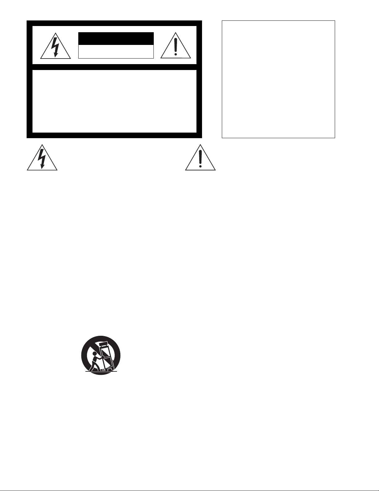
CAUTION
RISK OF ELECTRIC SHOCK
DO NOT OPEN
CAUTION:
TO PREVENT ELECTRIC SHOCK, MATCH
WIDE BLADE OF PLUG TO WIDE SLOT,
FULLY INSERT.
CAUTION: TO REDUCE THE RISK OF ELECTRIC SHOCK,
DO NOT REMOVE COVER (OR BACK).
NO USER-SERVICEABLE PARTS INSIDE.
REFER SERVICING TO QUALIFIED SERVICE PERSONNEL.
The lightening flash with arrowhead symbol,
within an equilateral triangle, is intended to
alert the user to the presence of uninsulated
“dangerous voltage” within the product's enclosure that may be of sufficient magnitude to
constitute a risk of electric shock to persons.
“WARNING”
“TO REDUCE THE RISK OF FIRE OR ELECTRIC SHOCK,
DO NOT EXPOSE THIS APPLIANCE TO RAIN OR MOISTURE.”
SAFETY INSTRUCTIONS
Read instructions - All the safety and operating instruc-
1.
tions should be read before the appliance is operated.
Retain instructions - The safety and operating instructions
2.
should be retained for future reference.
Heed warnings - All warnings on the appliance and in the
3.
operating instructions should be adhered to.
Follow instructions - All operating and use instructions
4.
should be followed.
Water and Moisture - The appliance should not be used
5.
near water - for example, near a bathtub, washbowl,
kitchen sink, laundry tub, in a wet basement, or near a
swimming pool, and the like.
Carts and Stands - The appliance should be used only
6.
with a cart or stand that is recommended by the manufacturer.
An appliance and cart combination should be moved with
care. Quick stops, excessive force, and uneven surfaces
may cause the appliance and cart combination to overturn.
Wall or Ceiling Mounting - The appliance should be
7.
mounted to a wall or ceiling only as recommended by the
manufacturer.
Ventilation - The appliance should be situated so that its
8.
location or position does not interfere with its proper ventilation. For example, the appliance should not be situated on a bed, sofa, rug, or similar surface that may block
the ventilation openings; or, placed in a built-in installation, such as a bookcase or cabinet that may impede the
flow of air through the ventilation openings.
ATTENTION:
POUR ÉVITER LES CHOCS ÉLECTRIQUES,
INTRODUIRE LA LAME LA PLUS LARGE DE
LA FICHE DANS LA BORNE CORRESPONDANTE DE LA PRISE ET POUSSER
JUSQU' AU FOND.
The exclamation point within an equilateral
triangle is intended to alert the user to the
presence of important operating and maintenance (servicing) instructions in the literature
accompanying the appliance.
Heat - The appliance should be situated away from heat
9.
sources such as radiators, heat registers, stoves, or other
appliances (including amplifiers) that produce heat.
Power Sources - The appliance should be connected to a
10.
power supply only of the type described in the operating
instructions or as marked on the appliance.
Grounding or Polarization - The precautions that should
11.
be taken so that the grounding or polarization means of
an appliance is not defeated.
Power Cord Protection - Power supply cords should be
12.
routed so that they are not likely to be walked on or
pinched by items placed upon or against them, paying
particular attention to cords at plugs, convenience receptacles, and the point where they exit from the appliance.
Cleaning - The appliance should be cleaned only as rec-
13.
ommended by the manufacturer.
Nonuse Periods - The power cord of the appliance should
14.
be unplugged from the outlet when left unused for a long
period of time.
Object and Liquid Entry - Care should be taken so that
15.
objects do not fall and liquids are not spilled into the enclosure through openings.
Damage requiring Service - The appliance should be ser-
16.
viced by qualified service personnel when:
The power supply cord or the plug has been damaged;
A.
or
Objects have fallen, or liquid has been spilled into the
B.
appliance; or
The appliance has been exposed to rain; or
C.
The appliance does not appear to operate normally or
D.
exhibits a marked changed in performance; or
The appliance has been dropped, or the enclosure
E.
damaged.
Servicing - The user should not attempt to service the ap-
17.
pliance beyond that described in the operating instructions. All other servicing should be referred to qualified
service personnel.
Page 3
This service manual is intended for qualified service technicians ; it is not meant for the casual doit-yourselfer. Qualified technicians have the necessary test equipment and tools, and have been
trained to properly and safely repair complex products such as those covered by this manual.
Improperly performed repairs can adversely affect the safety and reliability of the product and may
void the warranty. If you are not qualified to perform the repair of this product properly and safely,
you should not risk trying to do so and refer the repair to a qualified service technician.
WARNING
This product contains lead in solder and certain electrical parts contain chemicals which are known to the state of California to
cause cancer, birth defects or other reproductive harm.
Health & Safety Code Section 25249.6 Ð Proposition 65
NOTICE
(FOR CANADIAN MODEL ONLY)
Fuse symbols (fast operating fuse) and/or (slow operating fuse) on PCB indicate that replacement parts must
be of identical designation.
REMARQUE
(POUR MODÉLE CANADIEN SEULEMENT)
Les symboles de fusible (fusible de type rapide) et/ou (fusible de type lent) sur CCI indiquent que les pièces
de remplacement doivent avoir la même désignation.
CR300
(FOR USA MODEL ONLY)
SAFETY PRECAUTIONS
The following check should be performed for the continued
protection of the customer and service technician.
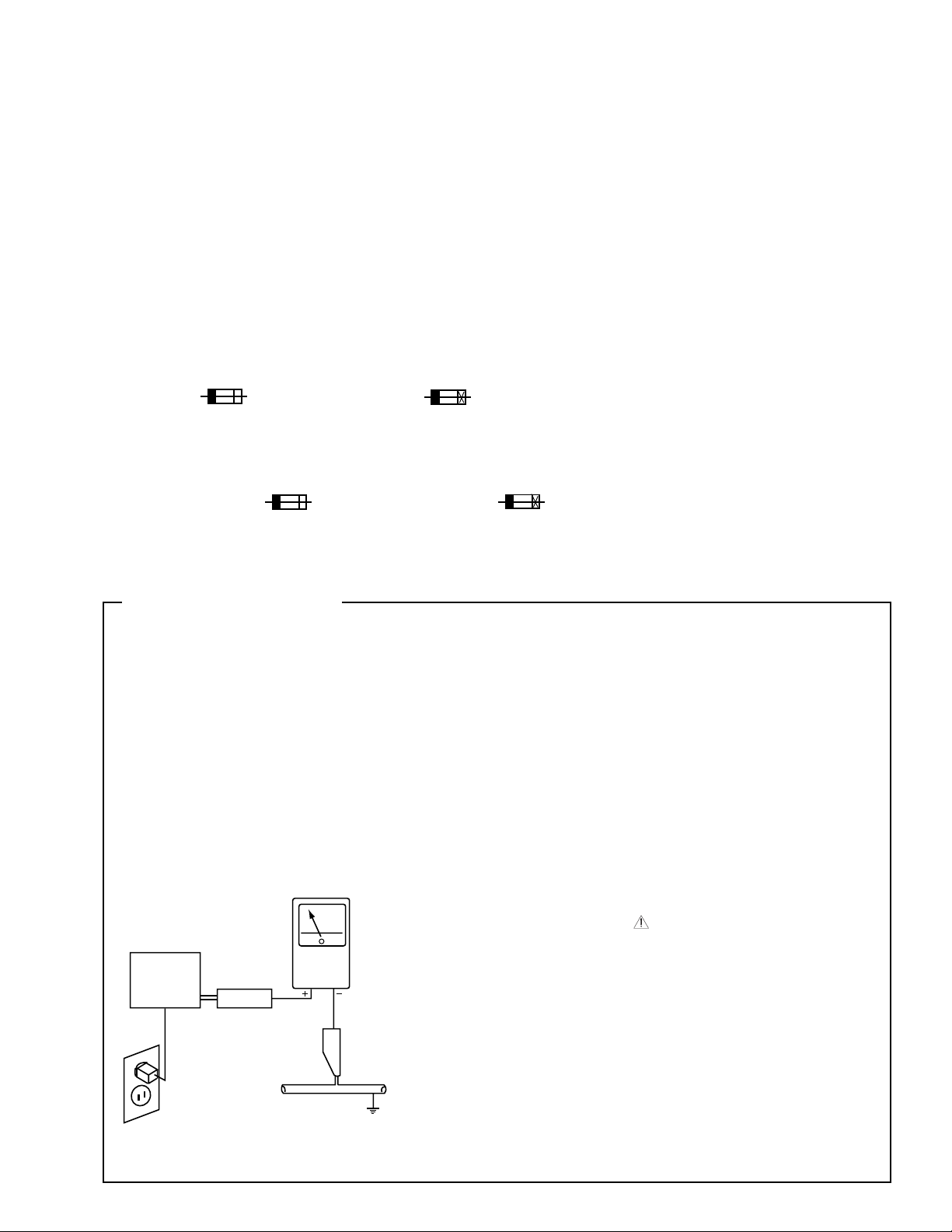
LEAKAGE CURRENT CHECK
Measure leakage current to a known earth ground (water
pipe, conduit, etc.) by connecting a leakage current tester
such as Simpson Model 229-2 or equivalent between the
earth ground and all exposed metal parts of the appliance
(input/output terminals, screw heads, metal overlays,
control shaft, etc.). Plug the AC line cord of the appliance
directly into a 120V AC 60Hz outlet and turn the AC power
switch on. Any current measured must not exceed 0.5mA.
Reading should
not be above
0.5mA
Device
under
test
Test all
exposed metal
surfaces
Leakage
current
tester
ANY MEASUREMENTS NOT WITHIN THE LIMITS
OUTLINED ABOVE ARE INDICATIVE OF A POTENTIAL
SHOCK HAZARD AND MUST BE CORRECTED BEFORE
RETURNING THE APPLIANCE TO THE CUSTOMER.
2. PRODUCT SAFETY NOTICE
Many electrical and mechanical parts in the appliance have
special safety related characteristics. These are often not
evident from visual inspection nor the protection afforded
by them necessarily can be obtained by using replacement
components rated for voltage, wattage, etc. Replacement
parts which have these special safety characteristics are
identified in this Service Manual.
Electrical components having such features are identified
by marking with a on the schematics and on the parts list
in this Service Manual.
The use of a substitute replacement component which does
not have the same safety characteristics as the PIONEER
recommended replacement one, shown in the parts list in
this Service Manual, may create shock, fire, or other
hazards.
Also test with
plug reversed
(Using AC adapter
plug as required)
AC Leakage Test
Earth
ground
Product Safety is continuously under review and new
instructions are issued from time to time. For the latest
information, always consult the current PIONEER Service
Manual. A subscription to, or additional copies of, PIONEER
Service Manual may be obtained at a nominal charge from
PIONEER.
3
Page 4
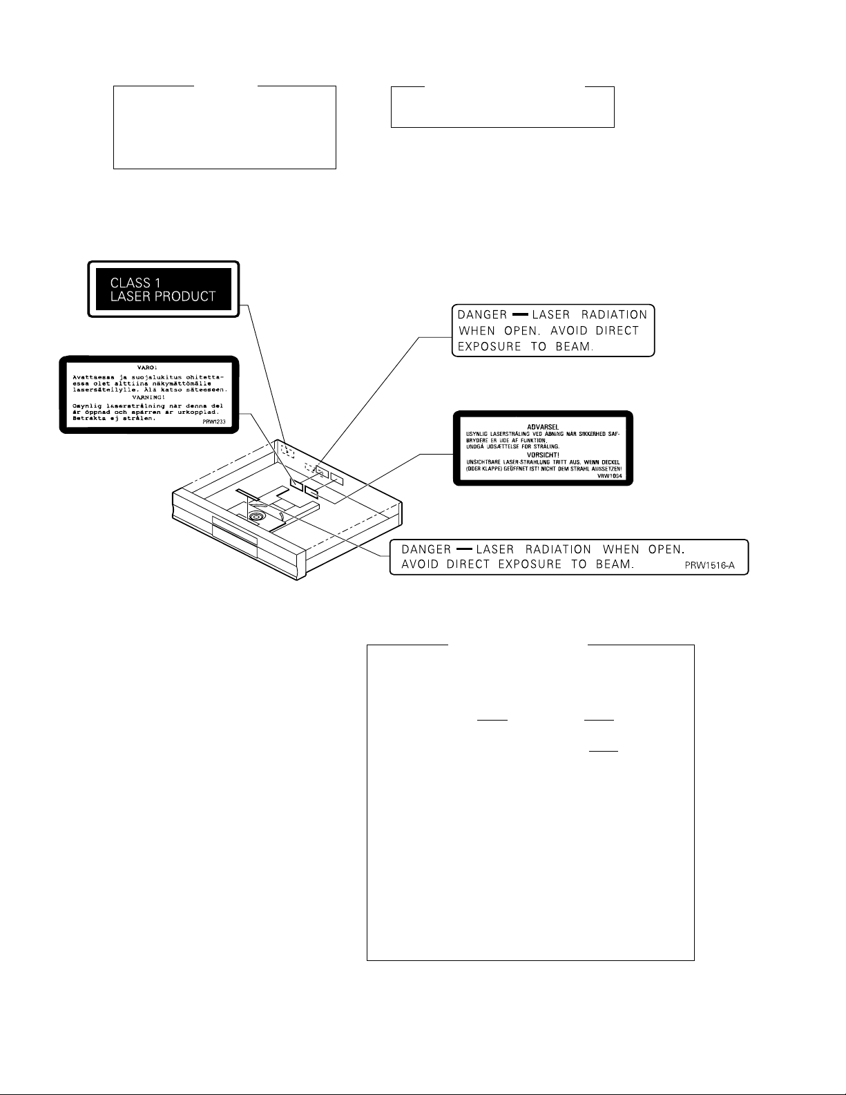
CR300
THIS PIONEER APPARATUS CONTAINS
LASER OF CLASS ΙΙΙ b.
SERVICING OPERATION OF THE APPARATUS
SHOULD BE DONE BY A SPECIALLY
INSTRUCTED PERSON.
LABEL CHECK
CR300 EUR
Printed on Rear Panel
CR300 EUR
IMPORTANT
LASER DIODE CHARACTERISTICS
MAXIMUM OUTPUT POWER: 23 mW
WAVELENGTH: 778 - 787 nm
CR300 USA
Printed on Rear Panel
CR300 EUR
Additional Laser Caution
1. Laser Interlock Mechanism
The position of the switch (S601) for detecting loading
state is detected by the system microprocessor, and the
design prevents laser diode oscillation when the switch
(S601) is not on CLMP terminal side (CLMP signal is OFF
or high level.). Thus, the interlock will no longer function if
the switch (S601) is deliberately set to CLMP terminal side
(low level).
The interlock also does not function in the test mode *.
Laser diode oscillation will continue, if pin 1 of M51593FP
(IC101) on the PRE-AMP BOARD ASSY mounted on the
pickup assembly is connected to GND, or pin 19 is
connected to low level (ON), or else the terminals of Q101
are shorted to each other (fault condition).
2. When the cover is opened with the servo mechanism block
removed and turned over, close viewing of the objective
lens with the naked eye will cause exposure to a Class 1
laser beam.
* Refer to page 13.
4
Page 5

TABLE OF CONTENTS
CR300
1. SPECIFICATIONS . . . . . . . . . . . . . . . . . . . . . . . . . . . . . . . . . .
2. CONTROLS, INDICATORS & CONNECTORS . . . . . . . . . . .
3. ADJUSTMENT PROCEDURES . . . . . . . . . . . . . . . . . . . . . . . . .
4. ASSEMBLING & DISASSEMBLING . . . . . . . . . . . . . . . . . .
5. EXPLODED VIEW, PCB ASSEMBLY & PARTS LIST . . . . .
6. CIRCUIT DIAGRAMS . . . . . . . . . . . . . . . . . . . . . . . . . . . . .
7. GENERAL INFORMATION . . . . . . . . . . . . . . . . . . . . . . . .
6
9
13
19
25
37
50
NOTES
Adjusting procedures, assembling & disassembling, exploded view, PCB assembly, parts list, circuit diagrams
*
and general information are given in this manual to assist the service technician in maintaining the Model
CR300.
CAUTION
Parts marked with this sign are safety critical components. They must always be replaced with identical
components. Refer to the Fostex Parts List and ensure exact replacement.
5
Page 6

CR300
1. SPECIFICATIONS
FUNCTION LIST
Automatic Disk Recognition
Sampling Rate Converter Automatic conversion (48 kHz, 32 kHz → 44.1 kHz)
Synchronous Recording Synchronous to one song / all songs / DAT ID
Auto Stop Delay in Digital Synchro 0 sec, 10 sec, off
Copy Bit Setting No restriction / one time only / prohibited
Auto Track Increment 6 levels
Manual Track Increment
REC MUTE
Fade In / Fade Out Fade time: 6 sec, 9 sec, 12 sec, 18 sec
PREVIOUS End section of previous track can be played back while in
Erase Mode (CD-RW) Last Track, All Track, Disc, TOC
Direct Search Operational through remote controller only
Track Search
Manual Search
One Song / All Song / Program Repeat Operational through remote controller only
Program Playback
Skip Playback
Sampling Monitor
Displayed Time Elapsed playback time, Remaining playback time,
Laser Hour Meter
Margin Display
Auto Pause
Auto Power Calibration
Remote Controller On / Off
Digital Out On / Off
Balanced Input Sensitivity Switching + 4 dBu / -10 dBV
ON/OFF switchable (44.1 kHz)
REC PAUSE mode
Total remaining playback time, Total playback time,
Elapsed recording time, Remaining recording time,
Total recording time
DISPLAY
FL Display Play, Pause, REC (Rec), RPT-1 (Repeat, 1-Repeat),
AUTO TRACK (Auto Track No.), PGM (Program),
FADER (Fader), SKIP ON (Skip ON/OFF),
32/44/48 (Input sampling frequency),
SYNC (Digital Synchronous Recording),
CD-RW/FINALIZE (Disc Type)
LED Display Track number, Level meter, Elapsed playback time,
Remaining playback time, Total remaining playback time,
Total playback time, Elapsed recording time,
Remaining recording time, Total recording time
INPUT/OUTPUT TERMINAL
Audio Input (Input Impedance) RCA pin (27 kΩ or more)
Balanced XLR-3 (10 kΩ)
Audio Output (Output Impedance) RCA pin (1 kΩ)
Balanced XLR-3 (1 kΩ or less)
6
Page 7
INPUT/OUTPUT TERMINAL (continued)
Digital Input (Input Impedance) Optical EIAJ CP-1201 TYPE2
Coaxial RCA IEC958 (75 Ω)
AES/EBU XLR-3 (110 Ω)
Digital Output (Output Impedance) Optical EIAJ CP-1201 TYPE2
Coaxial RCA IEC958 (75 Ω)
Headphone Output ∅ 6 (1/4 inch) standard stereo phone jack
Paralell Remote Control DIN 8-pin
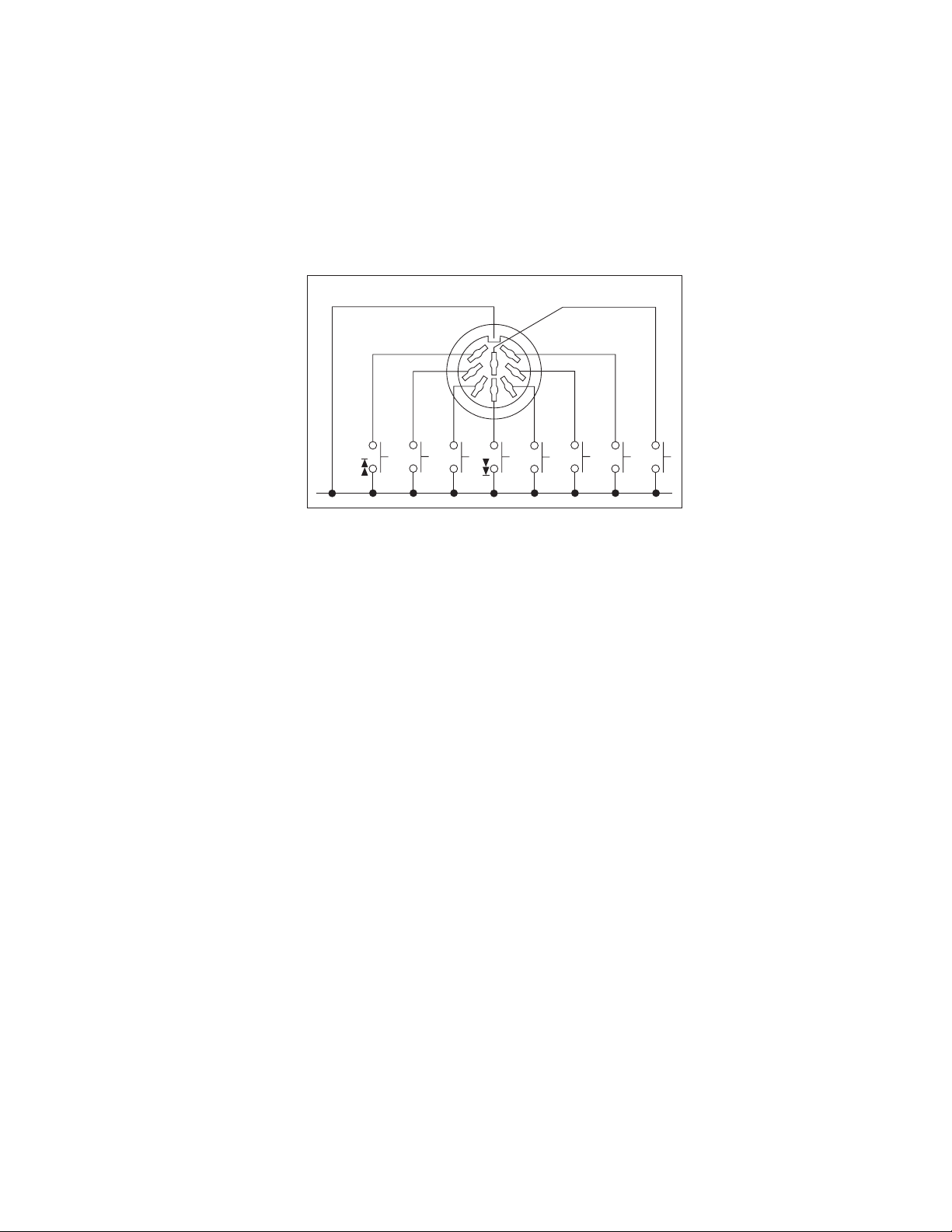
PARALLEL REMOTE TERMINAL
6
7
8
3
1
5
4
2
CR300
GND
PLAY
MANUAL TRACK
No. WRITE
PAUSE
REC
STOP
DIMENSIONS & WEIGHT
Maximum Dimensions 482 (W) x 105 (H) x 393 (D) mm
19 (W) x 4 - 1/8 (H) x 15 - 1/2 (D) inch
Weight (w/o package) 7.0 kg (15.4 lb)
POWER REQUIREMENT
Power Supply AC120 V, 60 Hz
AC220 ~ 230 V, 50/60 Hz
Power Consumption 24 W
AUDIO UNIT CHARACTERISTICS
CD Playback (Analog RCA Output)
Frequency Response 4 Hz ~ 20 kHz ± 1.0 dB (EIAJ)
S/N 100 dB or more (EIAJ)
Dynamic Range 90 dB or more (EIAJ)
Total Harmonic Distortion 0.01 % or less (EIAJ)
Channel Separation 90 dB or more (EIAJ)
De-emphasis Deviation 0 ± 1.5 dB or less (EIAJ)
Level Difference between Channels 1 dB or less (EIAJ)
Output Voltage 2.0 ± 0.3 Vrms (Load impedance: 10 kΩ, EIAJ)
Monitor (Analog RCA Input
→→
→ Analog RCA Output)
→→
Frequency Response 4 Hz ~ 20 kHz ± 1.0 dB (EIAJ)
S/N 83 dB or more (EIAJ)
Dynamic Range 83 dB or more (EIAJ)
Total Harmonic Distortion 0.01 % or less (EIAJ)
Maximum Input Level 3.2 Vrms or more (EIAJ)
Minimum Input Level 0.4 Vrms or less (EIAJ)
7
Page 8

CR300
AUDIO UNIT CHARACTERISTICS (continued)
Record & Playback (Analog RCA Input
→→
→ Analog RCA Output)
→→
Frequency Response 4 Hz ~ 20 kHz ± 1.0 dB (EIAJ)
S/N 83 dB or more
Dynamic Range 83 dB or more
Total Harmonic Distortion 0.01 % or less
Monitor (Digital Coaxial Input
→→
→ Analog RCA Output)
→→
Frequency Response 4 Hz ~ 20 kHz ± 1.0 dB (EIAJ)
S/N 95 dB or more (EIAJ)
Dynamic Range 90 dB or more (EIAJ)
Total Harmonic Distortion 0.01 % or less (EIAJ)
Maximum Input Level 0.6 Vp-p or more (EIAJ)
Minimum Input Level 0.2 Vp-p or less (EIAJ)
Record & Playback (Digital Coaxial Input
→→
→ Analog RCA Output)
→→
Frequency Response 4 Hz ~ 20 kHz ± 1.0 dB (EIAJ)
S/N 95 dB or more
Dynamic Range 90 dB or more
Total Harmonic Distortion 0.01 % or less
CD Playback (Analog XLR-3 +4 dBu Output)
Frequency Response 4 Hz ~ 20 kHz + 1.0, -1.5 dB (EIAJ)
S/N 100 dB or more (EIAJ)
Dynamic Range 90 dB or more (EIAJ)
Total Harmonic Distortion 0.01 % or less (EIAJ)
Channel Separation 90 dB or more (EIAJ)
De-emphasis Deviation 0 ± 1.5 dB or less (EIAJ)
Level Difference between Channels 1 dB or less (EIAJ)
Output Voltage 20 ± 1.5 dBm (Load impedance: 100 kΩ, EIAJ)
Output Voltage (-10 dBV) 8 ± 1.0 dBm (Load impedance: 100 kΩ, EIAJ)
Monitor (Analog XLR-3 +4 dBu Input
→→
→ Analog XLR-3 +4 dBu Output)
→→
Frequency Response 4 Hz ~ 20 kHz + 1.0, -1.5 dB (EIAJ)
S/N 83 dB or more (EIAJ)
Dynamic Range 83 dB or more (EIAJ)
Total Harmonic Distortion 0.01 % or less (EIAJ)
Maximum Input Level 13 Vrms or more (EIAJ)
Minimum Input Level (-10 dBV) 0.4 Vrms or less (EIAJ)
Record & Playback (Analog XLR-3 +4 dBu Input
→→
→ Analog XLR-3 +4 dBu Output)
→→
Frequency Response 4 Hz ~ 20 kHz + 1.0, -1.5 dB (EIAJ)
S/N 83 dB or more
Dynamic Range 83 dB or more
Total Harmonic Distortion 0.01 % or less
Specifications and appearance are subject to change without notice for product improvement.
8
Page 9
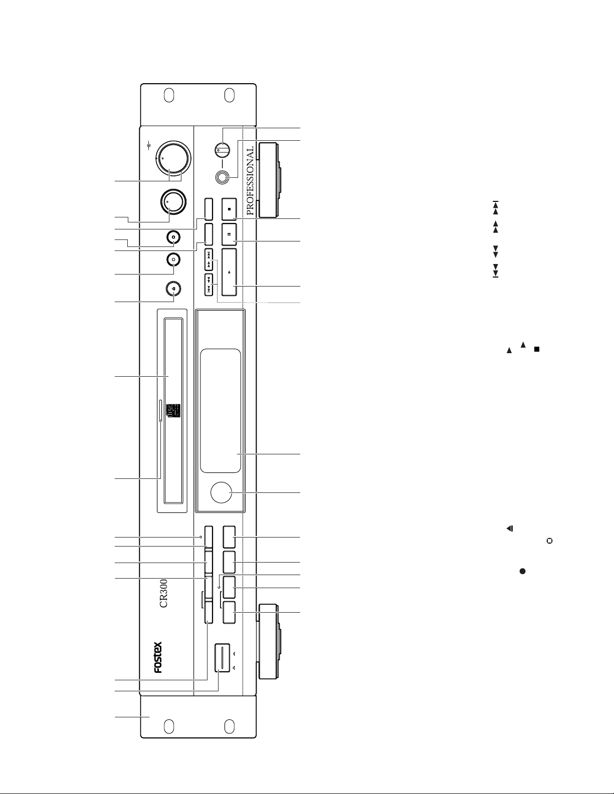
2. CONTROLS, INDICATORS & CONNECTORS
8
•
•
7
9
•
6
LR
5
••
4
•
•
ANALOG
•
XLR / +4
•
COAX XLR / -10
INPUT SELECTOR REC LEVELREC LEVEL
DIGITAL
REC
MUTE
RECORD
OPEN /
CLOSE
•
10
0
•
1
3
•
•
2
LINE
•
•
•
OPT
EBU
AES /
DIGITAL
TIME
LEVEL
PHONES
SYCHRO
/MARGIN
MAXMIN
]
DIGITAL SYNCHRO
[
]
]
]
REC LEVEL
]
TRACK NO. WRITE (MANUAL)
[
TRACK NO. AUTO/MANUAL
[
]
]
(outer: L ch, inner: R ch) [
FINALIZE
[
ERASE
[
CR300
]
[ ]
]
LEVEL MIN/MAX
[
PHONES
[
INPUT SELECTOR - DIGITAL (AES/EBU, OPT, COAX)
[
ANALOG (XLR/+4, XLR/-10, LINE)
14. Digital synchro button
15. Input selector
16. Record level knobs
17. Track number auto / manual button
18. Track number write (manual) button
19. Track number write (manual) indicator
20. Finalize button
21. Erase button
22. Remote control sensor
23. Display panel
24. Track / manual search buttons
25. Play button [ ]
26. Pause button [ ]
27. Stop button [ ]
28. Headphones jacks
29. Headphones level control
22 23 25 26 27 2924 28
]
7
MENUSET
FINALIZE ERASE
]
]
]
]
]
]
19
]
SKIP ID CLEAR
[
SKIP ID SET
[
POWER
[
]
SKIP PLAY
[
MENU
[
Recording : Light in read
Recording mute : Blinks in red
Playback : Lights in green
Erasing : Lights in orange
TIME/MARGIN
[
OPEN/CLOSE
[
REC MUTE
[
RECORD
[
COMPACT DISC RECORDER
WRITE
CLEAR SKIP PLAY
SKIP ID
(MANUAL)
TRACK NO.
AUTO /
MANUAL
OFF ON
POWER
17 18 20 21
1 2 3 4 5 6 8 10 11 1213 1614 159
< FRONT PANEL >
1. Rack mount angle
2. Power switch
3. SKIP ID set button
4. SKIP ID clear button
5. SKIP PLAY button
6. Menu button
7. Copy bit indicator
8. Function indicator
9. Disc tray
10. Open / close button
11. Record button
12. Time / margin button
13. Record mute button
9
Page 10
CR300
< DISPLAY PANEL >
Lights when automatic digitalsource synchro recording is
activated.
Lights during repeat
playback.
Lights in the program
mode.
Lights during random
playback.
Lights during record mode.
Blinks in the record muting
mode.
Lights when automatic track
number write during recording
is activated.
Lights during
playback.
Blinks during fade-in/out.
Lights or blinks
during pause.
Displays the track No.
Displays the elapsed playing time, remaining
playing time, total playing time, elapsed
recording time, remaining recording time,
total recording time and remaining time
until the end of finalization. (See below.)
Blinks during disc identification and
lights steadily.
CD: Lights when a disc is loaded.
CD-R: Lights if the loaded disc is a
CD-R disc before finalization.
CD-RW: Lights if the loaded disc is a
CD-RW disc
Lights if the loaded disc is a
finalized CD-RW disc.
Displays messages.
Displays the sampling
frequency (Fs) of the
current digital input.
All indicators are off
when the input signal
is interrupted.
Displays the input level during record
or the play level during playback
Lights, goes off or blinks during skip ID setting or
clearing.
The disc contains skip ID data, the SKIP ON indicator
lights automatically.
Switching the time display
The following operation allows you to check the recording time information during recording or playing time information
during playback. Every time the TIME button is pressed, the time information contents are switched in the order of A → B
→ C → D → A • • •.
The display mode varies depending on whether the current operation is recording or playing back (in the order of A → B →
C → A → • • • during recording).
During recording
A : Elapsed recording time
(2 min. 16 sec. after the
start of track No. 2)
C : Total recording time
(3 min. 50 sec. of 2track recording )
Remaining recording
B :
time (56 min. 10 sec.
remaining on the disc)
During playback
A : Elapsed playing time
(2 min. 16 sec. after the
start of track No. 1)
Total playing time
D :
(60 min. 0 sec. for 8
tracks)
B : Remaining playing time of track
being played (3 min. 20 sec.
remaining for track No.1)
Remaining playing time of all track
C :
on disc being played (46 min. 40
sec. remaining on the disc)
10
Page 11
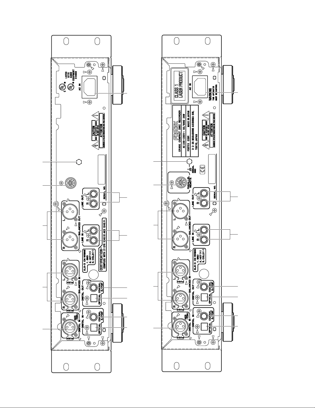
CR300
]
]
]
12
< REAR PANEL (USA version) >
11
10
< REAR PANEL (EUR version) >
12
]
S/P DIF COAXIAL DIGITAL IN
S/P DIF OPTICAL DIGITAL OUT
[
[
S/P DIF COAXIAL DIGITAL IN
[
]
]
LINE OUT
[
LINE IN
[
AC IN
[
7. Coaxial digital input
8. Optical digital output
9. Coaxial digital output
10. Line input
11. Line output
11
12. AC inlet
]
10
]
]
]
9
87
9
AES/EBU DIGITAL IN
[
BALANCED OUT
87
BALANCED IN
[
S/P DIF OPTICAL DIGITAL IN
[
output [
1 2 3 4 5
6
1 2 3 4 5
6
1. AES/EBU digital input
2. XLR balanced input
3. XLR balanced
4. Parallel remote connector
5. Earth terminal
6. Optical digital input
11
Page 12
CR300
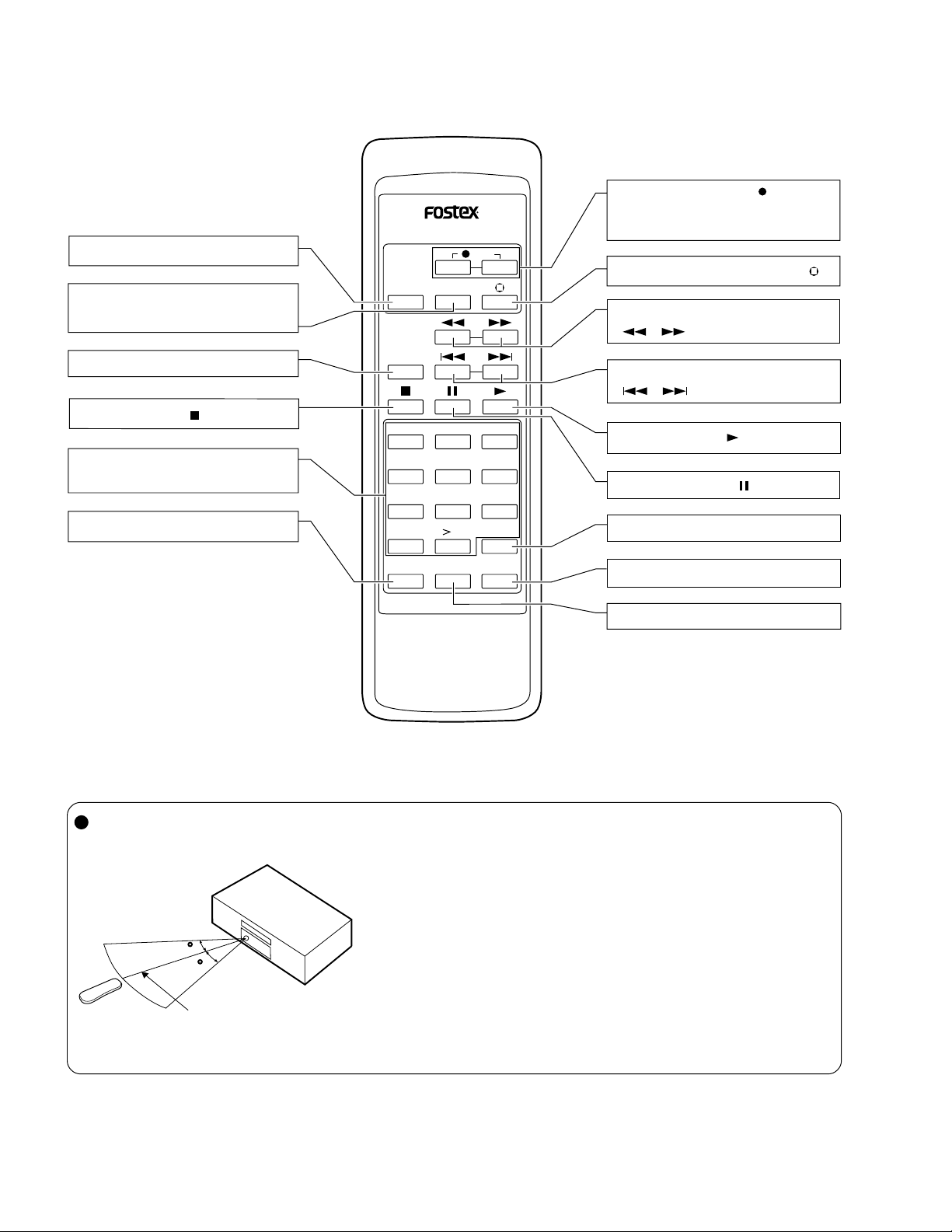
< REMOTE CONTROL UNIT MODEL 8317 >
FADER button
*TRACK No. WRITE
(MANUAL) button
REPEAT button
*Stop button ( )
Numeric buttons
(1 to 10, >10)
MODEL 8317
REC
TRACK NO.
FADER
REPEAT
WRITE
123
456
789
*Record buttons ( REC)
For recording, press the two
buttons simultaneously.
*Record muting button ( )
*Manual search buttons
,
( )
*Track search buttons
,
( )
*Play button ( )
*Pause button ( )
PGM (Program) button
Remote controllable range
30
30
7m(23 ft)
10
PGM CHECK CLEAR
10
TIME
*TIME button
CLEAR button
CHECK button
·
Remote control may be impossible if there is an obstacle between the
remote control unit and main unit or if the remote control unit is operated
at too great of an angle from the remote control sensor.
·
Erroneous operation may occur if strong light such as direct sunlight or
fluorescent lamp light is incident to the remote control sensor.
·
The main unit may operate erroneously if it is used near equipment
radiating infrared rays or if it is used near control unit of other equipment
is used near the unit. On the contrary, if this remote control unit is operated
near another piece of equipment which can be control wit infrared rays,
the equipment may operate erroneously.
·
Replace batteries when the remote controllable range decreases noticeably.
12
Page 13
3. ADJUSTMENT PROCEDURES
Short-circuit
Fig. 1 Enter the Test mode
SIDE B
FUNCTION ASSY
+ key
– key
Stop
Focus in
Fig.3 During adjustment of servo system (Input selector: optical)
FINALIZE button
Set
SET button
Average
DIGITAL
SYNCHRO
button
Mode switch
AUTO/MANUAL
button
(RECORD)
button
Sled move
buttons
(REC MUTE)
button
(STOP) button
Tracking close
(PAUSE) button
Spindle kick
(PLAY) button
,
TIME
/MARGIN
DIGITAL
SYCHRO
ANALOG
0
8
6
7
9
5
10
4
1
2
3
DIGITAL
REC
MUTE
OPEN /
CLOSE
RECORD
INPUT SELECTOR REC LEVELREC LEVEL
OPT
AES /
EBU
LINE
LR
COAX XLR / -10
XLR / +4
•
•
•
•
•
••••
•
•
•
•
•
•
•
PHONES
LEVEL
MAXMIN
MENUSET
POWER
OFF ON
COMPACT DISC RECORDER
CLEAR SKIP PLAY
FINALIZE ERASE
AUTO /
MANUAL
WRITE
(MANUAL)
SKIP ID
TRACK NO.
3-1. TEST DISCS
When adjusting the servo system, the following CD test discs should be used.
STD-903 or equivalent
STD-914 or equivalent
3-2. TEST EQUIPMENT
Laser Power Meter
(1)
The following power meter manufactured by Advantest Corporation, LEADER Corporation or equivalent:
TQ8210 + TQ82017 (Advantest Corporation)
TQ8215 + TQ82021 (Advantest Corporation)
TQ8215 + TQ82010 + TQ82017 (Advantest Corporation)
LE8010 (LEADER Corporation)
Audio Analyzer
(2)
Oscilloscope
(3)
Distortion Factor Meter
(4)
CD Jitter Meter
(5)
Block Error Rate Counter
(6)
CR300
3-3. TEST MODE
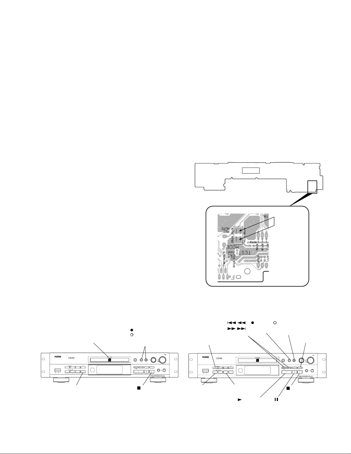
3-3-1. Test Mode
For adjustment, set the unit to the Test Mode. Referring to the Fig.
1 on the right, turn on the unit with the Test Mode short-circuit
pattern on the FUNCTION PCB Ass’y to enter the Test Mode. In
the Test Mode, all the displays (FL, LEDs) on the unit should be
lit. If not, turn the power off and repeat the same steps again.
3-3-2. Operation in Test Mode
In the Test Mode, the following adjustment functions are assigned
to the buttons, as explained in the Fig. 2 & 3.
LED for confirmation of
LD emission
COMPACT DISC RECORDER
SKIP ID
MENUSET
CLEAR SKIP PLAY
POWER
AUTO /
MANUAL
OFF ON
TRACK NO.
WRITE
FINALIZE ERASE
(MANUAL)
ERASE button
Switching CD, CD-R and CD-RW
Fig.2 During adjustment of LD power (Input selector: analog)
(RECORD) and
(REC MUTE)
buttons
LD emitting
REC
OPEN /
RECORD
MUTE
CLOSE
AES /
EBU
TIME
/MARGIN
(STOP) button
LD not emitting
INPUT SELECTOR REC LEVELREC LEVEL
ANALOG
DIGITAL
XLR / +4
•
COAX XLR / -10
•
•
OPT
LINE
•
•
•
DIGITAL
SYCHRO
PHONES
3
•
2
•
1
4
••••
•
0
LR
5
6
7
•
8
•
9
•
10
LEVEL
MAXMIN
13
Page 14
CR300
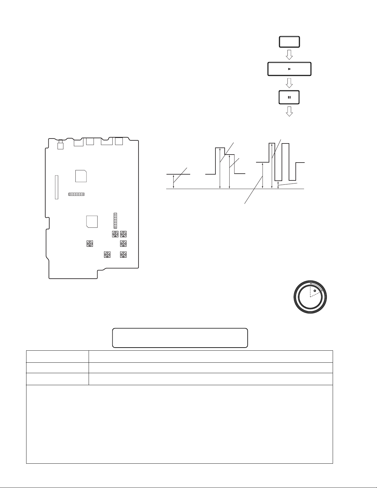
3-3-3. How to Playback a Disc in Test Mode
In the Test Mode, since each servo circuit operates independently, playing back a disc
requires that your operate the keys in the correct order to close the servo circuits.
Here is the key operation sequence for playing back a disc in the Test Mode.
Wait at least 2 ~ 3 seconds between each of these operations.
3-4. ADJUSTMENT 1 (LASER DIODE POWER ADJUSTMENT)
SERVO DIGITAL ASSY
CN354
1
6
CN102
1
6
VR102
R REC. PW1
VR101
PB. PW
VR106
RW REC.
PW2
VR103
R REC.PW2
VR104
RW REC.PW0
Fig. 4 Adjustment points
VR105
RW REC.
PW1
Playback power
Playback CD-R recording
Fig.5 Output power of the laser diode
Note 1: Attach the remote sensor of the laser power meter to a point angled away
about 10 degrees against the pickup lens and where the maximum power
is detected, so that there will be no light reflected onto the pickup.
Note 2: When adjusting with VR101 to VR106, first turn them completely counter-
clockwise and then adjust clockwise, so that the value to be reached is not
exceeded.
Note 3: Set the wavelength of laser power meter to 780 nm.
Note 4: The following adjustments 1 through 3 must be
done with the Input Selector set to the Analog position
(LD power adjustment mode).
CD-R overdrive
CD-RW erase
power
CD-R record
power
CD-RW recording
FINALIZE
CD-RW record power
CD-RW bias
power
INPUT SELECTOR
ANALOGDIGITAL
XLR / +4
•
COAX XLR / -10
•
•
AES /
EBU
OPT
•
•
LINE
•
3-4-1. Playback Power Adjustment
Pickup objective lens
VR101 (PB. PW)
0.60 mW ± 0.05 mW
14
Test Point
Adjustment Point
Adjustment Value
[Procedure]
Check that “CD” is displayed on the FL display. If “CD-R” or “CD-RW” is displayed, press the STOP button repeatedly
(1)
until “CD” is displayed.
Press the RECORD button. The LED for confirmation of LD emission will light in orange.
(2)
Press the REC MUTE button. The LED for confirmation of LD emission will light in red. The LD is emitting in this
(3)
status.
Turn VR101 clockwise until the adjustment value to be reached is obtained.
(4)
Press the STOP button to shut off the LD.
(5)
DANGER - LASER RADIATION WHEN OPEN.
AVOID DIRECT EXPOSURE TO BEAM.
Page 15

3-4-2. CD-R Record Power Adjustment
DANGER - LASER RADIATION WHEN OPEN.
AVOID DIRECT EXPOSURE TO BEAM.
CR300
Test Point
Adjustment Point
Adjustment Value
[Procedure]
Turn VR102 and VR103 fully counterclockwise to set their power output to minimum.
(1)
Press the ERASE button once so that “CD-R” appears on the FL display. If the indication is “CD” or “CD-RW”,
(2)
press the ERASE button repeatedly until “CD-R” is displayed on the FL display.
Press the RECORD button. The LED for confirmation of LD emission will light in orange.
(3)
Press the REC MUTE button. The LED for confirmation of LD emission will light in red. The LD is emitting in this
(4)
status.
CD-R record power adjustment
Turn VR102 clockwise until the adjusted value is 4.60 mW ± 0.1 mW.(5)
CD-RW overdrive power adjustment
Turn VR103 clockwise until the adjusted value becomes adjusted value at Step 5 above + (0.1 mW ± 0.01 mW).
(6)
Press the STOP button to shut off the LD.
(7)
Pickup objective lens
VR102 (R REC. PW1), VR103 (R REC. PW2)
VR102: 4.60 mW ± 0.1 mW
VR103: Addition of 0.1 mW ± 0.01 mW to the adjustment value of VR102
3-4-3. CD-RW Record Power Adjustment
DANGER - LASER RADIATION WHEN OPEN.
AVOID DIRECT EXPOSURE TO BEAM.
Test Point
Adjustment Point
Adjustment Value
[Procedure]
Turn VR104, VR105 and VR106 fully counterclockwise to set their power output to minimum.
(1)
Press the ERASE button twice so that “CD-RW” appears on the FL display. If the indication is “CD” or “CD-R”,
(2)
press the ERASE button repeatedly until “CD-RW” is displayed on the FL display.
Press the RECORD button. The LED for confirmation of LD emission will light in orange.
(3)
Press the REC MUTE button. The LED for confirmation of LD emission will light in red. The LD is emitting in this
(4)
status.
Turn the VR104 clockwise until the adjusted value is 0.40 mW ± 0.05 mW.
(5)
CD-RW record power adjustment
Turn VR106 clockwise until the adjusted value is 2.40 mW ± 0.1 mW.(6)
Pickup objective lens
VR104 (RW REC. PW0), VR106 (RW REC. PW2), VR105 (RW REC. PW1)
VR104: 0.40 mW ± 0.05 mW
VR106: 2.40 mW ± 0.1 mW
VR105: 5.90 mW ± 0.1 mW
CD-RW erase power adjustment
Turn VR105 clockwise until the adjusted value is 5.90 mW ± 0.1 mW.
(7)
Press the STOP button to shut off the LD.
(8)
15
Page 16
CR300
3-5. ADJUSTMENT 2 (SERVO SYSTEM ADJUSTMENT)
For servo adjustment, set the INPUT SELECTOR to OPTICAL.
INPUT SELECTOR
COAX XLR / -10
OPT
•
AES /
•
EBU
Use the RECORD and REC MUTE buttons to make the adjustments.
RECORD
To register an adjustment, press the (SKIP ID) SET button.
SET CLEAR
To reset the adjusted values to the initial settings, press and hold the
(SKIP ID) CLEAR button for 4 seconds.
•
XLR / +4
SKIP ID
ANALOGDIGITAL
•
•
LINE
•
REC
MUTE
SERVO DIGITAL ASSY
CN354 (TP201)
1
6
CN354
1 : RF
2 : TE
3 : TEIN
4 : VC
5 : FEIN
6 : FE
CN102
1
6
CN102
1 : VC
2 : TESTEQRFP
3 : TE
4 : MPP
5 : MPXOUT
6 : FMOUT
Fig. 6 Adjustment points
3-5-1. Focus Offset Adjustment
Test Point
Adjustment Point
Adjustment Value
[Procedure]
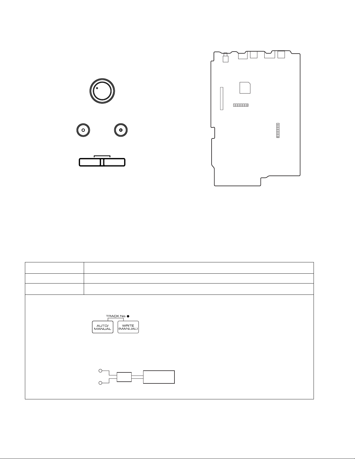
Press the AUTO/MANUAL button until “01_F4” appears on the FL display.(1)
Adjust with the RECORD and REC MUTE buttons until the value for Pin 6 of CN354 is 0 mV ± 10 mV.
(2)
Press the SET button to register the adjustment. Once the adjustment is registered with the SET button, “?” will
(3)
disappear.
CN354 - pin 6 (FE)
RECORD and REC MUTE buttons
0 mW ± 10 mW
16
FE
VC
10 : 1
10:1 probe
Oscilloscope
Page 17
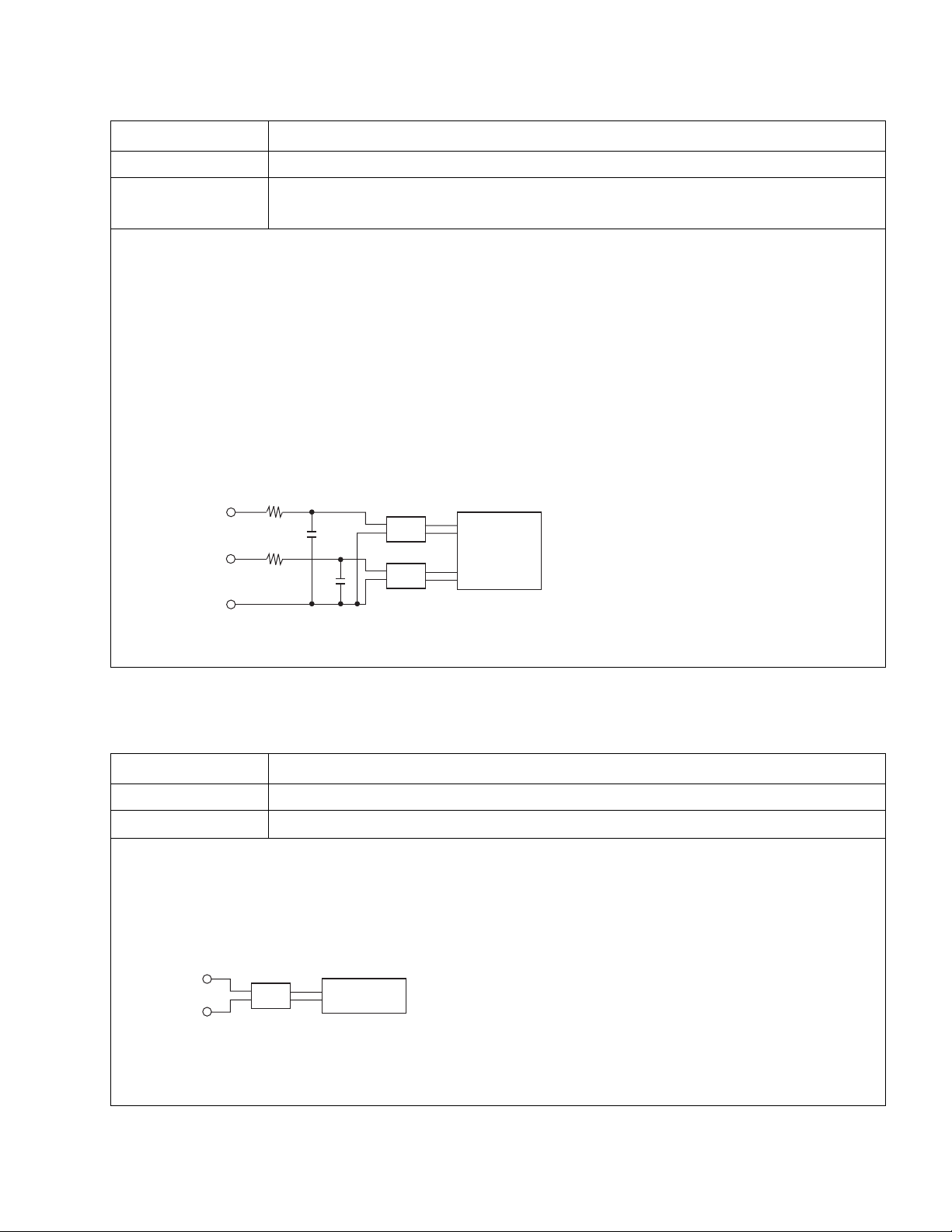
3-5-2. M-S Mix Ratio Adjustment
CR300
Test Point
Adjustment Point
Adjustment Value
CN102 - pin 3 (TE) and pin 4 (MPP)
RECORD and REC MUTE buttons
Adjust until the value of output signal from pin 3 (TE) and pin 4 (MPP) of CN102 are the same,
or the differential output of these signals is minimal.
[Procedure]
Press the AUTO/MANUAL button so that “02_F3” appears on the FL display.
(1)
Press the FINALIZE button for focus-in.
(2)
Press the PLAY button for CAV-servo spindle kick (the status where the spindle rotates with the focus servo on and
(3)
tracking servo off).
Adjust with the RECORD and REC MUTE buttons until the value to be reached is obtained.
(4)
Press the SET button to register the adjustment.
(5)
Once the adjustment is registered with the SET button, “?” on the FL display will disappear.
Press the STOP button to stop the unit.
(6)
NOTE: For adjustment, use the following circuits.
TE
MPP
VC
39kΩ
39kΩ
0.001µF
0.001µF
10 : 1
10 : 1
10:1 probe
CH1
CH2
Oscilloscope
NOTE: Adjustment must be done around mid-radius on a disc.
3-5-3. Tracking Offset Adjustment
Test Point
Adjustment Point
Adjustment Value
[Procedure]
Press the AUTO/MANUAL button so that “03_F6” appears on the FL display.
(1)
Press the RECORD and REC MUTE buttons until the above adjustment value to be reached is obtained.
(2)
Press the SET button to register the adjustment.
(3)
Once the adjustment is registered with the SET button, “?” on the FL display will disappear.
FE
VC
NOTE: Perform the adjustment in STOP mode.
This adjustment is possible with the low-pass filter used in adjustment 5 above attached.
CN354 - pin 2 (TE) or CN102 - pin 3 (TE)
RECORD and REC MUTE buttons
0 mV ± 10 mV
10 : 1
10:1 probe
Oscilloscope
17
Page 18

CR300
3-5-4. Focus Bias Adjustment
Test Point
Adjustment Point
Adjustment Value
CN354 - pin 1 (RF)
DIGITAL SYNCHRO, RECORD and REC MUTE buttons
Adjust until the RF jitter is minimal or that the eye pattern of the RF waveform is most open.
[Procedure]
Press the DIGITAL SYNCHRO button in Stop mode.
(1)
NOTE: Make sure that the unit is in Stop mode.
Check that “48” appears on the FL display.
(2)
Press the AUTO/MANUAL button so that “04_34” appears on the FL display.
(3)
Press the FINALIZE button for focus-in.
(4)
Press the PLAY button for CAV-servo spindle kick.
(5)
Press the PAUSE button to close the tracking servo, then set the unit to Playback mode.
(6)
Adjust with the RECORD and REC MUTE buttons until the above adjustment value to be reached is obtained.
(7)
Press the SET button to register the adjustment. Once the adjustment is registered with the SET button, “?” on the FL
display will disappear.
Press the STOP button to stop the unit.
(8)
RF
VC
10 : 1
10:1 probe
Jitter Meter
or
Oscilloscope
NOTE: Perform the adjustment in STOP mode.
This adjustment is possible with the low-pass filter used in adjustment 5 above attached.
18
Page 19
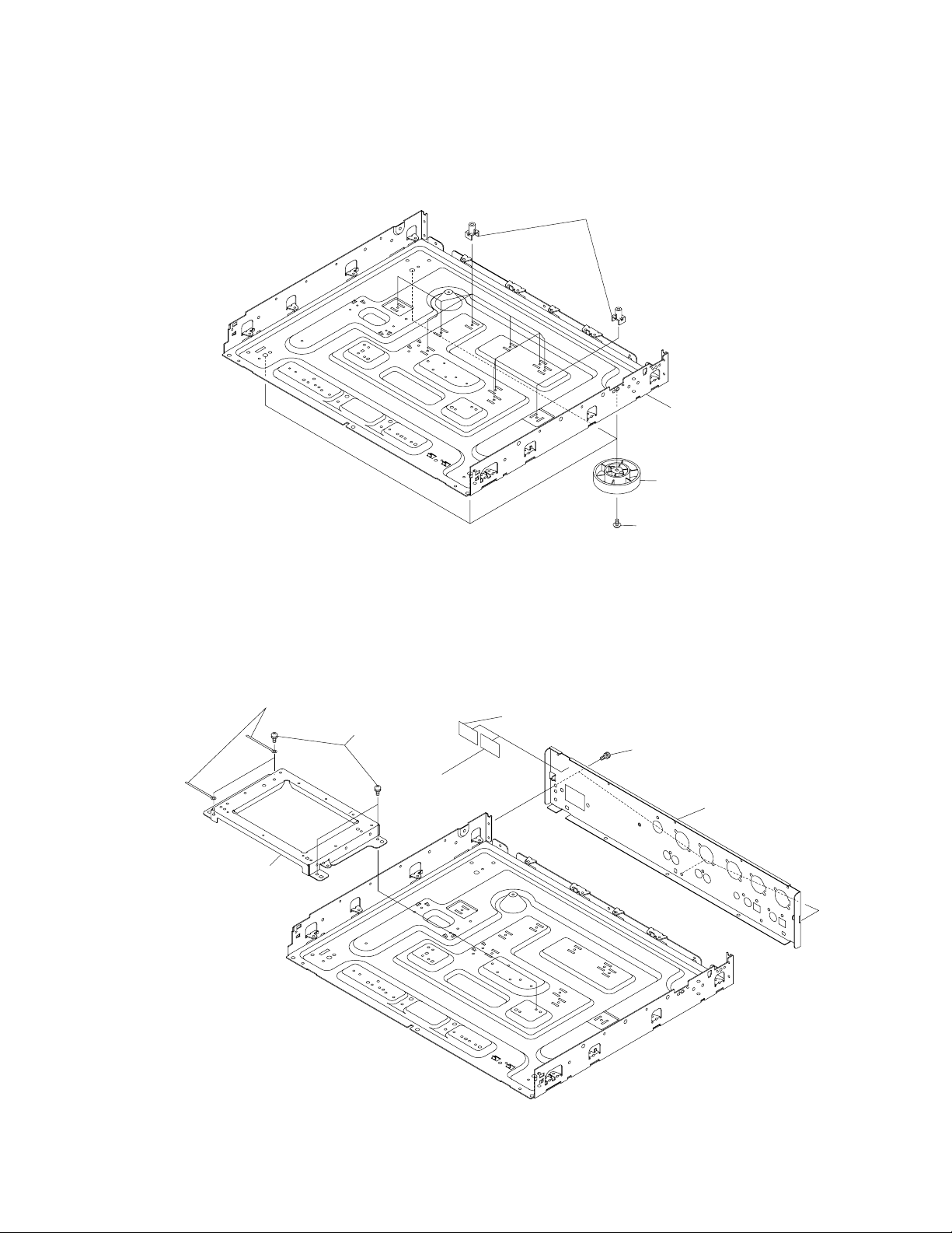
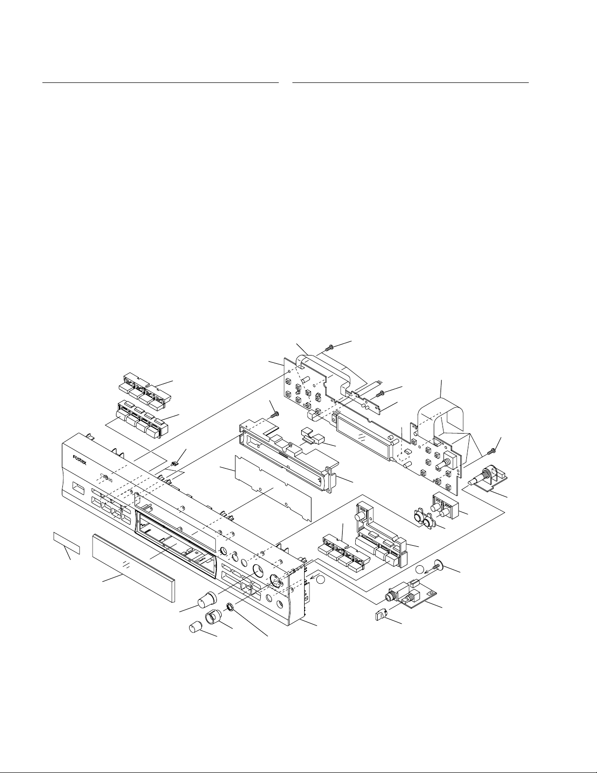
4. ASSEMBLING & DISASSEMBLING
Please refer to the following drawings for assembling & disassembling the CR300.
4-1. Under Base, PCB Mold & Insulator
PCB mold (N/A)
CR300
Under base (N/A)
Insulator, CR300
(8207013100)
4-2. Under Base, Mecha Base & Rear Base
Clamper, cord
(8221114000)
Screw, PBA1112
(8204188000)
Label, caution, EUR *
Mecha base
(N/A)
*: EUR version only
Label, caution, HE, CR300 *
(8218764000)
Screw, ABA1011
(8204178000)
(8218787000)
Screw, ABA1011
(8204178000)
Rear base
(EUR: 8221307006)
(USA: 8221307003)
19
Page 20

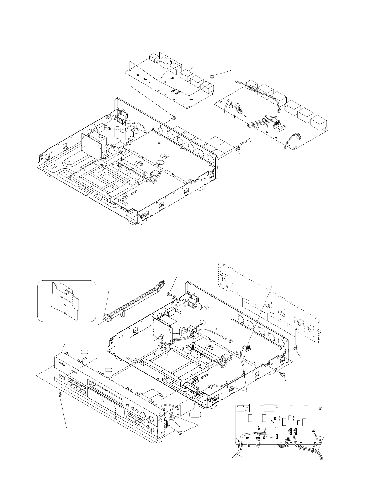
CR300
4-3. Transformer PCB Assy
Cord stopper
Transformer PCB assy
(8274241000)
Transformer cover
(N/A)
Rivet
(8207012700)
(N/A)
Screw, RBA1132
(8204179000)
Transformer, power
(EUR: 8242267006)
(USA: 8242267003)
4-4. Power, Audio & Servo Digital PCB Assys
Fuse, T500mA/250V, EUR
(8239119000)
Fuse, 1A/250V, USA
(8239118000)
Power PCB assy
(EUR: 8274236006)
(USA: 8274236003)
B12
Audio PCB assy
J2
(EUR: 8274235006)
(USA: 8274235003)
Screw, ABA1011
(8204178000)
Servo Digital PCB assy
(EUR: 8274232006)
(USA: 8274232003)
Terminal, screw, SI-A2475
(8245316000)
Screw,
BBZ30P080FCC
(8214379000)
20
Page 21

4-5. Power, Audio & Servo Digital PCB Assys Wiring
J2
IC308
Screw, ABA1011
(8204178000)
Screw, IBZ30P180FCC
(8204185000)
Screw, 3 x 6, B (8204158000)
Screw, ABA1011
(8204178000)
Screw, ABA1011
(8204178000)
Screw, 3 x 6, B
(8204158000)
Screw, IBZ30P180FCC
(8204185000)
Screw, IBZ30P180FCC
(8204185000)
Cord stopper
(N/A)
CR300
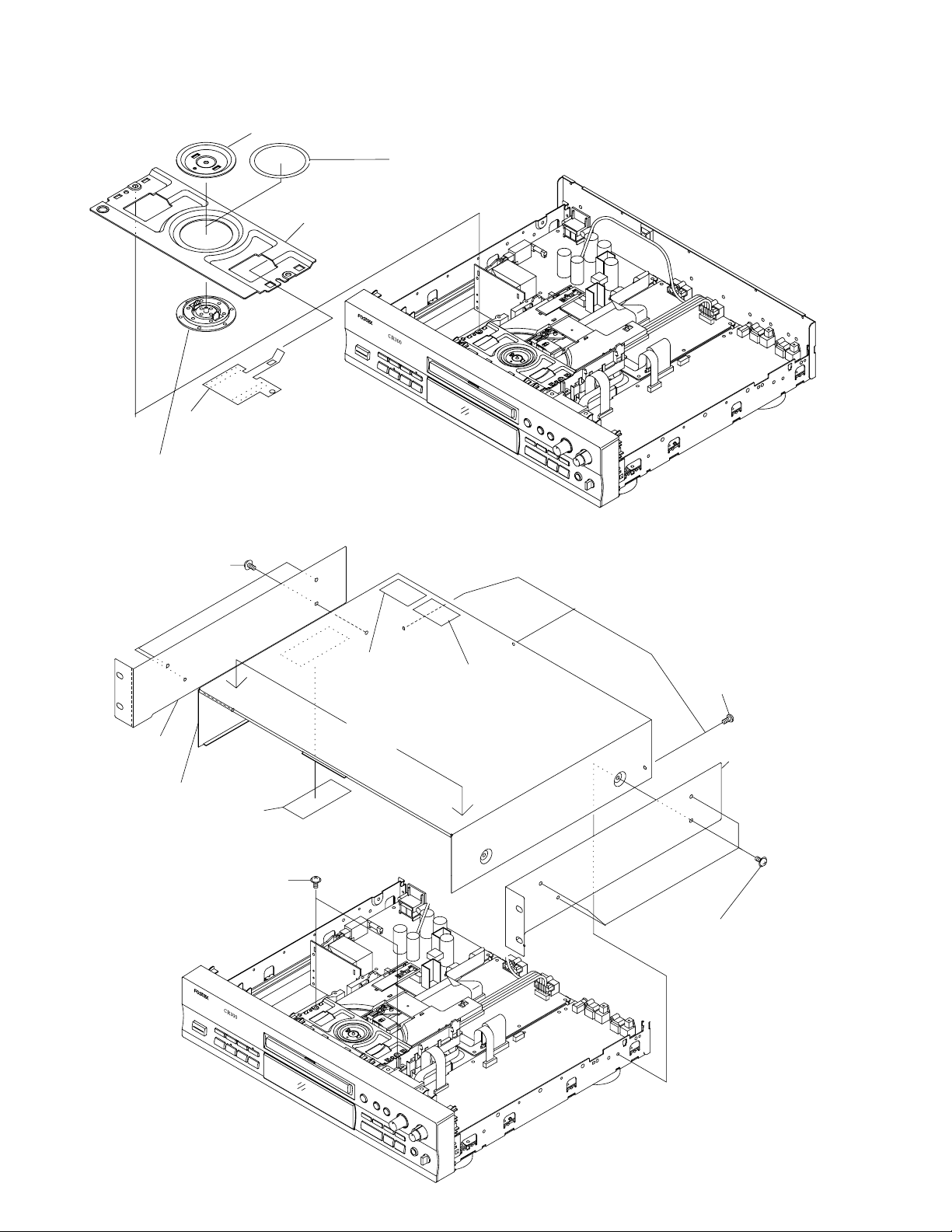
4-6. I/O Angle
Cable, 2mm pitch, parallel, 3P, L550
(8277480000)
Cord stopper
J4
(N/A)
B
4
0
1
B404
B
J801
4
0
2
FMEA
J21
Screw, IBZ30P200FMC (8204186000)
Screw, ABA1011 (8204178000)
I/O angle
(N/A)
Card spacer
(N/A)
C
N
8
0
3
CN302
Cable assy, 3P, wht
(8277484000)
Cable assy, 2mm pitch, 8P, red
(8277483000)
21
Page 22
CR300
4-7. Input PCB Assy
Input PCB assy
(EUR: 8274234006)
(USA: 8274234003)
Screw, ABA1011 (8204178000)
Screw, PMZ26P040FMC
(8204164000)
4-8. Input PCB Assy Wiring & Front Panel
K
N
8102
8021
C
C
N
8101
N
K
N
C
N
Screw, PMZ30P060FCC
(8204161000)
8
003
C
N
8
00
4
80
14
C
N
3002
Panel, front, CR300
(8212687000)
FMEA
FMEA
J709
C
O
M
P
A
C
T
D
I
S
C
R
E
C
O
R
D
E
R
Screw, IBZ30P080FZK
(8204184000)
Button, power, CR300
(8226251000)
Screw, 3 x 6, B
(8204158000)
J709
FMEA
J701
Screw, AMZ40P060FCU
(8204162000)
J11
J701
J3
02
2
N
C
CN805
CN403
FMEA
J851
Screw,
IBZ30P060FCC
(8214298000)
J709
Cable assy, 2mm pitch,
8P, wht
(8277482000)
8006
CN
8005
N
C
Screw,
IBZ30P080FZK
(8204184000)
Screw,
Binder
(N/A)
B12
IBZ30P060FCC
(8214298000)
CN8006
KN8017
KN8012
KN8010
22
J709
Page 23

4-9. Mechanism Assy Wiring
Screw,
IBZ30P100FCC
(8204180000)
CR300
Cable assy, 9P, grn
(8277486000)
A
Panel, tray, CR300
(8212688000)
Cable assy, 5P, grn
(8277485000)
C
O
M
P
A
C
T
D
I
S
C
R
E
C
O
R
D
E
R
4-10. Input, Power, Front PCB Assy Wiring
CN352
KN305
KN304
CN101
A
CN353
Cable, 2mm pitch,
parallel, 5P, L550
(8277497000)
J709
(To CN8006)
J701
(To CN51)
Cable, 2mm pitch,
parallel, 4P, L250
(8277487000)
Cable, 2mm pitch,
parallel, 3P, L350
(8277480000)
Cable, parallel, 9P, L150
(8277496000)
CN11
CN51
J11
CN401
To CN805
(VR PCB)
CN8006
CN8005
23
Page 24
CR300
4-11. Bridge, Clamper, etc.
Holder, tray, CR300
Clamper, CR300 (8212682000)
Plate, clamper, CR300(8221304000)
(8216720000)
Bridge, CR300
(8221305000)
C
O
M
P
A
C
T
D
I
S
C
R
E
C
O
R
D
Spacer, bridge, CR300(8212685000)
E
R
4-12. Bonnet & Angles
Screw, BBZ40P140FZK
(8204182000)
Angle, rack, FX,
L, CR300
(8221295000)
Bonnet, CR300 (8221306000)
Label, 65 ** (8218788000)
Screw, IPZ26P060FCU
(8214383000)
**: USA version only
Label, FCC,
CR300 **
(8221295000)
Label, DOC,
CR300 **
(8218790000)
Screw, IBP30P090FCC
(8204183000)
Angle, rack, FX,
R, CR300
(8221296000)
Screw, BBZ40P140FZK
(8204182000)
24
C
O
M
P
A
C
T
D
I
S
C
R
E
C
O
R
D
E
R
Page 25

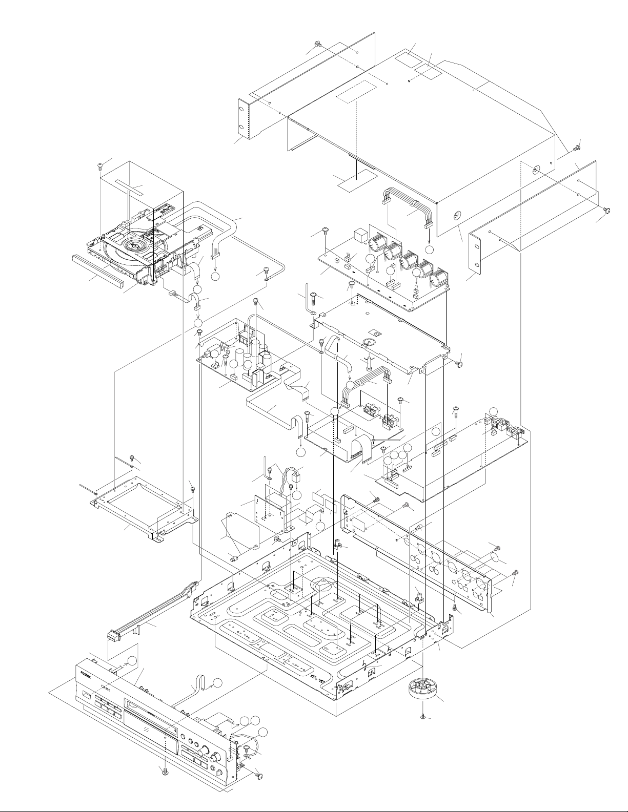
5. EXPLODED VIEWS, PCB ASSEMBLY & PARTS LIST
•
NOTE:
5-1. EXPLODED VIEWS
5-1-1. PACKING MATERIAL & ACCESSORY
Ref. No. Part No. Description
Parts marked by “N/A” are generally unavailable.
•
The mark found on some component parts indicate the importance of the safety factor of the parts. Therefore, when
replacing, be sure to use parts of identical designation.
•
Screws adjacent to mark on the product are used for disassembly.
Ref. No. Part No. Description
1 8276 9100 00 Cord, power, AC, USA
8276 9110 00 Cord, power, AC, EUR
2 8288 8901 00 Card, warranty, USA
3 8276 9120 00 Audio cable, RCA
4 8288 4370 00 Owner’s manual, ENG, CR300
5 N/A Caution, CD-R, EUR
N/A Caution, CD-R, USA
6 8270 8290 00 Remote control unit, Model 8317
7 N/A Cover, battery
8 N/A Battery, dry cell, manganese, UM-4
9 8228 4600 00 Protector, front, CR300
10 8228 4610 00 Protector, rear/top, CR300
11 8228 7300 00 Carton, inner, CR300
12 8228 9090 00 Carton, outer, CR300
13 8228 5750 00 Sheet, CR300
CR300
9 (2/2)
10 (1/3)
FRONT
10 (3/3)
9 (1/2)
10 (2/3)
13
11
12
6
8
7
5
2 (USA
version only)
4
3
1
25
Page 26

CR300
5-1-2. OVERALL EXPLODED VIEW
Ref. No. Part No. Description
1 8274 2320 06 PCB assy, Servo Digital, EUR, CR300
8274 2320 03 PCB assy, Servo Digital, USA, CR300
2 8274 2350 06 PCB assy, Audio, EUR, CR300
8274 2350 03 PCB assy, Audio, USA, CR300
3 8274 2360 06 PCB assy, Power, EUR, CR300
8274 2360 03 PCB assy, Power, USA, CR300
4 8274 2410 00 PCB assy, Transformer, CR300
5 8277 4800 00 Cable, 2mm pitch, parallel, 3P, L350
6 8277 4820 00 Cable assy, 2mm pitch, 8P, wht
7 8277 4850 00 Cable assy, 5P, grn
8 8277 4860 00 Cable assy, 9P, grn
9 8242 2670 06 Transformer, power, EUR, CR300
8242 2670 03 Transformer, power, USA, CR300
10 8239 1190 00 Fuse, T500mA/250V, EUR
8239 1180 00 Fuse, 1A/125V, USA
11 8204 1780 00 Screw, ABA1011
12 8204 1580 00 Screw, 3 x 6, B
13 N/A PCB mold
14 N/A Cord stopper
15 8221 3060 00 Bonnet, CR300
16 N/A Under base
17 8221 3070 06 Base, rear, EUR, CR300
8221 3070 03 Base, rear, USA, CR300
18 N/A Mecha base
19 . . .
20 . . .
21 8207 0131 00 Insulator, CR300
22 . . .
23 8221 1140 00 Clamper, cord
24 8204 1880 00 Screw, PBA1112
25 . . .
26 . . .
27 8226 2510 00 Button, power, FX, CR300
28 8212 6880 00 Panel, tray, CR300
29 8214 3790 00 Screw, BBZ30P080FCC
30 8214 2980 00 Screw, IBZ30P060FCC
31 8204 1800 00 Screw, BBZ30P100FCC
32 . . .
33 . . .
34 8204 1850 00 Screw, IBZ30P180FCC
35 . . .
36 8218 7680 00 Label, black
37 8218 7870 00 Label, caution, HE, CR300
38 8218 7640 00 Label, caution, EUR
39 8218 7880 00 Label, 65, CR300
40 N/A Laser caution label
41 8245 3160 00 Terminal, screw, SI-A2475
42 8204 1790 00 Screw, RBA1132
Ref. No. Part No. Description
43 N/A Transformer cover
44 8207 0127 00 Rivet
45 8204 1810 00 Screw, BBZ40P080FCC
46 8216 7210 00 Cover, fuse, CR300
47 8277 4830 00 Cable assy, 2mm pitch, 8P, red
48 N/A I/O angle
49 N/A Card spacer
50 8204 1860 00 Screw, IBZ30P200FMC
51 8204 1610 00 Screw, PMZ30P060FCC
52 8204 1640 00 Screw, PMZ26P040FMC
53 8204 1840 00 Screw, IBZ30P080FZK
54 N/A Binder
55 8204 1620 00 Screw, AMZ40P060FCU
56 8221 2950 00 Angle, rack, FX, L, CR300
57 8221 2960 00 Angle, rack, FX, R, CR300
58 8204 1820 00 Screw, BBZ40P140FZK
59 8218 7890 00 Label, FCC, CR300
60 8218 7900 00 Label, DOC, CR300
61 8204 1830 00 Screw, IBP30P090FCC
62 8274 2340 06 PCB assy, Input, EUR, CR300
8274 2340 03 PCB assy, Input, USA, CR300
63 8277 4840 00 Cable assy, 3P, wht
64 8277 4870 00 Cable, 2mm pitch, parallel, 4P, L250
65 8277 4890 00 Cable, 2mm pitch, parallel, 6P, L300
66 8277 4900 00 Cable, 2mm pitch, parallel, 8P, L200
67 8277 4910 00 Cable, 2mm pitch, parallel, 15P, L100
68 8277 4920 00 Cable assy, 2P
69 8277 4930 00 Cable assy, 2mm pitch, 6P
70 8277 4940 00 Cable, 32P, FCC/30V
71 8277 4960 00 Cable, parallel, 9P, L150
72 8277 4970 00 Cable, 2mm pitch, parallel, 5P, L550
26
Page 27
CR300
59**
58
56
31
39**
40**
60**
61
12
28
Refer to “4.4 LOADING
MECHANISM ASSY.”
24
23
18
8
11
70
I
C
7
12
62
14
50
69
L
11
6
G
K
M
15
58
57
12
B
11
46
10
D
E
J
34
3
65
42
24
14
4
43
44
55
12
A
52
30
34
M
63
51
5
49
66
34
H
47
48
K
11
14
11
A
2
68
37*
D
9
1
67
11
38*
J
71
C
B
I
F
45
41
13
36
13
53
27
72
C
O
M
P
A
C
T
D
I
S
C
R
E
C
O
R
D
E
R
Refer to “4-1-3. FRONT
L
PANEL SECTION.”
54
64
E
16
29
17
21
11
53
H
F
G
*: EUR version only
**: USA version only
30
30
27
Page 28
CR300
5-1-3. FRONT PANEL SECTION
Ref. No. Part No. Description
1 8274 2380 00 PCB assy, Function A, CR300
2 8274 2390 00 PCB assy, HP, CR300
3 8274 2400 00 PCB assy, VR, CR300
4 8277 4810 00 Cable, 22P F.F.C/60V
5 8204 1770 00 Screw with washer, ABA1005
6 8226 2540 00 Knob, headphone, FX, CR300
7 8226 2550 00 Button, mode, FX, CR300
8 8226 2560 00 Button, manual, FX, L, CR300
9 8226 2580 00 Button, REC, FX, CR300
10 . . .
11 8226 2570 00 Button, manual, FX, R, CR300
12 8226 2610 00 Knob assy, VOL, CR300
13 8226 2520 00 Knob, REC, FX, L, CR300
14 8226 2530 00 Knob, REC, FX, R, CR300
15 8216 7180 00 Sheet, FL, CR300
Ref. No. Part No. Description
16 8212 6660 00 Window, FL, CR300
17 8212 6670 00 Lens, LED, CR300
18 8226 2600 00 Ring, REC, CR300
19 8212 6680 00 Lens, operation, CR300
20 8212 6860 00 Panel, sub, CR300
21 8212 6870 00 Panel, front, CR300
22 8226 2590 00 Button, play, FX, CR300
23 8204 1870 00 Screw, PPZ30P100FMC
24 . . .
25 N/A Getter label, USA
26 8236 0841 00 IC, EPROM, CR300
27 8277 4880 00 Cable, 2mm pitch, parallel, 5P, L150
28 8274 2420 00 PCB assy, Function B, CR300
25
27
23
1
8
23
23
28
4
7
26
23
17
C
O
M
P
A
C
T
D
IS
C
R
E
C
O
R
D
E
R
15
19
20
3
11
9
18
22
16
12
14
13
Accessories for the VR ASSY
A
A
21
6
5
2
28
Page 29

5-1-4. LOADING MECHANISM SECTION
· Bottom View
8
17
11
3
21
28
9
23
22
24
5
2
18
20
12
Loading Base
13
6
4
26
26
29
25
19
15
1
14
16
10
7
27
A
A
30
31
Ref. No. Part No. Description
1 8277 4940 00 Cable, 32P, FCC/30V
2 N/A Earth lead unit
3 8277 4950 00 Cable assy, 2P, CR300
4 8249 0430 00 DC motor, CR300
5 8204 1900 00 Screw, DBA1055
6 N/A Motor pulley
7 8204 1910 00 Screw, VBA1055
8 8214 3920 00 Spring, tray stopper, CR300
9 8216 7190 00 Belt, rubber, CR300
10 8212 6760 00 Base, loading, CR300
11 8212 6770 00 Tray, CR300
12 8212 6780 00 Pulley, gear, CR300
13 8212 6790 00 Gear, loading, CR300
14 8212 6800 00 Gear, drive, CR300
15 8212 6810 00 Cam, drive, CR300
CR300
Ref. No. Part No. Description
16 8212 6830 00 Plate, lock, CR300
17 8212 6840 00 Stopper, tray, CR300
18 N/A CD-RW servo mecha assy
19 8204 1510 00 Screw, BBZ26P040FMC
20 8214 3840 00 Screw, IPZ20P080FMC
21 8260 5710 00 Loading motor assy, CR300
22 N/A Loading mechanism assy
23 8221 3040 00 Plate, clamper, CR300
24 8221 3050 00 Bridge, CR300
25 8212 6820 00 Clamper, CR300
26 8214 3830 00 Screw, IPZ26P060FCU
27 N/A Loading A assy
28 N/A Loading B assy
29 8216 7200 00 Holder, tray, CR300
30 8212 6850 00 Spacer, bridge, CR300
31 8221 3080 00 Stopper, CR300
29
Page 30

CR300
5-1-5. SERVO MECHANISM SECTION
Ref. No. Part No. Description
1 N/A PCB assy, Servo Mech
2 8260 5670 00 DC motor assy, CR300
3 N/A DC motor
4 8216 7160 00 Rubber, float, A, CR300
5 8216 7170 00 Rubber, float, B, CR300
6 N/A Rack spring
7 N/A Mirror sheet
8 8212 6690 00 Base, servo, CR300
9 8212 6700 00 Gear, pinion, CR300
10 8212 6710 00 Gear, A, CR300
11 8212 6720 00 Gear, B, CR300
12 8212 6730 00 Gear, C, CR300
13 8212 6740 00 Rack, CR300
Ref. No. Part No. Description
14 8212 6750 00 Stopper, rack, CR300
15 N/A Disc table
16 8221 3030 00 Base, carriage, S, CR300
17 . . .
18 8223 3000 00 Bar, guide, CR300
19 8223 3010 00 Bar, guide, sub, CR300
20 N/A Magnet
21 8260 5680 00 Pickup, CD-R, CR300
22 8204 1930 00 Screw, IPZ20P060FMC
23 8204 1940 00 Screw, PMZ20P030FMC
24 8204 1890 00 Screw, JGZ17P030FMC
25 8260 5690 00 Disc table assy, CR300
26 8260 5700 00 Carriage motor assy, CR300
22
25
15
20
10
9
7
23
2
3
26
11
16
19
18
· Bottom View
SERVO MECH ASSY
14
6
13
Carriage Base S
24
22
12
How to Install the Disc Table
1
1
4
21
5
Use nippers or other tool to cut the two sections marked A in figure
2
While supporting the spindle motor shaft with the stopper, put spacer on
top of the carriage base, and stick the disc table on top (takes about 9kg
pressure). Take off the spacer.
Spacer
A
2
Spacer setting
Position
(Pressure of about 9kg)
Disc table Assy
1
A
1
.
30
8
Spacer
Servo Base
Spacer
Spindle
motor
OK NG
Stopper
11mm
2.8mm
Carriage
Base
PCB
Page 31

CN51
POWER PCB
CN8006
INPUT PCB
INPUT PCB
CN8005
ASS'Y
VR PCB
CR300
FUNCTION B PCB ASS'Y
FUNCTION A PCB ASS'Y
CN11
POWER PCB
SERVO DIGITAL PCB
CN202
PCB ASS'Y
HEADPHONE
CN401
AUDIO PCB
CN1
POWER PCB
TRANSFORMER PCB ASS'Y
Parts Side
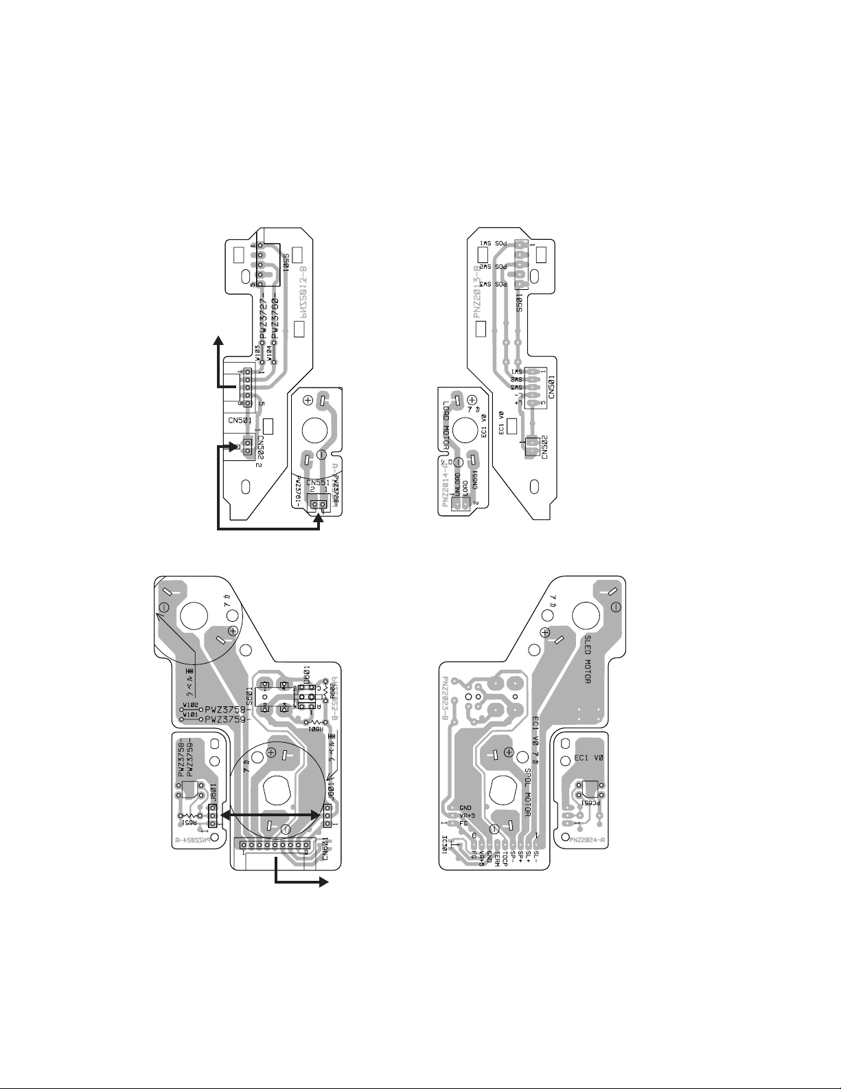
5-2. PCB ASSEMBLIES
5-2-1. FUNCTION, TRANSFORMER, VR & HEADPHONE PCBs
Foil Side
31
Page 32

CR300
CN3002
INPUT PCB
J801
AUDIO PCB
J21
POWER PCB
CN601
PICKUP ASS'Y
SERVO DIGITAL PCB ASS'Y
32
CN501
LOADING A PCB
CN601
MECHA PCB
5-2-2. SERVO DIGITAL PCBs
Parts side
PCB
CN601
FUNCTION A
Page 33

CR300
Foil side
33
Page 34

CR300
SERVO
DIGITAL
PCB
CN302
INPUT PCB ASS'Y
VR PCB
CN805
AUDIO PCB
CN803
FUNCTION
A PCB
J709
AUDIO PCB
J408
AUDIO PCB
J407B
AUDIO PCB
J408
INPUT PCB
CN8101
CN403
H.P. PCB
AUDIO PCB ASS'Y
CN8004
INPUT PCB
SERVO
DIGITAL
PCB
CN355
TRANS-
FORMER
PCB
CN355
POWER PCB ASS'Y
CN355
FUNCTION A PCB
CN355
TRANSFORMER PCB
34
CN8101
CN8102
INPUT PCB
INPUT PCB
5-2-3. AUDIO, INPUT & POWER PCBs
Parts side
Page 35

CR300
Foil side
35
Page 36
CR300
5-2-4. LOADING A / B & SERVO MECH PCBs
LOADING A PCB ASS'Y
SERVO
DIGITAL PCB
CN352
LOADING B
PCB ASS'Y
SERVO MECH
PCB ASS'Y
SERVO DIGITAL PCB
CN353
36
Page 37

8274239000
HP PCB ASS'Y
Rch
GNDA
Lch
CN403CN401
123
3
2
1
PIN RIN
RGND
VRROUT
RGND
LGND
VRLOUT
1234567
V+5
GND
DIN
LGND
PIN LIN
8
CN3002
CN8004
Lch
GND
CN8102
1
2
Rch
CN8101
123
GND
AMUTE
GND
4
USA: 8274234003
EUR: 8274234006
INPUT PCB ASS'Y
V+12
GND
V-12
CN8003
123
CN8005
VRLIN
8
GNDA
7
VRLOUT
6
GNDA
5
GNDA
4
VRROUT
3
GNDA
2
VRRIN
1
REMOTE
5
IN GAIN
4
IN SEL
3
OUT GAIN
2
GND
1
CN8006
CR300
CN805
VRLIN
8
GNDA
7
VRLOUT
6
GNDA
5
GNDA
4
VRROUT
3
GNDA
2
1
VRRIN
8274240000
VR PCB ASS'Y
123
Lch
Rch
GNDA
USA: 8274235003
EUR: 8274235006
AUDIO PCB ASS'Y
ADLRCK
ADBCK
ADDATA
ADSTBY
AMUTE
J801
CN301
V+5
3
GND
2
DIN
1
CN302
LRSTDICL
123456789101112131415
123456789
LRST
ADBCK
AMUTE
ADSTBY
ADLRCK
ADDATA
1234567
CN803
RGND
PIN RIN
VRROUT
DEEM
DACBCK
1011121314
DI
CL
DEEM
DACBCK
LGND
RGND
VRLOUT
DACDATA
DACLRCK
GNDD
GNDD
DACDATA
DACLRCK
8
Lch
LGND
PIN LIN
Rch
J408
AMUTE
J407B
V-12A
8
GNDA
7
V+12A
6
GNDA
5
V+5A
4
V-AU
3
GNDU
2
V+AU
1
CN402
MCK
GNDD
15
MCK
GNDD
EUR: 8274232006
USA: 8274232003
SERVO DIGITAL PCB ASS'Y
8
7
6
5
4
3
2
1
J21
CN355
V-12A
GNDA
V+12A
GNDA
V+5A
V-AU
GNDU
V+AU
J31
V+5A
GNDA
V+5D
12345
12345
V+5A
V+5D
GNDA
J32
GNDD
GNDD
123
V+12
V+U
V+U
V-12
GND
INLET
CN1
NEUTRAL
2
LIVE
1
CN2
SEB
9
SEA
8
AUB
7
GND
6
AUA
5
AC2
4
AC1
-27V
AC2
AC1
4
GND
FL
CN51
3
2
1
CN11
USA: 8274236003
EUR: 8274236006
POWER PCB ASS'Y
GNDU
GNDS
6
123
6
GNDU
CN202
9604S-22C
J1
2
1
SEB
9
SEA
8
AUB
7
6
AUA
5
AC2
4
AC1
3
2
FL
1
J11
FSC/XTHR
22
XVCO
21
EECS
20
REMCON
19
MREQ
18
XPFAIL
17
UNLOCK
16
LREQ
15
MACK
14
XOPT
13
XRST
12
XFUSE
11
MSO
10
MSCK
9
MSI
8
DEEM
7
GNDD
6
GNDD
5
GNDD
4
GNDD
3
V+5D
2
V+5D
1
POWER CORD
NEUTRAL
LIVE
8242267003
Transformer
USA
GND
GND
TRANSFORMER PCB ASS'Y
1.25mm PITCH FFC
8242267006
EUR
8274241000
4
3
2
1
1
2
3
4
5
6
7
8
9
10
11
12
13
14
15
16
17
18
19
20
21
22
PITCH WIDTH
2mm PITCH PARALLEL CABLE 2mm PITCH CN ASS'Y 2.5mm PITCH PARALLEL CABLE
12345
J709
GND
IN GA
IN SEL
OUT GA
AC2
AC1
-27V
GNDS
J701
FSC/XTHR
XVCO
EECS
REMCON
MREQ
XPFAIL
UNLOCK
LREQ
MACK
XOPT
XRST
XFUSE
FSI
FSCK
FSO
DEEM
GNDD
GNDD
GNDD
GNDD
V+5D
V+5D
CN701
REMOTE
8274238000
FUNCTION A PCB ASS'Y
FCS-
TRK-
TRK+
FCS+
FGND
FGND
GNDGDCE
CN101
123456789
VCCVCFBAHFPD-CNCPGND
1011121314151617181920212223242526272829303132
+5VA (VCC1)
AGND (GND)
FPDOUT
FPDVC
VRDC
VWDC2
VWDC1
DGND (GND2)
+5VD (VCC2)
ODON
W/XR
0.5mm PITCH FFC
PICKUP ASS'Y
6-1. OVERALL CONNECTION DIAGRAM
6. CIRCUIT DIAGRAMS
ENBL
SL-
SL+
SP+
SP-
TOCPOS
CN353
123456789
123456789
SL-
SP-
SL+
SP+
TOCPOS
CN601
MECHA PCB ASS'Y
TERM
GNDA
TERM
GNDA
V+5A
V+5A
V+5A
TRAY
FG
V+5A
GNDA
J601
CN352
12345
3
2
1
GNDAL-L+
FG
3
V+5A
2
GNDA
1
J601a
LOADING B PCB ASS'Y
L+
2
L-
1
CN551
12345
SERVO MECH PCB ASS'Y
V+5A
TRAY
L-
GNDA
L+
CN501
FG PCB ASS'Y
L+
2
L-
1
PCB ASS'Y
LOADING A
CN502
FL DISPLAY
J703
GREEN1
12345
12345
J703a
GREEN1
PCB ASS'Y
LOADING MECHA
GREEN2
RED1
RED2
GNDD
RED1
RED2
GNDD
GREEN2
8274242000
FUNCTION B PCB ASS'Y
FG
FG
37
Page 38

CR300
SERVO DIGITAL ASSY
V+U
IC201
BA05T
1SS355
11
12
13
14
15
16
A3
17
A2
YF
0.01
18
A1
C201
19
A0
20
EUR: 8274232006
USA: 8274232003
YF
0.01
C208
47/16
C209
IN
1SS355
D202
OUT
0.01
C207
220/6.3
C206
D201
120
C205
1.0F
R201
LE
Q7
Q6
Q5
Q4
Q3
Q2
IC203
8-BIT LATCH
Q1
HD74HC573FP
Q0
VCC
GNDU
YF
RCH1152
GND
D7
9
D6
8
D5
7
D4
6
D3
5
D2
4
D1
3
D0
2
XOE
1
GNDD
QTL1015
10
RECE
LRST
XRFDET
SUBSYNC
ATIPSYNCCLDIDOEN_CE
(4/6)
SERVO_DIGITAL
UNLOCK
DEEM
AMUTE
REMCON
XOPT
XVCO
V+5D
FSC/XTHR
R227
47K
47K
4.7K
4.7K
47K
47K
47K
R217
R218
R229
R230
R219
R228
(6/6)
SERVO_DIGITAL
ADD30
: Chassis GND
Wattage w/o indication: 1/10W
RESISTOR unit w/o indication:
OTHERS
MECHA CONTROL
L207, 208, 210: 0
L209: OTL1040-
L211~222: QTL1015
L222
L221
L220
L219
L218
L217
L216
L215
L214
L213
L212
L211
L210
L209
L208
L207
0
GNDDF
R1204
(L204)
R1203
(L203)
GNDD
MICROCOPUTER BLOCK
Ceramic CCSQSH
Ceramic CKSQYF
Ceramic CKSQYB
Ceramic CCSQSL
CAUTION
CAPACITOR unit w/o indication: F
CHYFYBSLElectrical capacitor w/o indication
FSC/XTHR
22
XVCO
21
EECS
20
REMCON
19
XREQ
18
XPFAIL
17
UNLOCK
16
LREQ
15
MACK
14
XOPT
13
XRST
12
XFUSE
11
MSO
CN701
10
MSCK
9
FUNCTION A
MSI
8
DEEM
7
6
5
4
GNDDF
3
V+5D
1
CN202
4.7K
R226
(R1319 0 )
0
2
R235
IN
V+U
IC212
OUT
LP2950CZ
R236
PST994C
IC206
2
1
GNDD
3
YF
C223
3.3/50
L319
0.01
C222
BLACKOUT
DETECTING
CIRCUIT
GNDA
0
C232
10/50
YF
0.1
C233
XRFDET
SUBSYNC
LRST
V+5D
XL2
XLAT
CLOK
DATA
SCLK
ATIPSYNCCLDIDOEN_CE
XEXTSYNC
R208
R207
47K
47K
470
0
470
470
RECE
STCN4
STCN3
COMP
STCN2
STCN1
4M
RW/XR
ERAS
220/6.3
C212
YF
C211
GNDD
0.1
L202
GNDD
R240
AD 7
R239
AD 6
R238
AD 5
R237
AD 4
R205
AD3
R204
AD2
R203
AD1
R202
AD0
10KX8
UNLOCK
DEEM
AMUTE
XEXSC
XASYNC
AD0
ASTB
IT5SEL
IT5SEL
VSS0
TP208
XCLMP
XOPEN
TEST
RECE
TP215
RECE
IC204
SPSP
DGAI
EN_CE
R209
100
ECLV
201918171615141312111098765432
21
22
CLV
XWR
23
XENCE
XRD
24
XLT
R245
25
SSCK
R246
26
SSO
R247
27
A16
R248
28
A15
29
TP207
A14
30
TP206
A13
31
TP205
A12
32
TP204
A11
33
TP203
A10
34
TP202
A9
35
TP201
A8
36
AD7
AD7
37
AD6
AD6
38
AD5
AD5
39
AD4
40
AD3
AD2
AD1
41424344454647484950515253545556575859
AD2
AD1
AD0
REMCON
10K
R212
32MHz
X201
C255
PSS1023
123
0.1
C287
X1
X2
VSS1
VDD1
XECE
PE5073A9
MECHA u-COM
SQCK
SQSI
SO2
MREQ
D8CM
TP214
XVCO
LRST
GNDD
YF
0.1
YF
LRST
XRESET
XSUBQE
VDD0
TP218
FSC/XTHR
CL
DI
FOK
FOK
TEPP
3
2
DAP202K
TP221
ADD30
RFT
DO
D203
1
R214
XCDMIR
RFB
TERM
100
MSO
ADI4
YB
1K
SCOR
XRFDET
TOCP&SENS
47K
100
R273
R215
MSCK
1
XFUSE
MACK
MSI
TOCP&SENS
XRFDET
SUBSYNC
SCOR
ATIP
FG
XPFAIL
AVREF3
AVREF2
VWDC2R
WREF
AVSS
AVREF1
AVDD
AD7
60
1K
YF
ADI6
C218
ADI5
YB
61 62 63 64 65 66 67 68 69 70 71 72 73 74 75 76 77 78 79 80
C216
0.22
0.22
C217
R191
R192
DTC124EK
0.1
RFOPC
2
Q204
2
3
Q203
DTC124EK
GNDD
GNDA
1
4.7/50
1
D209
1SS355
C228
1/50
C214
GNDD
SUBSYNC
ATIPSYNC
AMUTE
R225
10K
V+5D
5
4
0.1
C210
IC355
TK11041M-1
123
V+5A
0.01
YF
C250
GNDA
A1
A0
24232221201918171615141312111098765432
A2
SYA1
SYA0
SYA3
A3
SYA12
A12
YF
ADB
47/16
C226
GND
SYA13
A13
SYA14
A14
SYA15
A15
SYD0
AD0
SYD1
AD1
SYD2
AD2
SYD3
AD3
SYD4
AD4
SYD5
AD5
VCC
AD6
AD7
XCE1
XCE1
40 39 38 37 36 35 34 33 32 31 30 29 28 27 26 25
YF
4142434445464748495051525354555657585960616263
0.1
C285
GNDD
GNDD
V+5D
SENS
TOCPOS
TRAY
SQCK
SQSI
SCOR
FOK
(5/6)
LRST
DATA
SERVO_DIGITAL
CLOK
XLAT
SCLK
LOUT
TOCP&SENS
0.01
GNDD
YF
C202
876
CH0
CH1
VDD
TC4W53F
COM
INH
123
TOCPOS
SENS
IT5SEL
5
ADR
VEE
VSS
GNDD
4
SENS
TOCPOS
TRAY
V+5D
L201
SQCK
SQSI
QTL1015
SCOR
FOK
LRST
DATA
ERAS
ENBL
CLOK
STCN2
STCN1
XLAT
STCN3
SCLK
STCN4
RW/XR
LIN
DATA
CLOK
XL2
LRST
CLOK
XL2
LRST
(2/6)
ENBL
ENBL
SERVO_DIGITAL
VWDC2R
VWDC2R
6-2. SERVO DIGITAL PCB
6-2-1. MECHA & MICROCOMPUTER BLOCK (1/6)
DATA
TERM
GA
XRE
XWE
XCE2
XCE3
GAINP1
GAINP1
YF
0.1
C284
XADSEL
POA0
GAINUP1
NC
POA1
47K
R210
VCC
POA2
GAINUP3
GAINP3
GAINP3
SQCK
PROTECT
GND
TP210
SQSI
TP211
CRCOK
POA3
ERAS
TP212
SICK
XSRST
POA4
POA5
SSEL
RW/XR
4M
R153
AIN
XCK
IC205
POA6
POA7
AGCON
AGCON
ATIPSYNC
470
TP216
0.1
YB
47K
R213
C224
ACK
GND
ATIP
AOUT
AINPE
AOUTPE
PDJ014A
ATIP DECODER
POB0
POB1
POB2
POB3
VCC
POB4
LIN
LOUT
EECS
STCN4
STCN3
SSEL
TEG0
TEG1
WREF
TEG0
TRAY
VWDC2R
TP222
0.1
YF
1
C219
FSK
WBL
MDP
SBSY
SPSEL
VCC
TEST3
TEST2
TEST1
TEST0
TEST
TESTB
XAMUTE
ENBL
XCD
GND
DIRC
RW/XR
TEG0
POB5
POB6
POB7
65 66 67 68 69 70 71 72 73 74 75 76 77 78 79 80
64
TEG0
TEG2
TEG1
STCN2
STCN1
TE
SSEL
TEG2
SSEL
TEG1
TEG2
CDROPC
R220
10K
R206
V+5D
10K
TEPP
Q201
2
GNDD
AOUT
DTC124EK
1
3
V+5D
V+5D
TC7S14F
C234
IC211
IC210
0.01
GNDD
1SS355
2
5
TC7S00F
YF
(3/6)
0.1
V+5A
4
IC209
TC7S14F
5
3
470P
2
YB
C221
R224
D205
4
3
5
2
1
3
4
39K
R223
10K
D210
0.1
R222
YB
39K
C230
R221
2
3
5
4
XCD
XRFDET
SERVO_DIGITAL
C213
2
8
470
TC7S04F
IC208
1SS355
4.7K
R211
YF
1
GNDD
GNDD
3
4
WREF
(1/2)
IC207
NJM2904M
GNDA
CLV
ECLV
GNDA
(2/2)
IC207
5
6
NJM2904M
8
4
7
FG
WBL
MDP
DGAI
D8CM
RFOPC
RFT
RFB
SPSP
38
Page 39

CR300
V+U
RF. OFC
YF
0.1 YF
0.1
C103
C101
C105
100/10
GNDA
GNDA
R111
R109
220
R119
SPDSH
WBLSH
TESTAGC
TESTEQRFN
TESTEQREP
MPXOUT
AUX1
TP106
(3/6)
MPDSH
SLHOLD
GAINUP1
GAINUP2
GAINUP3
IC103
AUX2
AUX3
GIN
HIN
EIN
GHEFDCB
TP107
TP108
SERVO_DIGITAL
TE
WREF1
WREF1
10K
10K
R130
R129
RZC
DECEFM
XDECEFM
AK8563
FIN
HAVC
DIN
V+5D
0.01
0.01
C123
TP109
GAINUP1
GAINUP3
AGCON
Q103
DTC114TK
1
GNDD
V+5A
0.33
C128
TP115
220K
R133
MY
KY/CA
0
GNDD
R1181
DVDD
(C181)
YF
1.0
21
C132
C133
20
DVSS
MCLK
19
SCLK
18
CLOK
SDATA
17
DATA
XLAT
16
XL2
NC (VSS)
15
VREF
14
C131
1.0
AGND1
13
4.7K
BIAS
12
R136
FE
11
TE
10
YB
C136
TEIN
9
330P
MPP
8
VWDCN
7
YB
VWDC
1M
6
R134
WREF
5
FPDO
4
FVREF
3
FPDIN
2
AVDD3
1
CH
80 79 78 77 76 75 74 73 72 71 70 69 68 67 66 65 64 63 62 61
YF
1.0
C130
AVSS3
V+5A
GNDA
YB
YB
C124
YB
TP110
RECD1
CIN
GAINUP1
D101
10K
R140
TP111
TP112
TZC
RECD2
BIN
AIN
A
1SS355
GNDA
TP113
XTAND
RREF
2
3
TP114
ATFG
XTOR
VRDC
VRDCN
LRST
LRST
MPX OUT
GNDS
CH 330P
YB
R135
C135
12K
R137
6P
C134
C137
10K
(1/6)
WREF
WREF
V+5A
1.0
0.033
SERVO_DIGITAL
XL2
CLOK
XL2
CLOK
DATA
10K
R145
C279
47/16
GNDA
VWDC2R
YF
DATA
4.7K
VWDC2R
VR101
WREF1
WREF
VWDC2R
COMP
PB. PW
VCP1154-
47K
R144
ENBL
ENBL
GNDA
C143
(3/6)
SERVO_DIGITAL
RFAD1
RFAD2
WRF
VC
RFDCFETE
LRST
3P CJ
220
R122
C104
R112
7
IC101
2
6
NJM2136M
VC
TESTEQRFP
TE
MPP
MPXOUT
FMOUT
1SS355 x 3
D105 D104 D103
4
3
R123
CN102
6 5 4 3 2 1
GNDA
24K
8.2K
1K
(5/6)
SERVO_DIGITAL
RFACF-T-T+F+
FCS-
TRK-
TRK+
0.01
C112
YB
TP105
GNDA
0.22
0.22
0.22
1.0
TP103
100K
TP101
R114
100K
680P
R113
2
1.0
YB
YB
C114
0.22
C111
C110 0.22
V+5A
DFCT
TZC
RFWBLHFMPPVCMPXOUT
FCS+
YF 1.0
GNDA
C119
40393837363534333231302928272625242322
41
AVDD2
42
XRST
AVSS2
43
WLDON
RFPDSH
WFPDSH
44
AGCON
45
ATFM
46
AGC1C
47
C118 YB
AGC2C
48
C117 YB
AGC3C
49
C116 YB
AGND2
50
C115 YB
BHO
TP104
51
PHO
52
53
54
SELPFP
55
C147
SELPFN
56
YB
57
1
OSTCC
58
WRF
59
NC (VSS)
60
AVSS1
AVDD1
RECDIN
RRF
YF
100/16
C102
47K
R118
CH
GNDA
C120
10P
RW/XR
0.047
YB
WLDON
REWLDON
WLDON
GNDA
ODON
ODON
(6/6)
W/XR
W/XR
WFPDSH
WFPDSH
SERVO_DIGITAL
SAMPLE
17M
17MHz
SAMPLE
0
R160
4.7K
VCP1154-
10K
VR102
R139
Wattage w/o indication: 1/10W
RESISTOR unit w/o indication:
OTHERS
CAUTION
Ceramic CCSQSH
Ceramic CKSQYF
Ceramic CKSQYB
CHYFYBSLCJ
CAPACITOR unit w/o indication: F
VCP1154-
4.7K
VR105
RW REC. PW1
47K
GNDA
R161
47K
R143
GNDA
R REC. PW1
RF PROCESSOR BLOCK
: Chassis GND
GNDS
Ceramic CCSQSL
Ceramic CCSQCJ
Electrical capacitor w/o indication CEAT
V+5A
R105
VRDC
AIN+
13
MOSC
MLOGIC
AIN-
AOUT
V+5A
0
C151
YF 0.1
GNDA
16151413121110
VCC
1Y0Y1ZZC0Z
1234567
R158
51K
R148
YC
XC
4.7K
VR106
VCP1154-
4.7K
VR103
VCP1154-
1X
0X
47K
R159
47K
9
AX
BY
HD74HC4053FP
IC104
INH
VEE
8
GNDA
GNDA
R152
CZ
GND
EUR: 8274232006
SERVO DIGITAL PCB ASS'Y
REC. POWER ADJ
GNDA
RW REC. PW2
OVD. ADJ
R REC. PW2
USA: 8274232003
2
C129
GNDA
CMOD
Q101
DTC124EK
1
0
R155
GNDA
C3
3
VRDC
3
2
Q102
VWDC2
R10
D
1
GNDA
DTA114TK
VWDC1
G
R9
1SS355
D110
GNDA
GNDD
V+5D
ODON
BLM2
R11
R4
S
2423222120191817161514
123456789
LD
Fadj
LDA
W/XR
0.1
YF
C139
GNDA
1000P
YB
C141
0.022
YB
C140
YB
1000P
C142
10K
R146
GNDD
ENBL
C10
C9
C8
C6
TEST
W/XR
ENBL
VCC2
GND2
ODON
VWDC1
VWDC2
LD DRIVER
LDA
OSCadj
LDR
VCC1
VCC1
GND1
MACC
Gadj
101112
R3
R1
R2
C4
C5
7
IC102
(2/2)
MC34072D
8
4
GNDA
1.5K
5
6
4.7K
R106
V+5A
V+5A
R107 10K
R104 10K
R103 10K
R102 10K
V+5A
D
C
B
A
1
MC34072D
IC102
(1/2)
8
4
2
3
47/10
R108
C108
4.7K
R110
VKN1463-A-TFB
4.7K
YF
FCS-
TRK-
TRK+
FCS+
GNDA
C160
FCS-
TRK-
TRK+
FCS+
123456789
123456789
Two-spindle Actuator
KRS-200A
PICKUP ASS'Y
C113
0.1
V+5A
0.1
YF
C1
0.1
YF
C109
GNDA
D102
1K
R132
16151413121110
VCC
1K
R175
1Y0Y1ZZC0Z
1234567
0.22
PD
FBA
330
R117
GNDS
GNDFBAH
9
1X
0X
AX
BY
YC
XC
HD74HC4053FP
IC105
INH
VEE
8
4.7K
YB
R138
C144
GNDA
RW REC. PW0
D214
H
YF
0.1
330
1SS355
C121
R116
D215
1SS355
VCCVCGDCEFPD-C
1011121314151617181920212223242526272829303132
1011121314151617181920212223242526272829303132
GNDF
E
D
C
G
GND
GND
C2
PDIC
VCCHABF
VC
MA704
CZ
GND
24K
R131
GNDA
GDC
R121 330
FFC
C122
2
R128
2.2K
V+5A
R120 330
YF
3
33K
R176
1.0
C150
1K
2
VR104
1
0.1
3
PCN1039-
VCP1158-
E
YB
100/16
1.0
Q104
DTC114TK
YB
1
22K
C138
Q107
R127
GNDA
47
C127
GNDA
GNDA
DTC124EK
V+5A
YB
R115
YF
FPD-A
PGND
FPD
BLM1
V+5A
0.1
GNDP
C126
0.1
0.1
C125
YF
0.01
C145
YF
V+5A
GNDA
6-2-2. RF PROCESSOR BLOCK (2/6)
39
Page 40

CR300
SERVO BLOCK
(1/6)
SERVO_DIGITAL
RFOPC
AOUT
V+5A
C242
C241
0.1
47/16
YF
(6/6)
OPCSH
16151413121110
GNDA
1234567
SERVO_DIGITAL
MPXOUT
1X
YC
XC
VCC
1Y0Y1ZZC0Z
0X
IC243
CDROPC
AX
INH
(2/6)
GAINUP1
RFAD1
9
CZ
BY
HD74HC4053FP
VEE
GND
8
SERVO_DIGITAL
RFAD2
WREF1
GNDA
V+5D
4.7K
R264
XCD
XRFDET
0.01
C243
MDP
TEPP
1SS355 x 3
D206 D207 D208
100K
R269
150
R185
150
R186
YB
YB
0.01
C244
DGAI
D8CM
WBL
RFB
RFT
R272 5.1K
2.2/50 C264
YB
0.1
C261
100K
484746454443424140393837363534
R268
RFT
YB
RFB
C260
0.1
1/50
R267
YB
0.33
C258
0.33
C257
0.33
C256
C255
YB
27K
GND
RFB+
RFT+
WBLO
RFOPC
C259
HF
VEE
YB
CBL
YB
CPL
CDRMR1
CDRMR2
YB
CDRMR-
RFDT
RFREF
XRFDET
0.001
XCD
C254
MIRR
VCC
64 63 62 61 60 59 58 57 56 55 54 53 52 51 50 49
PWM20
123456789
VDD
PWM1
PWM2
WBLC-
PWM2+
YB
C267
27K
R280
YB
330P
YB
C270
110K
R279
WBL3-
WBL30
IC247
PWM3
PWM30
0.047
(1/6)
SERVO_DIGITAL
5.1K
330P
R285
C271
YB
YB
330P
C274
330P
C269
R282
110K
WBL2-
WBL1-
WBL20
WBL10
(CDR SERVO AMP)
PA9004A
SPDL-
SPDLO
REFV
GND
10111213141516
YB
1500P
C268
SSEL
27K
R284
BIAS
REFIN
TEG2
TEG1
TEG0
ECLV
CLV
SPSP
TE
39K
R288
V+5A
27P
C278
CTR
TEDET
CLV
ECLV
CH
R290 1M
2.2/50
C277
R283 56K
0.33 YB
C276
SSEL
0.1 VCC
33
SPDL
C286
YF
TRKGR
TRKG2
TRKG1
TE
R289 10K
TEG2
TEG2
TEG1
TEG1
TEG0
TEG0
LDPWO
TP248
Q4
TP247
Q3
TP246
Q2
TP245
Q1
TP244
Q0
TP243
FGIN
VEE
17 18 19 20 21 22 23 24 25 26 27 28 29 30 31 32
FGOUT
FWREV
V+5D
TP242 TP241
FG
SSEL
DTA124EK
3
Q242
R294 47K
2
1
3
R293 62
1
2
DTC114TK
Q241
0.1
R292
470P
GNDA
R296 47K
C288
YB
GNDD
47K
C281
YF
0.0027
C283
YB
22K
R255
1
NJM2904M
IC248
(1/2)
4
8
16K
3.9K
2
3
R250
5.1K
R244
7
NJM2904M
IC248
(2/2)
8
4
GNDD
6
5
82K
R189
1
C249
YB
4
1000P
C196
39K
R199
YB
V+5A
0.1
C280
YB
GNDD
NJM2107F
IC250
39K
R99
1
3
8.2K
R100
R200
13K
0
R93
1
NJM2100M
IC246 (1/2)
8
4
MA700
3
D212
R149
WRF
100
R233
0
(2/6)
SERVO_DIGITAL
GNDD
470P
C231
YF
2
GNDD
V+5A
C197
47/16
C248
1000P
YB
V+5A
0.1
C252
D211
R231
51K
R291
15K
0.01
YF
C199
8
3
R234
39K
4
6
GNDD
1
R252
4
DA204K
4
6
7
2
7
13K
8
5
R251
YB
V+5A
NJM2100M
IC246 (2/2)
8
5
13K
R253
M5238AFP
IC245
(2/2)
M5238AFP
IC245
(1/2)
5.1K
0.01
V+5A
R232
C282
6-2-3. SERVO BLOCK (3/6)
R274
C265
10K
R278
470K
YB
R277
1000P
YB
C266
680P
C263
10K
R276
47K
R275
27K
YB
0.082
R183
R181
3K
0
VC
47/16
0.1
C275
YF
C273
3
5.1K
R184
Q243
2
1
DTC114TK
3
2.4K
R182
Q244
2
1
DTC114TK
: Chassis GND
Wattage w/o indication: 1/10W
GNDS
RESISTOR unit w/o indication:
OTHERS
EUR: 8274232006
HF
TE
RFWBL
(2/6)
DIGITAL
SERVO
Ceramic CCSQSH
Ceramic CKSQYF
Ceramic CKSQYB
CAUTION
Ceramic CCSQSL
CHYFYBSLElectrical capacitor w/o indication CEAT
CAPACITOR unit w/o indication: F
USA: 8274232003
SERVO DIGITAL PCB ASS'Y
24K
R266
47/16
C149
0.1
YF
C253
R265
100K
33K
R271
YB
0.022
C262
GNDA
R270 680K
ATIPMDP
V+5A
SPSP
1
NJM2904M
IC249
(1/2)
4
8
R262
10K
3
2
3.3K
R263
4.7K
R261
7
NJM2904M
IC249
(2/2)
8
4
GNDD
5
6
V+5A
4.7K
R258
R257
10K
SL
GNDD
WREF
(1/6)
3.3K
R260
SERVO_DIGITAL
CDRMIRR
CDRMIRR
CDRMIRR
CDMDP
CDMDP
CDMDP
SPDL
SPDL
SPDL
(5/6)
SERVO_DIGITAL
FG
40
Page 41

JA304
JA303
GP1F32T
123
C308
10/50
OPTICAL OUTPUT
0.1
YF
C318
10/50
GNDD
0.1
C317
YF
100P
C316
CH
0
V+5D
(L305)
R1305
R171
LRST
QTL1015: L1171
QTL1015
L303
V+5D
C307
EUR: 8274232006
USA: 8274232003
SERVO DIGITAL PCB ASS'Y
V+5D
QTL1015
L304
2625242322
I/O4
VSS
I/O1
I/O2
12345
6-2-4. DIGITAL BLOCK (4/6)
I/O3
XOE
XCAS
IC301
XWE
XRAS
A9
V+5D
16151413121110
IN1
IC302
SW1
1234567
0
R1322 (L322)
34M
17M4MXSAMPLE
17M
CK34M
1817161514
A8A7A6A5A4
D-RAM
LH64256CK-70
A0A1A2A3VCC
9
101112
L301
V+5D
CH
C303
16P
VO
IN2
CT1
VCTL
BA7082F
SW2
SW3BWBWB
10K
R302
0.01
YF
R304
470
CK4M
XSAMPLE
QTL1015
CT2
1/2FB
C301
5
4
EFM
47/16
2
EFM
YB
0.01
C315
50494847464544434241403938373635343332
TP7
TP6
XCAS
XOE
XRESET
YF
0.1
C313
13
L302
QTL1015
C310
47/16
YF
100P
CH
C306
YF
0.1
C305
1K
R307
C304
YB
0.01
C346
1K
27K
R306
R305
9
Vcc
FADJ
Fout
GND
8
8.2K
R303
YF
0.01
C302
10K
R301
3
IC303
TC7S04F
STCN1
STCN2
STCN3
STCN4
STCN1
STCN2
STCN3
(6/6)
SERVO_DIGITAL
A8
A7
A6
A5
A4
A3
A2
VDD
VSS
0.1
C311
A1
A0
A9
XRAS
XWR
DQ2
DQ1
DQ4
DQ3
TP0
TP1
TP2
TP3
YB
1.0
C314
80 79 78 77 76 75 74 73 72 71 70 69 68 67 66 65 64 63 62 61 60 59 58 57 56 55 54 53 52 51
R310
R309
81828384858687888990919293949596979899
1K
680
TP4
TP3
STCN1
STCN2
STCN3
STCN4
RW/XR
LRST
RW/XR
ERAS
RECE
ERAS
RECE
STCN4
RW/XR
2
PKB1-28-A
3
COAXIAL OUTPUT
L315
1
PTL1017-A
75
R312
5
L308
123
0.01
C322
YB
2
4
IC305
7
14
14
1
3
IC305
IC305
12
14
IC305
13
CDTX
CDBCK
CDLRCK
CDDATA
CDTX
CDBCK
DITOUT
CDLRCK
ENCVCOIN
ENCLPFO
ENCLPFI
ENCPCO
ENCERR
XSAMPLE
DET4T
TP301
100
RECEN
XRFDET
R311
XRFDET
RECE
EFM
LRST
ERAS
RECE
XSAMPLE
V+5D
LRST
1
SL
4
2
4
C323
33/25
L307
QTL1015
6
IC305
7
14
5
7
MCKDEC
R281
L1098(R98)
470
R399
R298 470
YF
CDDATA
ENCCKOUT
DACCKOUT
IC308
DET3T
EFM
YF
Q301
DTA114TK
PTL1003-A
7
C204 27P
0
QTL1015
R398
VDD
VDD
VSS
47/16
C320
0.1
3
1
YF
C9327 0.047
C328 560P
YB
0.1
C327
GNDS
CH
C326 100P
CH
100P
C325
TC74HCU04AF
GNDD
GNDD
CH
CH
C203 27P
X301
PSS1008-
100
R286
1M
R287
470
47/16
R317 470
C321
0.1
C324
VSS
XTALIN
ADCBCK
XTALOUT
ADCSTBY
ADCLRCK
EFM ENCODER IC
LC89585
ENCCK
XEXTACK
XEXTSYNC
ATIPSYNC
SUBSYNC
CCBCECLDIDO
470
R314
XEXTSYNC
ATIPSYNC
SUBSYNC
4M
C319
R315
V+5D
(L310)
0: R1310
YB
C391
0.01
2.2K
R313
YF
C330
QTL1015
0.1
L309
2
123
JA301
GP1F32R
OPTICAL INPUT
J801
AMUTE
R354
0.01
C1350
PWRDWN
R173
L314
C339
V+5D
2
3
3
1
4
3
2
470
7
CH
7
IC305
0.01
C332
YB
1
LRSTD
BCLK_O
10K
XTAL_I
DATA_I
NC
0.1
2
IC310
C335
DI
YF
47/16
C295
GNDD
R336 150
36K
TC7S14F
CH
47P
C337
2.2K
R333
1000P
75
R332
C294 0.1
V+5D
NC
34
NC
35
36
NC
37
38
NC
39
40
NC
41
42
43
44
QTL1015
V+5D
YB
33K
L313
V+5D
100P
C338
GNDS
CL
NC
R335
R334
R337
QTL1015
AUDIO
DEEM
(L316)
0
R316
LR_O
WCLK_O
SETSLW
XTAL_O
BCLK_I
WCLK_I
YB
0.01
C343
L317
QTL1015
GNDS
GAUD
GNDA
1011121314
DABCK
DADATA
C309
47/16
C344
NC
VDD
GND
DATA_O
IC311
FS CONVERTER
LR_INCVDD
GNDNCBKPOL_I
YF
0.1
0.1
5.1K
C342
YF
47/16
C341
YB
1000P
C340
10K
R341
NJM2904M
100
R342
GNDD
PKN1004-A
321
JA305
123456789
ADBCK
ADSTBY
ADLRCK
ADDATA
REMCON
Q302
DTA114TK
3
QTL1015
C312
R349
DIN2
DIN1
1
PCX1021
IC309
GNDD
1.0
YB
680
220
10
220
47/16
C333
L318
2
470
YB
1K
1 2 3 4 5 6 7 8 9 10
R350
R331
R330
R329
YF
0.1
C334
V+5D
R318 100
R319 470
R323 470
R322 470
ADCDATA
DACLRCK
DACBCK
31
DACDATA
1K
JITERR
JITPCO
ADCCLK
R348
JITPFI
JITPFO
JITVCOIN
CJSLRCK
CJSBCK
CJSDATA
DRAM
DIRERR
DIRU
DIRWDCK
DIRDATA
DIRLRCK
DIRBCK
DIRCK
VDD
VSS
DIRLPF
DIRVCO
AGND
DIRRS
AVDD
DIRRC2
DIRRC1
DIN4
DIN3
1 2 3 4 5 6 7 8 9 10 11 12 13 14 15 16 17 18 19 20 21 22 23 24 25 26 27 28 29 30
100
100
R321
YB
1000P
C331
EN_CECLDI
47K
CN302
4.7K
R316
C329
DO
R320
10/50
DIN
123
4.7K
GNDS
CN3002
INPUT
DA204K
V+5D
14
IC305
TC74HCU04AF
47K
R325
14
R324
YB
L311
QTL1015
JA302
PKB1027-
COAXIAL INPUT
1
D301
L312
PTL1019-A
5
R326
8
9
10
11
1K
2
15
MCK
GNDD
GNDD
DALRCK
16151413121110
YC
XC
VCC
1Y0Y1ZZC0Z
1234567
0.1
YF
GNDD
YF
0.1
C345
23 24 25 26 27 28 29 30 31 32 33
22
NC
NC
21
20
MODE_O
NC
BKPOL_O
19
MUTE_I
18
NC
17
GND
16
NC
AD1893JST
15
14
13
12
MODEO_I
NC
11 10 9 8 7 6 5 4 3 2 1
C388
5.1K
R338
GNDD
UNLOCK
47/10
C395
CH
7
C350
4
8
6
5
YB
IC314
1000P
YB
C347
0.1
10K
YF
10K
R340
R339
C393
3
6
7
7
14
14
4
5
2
1
IC312
IC312
8
7
14
9
10
IC312
11
TC74HC00AF
7
14
220K
12
13
IC312
R299
CN301
1X
R174
220P
C349
C348
NC
NC
2200P
XVCO
0X
AX
BY
HD74HC4053FP
IC318
INH
VEE
CH
82P
C1395
MODEI_O
MUTE_O
1
3
2
10K
XRESET
MODE_I
YB
2200P
R346
2.2K
R347
YB
C392
0.01
CAUTION
CAPACITOR unit w/o indication: F
9
CZ
GND
8
GNDD
GNDD
D302
DAN202K
GNDD
LRSTD
R97
QTL1015
(L1097)
1
220P
10K
R345
8
4
3
2
IC314
NJM2904M
1000P
YB
C396
R344
R343
10K
3
6
7
14
14
100
1
5
4
IC313
8
7
14
9
10
IC313
11
7
14
13
12
IC313
YF
0.1
C394
Wattage w/o indication: 1/10W
Ceramic CCSQSH
Ceramic CKSQYF
Ceramic CKSQYB
Ceramic CCSQSL
Ceramic CCSQCJ
CHYFYBSLCJ
: Chassis GND
RESISTOR unit w/o indication:
OTHERS
Electrical capacitor w/o indication CEAT
FSC/XTHR
CDTX
CDTX
CDDATA
CDBCK
CDLRCK
MCKDEC
REMCON
COMP
CH
C399
YB
C397
10K
7
IC313
TC74HC00AF
C398
XVCO
AMUTE
DEEM
LRST
EN_CE
DO
DI
CL
4M
UNLOCK
SUBSYNC
RECE
XRFDET
STCN4
STCN3
STCN2
STCN1
R/XRW
ENBL
ERAS
GNDD
2200P
2200P
YB
FSC/XTHR
ATIPSYNC
XEXTSYNC
XOPT
XVCO
DEEM
LRST
DO
DI
CL
4M
RECE
ENBL
ERAS
XOPT
CR300
GNDS
CDDATA
CDBCK
CDLRCK
(5/6)
MCKDEC
SERVO_DIGITAL
REMCON
FSC/XTHR
AMUTE
EN_CE
UNLOCK
ATIPSYNC
(1/6)
XEXTSYNC
SUBSYNC
SERVO_DIGITAL
XRFDET
STCN4
STCN3
STCN2
STCN1
R/XRW
DIGITAL BLOCK
41
Page 42

CR300
V+5D
Q250
DTA124EK
XCD2
R94
R95
IC205 69 pin
(4/6)
CDBCK
CDDATA
CDBCK
CDDATA
CDBCK
CDDATA
470
470
R374
R375
BCK
XTSL
EMPH
PCMD
CXD2585
CD DECODER IC
TFDR
TRDR
FFDR
FRDR
DVSS
YF
SERVO_DIGITAL
CDLRCK
CDTX
CDLRCK
CDTX
CDTX
CDLRCK
470
470
R376
R377
MD2
LRCK
DOUT
TEST
TESTVCFE
0.1
C369
ASYE
40
C382
100/16
V+5A
V+5D
0.1
YF
C372
61
60
VPCO
0
59
R353
VIGM
58
VCTL
57
BIAS
56
AVDD
55
PCO
54
FILI
53
FILO
52
CLTV
10K
51
AVSS
50
RFAC
49
ASYI
48
ASYO
47
AVDD
46
IGEN
45
AVSS
44
ADIO
43
RFDC
42
CE
41
TE
SE
V+5A
YF
L352
47/16
QTL1015
33K
R383
47
R381
(1/6)
SERVO_DIGITAL
SQSO
MDP
SQSO
TP358
SSTP
TP359
TP360
SOUT
FSTO
TP361
DVDD
MCKDEC
MCKDEC
MCKDEC
0
R373
XTAI
XTAO
IC353
SFDR
SRDR
1-A2
SCLK
SENS
CLOK
XLAT
DATA
LRST
SQCK
LOUT
LIN
FOK
L351
CN351
2
3
SCOR
0.1
C356
QTL1015
YF
C355
47/16
1 2 3 4 5
10K
R361
Q351
DTA124EK
COMP
SCOR
FOK
LIN
LOUT
TOCPOS
TRAY
TP354
GNDD
LOUT
SCLK
LIN
FOK
LRST
DATA
XLAT
CLOK
SENS
SCLK
MNT0
MNT1
MNT2
MNT3
SCOR
TRAY
SENS
0
R96
TP355
TP353
TP352
TP351
TOCPOS
CLOK
C361
XLAT
CH
330P
TRAY
TOCPOS
V+5D
10K
(TP202)
10K
1
V+5D
CDRMIRR
CDMDP
SQSO
DATA
LRST
SQCK
SQSO
SQCK
YB
80797877767574737271706968676665646362
0.001
1
C364
VDD
EXCK
SQCK
2
XRST
3
MUTE
4
DATA
5
XLAT
6
CLOK
7
SENS
8
SCLK
9
ATSK
10
WFCK
11
XUGF
12
13
GFS
14
C2PO
15
SCOR
16
17
WDCK
18
19
COUT
20
MIRR
DFCT
FOK
PWM1
LOCK
21222324252627282930313233343536373839
TP357
V+5A
GNDA
12345
CN355
GNDA
GNDD
2.2K
3.3K
R379
R389
R388
YB
C373
0.01
GNDD
33K
TP362
V+5D
0.1
GNDA
C371
C370
R385 33K
R384 120K
47
R382
R386
V+5D
0: R1354
C383
CH
YB
CH
J21
L354
100/16
V+U
YB
0.047
C380
POWER_SUPPLY
GNDD
V+U
L353
0: R1354
GNDD
10K
R390
470P
C377
1000P
C376
220P
C375
GNDU
6
GNDDF
C384
1500P
C381
100/16
GNDU
YB
Wattage w/o indication: 1/10W
RESISTOR unit w/o indication:
CAUTION
Ceramic CCSQSH
CHYFYBSLCJ
CAPACITOR unit w/o indication: F
CN354
(TP201)
(B6P-SHF-1AA)
FE
6
FEIN
5
VC
4
TEIN
3
TE
2
RF
1
DECODER BLOCK
: Chassis GND
GNDS
OTHERS
Ceramic CKSQYF
Ceramic CKSQYB
Ceramic CCSQSL
Ceramic CCSQCJ
Electrical capacitor w/o indication CEAT
47/16
GNDA
C385
LDVcc
100/16
C390
10K
YB
22K
R359
YB
C354
C353
YB
GNDU
470P
6800P
YB
C351
1000P
C359
C352
GNDU
YB
C358
6800P
470P
470P
15
LDOUT+
16
FWD
17
OUT2+
18
OUT2-
19
OPOUT22
20
Vcc
21
30
OPIN22
22
OPOUT21
23
OPIN21-
24
REV2
25
FWD2
26
YB
OPIN21+
27
VREF
28
C357
YB 680P
IN2'
14
IN2
15
OP1-OUT
16
OP1-IN-
17
OP1-IN+
18
GND
19
27
BIAS
20
OP2-IN+
21
OP2-IN-
22
OP2-OUT
23
IN1
24
IN1'
25
V+U
SPDL
V+5A
V+U
R352
10K
R360
22K
R358
100K
R357
100K
R356
R355
47K
39K
R351
DEC
CDRMIRR
CDMDP
SPDL
FG
FG
SPDL
CDMDP
(3/6)
6-2-5. DECODER BLOCK (5/6)
CDRMIRR
SERVO_DIGITAL
LDOUT-
14
REV
13
OUT1+
12
OUT1-
11
SW
10
OPOUT12
9
GND
8
YB
29
C363 680P
OPIN12-
7
OPOUT11
6
680P
OPIN11-
5
C362
REV1
4
FWD1
3
OPIN1+
2
MUTE
1
IC352 BA5932FP
MUTE2
13
REF2
12
Pre Vcc
11
Pow Vcc2
10
OUT2-
9
OUT2+
8
GND
7
26
OUT1+
6
OUT1-
5
Pow Vcc1
4
REF1
3
MUTE1
2
GNDU
GND
1
IC351 BA5912AFP-Y
C386
R367
V+5A
CN352
GNDU
10K
R366
20K
R365
YB
10
10
R369
R370
YB
YB
0.01
0.01
C366
C365
100/16
10K
10K
R368
L-
12345
V+5A
TRAY
GNDA
CN501
10
R371
C367
GNDA
L+
L-
L+
LOADING A
10
R372
YB
YB
0.01
0.01
C368
V+5A
SL-
SL+
SP+
SP-
123456789
CN353
SL-
SL+
SP+
CN601
YB
0.01
C298
YB
0.01
C299
YB
0.01
C297
YB
0.01
C296
SP-
SERVO MECH
TOCPOS
10
R393
10
R394
10
R392
10
R391
T+T-F-F+FE
V+5A
GNDA
TZC
DFCT
VC
TE
COMP
RFAC
RFDC
FE
F+
F-
T-
T+
TE
GNDU
GNDA
FG
RFDC
RFAC
EUR: 8274232006
USA: 8274232003
SERVO DIGITAL PCB ASS'Y
TE
RFAC
RFDC
SERVO_DIGITAL
FE
F+
F-
T-
T+
(2/6)
42
Page 43

CR300
V+5D
10K
R190
Q303
DTC114TK
W/XR
REWLDON
WLDON
ODON
(2/6)
SERVO_DIGITAL
SAMPLE
WFPDSH
17M
(4/6)
17M
SERVO_DIGITAL
OPCSH
STRATEGY BLOCK
100P
0
C1157
R1157
GNDD
180
510
R198
R197
4
5
3
TC7S08F
1
2
IC320
2
1
3
V+5D
QTL1015
L190
C194
C198
47/10
YF
0.1
180
R196
L1163 QTL1015 (R163)
25
26
27
28
29
30
31
QTL1015
32
L1162 (R162)
33
QTL1015
34
L1157 (R157)
35
36
GNDD
TST1
2423222120191817161514
ODON
W/XR
WLDON
VCC
GND
RWLDON
REWLDON
3738394041424344454647
STCN1
STCN2
STCN3
STCN4
RECE
(R151)
QTL1015
L1151
EFMIN
XSAMPLE
IC316
PDK041A
ERASE
RW/XR
L1154
0
R164
CK4M
DOUBLE
(R154)
QTL1015
0
R165
13
48
22K
R193
OPCSH
12
11
SAMPLE
10
9
WFPDSH
8
7
CK17M
6
5
CK34M
4
3
RESET
2
O
1
(R156)
QTL1015
L1156
470
R194
240
R308
L1166
(L323)
470
R180
470
R195
L321
QTL1015
QTL1015
(R166)
QTL1015
L320
GNDD
: Chassis GND
Wattage w/o indication: 1/10W
RESISTOR unit w/o indication:
CAUTION
CAPACITOR unit w/o indication: F
GNDS
OTHERS
Ceramic CCSQSH
Ceramic CKSQYF
Ceramic CKSQYB
Ceramic CCSQSL
Ceramic CCSQCJ
CHYFYBSLCJ
Electrical capacitor w/o indication CEAT
L1167 QTL1015 (R167)
6-2-6. STRATEGY BLOCK (6/6)
L1168 QTL1015 (R168)
L1169 QTL1015 (R169)
L1170 QTL1015 (R170)
STCN1
STCN2
STCN3
(4/6)
ERAS
STCN4
SERVO_DIGITAL
RW/XR
L323 QTL1015 USA
R1323 0 EUR
LRST
CK34M
CK4M
EFM
(1/6)
XSAMPLE
RECE
SERVO_DIGITAL
EUR: 8274232006
USA: 8274232003
SERVO DIGITAL PCB ASS'Y
ADD30
43
Page 44
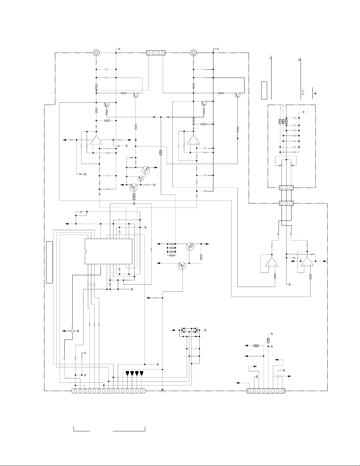
CR300
R411
100
1/2W
V+12A
EUR: 8274235006
USA: 8274235003
AUDIO PCB ASS'Y
V+5A
C424
C411
C410
C409
1500P
MBA
PCH1128
PCH1122
0.1
IC401
D/A BLOCK
JA401 (1/2)
PKB1029-
L ch
0
100P
(L405)
R1405
CH
C429
MBA
0.001
C427
470
R431
Q405
470
2SC3068
R429
NJM4580D
IC404 (2/2)
8
6
R416
10K METAL
GNDA
(220/25)
(1000/16)
YF
28272625242322212019181716
ML/IIS
MC/DM1
LRCK
DIN
123456789
R453 0
R451 0
R452 0
GA
C425
7
C422
MD/DM0
BCKIN
47/50
5
R426
R424
R422
47/50
XMUTE
CLKO
4
1.8K
GA
MODE
XTI
470
R433
22K
R427
C434
1500P
MBA
10K
1.8K
R411
METAL
MBA
C432
3300P
1K
22K
R439
XCS
XRST
ZERO
VCC2L
PE8001A
XTO
DGND
VDD
VCC2R
(220/25)
PCH1128
C405
GNDS
270
R435
R412
100
1/2W
C412
(220/25)
PCH1128
V+5A
Q403
DTA124EK
0.1
C408
YF
(4.7/50)
C407
PCH1127
15
NC
EXTL
VOUTL
AGND2L
D/A CONVERTER
AGND2R
EXTRNCVOUTR
1011121314
C406
(4.7/50)
PCH1127
10
YF
0.1
C404
Q407
2SC3068
V-12A
GNDA
C441
R445
VCC1
AGND1
R437
4.7/50
ZA
47K
L402
GNDD
470
R448
D403
1SS254
47
R447
QTL1015
J810
PDE1301 (1/2)
123
D401
1SS254
Q404
DTC124EK
Q409
4.7K
DTA114TK
R446
GNDA
10K
R420
V+5A
L404
GNDA
2.2K
V-12A
V+AU
V+5A
R406
4
QTL1015
10K
10K
10K
10K
D402
1SS254
R444
R443
R442
R441
C423
1500P
MBA
R415
Q401
DTC124EK
JA401 (2/2)
R1406
R432
R430
GA
C426
1
8
2
10K METAL
C421
Q402
DTA114EK
PKB1029-
R ch
0
(L406)
470
Q406
2SC3068
470
47/50
4
3
1.8K
R425
1.8K
R423
1K
R421
47/50
R440
100P
CH
C430
MBA
0.001
C428
R434
R428
22K
NJM4580D
IC404 (1/2)
C433
1500P
10K
R413
C431
3300P
22K
R438
2.7K
470
MBA
METAL
MBA
V-AU
R436
GNDS
: 1/4W
Ceramic CCSQSH
Ceramic CKSQYF
Ceramic CKSQYB
Film CCMBA
Electrolytic CEGA
Electrolytic CEZA
CAUTION
CHYFYB
MBAGAZA
270
Q408
2SC3068
470
R466
D404
1SS254
CAPACITOR unit w/o indication: F
JACK
RKN1002-A
HEADPHONE
(FROM SERVO)
CR401 (1/2)
RCV1123
(FROM AUDIO)
L408
47
R478
IC406 (1/2)
M5218AFP
7
8
4
6
5
R476
Electrical capacitor w/o indication CEAT
JA403
L461
QTL1015 x 3
4
CN403
CN401
1K
L463
L462
1
5
L ch INPUT
GAUD
123
123
QTL1015
YF
CH
YF
YF
CH
YF
CH
1
2
3
R ch INPUT
L407
QTL1015
C471
PCH1124
V+12A
GAUD
C468
C466
C465
C464
C463
C462
C461
(47/50)
: Chassis GND
Wattage w/o indication: 1/10W
RESISTOR unit w/o indication:
VR401 (2/2)
GNDS
OTHERS
GNDS
0.047
100P
0.01
0.01
100P
0.01
100P
8274239000
HEADPHONE PCB ASS'Y
47
R477
C472
PCH1124
(47/50)
IC406 (2/2)
R475
M5218AFP
4
3
V-12A
1K
7
8
2
44
IC402
TC7SU04F
R454 0
R456 0
GNDD
GNDS
YF
0.01
GNDD
GNDD
DALRCK
DADATA
from ENCODE IC
from ENCODE IC
from ENCODE IC
R455 0
987654321
10
DI
CL
XDLAT
DABCK
from ENCODE IC
LRSTD
from MODE COM
from MODE COM
from IC 357
from MECHA COM
CN301
SERVO_DIGITAL
XAMUTE
from ATIP DEC IC
ADSTBY
ADBCLK
ADDATA
ADLRCK
from ENCODE IC
to ENCODE IC
from ENCODE IC
from ENCODE IC
C403
0.047
V+5D
GNDD
YB
J407B
CN8101
INPUT
4
V+5A
5
3
2
0
0
R405
R457
C454
1514131211
J801
GNDD
6-3. AUDIO, HEADPHONE & VOLUME PCBs
6-3-1. AUDIO (DA BLOCK) & HEADPHONE PCBs
D406
DAN202K
D407
1SS355
D405
D408
C415
C414
C413
1SS355
DAP202K
CH
CH
YB
100P
100P
1000P
GNDD
V+5D
V+5A
V+AU
L401
L801
QTL1015
VTH1020
V-AU
GNDA
8765432
CN402
J31
POWER
GNDD
V+12
C883
GNDA
GNDA
YB
YB
V-12
0.1
0.1
C884
1
Page 45

EUR: 8274235006
USA: 8274235003
AUDIO PCB ASS'Y
V+5A
DAN202K
D803
CR300
(1/2)
AUDIO
from ENCODE IC
to ENCODE IC
from ENCODE IC
ADDATA
ADBCLK
0
D801
from ENCODE IC
ADLRCK
MCK
from ENCODE IC
MCK
R832
DAN202K
0.1
ADSTBY
YF
C831
4.7/50
YF
C832
0.1
C834
YF
10/50
C833
C846
1
2
3
4
5
6
7
8
9
10
11
12
13
14
0.01
VA+
NC
NC
PD
L/R
AINL+
AINL-
AGND
TST1
TST2
VREFIN
SEL18
CMODE
SMODE
470
R827
IC801
AK5340-VS
A/D CONVERTER
GAUD
AINR+
AINRVREF
NC
VDB+
NC
TST4
TST3
CLK
DGND
VDP+
FSYNC
SDATA
SCLK
28
27
26
V+5A
25
24
0.1
23
YF
22
C847
21
20
0.1
C836
19
YF
18
17
16
15
10/50
C835
DAP202K
820P
YB
C819
R823
C813
300
22/50
C823
47K
47K
R825
R821
8
CH
10K
12P
R813
2
R811
A/D BLOCK
CH
R809
2
8
6
6.8K
1
8
3
R855
C851
22/50
L329
QTL1015
JA801 (1/2)
PKB1029
L ch
7
4
5
NJM4558D
IC805 (1/2)
4
2.7K
100P
C821
(1/2)
YF
100K
R853
470K
R851
CH
NJM4565D
IC803
V-12A
0.01
C857
CN803
R801
100 (1/2W)
RS1/2LMF101J
V+12A
120P
C803
YF
0.01
GNDS
C855
V+12A
7
NJM4558D
IC805 (2/2)
5
6
GNDS
6-3-2. AUDIO (AD BLOCK) & VR PCBs
D804
300
R819
22/50
C844
1
4
NJM4565D
IC803 (2/2)
4.7K
R833
3
10/50
C817
10K
0.1
C815
YF
10K
10K
R815
R802
GNDS
R817
0.01
C807
YF
47/50
C811
47/50
C805
100 (1/2W)
RS1/2LMF101J
V-12A
YF
0.01
C809
2.7K
R807
VRL IN
VRL OUT
GNDA
8765432
IC804 (2/2)
4.7K
R834
10/50
C818
0.1
C816
YF
10K
R818
0.01
C806
YF
47/50
C811
47/50
C812
YF
0.01
C810
C805, C806, C811, C812: PCH1124
GNDA
VRROUT
CN8004
INPUT
D802
NJM4565D
VRRIN
1
DAP202K
300
R820
C848
1
4
3
R812
V+12A
22/50
8
10K
V+12A
YB
R814
2
10K
R816
2.7K
R808
820P
C820
47K
47K
R826
CH
10K
C824 12P
7
IC804 (1/2)
NJM4565D
8
RS1/2LMF101J
100 (1/2W)
R803
6
0.01 YF
C856
C852
22/50
L328
QTL1015
VRR IN
J1801 (2/2)
PKB1029
R824
R822
C814
5
R856
3
R ch
300
Ceramic CCSQSH
Ceramic CKSQYF
CAUTION
CHYFYB
22/50
R804
100 (1/2W)
CH
C804
YF
IC806 (1/2)
120P
0.01
C858
NJM4558D
6
RS1/2LMF101J
V-12A
GNDS
V-12A
7
NJM4558D
IC806 (2/2)
5
GNDS
4
6.8K
R810
1
8
4
2
100K
2.7K
R854
470K
R852
CH
100P
C801
CAPACITOR unit w/o indication: F
VR801 (1/2)
PCS1016-
10K
R881
VRR IN
VRROUT
8765432
CN805
: 1/4W
Ceramic CKSQYB
RESISTOR unit w/o indication:
Electrical capacitor w/o indication CEAT
J851
DE007WCO
VRLOUT
CN8005
INPUT
: Chassis GND
Wattage w/o indication: 1/10W
GNDS
OTHERS
GNDS
GNDS
GAUD
8274240000
VR PCB ASS'Y
GAUD
VR801 (2/2)
PCS1016-
10K
R882
VRLIN
1
45
Page 46

CR300
V+12RO
L8111
QTL1015
D8103
1SS355
Q8103
R8175
1
8
RSR1029
RY8101 (1/3)
2SD2114K (VW)
L8109
QTL1015
100K
R8129
GAUD
47K
C8101
CH
R8169
47P
R8125
300
300
C8105
2
L8103
R8149
100/25
R8141
QTL1015
3
0
1
3
47K
R8127
PKP1013
2
RY8101 (2/3)
4
300
R8159
NP
IC8105 (1/2)
NJM4558MD
V+12RO
47K
C8113
100P
JA8101
47K
R8131
47K
CH
3
R8153
1.2K
R ch
2
1
R8157
R8137
4
R8167 1.2K
QTL1015
47K
R8155
R8161
47P
C8103
CH
47K
R8133
L8105
5
300
C8107
8
6
7
6
100/25
R8143
7
47K
C8111
CH
0
RY8101 (3/3)
300
R8151
R8171
NP
0
IC8105 (2/2)
NJM4558MD
4
5
47K
R8135
100P
R8189
300
R9107
47K
R8139
V-12RO
R8063 0
0
GS
R8062
CH
100P
C8112
0
R8190
0
0
R9108
RY8102 (3/3)
300
R8152
300
R8172
C8108
100/25
0
V-12LO
4
IC8106 (2/2)
NJM4558MD
47K
5
R8140
47K
R8136
6
7
7
NP
R8144
L8106
5
R8162
V+12LO
8
6
QTL1015
300
47K
R8134
L ch
4
C8104 47P
2
1
47K
R8156
R8138 47K
CH
CH
3
100P
1.2K
R8158
C8114
JA8102
PKP1013
R8186 1.2K
RY8102 (2/3)
4
47K
R8154
300
R8160
C8106
IC8106 (1/2)
NJM4558MD
47K
R8132
47K
R8128
2
3
100/25
0
3
L8104
QTL1015
V+12LO
R8150
300
NP
R8142
1
2
R8170
C8102
R8126
QTL1015
Q8104
2SD2114K (VW)
D8104
L8110
GAUD
R8176
100K
: Chassis GND
GNDS
OTHERS
: RN1/10SEMETAL RESISTOR
1
8
1SS355
L8112
R5R1029
QTL1015
300
RY8102 (1/3)
CH
47K
47P
R8130
47K
V+12RO
V-12RO
V+12LO
YF
YF
C8121
0.1
C8119
0.1
C8117
PCH1128
(220/25)
C8115
PCH1128
(220/25)
0
0
R8191
R8193
V+12
GND
V-12
J8006
CN8005
R9211
QTL1015
Q8003
2SD2114K (VW)
L8023
GAUD
R8037
1%
5.6K
R8025
1%
R8024
7
8
6
R8017
Q8001
2SD2114K (VW)
GAUD
QTL1015
L8021
22K
R8035
4
RY8001 (2/3)
C8003
0
4
R ch (CH1)
BALANCED IN
JA8001
C8011
8
2
5.6K
4
5
36K
2
3
NP
22/50
R9005
R9017
PKP1011
1
100/25
1
IC8003 (1/2)
1%
3.9K
1
2
L8030
V+12
D8003
D8001
1SS355
8
5
1SS355
QTL1015
5
2
VSR1006
RY8003 (1/2)
7
4
6
IC8003 (2/2)
1
8
RSR1029
RY8001 (1/3)
6-4. INPUT PCB
V-12LO
YF
YF
C8122
0.1
C8120
0.1
C8118
PCH1128
(220/25)
C8116
PCH1128
(220/25)
0
0
R8194
R8192
1 2 3
CN805
VR
VRRIN
GNDA
VRROUT
GNDA
GNDA
1234567
0
0
R9215
3
6
RY8003 (2/2)
0
R8081
V+12
0
R8083
V-12
4
3
1%
5.6K
R8015
NJM4558MD
5.6K
R8023
1
IC8001 (1/2)
NJM4558MD
3
2
NJM4558MD
100K
R8011
1%
2.7K
470K
R8001
0
GAUD
3
R8007
R8043
100K
R8019
R8013
6
C8005
R8003
470K
7
1%
3.9K
0
R8041
5
R8009
NP
36K
22/50
0
IC8001 (2/2)
R8005
R8117
IC8103 (1/2)
V+12RO
IC8101 (2/2)
GAUD
VRLOUT
R9212
0
R9218
(47/50)
PCH1124
C8009
(47/50)
PCH1124
R8034
C8007
0
0
R8030
0
R8033
0
R8029
1%
RY8001 (3/3)
L ch (CH1)
GS
CH
C8127
12K
NJM4558MD
8
6
NJM4558MD
IC8101 (1/2)
NJM4558MD
GNDA
VRLIN
8
0
(47/50)
PCH1124
C8010
(47/50)
PCH1124
C8008
GAUD
GAUD
IC8002 (1/2)
NJM4558MD
3
36K
R8020
7
5
6
RY8002 (2/3)
NP
22/50
C8006
0
R8042
47P
2
R8113
7
2
V+12
1
1%
3.9K
R8010
1
3
10K
4
5
R8105
1
3
R8101
0
R9217
0
R8084
1%
5.6K
R8016
R8024
2
1%
100K
R8014
470K
R8004
0
R9006
0
4
C8123
V+12RO
10K
R8123
R8115 5.6K
V-12RO
R8109 36K
R8107 2.7K
10K
47K
R8103
QTL1015
470
L8101
PIN RIN
RGND
1234567
R9216 0
CN8004
R9213 0
10K
R8090
R9220
3
6
1
RY8004 (2/3)
0
C8012
100/25
R8082
7
V-12
8
4
5
6
5.6K
5.6K
R8022
IC8004 (2/2)
NJM4558MD
4
5
1%
36K
R8018
100K
R8012
2
3
4
1%
1%
3.9K
2.7K
R8008
R8006
NP
C8004
470K
R8002
R9018
GAUD
3
21
JA8002
PKP1011
CH
7
47P
8
6
10K
R8119
D8101 R8111
CN8101
VRROUT
0
R9221 0
1%
5.6K
R8026
1%
7
8
6
IC8002 (2/2)
NJM4558MD
V+12
RY8002 (3/3)
22/50
0
R8044
GS
IC8103 (2/2)
NJM4558MD
4
5
R8121
Q8101
2SC3068
1SS355 470
GAUD
CN803
AUDIO
RGND
LGND
RY8004 (1/2)
VSR1006
5
2
QTL1015
L8029
V-12RO
5.6K
L8201
QTL1015
GAUD
4 3 2 1
VRLOUT
LGND
R9219
D8004
1SS355 470
D8006 R8098
D8005 R8097
1SS355 470
2
RY8002 (1/3)
RSR1029
18
V+12
V+12
C8020
CN8003
L8231
QTL1015
(AUDIO PCB)
FROM J407A, B
PIN LIN
8
10K
R8089
0
Q8004
2SD2114K (VW)
1SS355
22K
R8038
GAUD
Q8010
2SC3068
GAUD
Q8009
2SC3068
1
3
Q8002
2SD2114K (VW)
D8002
1SS355
PCH1138
(1000/35)
YF
0.1
C8022
L8025
R9026
QTL1015
123
J32
V+5D
IC8004 (1/2)
22K
R8036
GAUD
3 2 1
3 2 1
C8021
YF
C8023
0
L8027
QTL1015
POWER
7
V-12LO
4
5
IC8104 (2/2)
NJM4558MD
5.6K
10K
R8122
Q8102
2SC3068
1SS355 470
GAUD
GAIN
GND
OUTPUT
12345
CN8006
GND
QTL1015
L8202 QTL1015
L8024
GAUD
10K
R8207
QTL1015
L8022
GAUD
L8009
V-12
J8005
(1000/35)
PCH1136
V-12
0.1
V+12LO
C8124
8
6
R8120
D8102 R8112
SEL
GAIN
OUTPUT
INPUT
L8203 QTL1015
L8204 QTL1015
L8205 QTL1015
R8201
R8202
R8203
V+12V+5D V+5D
V+5D
V+5D
V+5D
V+12
QTL1015
V-12
GND
J8006
CH
47P
10K
R8124
IC8102 (1/2)
NJM4558MD
R8104 47K
CN8102
REMOTE
FROM J708
(FUNCTION PCB)
10K
10K
10K
10K
R8204
10K
R8205
Q8006
DTA124TK
R8095
R8094
R8093
V+12
3 2 1
3
10K
R8116 5.6K
4
V-12LO
36K R8110
2.7K R8108
10K
3
470
R8102
L8102
QTL1015
1
J408
AUDIO
Q8201
10K
R8206
R8099
R8091
10K
3
1
R8096
10K
10K
10K
10K
Q8007
1
47P
C8128
2
R8114
7
8
5
R8106
1
2
2
Q8202
DTA124TK
22K
Q8005
2
DTC124TKA
CH
12K
R8118
IC8104 (1/2)
V+12LO
6
IC8102 (2/2)
NJM4558MD
GAUD
0
R4715
V-12
DTC124EK
2SD2114K (VW)
GAUD
10K
R8092
V-12
V+5D
NJM4558MD
47P
C3003
CH
CH
47P
C3002
R3002
110
L3013
QTL1015
AES/EBU IN
Q3704
2SA1037K (QRS)
B
47K
R3726
R3709
4.7K
0.01
C3715
YF
R3722
1.2K
Q3708
2SA1037K (QRS)
B
47K
R3730
R3713
4.7K
YF
C3719
0.01
0.1
C3708
YF
GNDD
C3709
(47/50)
PCH1124
L3704
QTL1015
47
432
IC3001
567
330
V+5D
V+5D
SN75157P
CH
R3003
R3001
3
R3717
DA204K
D3702
0.01
C3714
DA204K
D3708
0.01
C3718
C3007
330
GNDD
GNDD
2
1
4.7K
1
8
L3012
R3731
R3725
R3729
L3708
4.7K
47K
4.7K
V+5D
QTL1015
4
C3001
YF
YF
560
47K
R3708
YF
1.8K
R3712
YF
0.1
B
B
R3004
1K
0.01
C3005
YX
C3004
L3002
QTL1015
JA3001
PKP1011
0
R8053
C8024
GNDD
R3716
Q3703
2SA1037K (QRS)
V+5D
GNDD
DA204K
D3703
0.01
C3713
R3721
Q3707
2SA1037K (QRS)
V+5D
GNDD
DA204K
D3707
0.01
C3717
Ceramic CCSQSH
CAUTION
CHYFNP
CAPACITOR unit w/o indication: F
CH
330P
C3006
GNDD
(47/50)
PCH1124
L3011
QTL1015
V+5D
GNDS
DIN
123
GNDS
CN3002
CN302
SERVO_DIGITAL
R3715
820
1K
Q3702
2SA1037K (QRS)
Q3701
B
V+5D
47K
R3724
R3707
GNDD
4.7K
DA204K
47K
D3702
R3723
R3706
YF
4.7K
0.01
C3712
YF
R3720
3K
Q3706
2SA1037K (QRS)
Q3705
B
V+5D
47K
R3728
R3711
GNDD
4.7K
DA204K
47K
D3706
R3727
R3710
YF
4.7K
0.01
C3716
CN3702
RKN1030
0
C3720
YF
7
9
6
0.1
L3707
L3705
Ceramic CKSQYF
Electrolytic CENP
GNDD
R3714
2SA1037K (QRS)
B
R3719
5.1K
2SA1037K (QRS)
B
3
8
1
R8076
YF
Wattage w/o indication : 1/10W
Capacitor w/o indicaton 2125 Type
Electrical capacitor w/o indication CEAT
RESISTOR unit w/o indication:
EUR: 8274234006
USA: 8274234003
V+5D
GNDD
DA204K
D3701
L3705 - L3712: QTL1015
V+5D
GNDD
L3711
L3712
D3705
5
4
DA204K
2
L3709
L3706
L3710
GNDS
46
Page 47

R771 47K
R770 47K
AES/EBU
23456
6 7 8 9 10
OPT
ROTARY SW
S720
PSB1007
5 4 3 2 1
COAX
XLR +8
XLR -4
LINE
7
V701 PEL1097- PNB1285- FL HOLDER
V+5D
FSC/XTHR
XVCO
CS
REMCON
M
REQ
XPFAIL
UNLOCK
LREQ
M
ACK
XOPT
XRST
XFUSE
FSI
CN202
SERVO_DIGITAL
R769
47K
47K
R718
R717
34 35
CN701
47K
R716
FSCK
FSO
DEEM
GNDDF
C739
21 19 17 15 13 11 9 7 5 3 1
100/10
22 20 18 16 14 12 10 8 6 4 2
V+5D
47K
1K
772
R
V+5D
0
0
R753
R754
TEST MODE
0
0
R755
R756
R731
DCN1094-
10K
47K
702
R
GNDDF
K
S
G
G0
G1
G2
G3
G4
G5
G6
G7
G8
G9
G10
SK
SJ
SI
SH
SG
SF
SE
SD
SC
SB
SA
1 2 3 4 5 6 7 8 9 10 11 12 13 14 15 16 17 18 19 20 21 22 23 24 25 26
C712
47/16
0.01
100P
C701
CH
C702
YF
V+5D
GNDDF
D709
4.7K
R757
1SS355
V+5D
FINAL
Q705
8
R709 47K
R705 47K
K
C
41
42
43
44
45
46
47
48
49
50
51
52
53
54
55
56
57
58
59
60
61
62
63
64
SK
3
2
CR300
200 R752
200 R751
510 R750
D708
510 R749
GL3ED8
200 R748
2121
200 R747
33
510 R746
D707
47P
GND
IC705
VCCCSSK
0.1
C708
2
IC702
S-806E
CH
C715
GNDDF
GNDD
DTC124TK
V+5D
R736
SLP9118C51H
GREEN1
J703a
J703
GREEN1
V+5D
YF
0.1
4.7K
4.7K
R737
VSG1009- x 8
S717
S716 S718 S719
5
DI
DO
0.1
C710
YF
4
47K
R703
Q706
GNDDF
YF
SLP9118C51H
DISP OFF
470
D706
R740
D705
470
R739
TRACK INC.
S715
MENU
S714
SKIP PLAY
S713
CLEAR
SKIP ID
SET
S712
47K
R729
876
NC
0
R
7
3
z
H
1014
S
701
S
X
V
4.19M
A
M
X2
X1
SW1
LREQ
ROT4
UNLOCK
DIGOUT
XPFAIL
MREQ
REMIN
GND
ROT3
ROT2
ROT1
VDD
SCAN4
SCAN3
IC701
SCAN2
SCAN1
PE5056A9
SCAN0
KEYIN3
KEYIN2
KEYIN1
KEYIN0
ROT5
ROT6
SEG9
SEG8
SEG7
SEG6
SEG5
V-27
SI
SJ
SF
SH
SG
R711
100K
R759
100K
R758
1
0.1
C706
F
Y
+5D
V
100/10
C705
701
47K
R
VDD
VDD
GND
MODE
XOPT
MODE CONTROLLER
SEG4
SEG3
SEG2
SEG1
SEG0
GRID10
GRID9
SE
SB
SA
G9G8G7
SD
SC
G10
R712 R710
KI0
KI1
KS0
V-27V
S710
S703S702 S704
S706S705 S708
FSC/XTHR
25 26 27 28 29 30 31 32 33 34 35 36 37 38 39 40
24
XVCO
XRST
23
DEEMP
LDCE
22
XFUSE
21
GND
20
STANDBY LED
19
DISPLAY LED
18
XSRST
17
FSI
16
100
FSO
15
R728
FSCK
14
R727
RREQ
100
13
RACK
12
RSI
11
RSO
10
RSCK
9
VDD
8
GRID0
7
G0
GRID1
6
G1
GRID2
5
G2
GRID3
4
G3
GRID4
3
G4
GRID5
2
G5
GRID6
1
G6
GRID8
80 79 78 77 76 75 74 72 72 71 70 69 68 67 66 65
100K R713
ACN7081- x 6
KI2
KI3
KS1
KS2
REC
DIGITAL
SYNCHRO
S709S707 S711
TIME
OPEN/
VSG1009 x 10
R715
R714
V-27V
MUTE
RECORD
CLOSE
KI3
PYY1251
(BR93LC46AF)
V+5D
GNDDF
10K
R730
V+5D
RESET
SYSTEM
V+5D
NC
123
3
KI2
KI1
KI0
KS4
KS3
510 R745
GREEN2
RED1
RED2
12345
12345
RED1
RED2
GREEN2
Q701
Q702
Q703
Q704
DTA114EK x 4
181716151413121210
C709
VDD
XOE
47/10
C711
IC704
GND
DATA
123456789
ERASEWRITE
FINALIZE
(MANUAL)
TRACK INC.
AUTO/
MANUAL
GL3ED8
8274242000
FUNCTION B PCB ASS'Y
GNDDF
Q9Q8Q7Q6Q5
Q11
Q10
BU2092F
CLKCEQ0Q1Q2Q3Q4
GNDDF
0
R760
4.7K
R735
GNDDF
GND
OUTPUT GAIN
INPUT SELECT
INPUT GAIN
REMOTE
J709
CN8006
INPUT
up
LO
XLR
+4dBu
HI
pin
down
-8dBu
J709
OUTPUT GAIN
INPUT SELECT
INPUT GAIN
5 4 3 2 1
Vcc
OUT
GND
IC703 CP1U27X
6-5. FUNCTION PCB
J701
L701
2
1
QTL1015
123
GNDS
CN51
POWER
V-27
4
8274238000
FUNCTION A PCB ASS'Y
: Chassis GND
Wattage w/o indication: 1/10W
CAUTION
GNDS
RESISTOR unit w/o indication:
OTHERS
Ceramic CCSQSH
Ceramic CKSQYF
Ceramic CKSQYB
Ceramic CCSQSL
Ceramic CCSQCJ
CHYFYBSLCJ
CAPACITOR unit w/o indication: F
Electrical capacitor w/o indication CEAT
47
Page 48

CR300
J701
CN51
432
AC2
-27V
GNDS
EUR: 8274236006
USA: 8274236003
POWER PCB ASS'Y
R54
1.5K
R53
1.5K
R52
1.5K
R51
D54
MTZJ18B/C
10K
C52
C54
(100/50)
(220/25)
PCH1126
PCH1128
MA
C56
0.027
L11
VTH1020-
MA
C55
0.027
FUNCTION
1
AC1
TL
C13
0.01
CABLE HOLDER
51048-0600
12345
V+5A
V+5D
GNDA
L23
C25
PCH1129
HEAT SINK
PNS1043
C23
PCH1129
3
OUT
2
BA05T
1
IN
2
IC25
ICP-N15
ICP-N15
C24
0.047
YF
R21
8.2K
C21
10000/16
CN355
GNDD
VTH1020-
(470/50)
(470/50)
SERVO_DIGITAL
6
V+U
GNDU
KN12
1
J2
1
1
KN13
VNF1084
PDF1168
VNF1084
: 1/4W
: Chassis GND
GNDS
OTHERS
Wattage w/o indication: 1/10W
RESISTOR unit w/o indication:
CAUTION
Ceramic CKSQYF
Film CFTLA
Mylar CQSA
YFTLMA
Electrical capacitor w/o indication CEAT
CAPACITOR unit w/o indication: F
GNDS
C41
C37
J32
V+12A
PCH1138
(2200/25)
3
1
2
PCH1138
(2200/25)
10DF2FA9
D31 - D34:
123
GNDA
OUT
IC32
IN
CN8003
INPUT
V-12A
PNB1027
HEAT SINK
NJM79M12FA
IC22
IC21
PNS1015
HEAT SINK
ICP-N15
OUT
BA05T
IN
IC23
J21
IC24
3
1
CN402
AUDIO
CABLE HOLDER
51048-0800
J31
8765432
V-AU
V+5A
V+AU
GNDU
C42
PCH1122
(1000/16)
3
OUT
2
IC33
1
IN
NJM7805FA
R38
8.2
RFA1/4PL8R2J
3
OUT
2
IC31
BA05T
1
IN
PNS1015
HEAT SINK
TL
C11
0.01
GNDA
C40
C36
V+12A
PCH1137
(3300/35)
PCH1137
(3300/25)
GNDA
1
V-12A
D52
11ES2
0.1
C12
YF
FL
CN11
123456789
123456789
J11
FL
1A 125V
500mA 250V
AGAINST RISK OF FIRE,
REPLACE WITH SAME TYPE
REK1075-
FU1
USA
CN1
PKP1012-
FU1
FUSE
1
LIVE
2
NEUTRAL
3
PDF1198-
6-6. POWER & TRANSFORMER PCBs
AC INLET
GNDS
AND RATINGS OF FUSE.
AEK1051-
CAUTION- FOR CONTINUED PROTECTION
EUR
S1
RSA1001
L1
VTL1008
C3
ACG7020-
3
PW
C1
ACG7020-
4
PW
2
1
C2
ACG7020-
CN2
PW
2 1
51052-0900
CABLE HOLDER
J1
2 1
0.1
C901 - C909
8
D33
D31
YF
C31
1000P
R31
12
C35
PCH1127
(4.7/50)
C34
PCH1127
(4.7/50)
GND
AC1
AC2
AUA
GND
AUB
AC1
AC2
AUA
GND
YFYFYFYFYFYFYF
9
10111213141516
AUB
GND
4
1
D34
D32
MA
C33
0.022
MA
C32
0.022
SEA
SEB
J3
PDF1176
SEA
SEB
YF
YF
IC1
AEK7017
USA
EUR
PTT1355:
PTT1346:
HEAT SINK
PNS1064
D11
S2VB20F
YF
C17
YF
0.01
YF
C15
C16
0.01
0.047
GNDS
AGAINST RISK OF FIRE,
REPLACE WITH SAME TYPE
NO.49103.5 MFD.BY
LITTELGUSE INC. FOR IC1.
T1
CAUTION- FOR CONTINUED PROTECTION
8274241000
TRANSFORMER PCB ASS'Y
48
Page 49

6-7. LOADING A / B & SERVO MECH PCBs
CR300
CN501
CN601
SL-
SL+
SPDL+
SPDL-
TOCPOS
TERM
GNDA
VA+5
FG
SW1
1
SW2
2
SW3
3
L-
4
L+
5
LOADING MECHA PCB ASSY
SLIDER MOTOR
9
8
7
6
5
4
3
2
1
SPINDLE MOTOR
S501
VSK1011-
CN502
1
2
SERVO MECHA PCB ASSY
S601
PSG1013
4.7K
R602
CN551
2
1
LOADING MOTOR
LOADING MECHA B PCB ASSY
GNDA
VA+5
FG
3
2
1
3
2
1
J601
GNDA
VA+5
FG
MECH PCB ASSY
PC651 NJL5803K
R651
200
1
324
49
Page 50

CR300
7. GENERAL INFORMATION
7-1. IC
The information shown in the list is the basic one and may not correspond exactly to that shown in the circuit diagrams.
NJM2136M (SERVO DIGITAL PCB ASSY: IC101, Operational Amplifier)
• Pin Assignment
BAL
–INPUT
+INPUT
V–
1
2
3
4
8
BAL
7
V+
6
OUTPUT
5
NC
MC34072D (SERVO DIGITAL PCB ASSY: IC102, Operational Amplifier)
• Pin Assignment
Output 1
Input 1
Input 1
1
2
3
4
V
EE
• Block Diagram
8
V
7
Output 2
6
Input 2
5
Input 2
CC
V
CC
50
Inputs
Q1 Q3
Bias
–
+
Q2
Base
Current
Cancellation
R1
Q8 Q9
D1
R3
Q4 Q5 Q6 Q7 Q17
R2
C1
Q10 Q11
Q14
Q13
Q12
R4
R5
C2
D2
R6 R7
D3
Q16
Q15
Q18
Output
R8
Q19
Current
Limit
VEE/GND
Page 51

AK8563 (SERVO DIGITAL PCB ASSY: IC103, RF Processor IC)
• Pin Assignment
CR300
AVSS160NC(VSS)59WRF58OSTCC57SLLPFN56SLLPFP55TESTEQRFP
TESTEQRFN
PHO52BHO51AGND250AGC3C49AGC2C48AGC1C47ATFM46TESTAGC45AGCON44WLDON43XRST42AVDD2
54
53
41
AVDD1 61
RECDIN 62
RRF 63
MPXOUT 64
AUX1 65
AUX2 66
AUX3 67
GIN 68
HIN 69
EIN 70
FIN 71
HAVC 72
DIN 73
CIN 74
BIN 75
AIN 76
RREF 77
VRDCN 78
VRDC 79
AVSS3 80 DVDD21
1
2
3
4
5
6
7
8
FPDIN
AVDD3
FPDO
FVREF
WREF
VWDC
VWDCN
9TE10FE11
MPP
TEIN
12
13
BIAS
14
VREF
AGND1
15
NC(VSS)
16
17
XLAT
18
SCLK
SDATA
19
20
MCLK
AVSS240
WFPDSH39
RFPDSH38
WBLSH37
SPDSH36
MPDSH35
SLHOLD34
GAINUP133
GAINUP232
GAINUP331
XDECEFM30
DECEFM29
RZC28
RECD127
RECD226
TZC25
XTAND24
XTOR23
ATFG22
DVSS
• Block Diagram
HAVC
MPDSH
AIN
BIN
CIN
DIN
SPDSH
EIN
FIN
GIN
HIN
WBLSH
GAINUP1
WLDON
RFPDSH
WFPDSH
FPDO
FPDIN
FVREF
WRF
58
72
35
76
75
74
73
36
70
71
68
69
37
33
43
38
39
SH
MATRIX
78
VRDCN
79
77
VRDC
APC
RREF
7
6
VWDCN
VWDC
4
2
3
SLHOLD56SLLPFN55SLLPFP62RECDIN
34
29
SRFO
RFO
FEO
MPP
SPPO
ADO
BCO
SADBC
RFOM
WRF
5
14
13
VREF
WREF
AGND150AGND2
DECEFM30XDECEFM63RRF28RZC27RECD126RECD257OSTCC53TESTEQRFN
RF_EQUALIZER
TESTEQRF
RRF
60
61
19
45
12
BIAS
MCLK
AVDD1
TESTAGC
41
AVSS1
AVDD2
40
1
AVSS2
TESTEQRFP11FE10TE
54
RRF
FE
TE
ATFM
VRDC
VWDC
VREF
20
21
80
DVSS
DVDD
AVSS3
AVDD3
MPP
8
15
NC(VSS)
59
NC(VSS)
FOCUS &
TRACK
ATIP
P/H & B/H
MPX
REGVREF
9
TEIN
25
24
23
44
32
31
46
22
47
48
49
52
51
65
66
67
64
17
18
16
42
TZC
XTAND
XTOR
AGCON
GAINUP2
GAINUP3
ATFM
ATFG
AGC1C
AGC2C
AGC3C
PH0
BH0
AUX1
AUX2
AUX3
MPXOUT
SDATA
SCLK
XLAT
XRST
51
Page 52

CR300
• Pin Function
No.
1I 142DDVAI nipylppusrewopevitisopgolanA
AVDD3
2I 24TSRXI
FPDIN Laser monitor diode connection pin
3I 34NODLWI
FVREF
4O/I44NOCGAI
FPD0
5I 54CGATSETOniptseT
WREF Power setting voltage input for Write APC
6O 64MFTAO tuptuolangiselbboW
VWDC
7I 74C1CGAO
VWDCN
8O 84C2CGAO
MPP
9I 94C3CGAO
TEIN
01O 052DNGAO egatlovecnereferlanretnirofnipgnilpuoceD
TE
11O 150HBO langisFRRfotuptuolevel-mottoB
FE
21O 250HPO langisFRRfotuptuolevel-kaeP
BIAS
31O 35NFRQETSETOniptseT
AGND1
41O/I45PFRQETSETOniptseT
VREF
51 55PFPLLSI
NC (VSS)
61I 65NFPLLSI
XLAT
SDATA
71I 75CCTSOO
SCLK
81I 85FRWO tuptuolangisFRetirW
91I 95)SSV(CNSSVottcennoC
MCLK
DVSS
02I 061SSVAO nipdnuorggolanA
12I 161DDVAI nipylppusrewopevitisopgolanA
DVDD
22O 26NIDCERI noitcetedkcolbgnidrocerroftupniFR
ATFG
XTOR
32O 36FRRO tuptuolangisFRdaeR
42O 46TUOXPMO rotinomlangisroftuptuorexelpitluM
XTAND
TZC
52O 561XUAI rotinomlangisrof)1(tupniyrailixuA
62O 662XUAI rotinomlangisrof)2(tupniyrailixuA
RECD2
72O 763XUAI rotinomlangisrof)3(tupniyrailixuA
RECD1
82O 86NIGI tupni)G(langismaebediS
RZC
92O 96NIHI tupni)H(langismaebediS
DECEFM
03O 07NIEI tupni)E(langismaebediS
XDECEFM
13I 17NIFI tupni)F(langismaebediS
GAINUP3
23I 27CVAHI slangismaebedisdnaniamfotupniegatlovretneC
GAINUP2
GAINUP1
33I 37NIDI tupni)D(langismaebniaM
43I 47NICI tupni)C(langismaebniaM
SLHOLD
53I 57NIBI tupni)B(langismaebniaM
MPDSH
63I 67NIAI tupni)A(langismaebniaM
SPDSH
73HSLBWI
83HSDPFRI
93HSDPFWI
042SSVAI nipdnuorggolanA083SSVAI nipdnuorggolanA
I/O FunctionPin Name
Analog positive power supply pin
Reference voltage input for APC
Laser monitor output (connect a resistor for I/V
conversion between this pin and FPDIN (pin 2))/
Laser monitor voltage input
Laser driver control output for Write
Laser driver control amp. (-) for Write
Main push-pull signal output
Input for tracking signal process
Tracking error signal output
Focus error signal output
Connect a bias resistor. RBIAS = 4.7kΩ
Decoupling pin for internal reference voltage
Decoupling pin for internal reference voltage /
Reference voltage input
Connect to VSS
Latch input for register setting
Data input for register setting
Clock input for register setting
Main clock input (34.5744MHz)
Digital ground pin
Digital positive power supply pin
ATIP FG output (Wobble signal after the binary data
conversion)
Tracking amplitude detection output
Tracking error detection output
Tracking zero-cross detection signal output
Recording block detection signal 2
“H”: Recording block, “L”: Unrecording block
Recording block detection signal 1
“H”: Recording block, “L”: Unrecording block
RF zero-cross detection signal output
EFM output after sliced (inversion)
EFM output after sliced (positive-phase)
0 and + 18 dB switching control input
“H”: + 18 dB, “L”: Hold
Slice level hold signal input “H”: Hold
Sample pulse input for main-beam
“H”: Sample, “L”: Hold
Sample pulse input for side-beam
“H”: Sample, “L”: Hold
“H”: Sample, “L”: Hold
“H”: Sample, “L”: Hold
“H”: Sample, “L”: Hold
langiselbboWroftupnieslupelpmaS
CPAdaeRroftupnieslupelpmaS
CPAetirWroftupnieslupelpmaS
.oNemaNniPO/InoitcnuF
Register reset “L”: Initialize the register
“L”: Set Write APC set-value to zero, “H”: LD ON
“H”: AGC ON, “L”: AGC reset
LPF input (+) for auto slice
LPF input (-) for auto slice
-
77FERRI CPAdaeRroftupniegatlovgnittesrewoP
87NCDRVI
97CDRVO daeRroftuptuolortnocrevirdresaL
Laser driver control amp. (-) for Read
tupnilortnocDLetirW
tupnielbaneCGAelbboW
esnopserCGArofnipnoitcennocroticapaclanretxE
gnittesdeeps
rezilauqefognittescfrofnipnoitcennocroticapaC
rellecnac-tesffotuptuo
52
Page 53

BA7082F (SERVO DIGITAL PCB ASSY: IC302, VCO IC)
1
O
9
201
311
4WB
I
21
531I
6I 41O
7O 51
I
861
Collector open output
Logic block output for control sensitivity
adjustment
Logic block input for control sensitivity
adjustment
Logic block input for control sensitivity
adjustment and 1/2 frequency demultiplier
switch H: through, L: 1/2 frequency
demultiplier output
GND pin
VCO output pin
VCO control pin. Normally, use for shortcircuit with VO (pin 14).
Capacitor connection pin for VCO oscillation
Amp. input for sensitivity adjustment
IN1: positive-phase input IN2: Inverting input
Amp. output for sensitivity adjustment
VCC pin
f0 Adjust pin
V0
VCTL
VCC
FADJ
FOUT
1/2FB
SW2
SW1
-
IN2
CT1
CT2
GND
BWB
SW3
-
-
-
IN1
FunctionI/ONo. Pin Name FunctionI/ONo. Pin Name
• Block Diagram
IN1
16
IN2
15
VO
14
VCTL
13
CT1
12
CT2
11
VCC
10
CR300
F
ADJ
9
• Pin Function
1
SW1
2
SW2
3
SW3
4
BW
5
BWB
VCO
6
1/2FB
7
FOUT
1/2
SW
8
GND
AD1893JST (SERVO DIGITAL PCB ASSY: IC311, Sample Rate Converter IC)
• Block Diagram
NC43DATA_I42XTAL_I41NC40XTAL_O39NC38SETSLW
44
1
NC
LR_I
NC
VDO
GND
NC
NC
2
3
4
5
6
7
8
9
10
11
BCLK_I
WCLK_I
BKPOL_I
MODE0_I
12
SERIAL IN
ACCUM
MULT
FIFO COEF ROM
NC
13
14
CLOCK
TRACKING
15NC16
GND
17NC18
RESET
MODE1_I
PWRDWN
BCLK_O34NC
37NC36
35
SERIAL OUT
19NC20
21
MUTE_I
22
NC
MUTE_O
MODE1_O
33
NC
32
WCLK_O
31
LR_O
30
DATA_O
29
NC
28
VDO
27
GND
26
NC
25
BKPOL_O
24
MODE0_O
23
NC
53
Page 54

CR300
• Block Diagram
BA5912AFP-Y (SERVO DIGITAL PCB ASSY: IC351, Driver IC)
IN1'24IN123OP2-OUT22OP2-IN–21OP2-IN+20BIAS
25
10kΩ
10kΩ
LEVEL
SHIFT
Vref1 Vref1 Vref2 Vref2
REF1
SWITCH
CH1
10kΩ
10kΩ 10kΩ
MUTE
1
2
3
4
5
GND
MUTE1
REF1
OUT1–
Pow Vcc1
T.S.D.
10kΩ 10kΩ
10kΩ 10kΩ
6
OUT1+
GND18OP1-IN+17OP1-IN–16OP1-OUT15IN214IN2'
19
LEVEL
SHIFT
10kΩ
7
8
9
10
11
GND
OUT2–
OUT2+
Pow Vcc2
REF2
SWITCH
12
Pre Vcc
10kΩ
10kΩ
CH2
MUTE
REF2
13
MUTE2
• Pin Function
1
GND
2
MUTE1
3
REF1
4
Pow Vcc1
5
OUT1-
6
OUT1+
7
GND
8
OUT2+
9
OUT2-
10
Pow Vcc2
11
Pre Vcc
12
REF2
13
MUTE2
Sub-straight GND
CH1 mute pin
CH1 Vref switching pin
Pow Vcc (CH1)
CH1 negative output
CH1 positive output
Sub-straight GND
CH2 negative output
CH2 positive output
Pow Vcc (CH2)
Pre Vcc
CH2 Vref switching pin
CH2 mute pin
FunctionNo. Pin Name
14
15
16
17
18
19
20
21
22
23
24
25
IN2'
IN2
OP1 -OUT
OP1 -IN OP1 -IN +
GND
BIAS
OP2 -IN+
OP2 -INOP2 -OUT
IN1
IN1'
CH2 input pin for gain adjustment
CH2 gain fixed input
OP amp. 1 output
OP amp. 1 - input
OP amp. 1 + input
Sub-straight GND
Bias input
OP amp. 2 + input
OP amp. 2 - input
OP amp. 2 output
CH1 gain fixed input
CH1 input pin for gain adjustment
FunctionNo. Pin Name
54
Page 55

BA5932FP (SERVO DIGITAL PCB ASSY: IC352, Driver IC)
1
2
3
4
5
6
7
8
9
10
11
12
13
14
MUTE
OPIN1 1+
FWD1
REV1
OPIN1 1OPOUT1 1
OPIN1 2GND
OPOUT1 2
SW
OUT1OUT1+
REV
LDOUT-
Mute pin
OP amp. non-inverting input
Forward input
Reverse input
Op amp. inverting input
OP amp. output
OP amp. inverting input
Sub-straight GND
OP amp. output
Analog switch input
Driver output
Driver output
Loading reverse input
Loading negative output
15
16
17
18
19
20
21
22
23
24
25
26
27
28
LDVcc
LDOUT+
FWD
OUT2+
OUT2OPOUT2 2
Vcc
OPIN 2 2
OPOUT2 1
OPIN2 1REV2
FWD2
OPIN2 1+
VREF
Vcc for loading and output H bridge section
Loading positive output
Loading forward input
Driver output
Driver output
OP amp. output
Vcc for two axes driver and loading pre section
OP amp. inverting input
OP amp. output
OP amp. inverting input
Reverse input
Forward input
OP amp. non-inverting input
Reference voltage output
No. Pin Name Function
No. Pin Name Function
• Block Diagram
21
Vcc
8
CC
V
Vcc
VREF27OPIN21+26FWD225REV224OPIN21–23OPOUT2122OPIN22
28
10kΩ 10kΩ
10kΩ 10kΩ
10kΩ
10kΩ
10kΩ
10kΩ
Driver⋅Mute
1
2
3
4
5
6
7
OPOUT2219OUT2–18OUT2+17FWD16LDOUT+15LDV
20
× 1
10kΩ
10kΩ
9SW10
TSO
Switch
⋅
Analog
× 1
× 1
11
× 1
12
LOADING
Vcc
FWD OUT
LOADING
REV OUT
13
CR300
CC
14
MUTE
OPIN11+
• Pin Function
FWD1
REV1
OPIN11–
OPOUT11
GND
OPIN12–
OPOUT12
OUT1–
OUT1+
REV
LDOUT–
55
Page 56

CR300
• Pin Assignment
CXD2585Q (SERVO DIGITAL PCB ASSY: IC353, Digital Signal Processor IC)
ASYI
RFAC
49
12
XPCK
XUGF
48
13
ASYO
47
14
GFS
C2PO
0
DD
AV
IGEN
46
15
SCOR
45
16
0
SS
AV
44
17
C4M
ADIO
18
0
SS
DV
WDCK
19
TE42CE43RFDC
41
20
MIRR
COUT
40
39
38
37
36
35
34
33
32
31
30
29
28
27
26
25
24
23
22
21
SE
FE
VC
TES1
TEST
DVSS1
FRDR
FFDR
TRDR
TFDR
SRDR
SFDR
DVDD1
FSTO
SSTP
MDP
LOCK
PWMI
FOK
DFCT
DVDD2
ASYE
MD2
DOUT
LRCK
PCMD
BCK
EMPH
XTSL
DVSS2
XTAI
XTAO
SOUT
SOCK
XOLT
SQSO
SQCK
SCSY
SBSO
EXCK
1
DD
AV
BIAS
VCTL
V16M
VPCO
58
59
60
61
62
63
64
65
66
67
68
69
70
71
72
73
74
75
76
77
78
79
80
1
2
3
0
DD
XRST
MUTE
DV
57
4
56
5
DATA
6
XLAT
54
CLOK7SENS
FILO
FILI55PCO
53
8
SCLK9ATSK
52
CLTV
51
10
1
SS
AV
50
11
WFCK
• Block Diagram
FSTO
C4M
RFAC
ASYI
ASYO
ASYE
BIAS
XPCK
FILO
FILI
PCO
CLTV
MDP
LOCK
PWMI
SENS
DATA
XLAT
CLOK
SCOR
SBSO
EXCK
SCSY
SQSO
SQCK
RFDC
IGEN
XTAI72XTAO60VPCO
XTSL58VCTL
71
69
59
27
16
50
49
48
62
57
12
53
54
55
52
25
24
23
7
4
5
6
15
79
80
78
76
77
43
42
CE
41
TE
40
SE
39
FE
38
VC
46
Clock
Generator
Asymmetry
Corrector
Digital
Digital
Interface
OP Amp
Analog
Switch
PLL
CLV
CPU
V16M
A/D
Converter
XUGF13GFS68EMPH
11
EFM
Demodulator
Sub Code
Processor
Servo
Auto
Sequencer
10
WFCK
17
Error
Corrector
32k
RAM
SIGNAL PROCESSING
Servo
Interface
MIRR
DFCT
FOK
SERVO DSP
FOCUS
SERVO
TRACKING
SERVO
SLED
SERVO
WDCK14C2PO65LRCK
PCMD66BCK
67
D/A
Interface
Digital
OUT
SERVO BLOCK
PWM GENERATOR
FOCUS PWM
GENERATOR
TRAKING PWM
GENERATOR
SLED PWM
GENERATOR
MUTE
3
BLOCK
37
TES1
36
TEST
2
XRST
63
MD2
64
DOUT
73
SOUT
74
SOCK
75
XOLT
8
SCLK
19
COUT
26
SSTP
9
ATSK
20
MIRR
21
DFCT
22
FOK
33
FFDR
34
FRDR
31
TFDR
32
TRDR
29
SFDR
30
SRDR
56
44
ADIO
Page 57

• Pin Function
.oNemaNniPO/InoitcnuF.oNemaNniPO/InoitcnuF
1VDDD014ETI tupnirorregnikcarT
2TSRXI 24ECI tupnigolanaovresretneC
3ETUMI 34CDFRI tupnilangisFR
4ATADI 44OIDAO noitcennocnoNniptseT
5TALXI 54VA
6KOLCI 64NEGII reifilpmaPOroftupnitnerructnatsnoC
7SNESO 74VA
8KLCSI 84OYSAO
9KSTAO/I94IYSAI tupniegatlovetarapmocyrtemmysA
01KCFWO 05CAFRI tupnilangisMFE
11FGUXO 15VA
21KCPXO 25VTLCI esaercnilaudargroftupniegatlovlortnoc1OCV
31SFGO 35OLIFO )LLPlatigid=evalS(LLPretsamroftuptuoretliF
41OP2CO 45ILIFI LLPretsamroftupniretliF
51ROCSO
61M4CO
71KCDWO
81VD
SS
0DNGlatigiD85LTCVI LLPMFEdnab-ediwroftupniegatlovlortnoc2OCV
91TUOCO/Ilangistnuocrebmun-kcartfotuptuodnatupnI95M61VO/I
02RRIMO/ItuptuodnatupnilangisrorriM06OCPVO LLPMFEdnab-ediwroftuptuopmupegrahC
12TCFDO/ItuptuodnatupnilangistcefeD16VD
22KOFO/ItuptuodnatupnilangisKOsucoF26EYSAI )NO:H,FFO:L(lortnocFFO/NOtiucricyrtemmysA
32IMWPI rotomeldnipsfotupnilortnoclanretxE362DMI )NO:H,FFO:L(lortnocFFO/NOtuolatigiD
42KCOLO/I46TUODO tuptuotuolatigiD
52PDMO rotomeldnipsfotuptuolortnocovreS56KCRLO sF=ftuptuokcolcRLecafretniA/D
62PTSSI tsomrennicsidfotupnilangisnoitceteD66DMCPO
72OTSFO nipLATXfoylpitlumedycneuqerf3/2stuptuO76KCBO tuptuokcolctiBecafretniA/D
82VD
DD
1ylppusrewoplatigiD86HPMEO
92RDFSO
03RDRSO 07VD
13RDFTO
23RDRTO 27OATXO tuptuotiucricnoitallicsolatsyrC
33RDFFO
43RDRFO 47KCOSO kcolbovresehtnituptuokcolctuodaeratadlaireS
53VD
SS
1DNGlatigiD57TLOXO kcolbovresehtnituptuohctalatadlaireS
63TSETI
731SETI 77KCQSI tuodaerOSQSroftupnikcolC
83CVI tupniegatlovretneC87YSCSI ROCSRGfosuonorhcnyserroftupnI
93EFI tupnilangisrorresucoF97OSBSO WotPbuSfotuptuolaireS
04ESI tupnilangisrorredelS08KCXEI tuodaerOSBSroftupnikcolC
• PCMD is an MSB first, two's complement output.
Notes)
• GTOP is used to monitor the frame sync protection status. (High: sync protection window released)
• XUGF is the negative pulse for the frame sync derived from the EFM signal. It is the signal before sync protection.
• XPCK is the inverse of the EFM PLL clock. The PLL is designed so that the falling edge of XPCK and the EFM signal transition point coincide.
• GFS goes high when the frame sync and the insertion protection timing match.
• RFCK is derived with the crystal accuracy. This signal has a cycle of 136us.
• C2PO represents the data error status.
• XROF is generated when the 32K RAM exceeds the ±28 Frame jitter match.
-
Digital power supply
System reset. Rest when “L”
Mute input. Mute when “H”
Serial data input from CPU
Latch input from CPU
Serial data is latched at the falling edge.
Serial data transfer clock input from CPU
SENS output to CPU
CLock input for SENS serial-data readout
Input and output for unti-shock
WFCK output
XUGF output. MNT0 and RFCK output by
switching the command.
XPCK output. MNT1 output by switching the
command.
GFX output. MNT2 and XROF output by
switching the command.
C2PO output. MNT3 and GTOP output by
switching the command.
Outputs “H” when either subcode sync. S0 or S1 is
.detceted
sF2=ftuptuokcolcdroW
-
GFS is asmpled at 460Hz; when GFS is “H”, this pin
outputs “H”. If GFS is “L” eight consecutive samples,
this pint outputs “L”. Input when LKIN=“1”.
-
tuptuoevirddelS
tuptuoevirdgnikcarT
tuptuoevirdsucoF
-
DNGyllamron:nipTSET
hctiwsdnammocybROCSRGstuptuO
SS
0DNGgolanA
DD
0ylppusrewopgolanA
SS
1DNGgolanA
55OCPO LLPretsamroftuptuopmupegrahC
ylpitlumedycneuqerf4/1stuptuOtuptuozHM6332.4
65VA
DD
.hctipelbairavdnaedomW-VACehtniM61Vfo
1ylppusrewopgolanA
75SAIBI tiucricyrtemmysafotupnitnerructnatsnoC
DD
2ylppusrewoplatigiD
96LSTXI
SS
2DNGlatigiD
17IATXI
37TUOSO kcolbovresehtnituptuoatadlaireS
67OSQSO
-
EFM full-swing output (“L”=VSS, “H”=VDD)
-
-
hctiws
-
)tsrif
Outputs “H” when the playback disc has emphasis,
and “L” when there is no emphasis.
tupninoitceleslat'X
-
CR300
LLPMFEdnab-ediwroftuptuonoitallicso2OCV
dnammocybLLP-MFEdnab-ediwroftupnikcolC
BSM,PMOCs'2(tuptuoatadlaireSecafretniA/D
H:zHM8868.33,L:zHM4439.61
tupnitiucricnoitallicsolatsyrC
.nipsihtaivkcolcretsamlanretxeehttupnI
tuptuoatadleveldnakaepMCP,tib-08QbuS
tuptuoatadTXETDC
57
Page 58

CR300
• Block Diagram
TK11041M-1 (SERVO DIGITAL PCB ASSY: IC355, Thermo Sensor IC)
VCC
1
Temperature
Sensor
5
GND
× 1
S-806E (FUNCTION A ASSY: IC702, Voltage Detector IC)
• Block Diagram
1
DD
V
3
VO
3
OUT
VSS
2
58
Page 59

PE8001A (AUDIO PCB ASSY: IC401, D/A Converter IC)
• Block Diagram
CR300
2L
CC
V
AGND2L9V
20
19
3
BCK
LRCK
DATA
ML/IIS
MC/DM1
MD/DM0
CS/IWO
MODE
MUTE
RST
Serial
1
Input
I/F
2
28
27
26
Mode
23
Control
I/F
24
25
22
SCK
8X
Oversampling
Digital Filter
with
Multi-level
Delta-Sigma
Modulator
Function
Controller
BPZ-Cont
Crystal OSC Power Supply
6
5
XTI
XTO
4
CLKO
DAC
DAC
15
1
CC
V
DD
V
7
8
14
AGND1
• Pin Function
No. Pin Name FunctionI/O
1KCRLI )sf(tupnikcolcKCRL511CCVV5+ylppusrewopgolanA
2ATADItupniataD61LTUOV
*1
3KCBI atadroftupnikcolctiB71CNnoitcennocnoN
*1
*1
4OKLCO kcolcmetsysfotuptuoreffuB81LTXE
5ITXI
tupnikcolc
6OTXO noitcennocnoitallicsolatsyrC02L2CCVV5+ylppusrewopgolanA
7DNGDDNGlatigiD12
8DDVV5+ylppusrewoplatigiD22
9R2CCVV5+ylppusrewopgolanA32
01R2DNGADNGgolanA42EDOM
-
-
-
-
11RTXEO nommoc.pmatuptuogolanahcR52
21CNnoitcennocnoN620MD/DM
31RTUOVO tuptuoegatlovgolanahcR721MD/CM
411DNGADNGgolanA82SII/LM
-
:etoN
*1
*2
*3
tupnireggirtttimhcS:
rotsiserpu-lluphtiwtupnireggirtttimhcS:
rotsisernwod-lluphtiwtupnireggirtttimhcS:
No. Pin Name FunctionI/O
lanretxeronoitcennocnoitallicsolatsyrC
91L2DNGADNGgolanA
OREZ
TSR
OWI/SC
ETUM
2R
OUT
Open drain
DGND
-
O
-
O
-
-
O
I
I
I
I
I
I
I
AGND2R
10
Low-pass
Low-pass
teseR
Filter
Filter
*2
16
V
OUT
L
18
EXTL
13
V
OUT
R
11
EXTR
21
ZERO
tuptuoegatlovgolanahcL
nommoc.pmatuptuogolanahcL
galfatadoreZ
*3
tcelestamroftupnI/tcelespihC
*2
tceleslortnocedoM
)erawdraH:L,erawtfoS:H(
*2
lortnocetuM
*2
1tcelessisahpmeed/atadlortnocedoM
*2
2tcelessisahpmeed/KCBlortnocedoM
tcelestamroftupnI/hctallortnocedoM
*2
59
Page 60

CR300
7-2. DISPLAY
PEL1097 (FUNCTION PCB ASSY: V701)
• FL TUBE
1 35
• Anode & Grid Assignment
60
Page 61

CR300
• Pin Assignment
61
Page 62

FOSTEX CORPORATION 3-2-35 Musashino, Akishima, Tokyo, Japan 196-0021
FOSTEX CORPORATION OF AMERICA 15431 Blackburn Ave., Norwalk, CA 90650, U.S.A.
© PRINTED IN JAPAN JUNE 1999 8288782000
 Loading...