

Page 1

Service Manual Supplement
ADDA-2 PCB
for
Model D-25/D-30
Digital Master Recorder
Page 2
CAUTION
RISK OF ELECTRIC SHOCK
DO NOT OPEN
CAUTION:
TO PREVENT ELECTRIC SHOCK, MATCH
WIDE BLADE OF PLUG TO WIDE SLOT,
FULLY INSERT.
CAUTION: TO REDUCE THE RISK OF ELECTRIC SHOCK,
DO NOT REMOVE COVER (OR BACK).
NO USER-SERVICEABLE PARTS INSIDE.
REFER SERVICING TO QUALIFIED SERVICE PERSONNEL.
The lightening flash with arrowhead symbol,
within an equilateral triangle, is intended to
alert the user to the presence of uninsulated
“dangerous voltage” within the product's enclosure that may be of sufficient magnitude to
constitute a risk of electric shock to persons.
“WARNING”
“TO REDUCE THE RISK OF FIRE OR ELECTRIC SHOCK,
DO NOT EXPOSE THIS APPLIANCE TO RAIN OR MOISTURE.”
SAFETY INSTRUCTIONS
Read instructions - All the safety and operating instruc-
1.
tions should be read before the appliance is operated.
Retain instructions - The safety and operating instructions
2.
should be retained for future reference.
Heed warnings - All warnings on the appliance and in the
3.
operating instructions should be adhered to.
Follow instructions - All operating and use instructions
4.
should be followed.
Water and Moisture - The appliance should not be used
5.
near water - for example, near a bathtub, washbowl,
kitchen sink, laundry tub, in a wet basement, or near a
swimming pool, and the like.
Carts and Stands - The appliance should be used only
6.
with a cart or stand that is recommended by the manufacturer.
An appliance and cart combination should be moved with
care. Quick stops, excessive force, and uneven surfaces
may cause the appliance and cart combination to overturn.
Wall or Ceiling Mounting - The appliance should be
7.
mounted to a wall or ceiling only as recommended by the
manufacturer.
Ventilation - The appliance should be situated so that its
8.
location or position does not interfere with its proper ventilation. For example, the appliance should not be situated on a bed, sofa, rug, or similar surface that may block
the ventilation openings; or, placed in a built-in installation, such as a bookcase or cabinet that may impede the
flow of air through the ventilation openings.
ATTENTION:
POUR ÉVITER LES CHOCS ÉLECTRIQUES,
INTRODUIRE LA LAME LA PLUS LARGE DE
LA FICHE DANS LA BORNE CORRESPONDANTE DE LA PRISE ET POUSSER
JUSQU' AU FOND.
The exclamation point within an equilateral
triangle is intended to alert the user to the
presence of important operating and maintenance (servicing) instructions in the literature
accompanying the appliance.
Heat - The appliance should be situated away from heat
9.
sources such as radiators, heat registers, stoves, or other
appliances (including amplifiers) that produce heat.
Power Sources - The appliance should be connected to a
10.
power supply only of the type described in the operating
instructions or as marked on the appliance.
Grounding or Polarization - The precautions that should
11.
be taken so that the grounding or polarization means of
an appliance is not defeated.
Power Cord Protection - Power supply cords should be
12.
routed so that they are not likely to be walked on or
pinched by items placed upon or against them, paying
particular attention to cords at plugs, convenience receptacles, and the point where they exit from the appliance.
Cleaning - The appliance should be cleaned only as rec-
13.
ommended by the manufacturer.
Nonuse Periods - The power cord of the appliance should
14.
be unplugged from the outlet when left unused for a long
period of time.
Object and Liquid Entry - Care should be taken so that
15.
objects do not fall and liquids are not spilled into the enclosure through openings.
Damage requiring Service - The appliance should be ser-
16.
viced by qualified service personnel when:
The power supply cord or the plug has been damaged;
A.
or
Objects have fallen, or liquid has been spilled into the
B.
appliance; or
The appliance has been exposed to rain; or
C.
The appliance does not appear to operate normally or
D.
exhibits a marked changed in performance; or
The appliance has been dropped, or the enclosure
E.
damaged.
Servicing - The user should not attempt to service the ap-
17.
pliance beyond that described in the operating instructions. All other servicing should be referred to qualified
service personnel.
Page 3

TABLE OF CONTENTS
D-25/D-30 ADDA-2
1. ADJUSTING PROCEDURES . . . . . . . . . . . . . . . . . . . . . . . . . . . . . . . .
1-1. DA Level Adjustment . . . . . . . . . . . . . . . . . . . . . . . . . . . . . . . . .
1-2. AD Level Adjustment . . . . . . . . . . . . . . . . . . . . . . . . . . . . . . . . .
2. PARTS LIST . . . . . . . . . . . . . . . . . . . . . . . . . . . . . . . . . . . . . . . . . . . . . . .
3. PATTERN DRAWING . . . . . . . . . . . . . . . . . . . . . . . . . . . . . . . . . . . . . . .
4. CIRCUIT DIAGRAMS . . . . . . . . . . . . . . . . . . . . . . . . . . . . . . . . . . .
4
4
5
6
8
10
NOTES
*
Adjustment procedures, parts list, pattern drawing and circuit diagrams are given in this manual to assist
the service technician in maintaining the D-25 / D-30 with ADDA-2 PCB assy.
*
For your information, the followings are the serial number of D-25 / D-30 with ADDA-2 PCB assy.
D-25 USA/CND : 0200407 and onwards
EUR : 0600407 and onwards
UK : 0700191 and onwards
D-30 USA/CND : 0920866 and onwards
EUR : 0920881 and onwards
UK : 0920901 and onwards
3
Page 4
D-25/D-30 ADDA-2
1. ADJUSTING PROCEDURES
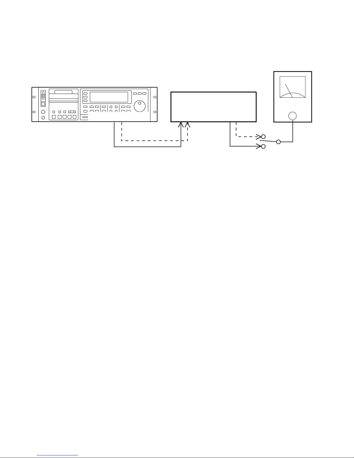
1-1. DA Level Adjustment
D-25 / D-30
5030
BAL IN
AUDIO OUT (XLR)
CH 1
Adjusting points : R192 (for CH 1) on ADDA-2 PCB
R292 (for CH 2) on ADDA-2 PCB
1.
Set up the D-25/D-30 as follows.
Sampling Frequency : 44.1kHz
REF Marker position : -12dB
2.
Connect the Model 5030 input (XLR) to the D-25/D-30 audio output CH 1 and CH 2 and an AC volt meter
to the Model 5030 (RCA) as shown in Fig. 1.
CH 2
(XLR)
Fig. 1
UNBAL OUT
(RCA)
CH 1 CH 2
AC
VOLTMETER
3.
Playback the 1kHz, 0dB section (PROG NO. 1) of SONY test tape TY-7551.
4.
Adjust R192 (CH 1) and R292 (CH 2) on the ADDA-2 PCB so that the AC volt meter reading is +2dBV. By
this adjustment, a 1kHz, +16dBm sine wave should appear at the D-25/D-30 audio output.
4
Page 5
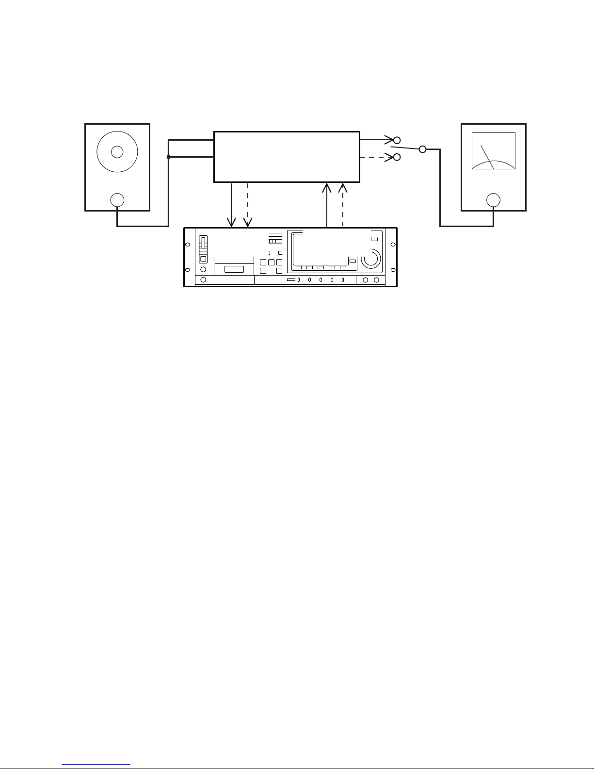
1-2. AD Level Adjustment
D-25/D-30 ADDA-2
CH 1
OSC
CH 2
UNBAL
5030
IN
BAL OUT BAL IN
UNBAL
OUT
CH 1 CH 2
CH 1 CH 2
AUDIO IN
(XLR)
AUDIO OUT
(XLR)
D-25 / D-30
Fig. 2
Adjusting points : R191 (for CH 1) on ADDA-2 PCB
R291 (for CH 2) on ADDA-2 PCB
CH 1
CH 2
AC
VOLTMETER
Set up the D-25/D-30 as follows.
1.
REF Marker position : -12dB
Sampling Frequency : 44.1kHz
A1, A2 INPUT MONITOR Key : ON position
Connect the sine wave oscillator, Model 5030, and AC volt meter with D-25/D-30 as shown in Fig. 2.
2.
Output a 1kHz, +4dBm sine wave signal from the sine wave oscillator. Under this setting, a 1kHz, +4dBm
3.
sine wave signal will be applied to the D-25/D-30 audio input terminal.
Adjust R191 (CH 1) and R291 (CH 2) on the ADDA-2 PCB so that the AC volt meter reading is -10dBV.
4.
5
Page 6

D-25/D-30 ADDA-2
3. PARTS LIST
Ref. No. Part No. Description
U001 8236540301 ST , AN, REGULATOR, NJM78M05D
U002 8236561004 ST, DG, 74HCU04
U003-006 8236570101 ST, DG, DRIVER, DTC114EK
U007-013 8236570401 ST, DG, DRIVER, DTA114EK
U021 8236502700 ST , DA, ADC, AK5340
U022 8236560074 ST, DG, 74HC74
U023 8236560000 ST, DG, 74HC00
U051 8236505300 ST, DA, DAC, AK4320
U052 8236720700 ST , AN, NJM4560M
U081 8236720700 ST , AN, NJM4560M
U101, 201 8236720700 ST, AN, NJM4560M
U102, 202 8236505011 ST, AN, OP AMP, NJM2115M(TEI)
U141, 241 8236720700 ST, AN, NJM4560M
Ref.No. PartNo. Description
Q101, 201 8234143403 TR, VT, NPN, 2SC2878-A/B
Q102, 202 8234143403 TR, VT, NPN, 2SC2878-A/B
Q103, 203 8234143403 TR, VT, NPN, 2SC2878-A/B
Q104, 204 8234143403 TR, VT, NPN, 2SC2878-A/B
Q141, 241 8234143403 TR, VT, NPN, 2SC2878-A/B
Q142, 242 8234143403 TR, VT, NPN,. 2SC2878-A/B
Q143, 243 8234143403 TR, VT, NPN, 2SC2878-A/B
Q144, 244 8234143403 TR, VT, NPN, 2SC2878-A/B
Q181, 281 8234143403 TR, VT, NPN, 2SC2878-A/B
Ref.No. PartNo. Description
D001, 002 8234502800 D, ST, DAN202K
D101, 201 8234502800 D, ST, DAN202K
D102, 202 8234502800 D, ST, DAN202K
D103, 203 8234502800 D, ST, DAN202K
D104, 204 8234502800 D, ST, DAN202K
D141, 241 8234502800 D, ST, DAN202K
D142, 242 8234502800 D, ST, DAN202K
D143, 243 8234502800 D, ST, DAN202K
D144, 244 8234502800 D, ST, DAN202K
D181, 281 8234502800 D, ST, DAN202K
Ref. No. Part No. Description
R001 8230112101 H, METAL, 1W, 100, 5%, F1
R002-005 8230500103 ST, CARBON, 1/10W, 10K, 5%
R006-013 8230500104 ST, CARBON, 1/10W, 100K, 5%
R021 8230500562 ST, CARBON, 1/10W, 5.6K, 5%
R022 8230500112 ST, CARBON, 1/10W, 1.1K, 5%
R023 8230500100 ST, CARBON, 1/10W, 10, 5%
8274121000 PCB Assy , ADDA-2, D-25/D-30
ICs
TRANSISTORs
DIODEs
RESISTORs
RESISTORs
Ref. No. Part No. Description
R101, 201 8230500123 ST, CARBON, 1/10W, 12K, 5%
R102, 202 8230500473 ST, CARBON, 1/10W, 47K, 5%
R103, 203 8230500103 ST, CARBON, 1/10W, 10K, 5%
R104, 204 8230500103 ST, CARBON, 1/10W, 10K, 5%
R105, 205 8230500183 ST, CARBON, 1/10W, 18K, 5%
R106, 206 8230500332 ST, CARBON, 1/10W, 3.3K, 5%
R107, 207 8230500392 ST, CARBON, 1/10W, 3.9K, 5%
R108, 208 8230500562 ST, CARBON, 1/10W, 5.6K, 5%
R109, 209 8230500222 ST, CARBON, 1/10W, 2.2K, 5%
R110, 210 8230500222 ST, CARBON, 1/10W, 2.2K, 5%
R111, 211 8230500222 ST, CARBON, 1/10W, 2.2K, 5%
R112, 212 8230500103 ST, CARBON, 1/10W, 10K, 5%
R113, 213 8230500103 ST, CARBON, 1/10W, 10K, 5%
R114, 214 8230500272 ST, CARBON, 1/10W, 2.7K, 5%
R115, 215 8230500222 ST, CARBON, 1/10W, 2.2K, 5%
R116, 216 8230500122 ST, CARBON, 1/10W, 1.2K, 5%
R117, 217 8230500473 ST, CARBON, 1/10W, 47K, 5%
R118, 218 8230500105 ST, CARBON, 1/10W, 1M, 5%
R119, 219 8230500562 ST, CARBON, 1/10W, 5.6K, 5%
R120, 220 8230500562 ST, CARBON, 1/10W, 5.6K, 5%
R121, 221 8230500103 ST, CARBON, 1/10W, 10K, 5%
R122, 222 8230500472 ST, CARBON, 1/10W, 4.7K, 5%
R123, 223 8230500103 ST, CARBON, 1/10W, 10K, 5%
R124, 224 8230500103 ST, CARBON, 1/10W, 10K, 5%
R125, 225 8230500331 ST, CARBON, 1/10W, 330, 5%
R126, 226 8230500331 ST, CARBON, 1/10W, 330, 5%
R127, 227 8230500102 ST, CARBON, 1/10W, 1K, 5%
R128, 228 8230500102 ST, CARBON, 1/10W, 1K, 5%
R141, 241 8230500103 ST, CARBON, 1/10W, 10K, 5%
R142, 242 8230500272 ST, CARBON, 1/10W, 2.7K, 5%
R143, 243 8230500103 ST, CARBON, 1/10W, 10K, 5%
R144, 244 8230500562 ST, CARBON, 1/10W, 5.6K, 5%
R145, 245 8230500222 ST, CARBON, 1/10W, 2.2K, 5%
R146, 246 8230500122 ST, CARBON, 1/10W, 1.2K, 5%
R147, 247 8230500473 ST, CARBON, 1/10W, 47K, 5%
R148, 248 8230500105 ST, CARBON, 1/10W, 1M, 5%
R149, 249 8230500562 ST, CARBON, 1/10W, 5.6K, 5%
R150, 250 8230500103 ST, CARBON, 1/10W, 10K, 5%
R151, 251 8230500103 ST, CARBON, 1/10W, 10K, 5%
R152, 252 8230500472 ST, CARBON, 1/10W, 4.7K, 5%
R153, 253 8230500182 ST, CARBON, 1/10W, 1.8K, 5%
R154, 254 8230500103 ST, CARBON, 1/10W, 10K, 5%
R155, 255 8230500101 ST, CARBON, 1/10W, 100, 5%
R156, 256 8230500103 ST, CARBON, 1/10W, 10K, 5%
R157, 257 8230500183 ST, CARBON, 1/10W, 18K, 5%
R158, 258 8230500332 ST, CARBON, 1/10W, 3.3K, 5%
R159, 259 8230500392 ST, CARBON, 1/10W, 3.9K, 5%
6
Page 7

D-25/D-30 ADDA-2
RESISTORs
Ref. No. Part No. Description
R160, 260 8230500562 ST, CARBON, 1/10W, 5.6K, 5%
R161, 261 8230500222 ST, CARBON, 1/10W, 2.2K, 5%
R162, 262 8230500222 ST, CARBON, 1/10W, 2.2K, 5%
R163, 263 8230500222 ST, CARBON, 1/10W, 2.2K, 5%
R181, 281 8230500331 ST, CARBON, 1/10W, 330, 5%
R182, 282 8230500103 ST, CARBON, 1/10W, 10K, 5%
R183, 283 8230500103 ST, CARBON, 1/10W, 10K, 5%
R184, 284 8230503471 ST, CARBON, 1/2W, 470, 5%
R185, 285 8230500101 ST, CARBON, 1/10W, 100, 5%
R186, 286 8230500104 ST, CARBON, 1/10W, 100K, 5%
R191, 291 8231014472 R-TRIM, H, CARBON, 4.7K, 637A
R192, 292 8231014472 R-TRIM, H, CARBON, 4.7K, 637A
CAPACITORs
ALU = Electrolytic
CER = Ceramic type
Ref. No. Part No. Description
C001, 002 8232145106 VT, ALU, 35V, 10µF, 20%
C003, 004 8232145106 VT, ALU, 35V, 10µF, 20%
C005 8232144476 VT, ALU, 25V, 47µF, 20%
C006 8233504103 ST, CER, 25V, 0.01µF, 10%
C007 8232142107 VT, ALU, 10V, 100µF, 20%
C008 8232144476 VT, ALU, 25V, 47µF, 20%
C009 8233502104 ST, CER, 50V, 0.1µF, +80
C010 8233502104 ST, CER, 50V, 0.1µF, +80
C011 8232144476 VT, ALU, 25V, 47µF, 20%
C012 8233504103 ST, CER, 25V, 0.01µF, 10%
C021 8232143106 VT, ALU, 16V, 10µF, 20%
C022, 023 8233504103 ST, CER, 25V, 0.01µF, 10%
C024~027 8233504103 ST, CER, 25V, 0.01 µF, 10%
C028 8232143106 VT, ALU, 16V, 10µF, 20%
C029 8232146475 VT, ALU, 50V, 4.7µF, 20%
C030, 031 8233504103 ST, CER, 25V, 0.01µF, 10%
C032 8232143106 VT, ALU, 16V, 10µF, 20%
C033 8233504103 ST, CER, 25V, 0.01µF, 10%
C034 8233504103 ST, CER, 25V, 0.01µF, 10%
C035 8233504103 ST, CER, 25V, 0.01µF, 10%
C036 8233502104 ST, CER, 50V, 0.1µF, +80
C037 8232143106 VT, ALU, 16V, 10µF, 20%
C038 8233504103 ST, CER, 25V, 0.01µF, 10%
C051 8233504103 ST, CER, 25V, 0.01µF, 10%
C052 8233504103 ST, CER, 25V, 0.01µF, 10%
C053 8232143106 VT, ALU, 16V, 10µF, 20%
C054 8233502104 ST, CER, 50V, 0.1µF, +80
C055 8232143106 VT, ALU, 16V, 10µF, 20%
C056 8233502104 ST, CER, 50V, 0.1µF, +80
C057 8232143476 VT, ALU, 16V, 47µF, 20%
C058 8233502104 ST, CER, 50V, 0.1µF, +80
C060~063 8233504103 ST, CER, 25V, 0.01 µF, 10%
C064, 065 8233504103 ST, CER, 25V, 0.01µF, 10%
C081, 082 8233504103 ST, CER, 25V, 0.01µF, 10%
CAPACITORs
Ref. No. Part No. Description
C101, 201 8232145106 VT, ALU, 35V, 10µF, 20%
C103, 203 8233500100 ST, CER, 50V, 10PF, 5%
C104, 204 8232144476 VT, ALU, 25V, 47µF, 20%
C105, 205 8232145106 VT, ALU, 35V, 10µF, 20%
C106, 206 8233504472 ST, CER, 25V, .0047µF, 10%
C107, 207 8233504822 ST, CER, 25V, .0082µF, 10%
C109, 209 8233500100 ST, CER, 50V, 10PF, 5%
C110, 210 8232144476 VT, ALU, 25V, 47µF, 20%
C111, 211 8233504103 ST, CER, 25V, 0.01µF, 10%
C112, 212 8233504103 ST, CER, 25V, 0.01µF, 10%
C113, 213 8232143476 VT, ALU, 16V, 47µF, 20%
C114, 215 8233500101 ST, CER, 50V, 100PF, 5%
C117, 217 8233500220 ST, CER, 50V, 22PF, 5%
C118, 218 8233504103 ST, CER, 25V, 0.01µF, 10%
C119, 219 8232143106 VT, ALU, 16V, 10µF, 20%
C120, 220 8232143106 VT, ALU, 16V, 10µF, 20%
C121, 221 8233500152 ST, CER, 50V, .0015µF, 5%
C122, 222 8232143106 VT, ALU, 16V, 10µF, 20%
C123, 223 8233504103 ST, CER, 25V, 0.01µF, 10%
C141, 241 8232143476 VT, ALU, 16V, 47µF, 20%
C143, 243 8233500681 ST, CER, 50V, 680PF, 5%
C144, 244 8233504472 ST, CER, 25V, .0047µF, 10%
C145, 245 8233504822 ST, CER, 25V, .0082µF, 10%
C147, 247 8233500100 ST, CER, 50V, 10PF, 5%
C148, 248 8233504103 ST, CER, 25V, 0.01µF, 10%
C149, 249 8233504103 ST, CER, 25V, 0.01µF, 10%
C150, 250 8232143476 VT, ALU, 16V, 47µF, 20%
C152, 252 8233500100 ST, CER, 50V, 10PF, 5%
C153, 253 8232144476 VT, ALU, 25V, 47µF, 20%
C182, 282 8233500100 ST, CER, 50V, 10PF, 5%
C183, 283 8232145106 VT, ALU, 35V, 10µF, 20%
MISCELLANEOUS
Ref. No. Part No. Description
B101 8251515000 Plain PCB, ADDA-2, D-25/D-30
J001 8245053029 CONN, PI, JACK, 8263, 9P, RED
J002 8245272025 CONN, PI, JACK, FPC, 25P
J003 8245171113 CONN, PI, JACK, 8283, 13P, WHT
J004 8245171113 CONN, PI, JACK, 8283, 13P, WHT
J005 8245171106 CONN, PI, JACK, 8283, 6P, WHT
J006 8245171107 CONN, PI, JACK, 8283, 7P, WHT
L001 8242135001 COIL, 50µH, SKP-2-30
L021 8242196223 COIL, PVT, 22µH, 5%, LF5.0S
L051 8242196223 COIL, PVT, 22µH, 5%, LF5.0S
Y1601 8207006102 Spacer, MPS-04
7
Page 8

D-25/D-30 ADDA-2
8
L1
C201
Q202
Q102
C204
C104
R212
R291
R191
C203
R208
R207
R206
R205
R217
R216
C207
C206
R208
R207
R206
R205
6
J5
1
Q103
Q281
Q142
C153
C253
Q143
Q243
Q242
Q244
R260
R259
R258
R257
R160
R159
R158
R157
U81
Q181
R284
C181
C281
R254
R255
R250
C247
C246
C146
R247
R246
R244
C244
C245
C248
C249
C243
R242
U52
C242
C142
C143
C241
C57
L51
C55
C141
C250
R252
R152
C150
U241
R292
Q241
C56
C54
C53
U51
R142
Q141
R192
U141
C282
C282
R281
R181
R184
C283
C183
Q201
Q101
R285
R185
Q144
C101
EEE
BBB
E
E
E
E
E
E
E
E
E
B
B
B
B
B
B
B
BBB
E
E
E
BBB
U201
U202
U102
U21
U2 U22
U9
R9
D204
D104
D101
D102
D103
D201
D202
D203
D281
D181
D144
D143
D142
D244
D243
D242
D241
D141
R27
R10
R11
C24
R12
C25
R13
C26
R283
R145
R211
R115
R110
R209
R215
R6
R8
R7
C83
R162
R161
C63
C62
C61
C60
U10
U11
U12
U13
U3
U4
U7
U8
U5
U6
D2
D1
U23
L21
1
15
888
111
C210
C110
U101
C211
C212
R223
R225
C30
R23 C36
C38
C37
J2
25 1
C29
R226
R126
R125
C28
R123
C222
C213
C122C113
C205
C105
R201
C102
R101
U1
R1
3
1
C8
C5
9
13
13
1
1
17
1
J1
J3
J4
ANALOG I/O CH1
ANALOG I/O CH2
J6
POWER
PHONES
C6
C7
C1 C2 C3 C4
C11
C202
C215
R221
R222
C115
R122
R224
C217
C221C121
C216
R124
C117
C116
R230
R229
C219
C220
R130
R129
C119
C120
C32
C21
R109R163
R262
R111
C12
C22
R3
R2R4
R5
R21
C214
C114
C208
R219
C209
R220
R119
C109
R120
Q204
R203
BE
Q104
BE
R103
1
1
1
1
1
1
1
13
1
5
5
5
5
5
5
1
5
5
C103
R112
R117
R116
C107
C106
C108
R189
R263
R261
R245
R210
R291 : AD LEVEL CH2
R191 : AD LEVEL CH1
R292 : DA LEVEL CH2
R192 : DA LEVEL CH1
R154
R155
R250
C247
R247
R246
R244
C144
C145
PARTS SIDE VIEW
4. PATTERN DRAWING
Page 9

9
D-25/D-30 ADDA-2
1
J2
25
C37
L21
C29
C28
C119
C120
C219
C222
C213
C220
C21
C35
C34
R227
R218
Q204
B
E
C210
Q201
EEE
BBB
1
9
1
1
1
7
6
Q202
Q203
R214
R213
R202
C204
R204
C205
C122
C113
R291
C201
Q101
E
E
E
E
E
E
B
BBB
B
B
Q102
Q103
Q242
Q243
Q244
BBB
Q142
Q143
Q144
C112
C111
R114
R113
R102
C104
J5
J5
J6
J3
J4
R286
R282
C82
R182
C81
R186
13
13
C11
C7
C1 C2 C3 C4
C5
C10
C9
C8
R104
C105
C252
R251
R151
C149
R249
R248
R149
R148
C251
C152
C151
C66
C148
R256
E
E
E
R156
R253
R153
R191
C253
C153
BE
B
E
Q181
Q281
C283
C183
R292
C250
E
B
Q241
C150
E
B
Q141
R192
C201
L1
R1
R118
Q104
B
E
C110
R228C39
C223
C218
R127
R128
C123
C118
C31
C32
C59
C51
C53
C52
C58
R241
C64
C65
R243
R141
R143
C55
CL51
C57
C241
C141
R22
C33
FOIL SIDE VIEW
Page 10

D-25/D-30 ADDA-2
10
A+24
AGND
8283-13P
ANALOG I/O 1
AGNDO
AGNDO1
A-24
A-18
A+18
13
12
11
10
9
8
7
6
5
4
3
2
1
AGNDO
MOUT1
AGNDI1
AIN1
AGNDO1
AOUT1
LINEMUTE
A-18
AGND
A+18
A-24
AGNDO
A+24
J3
A+24
AGND
8283-13P
ANALOG I/O 2
8283-6P
INPUT VOLUME
8283-7P
PHONES AMP
8263-9P(RED)
AGNDO
AGNDO2
A-24
A-18
A+18
13
12
11
10
9
8
7
6
5
4
3
2
1
AGNDO
MOUT2
AGNDI2
AIN2
AGNDO2
AOUT2
LINEMUTE
A-18
AGND
A+18
A-24
AGNDO
A+24
J4
7
6
5
4
3
2
1
AOUT2
AGNDO
AOUT1
PHONESMUTE
A-24
AGNDO
A+24
J5
6
5
4
3
2
1
VLIN2
AIN2
AGNDI2
VLIN1
AIN1
AGNDI1
J5
A+24
A-24
A+24
A+18
AGND
A-18
A-24
A+5
DGND1
VCCD+5
GNDDGND
AGNDO
C1
10/16
C3
10/16
C4
10/16
R1
100(1W)
L1
50µH
C5
47/25
C8
47/25C90.1
C10
0.1
C11
47/25
C12
0.01
C6
0.01
C7
100/10
U1
NJM78M05FA
3
INGOUT
1
2
C2
10/16
AGNDO
AOUT1
AGNDO1
AOUT2
AGNDO2
A+18
A-18
A+18
A-18
A+5
DGND1
A+5
DGND1
MSCK
DA
DAAD
BCK
LRCK
L-20
L-18
L-12
/RST_ADDA
DA_DATA
EMPHA
MSCK
BCK
LRCK
L-18
L-12
L-10
RST_ADDA
AD_MUTE
AD_DATA
EMPHA
VLIN1
AGNDI1
AGNDI1
VLIN2
AGNDI2
AGNDI2
AD
A+18
A-18
A+18
A-18
A+5
DGND1
A+5
DGND1
D+5
DGND
D+5
DGND
AOUT1
AOUT2
MONIMUTE
A+18
A-18
A+18
A-18
MOUT1
MONITOR
AGNDO1
MOUT2
AGNDO2
MONITOR
9
8
7
6
5
4
3
2
1
J1
MUTDRV
DGND
D+5
A-18
AGND
A+18
A-24
AGNDO
A+24
8370-25P
CN-BOARD
13
12
11
10
9
8
7
6
5
4
3
2
1
26
25
24
23
22
21
20
19
18
17
16
15
14
LVL1
LVL2
LVL3
LVL4
/EMPHA
/MONIMUTE
/LINEMUTE
AD_MUTE
RST_ADDA
LRCK
BCK
DA_DATA
AD_DATA
/RST
DGND
DGND
1
U2A U2B
LINEMUTE
MONIMUTE
PHONESMUTE
BCK_ADDA
/RST_ADDA
RST_ADDA
LRCK_ADDA
U2C
74HCU04
74HCU04
74HCU04
74HCU04
74HCU04
74HCU04
U3
DTC114EK
23123
1
2312
DGND
DGND
A+5
3
1
23
1
U4
DTC114EK
U7
DTA114EK
23
1
U8
DTA114EK
D1
DAN202K
D2
DAN202K
23
U9
DTA114EK
1
23
U10
DTA114EK
1
23
U11
DTA114EK
1
23
U12
DTA114EK
1
23
U13
DTA114EK
MUTDRV
1
R2
10k
R3
10k
R3
10k
R6 100k
R7 100k
R8 100k
R9 100k
R10 100k
R11 100k
R12 100k
R13 100k
A-18
LINEMUTE
MONIMUTE
PHONESMUTE
EMPHA
LVL4
LVL3
LVL2
LVL1
R4
10k
U5
DTC114EKU6DTC114EK
U2D
U2E
U2F
23 4
5698
11 10
13 12
MSCK
128FS
FOSC
J2
5. CIRCUIT DIAGRAMS
ADDA2, ROOT
Page 11

11
D-25/D-30 ADDA-2
AGNDI1
AGNDI1
VLIN1
R101
12k
R102
47k
R104
10k
R105
18k
Q101
2SC2878
R109 2.2k D101 DAN202K
R110 2.2k D102 DAN202K
R111 2.2k D103 DAN202K
Q102
2SC2878
Q103
2SC2878
R106
3.3k
R107
3.9k
R108
5.6k
R112
10k
R191
4.7k(B)
ADLVL1
R113
10k
C27
0.01
R114
NON
R115
2.2k
Q104
2SC2878
D104
DAN202K
C105
JUMPER
C102
NON
C103 10p
R103 10k
U101B
NJM4560M
5
6
7
C101
10/35
C104
47/25
L-18
L-18
L-18
EMPHA
R118
1M
R120
5.6k
R128
1k
C122
10/16
C123
0.01
R127
1k
R117
47k
R116
1.2k
C106
0.0047
C107
0.0082
U101A
NJM4560M
U102A
NJM2115M
U102B
NJM2115M
328
4
1
AGNDI1
C108
NON
C114
NON
C116
NON
R129
NON
R130
NON
R125
330
R126
330
C121
1500p
R123
10k
C117
22p
C119
10/16
C120
10/16
R124
10k
C111
0.01
C113
47/16
R121
10k
A+5
C118
0.01
C115
100p
R122
4.7k
AGNDI1
ADIN1+
ADIN1-
C112
0.01
C109 10p
R119 5.6k
A+18
A-18
A+5
C110
47/25
328
4
1
6
5
7
AGNDI2
AGNDI2
VLIN2
R201
12k
R202
47k
R204
10k
R205
18k
Q201
2SC2878
R209 2.2k D201 DAN202K
R210 2.2k D202 DAN202K
R211 2.2k D203 DAN202K
Q202
2SC2878
Q203
2SC2878
R206
3.3k
R207
3.9k
R208
5.6k
R212
10k
1
3
2
1
3
2
R291
4.7k(B)
ADLVL1
R213
10k
R214
NON
R215
2.2k
Q204
2SC2878
D204
DAN202K
C205
JUMPER
C202
NON
C203 10p
R203 10k
U201B
NJM4560M
5
6
7
C201
10/35
C24 0.01
C25 0.01
C26 0.01
AGNDI1
AGNDI1AGNDI3
AGNDI3
AGNDI3
AGNDI3 AGNDI3
DGND1
AGNDI2
C204
47/25
R218
1M
R220
5.6k
R228
1k
C222
10/16
C223
0.01
R227
1k
R217
47k
R216
1.2k
C206
0.0047
C207
0.0082
U201A
NJM4560M
U202A
NJM2115M
U202B
NJM2115M
328
4
1
C208
NON
C214
NON
C216
NON
R229
NON
R230
NON
R225
330
R226
330
C221
1500p
R223
10k
C217
22p
C219
10/16
C220
10/16
R224
10k
C211
0.01
C213
47/16
R221
10k
A+5
D+5 D+5
D
S
R
11
12
13
11
8
12
10
9
10
13
8
9
CQQ
C218
0.01
U22B
74HC74
U23C
74HC00
U23D
74HC00
C215
100p
R222
4.7k
AGNDI2
ADIN2+
ADIN2-
C212
0.01
C209 10p
R219 5.6k
A+18
A-18
A+5
C210
47/25
328
4
1
6
5
7
6
5
4
3
2
1
U23A
74HC00
U23B
74HC00
AD DATA
D
S
R
CQQ
U22A
74HC74
AD_MUTE
3
2
4
1
6
5
A+5
A+5
DGND1
DGND1
D+5
VCC
GND
D+5
DGND
DGND
A+18
A+18
A-18
A-18
C39
NON
C28
10/16
R21
5.6k
R22
1.1k
C29
4.7/50
C32
10/16
C33
0.01
C30
0.01
C31
0.01
C21
10/16
C22
0.01
C23
0.01
L21
22µH
AINL+
AINLVREFIN
VA+
VGND
NC
NC
TST1
SEL18
PD
TST2
CMODE
SMODE
L/R
AINR+
AINRVREF
NC
VDB+
NC
TST4
TST3
CLK
DGND
VDP+
FSYNC
SDATA
SCLK
1
2
3
4
5
6
7
8
9
10
11
12
13
14
28
27
26
25
24
23
22
21
20
19
18
17
16
15
RST_ADDA
LRCK
ADIN1+
ADIN1-
U21
AK5340
ADIN1+
ADIN1-
C35
0.01
C34
0.01
C36
0.01
R23
10
C38
0.01
C37
10/16
DGND1
DGND1
AGNDI3
AGNDI3
MSCK
BCK
ADDA2, AD
Page 12

D-25/D-30 ADDA-2
12
CKS
DVDD
DVSS
XTO
XTI
PD
BICK
SDATA
LRCK
SMUTE
HOLD
DEMO
ZMUTE
DZF
VREF
AVSS
AVDD
VCOM
AOUTL
AOUTR
VCNT
DIF1
DIF0
DEM1
1
2
3
4
5
6
7
8
9
10
11
12
24
23
22
21
20
19
18
17
16
15
14
13
U51
AK4320
C54
0.1
C52
0.01
C53
10/16
C51
0.01
AGNDO3
A+5
DGND1
DGND1
DAOUT2
DAOUT1
AGNDO3
L21
22µH
MSCK
/RST_ADDA
BCK
DA_DATA
LRCK
C56
0.1
C55
10/16
C58
0.1
C59
NON
C57
47/16
R242
2.7k
R244
5.6k
R246
1.2k
R247
47k
C244
0.0047
C245
0.0082
R248
1M
C243
680p
C242
NON
R241
10k
R243
10k
U52B
NJM4560M
5
6
7
C241
47/16
R250
10k
C247
10p
C248
0.01
C61
0.01
C62
0.01
C63
0.01
C250
47/16
R252
4.7k
R253
1.8k
C249
0.01
C246
NON
R251
10k
A-18
A+18
R249
5.6k
U241A
NJM4560M
328
4
1
R245
2.2k
Q241
2SC2878
D241
DAN202K
R256
10k
R262
2.2k
R257
18k
Q242
2SC2878
Q243
2SC2878
Q244
2SC2878
R258
3.3k
R254
10k
R255
100
C252
10p
R259
3.9k
R260
5.6k
C251
NON
U241B
NJM4560M
5
6
7
C253
47/25
1
3
2
R292
4.7k(B)
DALVL1
AGNDO2
AGNDO2
D243 DAN202K
R263
2.2k
D244 DAN202K
R261
2.2k
D242 DAN202K
AOUT2
R142
2.7k
R144
5.6k
R146
1.2k
R147
47k
C144
0.0047
C145
0.0082
R148
1M
C143
680p
C64
0.01
C142
NON
R141
10k
R143
10k
U52A
NJM4560M
A-18
AGNDO3
AGNDO1
A+18
328
4
1
C141
47/16
R150
10k
C147
10p
C148
0.01
C150
47/16
R152
4.7k
R153
1.8k
C149
0.01
C146
NON
R151
10k
A-18
A+18
R149
5.6k
U141A
NJM4560M
328
4
1
R145
2.2k
Q141
2SC2878
D141
DAN202K
R156
10k
R162
2.2k
R157
18k
Q142
2SC2878
Q143
2SC2878
Q144
2SC2878
R158
3.3k
R154
10k
R155
100
C152
10p
R159
3.9k
R160
5.6k
C151
NON
U141B
NJM4560M
5
6
7
C153
47/25
1
3
2
R192
4.7k(B)
DALVL1
AGNDO1
AGNDO1
AGNDO1
D143 DAN202K
R163
2.2k
D144 DAN202K
R161
2.2k
D142 DAN202K
AOUT1
C65
0.01
C60
0.01
EMPHA
L-12
L-18
L-20
AGNDO1AGNDO3 AGNDO2
A+5
A+5
DGND1
DGND1
A+18
A+18
A-18
A-18
C66
NON
ADDA2, DA
Page 13

13
D-25/D-30 ADDA-2
AOUT1
C182
10p
R181
330
R184
470
R185
100
R186
100k
Q181
2SC2878
C183
10/35
R183
10k
C83
NON
C81
0.01
AGNG01
MONIMUTE
AGND01
C181
NON
R182
10k
1
2
8
3
4
U81A
NJM4560M
C82
0.01
AGNG01
A-18
A+18
D181
DAN202K
MOUT1
AGNG01
AOUT2
C282
10p
R281
330
R284
470
R285
100
R286
100k
Q281
2SC2878
C283
10/35
R283
10k
AGND02
C281
NON
R282
10k
7
6
5
U81B
NJM4560M
D281
DAN202K
MOUT2
AGNG01
AGNG02
A+18
A-18
A-18
A+18
ADDA2, MONITOR
Page 14

D-25/D-30 ADDA-2
FOSTEX CORPORATION 3-2-35 Musashino, Akishima, Tokyo, Japan 196-0021
FOSTEX CORPORATION OF AMERICA 15431 Blackburn Ave., Norwalk, CA 90650, U.S.A.
14
© PRINTED IN JAPAN OCT 1998 8288776000
 Loading...