

Page 1

F 19 SERVICE MANUAL
THIS DOCUMENT IS A PROPERTY
OF INDUSTRIE FORMENTI ITALIA
NO AUTHORIZED MODIFICATIONS
ARE PERMITTED.
CREATED BY E.G.
Page 2

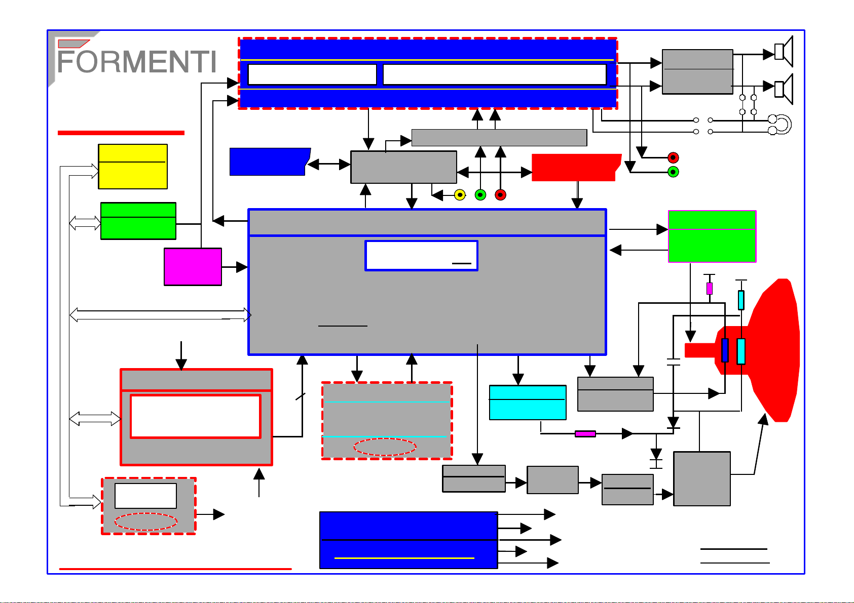
There are two different types of F19 chassis that are equipped with two
From the point of view of the application on the F19 chassis the two type of
Even if the two devices are non interchangeable the two chassis
As the specifications of the two devices are the same and the first version of
different microcontroller.
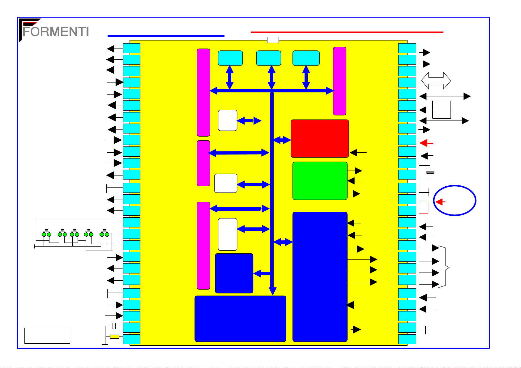
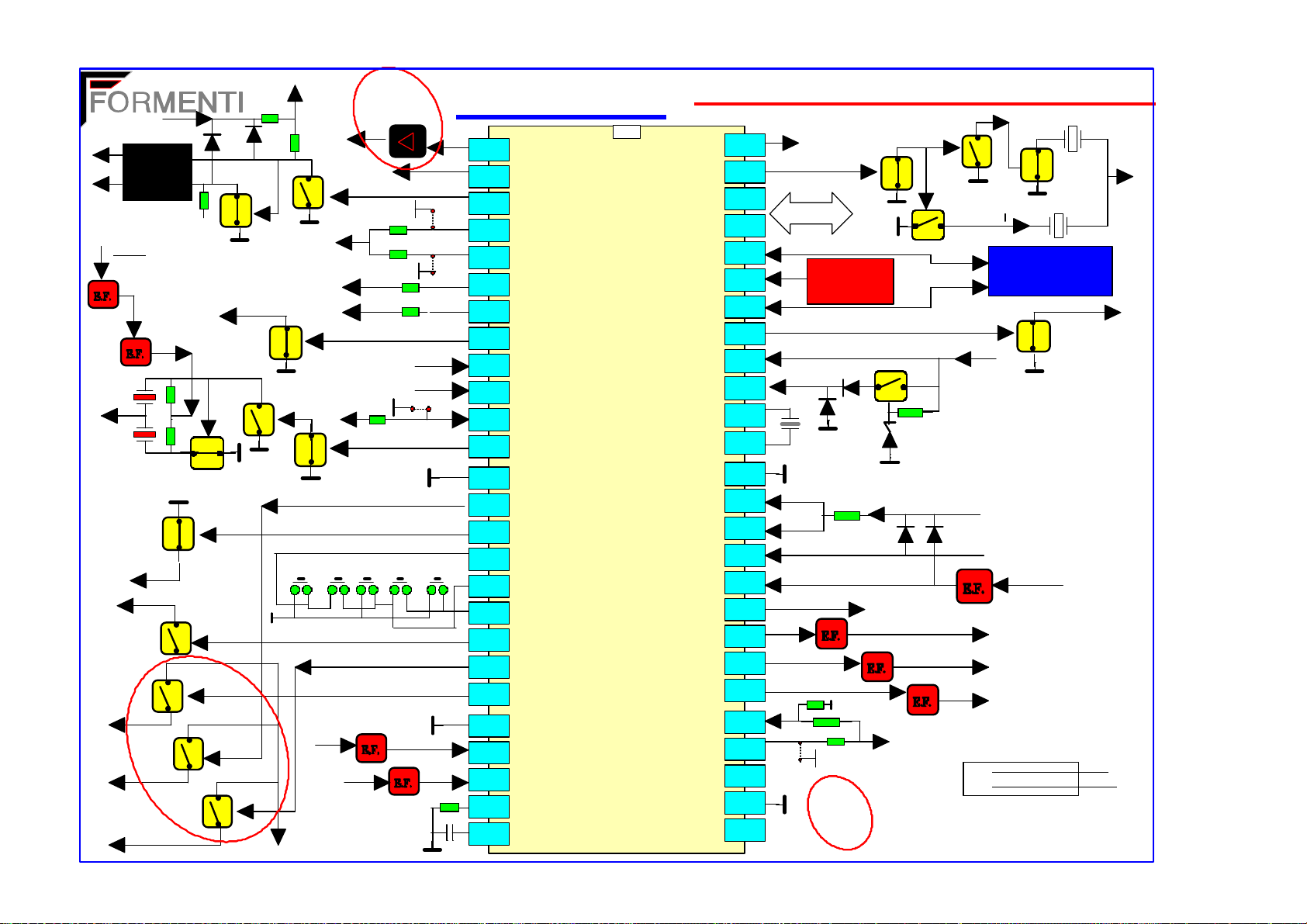
These microcontroller are known as ETT having a code SAA5297A and
PAINTER with a code number SAA5553.
microcontroller are substantially having the same performances, the same pinout , the same firmware but they are not interchangeable as the power supply
are different.
In case of SAA5297A the power supply is 5 V for the SAA5553 is 3.3 V.
can be interchanged as the in/out interface are exactly the same.
the chassis was equipped with the SAA5297A , in this document the
characteristics of it are very much detailed meanwhile there is a very short
description (as an addendum at the end) for the SAA5553.
Page 3

F19 CHASSIS DESCRIPTION
Summary
The F19 is a chassis suitable to drive CRT having both 4 by 3 and 16 to 9 aspect
ratio and dimension from 25" up to 34".
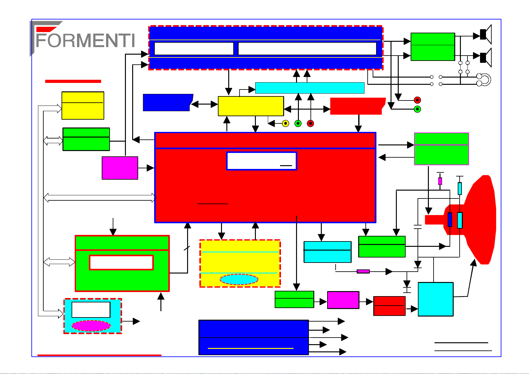
As we can see from the block diagram the chassis is equipped with the most recent
Integrated Circuit like the one chip TV processor TDA884x that does include all the low
level signal processing including Video, Audio, synchronisation process, and chroma
decoder . (see more detail at the "TDA884x FAMILY SPECIFICATION" paragraph), and
the Sound Processor TDA9875A that perform all sound function including digital decoding
of NICAM signals. (see more detail at the " TDA9870A & tda9875A MAIN
CHARACTERISTICS" paragraph).
The above mentioned devices are driven by an Integrated Circuit that does include
the microcontroller function with 64 K ROM and the TELETEXT acquisition and 8 pages
RAM. (SAA5297A)
In the F19 chassis there are, besides the stereo one, two possible module that are
performing "FEATURES" like PIP (picture in picture) and / or CTI (colour transients
improvement) and 4 by 3 to 16 by 9 signal processing. One further module is dedicated to
the so called "Zero Power Stand By"
A 26 Key Remote Control is performing the full control for the end- used but can
also be used in " SERVICE MODE" to control and adjust, without open the back cover of
the TV set all the necessary functions.
With the 5 "LOCAL KEY BOARD" button all the end user function can also be
performed
When the TV set is equipped with a PLL tuner the microcontroller recognise it and
the tuning method became a frequency synthesis system if not it work as a voltage tuning
system (provided all necessary components are mounted)
The TV make use of a multilevel MENU (activated both by the Remote Control and
Local Keyboard) using five selectable languages ( Italian, German, English, France, end
Spanish) with which it is possible to control sequentially all video and sound value, to
adjust several parameter like picture format, sound response, sleep timer etc., and to set
others important parameter like standard, select country for automatic tuning and sort etc.
Here below a list of the characteristics of the TV se
E.G.Data creazione 31/10/99 15.38 1 / 7 f19intro
Page 4

TV SET CHARACTERISTICS (MONO & STEREO )
PICTURE TUBE SIZE :
• 4 : 3 ASPECT RATIO
• 16 : 9 ASPECT RATIO
• STANDARD
• R.F. (ANTENNA) (FOR FREQ. SYNTH.)
• VIDEO (SCART & CINCH)
• COLOUR (MAX. THREE STANDARDS)
• SOUND STANDARD:
∗ MONO
∗ STEREO
TUNING SYSTEM SELECTABLE :
FREQUENCY SYTHETIZER
• TOTAL AVAILABLE CHANNEL NUMBER
• CHANNEL IN ONE RF STANDARD UP TO
• NUMBER OF PROGRAM
• DIRECT PROGRAM & CHANNEL CALL WITH
• PROGRAM & CHANNEL STEP UP AND DOWN
• VOLTAGE SYNTHESISER
• CABLE & HYPERBAND CHANNEL
• SWITCHABLE AFC
• AUTOMATIC SEARCH TUNING
• A S T WITH AUTO SORT
AUDIO SECTION
POWER
• MONO
• STEREO
EXTERNAL CONNECTION
• HEADPHONE
• LOUDSPEAKERS
A / V INPUT / OUTPUT
• FRONT PANEL CINCH
• I FULL SCART (CVBS, STEREO, RBA)
• SCART (CVBS & STEREO IN / OUT)
• SCART A TO SCART B LOOP THROUGH
TXT PANEUROPEAN CHARACTER SET
• LEVEL 1
• LEVEL 1,5 (FASTEXT)
FEATURES
• CTI (COLOUR TRANSIENT IMPROVEMENT)
• 16:9 TO 4:3 VIDEO COMPRESSION
• VERTICAL ZOOM OUT
• MENU DRIVEN SYSTEM
• EASY TO USE REMOTE CONTROL
• REMOTE CONTROL WITH “SERVICE” USE
• PIP
21” / 25” / 28” / 29” / 34”
28 “ / 32”
CCIR ( B / G/ L / L’ / D / K / I )
B / G/ L / L’ / D / K / I / M / N
PAL / SECAM / NTSC
B / G/ L / L’ / D / K / I
AM & FM
A2 OR NICAM
FACTORY OPTION
200
100
100
1, OR 2 OR 3 DIGIT
YES
YES
YES
YES
YES
6 W RMS.
2 x 6 W RMS.
STEREO SET ONLY
INTERNAL L.S. SWITCHED
A / V INPUT
MULTIMEDIA INPUT OUTPUT
VCR, HI.FI, SATELLITE, ETC
FOR PROGRAMS DUBBING
8 PAGES
7 PAGES
OPTION
ONLY FOR 16:9 TV SET
3 LEVEL
NOT ACCESSIBLE TO END USER
OPTION
E.G.Data creazione 31/10/99 15.38 2 / 7 f19intro
Page 5

A U D I O
AUDIO
EEPROM
PCF8582
TUNER
PLL
IIC bus
MICRO
PCA84C841/210
TXT
SAA5281/....
SAA5297A
T.O.P.
PHILIPS
PIP
SIEMENS
THIS MODULE IS PRESENT ONLY FOR STEREO SET
2ND SCART
SAW
FILTER
AUDIO
TDA9875
VIDEO PROCESSOR
AUDIO
VIDEO
&
AUDIO
A/V INA /V OUTA/V IN/OUT
TDA 8362A
S E C A M D.L. CROMA
TDA4661TDA8395
TDA844X
TXT & OSD
R B G
H. DRIVER
BC 639
POWER SUPPLY
TDA 4605 & STH7N80F
PIP (RGB)
FULL SCARTSCART INTER.
RGB
VERTICAL
TDA3654
E.W. GEN.
TDA4950
L.O.T.
BU 508 D
140 V
26 V
15 V
12 V
8 V
RGB
RGB
(OSD)
VIDEO AMPL.
CUT-OFF
TDA1521
TDA5112
V.
RGB
E H T
TRAFO
F16UPF19.DRW
E.G. 2/02/99
110°
H.
EAT
F16
UPDATED
F19
BLOCK DIAGRAM
Page 6
AUDIO STEREO (NICAM) PROCESSOR
2 x 7 W
AUDIO POWER
TDA 9811 (nicam) TDA 9870A (TDA9875A (nicam)
V
I
D
E
I
F 19
EEPROM
PCF8584 /
ST2404CB
TUNER
PLL
IIC bus
IIC bus
LOCAL KEY BOARD
O
A
U
D
I
O
I.
F.
SAW
FILTER
N
T
E
R
VIDEO & AUDIO
C
A
R
2ND SCART
R
I
E
R
IIC BUS ONE CHIP VIDEO PROCESSOR
*IF VIDEO & PLL DEM
*AGC & AFC, MUTE
*AUDIO PLL DEM
*PAL/NTSC (SECAM) DEC.
*B.B CHROMA DELAY LINE
*FULL SCART INTERFACE.
E T T
SAA5297A
IIC bus
F19 BLOCK DIAGRAM
MICROCONTROLLER
& TELETEX 8 PAGES
PIP
OPTION
PIP (RGB)
I.R. INPUT
THIS MODULE IS PRESENT ONLY FOR STEREO SET
AUDIO
A/V IN/OUT
A /V OUT
AUDIO
AUDIO SCART SWITCH HEF4053
VIDEOSCART
SWITCH LA7955
A/V IN
FULL SCART
A/V/ CINCH
(OPTION)
TDA 8843(4)
*H & V SYNC PROCESSIG
*FULL IIC BUS CONTROLL FOR:
*AUTO CUT-OFF
*ALL ANALOGUE FUCTIONS
*GEOMETRY CORRECTION
*FEATURES INTERFACE
E-W-
E-W POWER
BUK474200A
DRIVER
TRAFO
26 V
8 VTDA 4605 & STH7N90F1
4
TXT
& OSD
R B G
U V
FEATURES MODULE
TDA4566 (CTI)
SAA4981 (16:9 TO 4:3)
OPTION
POWER SUPPLY
H DRIVE
H. DRIVER
BC 338
RGB
VERTICAL
TDA8351
E-W DRIVE COIL
BU 508 D
150 V
12 V
5 V
RGB
CUT-OFF
VERTICAL
FEEDBACK
L.O.T.
TDA1521
LINE OUT
(OPTION)
VIDEO AMPL.
TDA5112
RGB
V.
H.
H. DEFL.
& E H T
TRAFO
F19BLDIA.DRW
E.G. 17 / 7 / 99
HEADPHONE
E-W LOAD COIL
CRT
110°
EAT
Page 7
AUDIO STEREO (NICAM) PROCESSOR
2 x 7 W
AUDIO POWER
TDA 9811 (nicam) TDA 9870A (TDA9875A (nicam)
V
I
D
E
I
O
F 19.1
EEPROM
PCF8584 /
ST2404CB
TUNER
PLL
IIC bus
SAW
FILTER
IIC bus
LOCAL KEY BOARD
N
T
A
E
U
D
I
O
I.
F.
VIDEO & AUDIO
R
C
A
2ND SCART
R
R
I
E
R
IIC BUS ONE CHIP VIDEO PROCESSOR
*IF VIDEO & PLL DEM
*AGC & AFC, MUTE
*AUDIO PLL DEM
*PAL/NTSC (SECAM) DEC.
*B.B CHROMA DELAY LINE
*FULL SCART INTERFACE.
E T T
SAA5297A or
SAA5553M3
IIC bus
F19.1 BLOCK DIAGRAM
MICROCONTROLLER
& 8 PAGES TELETEXT
PIP
OPTION
PIP (RGB)
I.R. INPUT
THIS MODULE IS PRESENT ONLY FOR STEREO SET
AUDIO
A/V IN/OUT
A /V OUT
AUDIO
AUDIO SCART SWITCH HEF4053
VIDEOSCART
SWITCH LA7955
A/V IN
FULL SCART
A/V/ CINCH
(OPTION)
TDA 8843(4)
*H & V SYNC PROCESSIG
*FULL IIC BUS CONTROLL FOR:
*AUTO CUT-OFF
*ALL ANALOGUE FUCTIONS
*GEOMETRY CORRECTION
*FEATURES INTERFACE
E-W-
E-W POWER
BUK474200A
DRIVER
TRAFO
26 V
8 VTDA 4605 & STH7N90F1
4
TXT
& OSD
R B G
U V
FEATURES MODULE
TDA4566 (CTI)
SAA4981 (16:9 TO 4:3)
OPTION
POWER SUPPLY
H DRIVE
H. DRIVER
BC 338
RGB
VERTICAL
TDA8351
E-W DRIVE COIL
BU 508 D
150 V
12 V
5 V
RGB
CUT-OFF
VERTICAL
FEEDBACK
L.O.T.
TDA1521
LINE OUT
(OPTION)
VIDEO AMPL.
TDA5112
RGB
V.
H.
H. DEFL.
& E H T
TRAFO
F19BDE&P.DRW
E.G. 22/04/2000
HEADPHONE
E-W LOAD COIL
CRT
110°
EAT
Page 8

F19 TUNINGF19 TUNING
&&
TELETEXTTELETEXT
Page 9

SAA529XA FAMILY MAIN CHARACTERISTICS
FEATURES
General
• Single chip microcontroller with integrated teletext decoder
• Single +5 V power supply
• Single crystal oscillator for teletext decoder, display and microcontroller
• Teletext function can be powered-down independent of microcontroller function for
reduced power consumption in standby
• Pin compatibility throughout family.
Microcontroller
• 80C51 microcontroller core
• 16/32/64 kbyte mask programmed ROM
• 256/768/1280 bytes of microcontroller RAM
• Eight 6-bit Pulse Width Modulator (PWM) outputs for control of TV analog signals
• One 14-bit PWM for Voltage Synthesis Tuner control
• Four 8-bit Analog-to-Digital converters
• 2 high current open-drain outputs for directly driving LEDs etc.
• I 2 C-bus interface
• External ROM and RAM capability on QFP80 package version.
Teletext acquisition
• 1 page and 10 page Teletext version
• Acquisition of 525-line and 625-line World System Teletext, with automatic selection
• Acquisition and decoding of VPS data (PDC system A)
• Page clearing in under 64 s (1 TV line)
• Separate storage of extension packets (SAA5296/7, SAA5296/7A and SAA5496/7)
• Inventory of transmitted Teletext pages stored in the Transmitted Page Table (TPT)
end Subtitle Page Table (SPT) (SAA5296/7, SAA5296/7A and SAA5496/7)
• Automatic detection of FASTEXT transmission
E.G.Data creazione 01/11/99 17.27 8 / 30 F19MANU.doc
Page 10

TO CURRENT INTEGRATOR
VOLTAGE SINTESYS ONLY
FRANCE STD. SWITCH
CTI DETECTOR
16 : 9 DETECTOR
SCART1 / SCART2 SWITCH
SCART 1 / TV
TO SCART 2 SWITCH
FRONT CINCH / SCART1
SWITCH
SCART 1 INPUT DETECTOR
SCART 2 INPUT DETECTOR
HEAD PHONES DETECTOR
STANDARD SWITCH
UHF SUPPLY
(VOLTAGE SINTESYS ONLY)
TV / AV SWITCH
MENU V - V + P - P +
LOCAL KEY BOARD
TV ON / OFF SWITCH
TUNER SUPPLY (V.S. ONLY)
TUNER SUPPLY(V.S. ONLY)
CVBS FROM ANTENNA
CVBS FROM SCART
SAA5297A.DRW
E.G . 17 / 10 / 99
DATA
SLICER
REF.PIN
TO X13
SAA5297A
1
V TUN.
2
DSC
3
SWT. L/L'
4
CTI STS.
5
16:9 STS
6
SWT. S1/S2
7
COPY SWT.
8
SWT. CI/S1
9
AV1 STS.
10
AV2 STS.
11
H.P. STS.
12
SYSTEM
13
VSS M+T
14
UHF
15
TV / AV
16
P0.3
17
P0.4
18
P0.5
19
ON / OFF
20
VHF H
21
VHF L
22
VSSA
23
CVBS0
24
CVBS1
25
BLACK
26
IREF
P
O
R
T
2
P
O
R
T
3
P
O
R
T
0
T X T DATA
SLICER &
ACQUISITION
MICRO & TXT Block Diagram
ROM RAM TIMER
A/ D
8051
CORE
B
U
PWM
S
TXT
INT
PAGE
RAM
OSCILLATOR
DISPLAY
DISPLAY
P
O
R
T
1
TIMING
SWT 16:9
OSC. SWT.
MSDA
MSCL
SDA 1
INTO
SCL 1
AM/FM
VDDM
RESET
OSCOUT
OSCIN
OSCGND
VDDT
VDDA
VSYNC
HSYNC
BLK
RGBREF
PIP STS
INT. TEST
FRAME
R
G
B
52
51
50
49
48
47
46
45
44
43
42
41
40
39
38
37
36
35
34
33
32
31
30
29
28
27
TO CHANGE
ASPECT RATIO
TO SWITCH S.C.
FROM 4.43
TO 3.58 MHz
MAIN
IIC BUS
IIC BUS
FOR
I.R.
EEPROM
SOUND STANDARD
SWITCH
5 V from ST-BY
FROM
RESESET CIRCUIT
QZ100
12 MHz
5 V
VERTICAL
FLYBACK
HORIZONTAL
FLYBACK PULSE
TO
TDA884X
RGB REFERENCE
VOLTAGE
2,5 V
PIP DETECTOR
NOT CONNECTED
NOT CONNECTED
Page 11
TO CURRENT INTEGRATOR
VOLTAGE SINTESYS ONLY
TO X13
FRANCE STD. SWITCH
CTI DETECTOR
16 : 9 DETECTOR
SCART1 / SCART2 SWITCH
SCART 1 / TV
TO SCART 2 SWITCH
FRONT CINCH / SCART1
SWITCH
SCART 1 INPUT DETECTOR
SCART 2 INPUT DETECTOR
HEAD PHONES DETECTOR
STANDARD SWITCH
UHF SUPPLY
(VOLTAGE SINTESYS ONLY)
TV / AV SWITCH
MENU V - V + P - P +
LOCAL KEY BOARD
TV ON / OFF SWITCH
TUNER SUPPLY (V.S. ONLY)
TUNER SUPPLY(V.S. ONLY)
CVBS FROM ANTENNA
CVBS FROM SCART
DATA
SAA5553.DRW
E.G 22/ 04 / 2000
SLICER
REF.PIN
SAA5553M3
1
V TUN.
DSC
2
3
SWT. L/L'
CTI STS.
4
5
16:9 STS
SWT. S1/S2
6
7
COPY SWT.
SWT. CI/S1
8
9
AV1 STS.
AV2 STS.
10
11
H.P. STS.
SYSTEM
12
13
VSS M+T
UHF
14
15
TV / AV
P0.3
16
17
P0.4
P0.5
18
19
ON / OFF
VHF H
20
21
VHF L
VSSA
22
CVBS0
23
CVBS1
24
BLACK
25
IREF
26
P
O
R
T
2
P
O
R
T
3
PWM
P
O
R
T
0
PAGE
RAM
T X T DATA
SLICER &
ACQUISITION
MICRO & TXT Block Diagram
ROM RAM TIMER
A/ D
8051
CORE
B
U
S
TXT
INT
OSCILLATOR
DISPLAY
TIMING
DISPLAY
SWT 16:9
P
OSC. SWT.
O
R
T
1
AM/FM
RESET
OSCOUT
OSCGND
VSYNC
HSYNC
RGBREF
PIP STS
INT. TEST
FRAME
MSDA
MSCL
SDA 1
INTO
SCL 1
VDDM
OSCIN
VDDT
VDDA
BLK
R
G
B
52
51
50
49
48
47
46
45
44
43
42
41
40
39
38
37
36
35
34
33
32
31
30
29
28
27
TO CHANGE
ASPECT RATIO
TO SWITCH S.C.
FROM 4.43
TO 3.58 MHz
MAIN
IIC BUS
IIC BUS
I.R.
FOR
EEPROM
SOUND STANDARD
SWITCH
5 V from ST-BY
FROM
RESESET CIRCUIT
QZ100
12 MHz
3 V
VERTICAL
FLYBACK
HORIZONTAL
FLYBACK PULSE
TO
TDA884X
RGB REFERENCE
VOLTAGE
2,5 V
PIP DETECTOR
NOT CONNECTED
NOT CONNECTED
Page 12

• Real-time packet 26 engine for processing accented (and other) characters
• Comprehensive Teletext language coverage
• Video signal quality detector.
Teletext Display
• 525-line and 625-line display
• 12 10 character matrix
• Double height, width and size On-Screen Display (OSD)
• Definable border colour
• Enhanced display features including meshing and shadowing
• 260 characters in mask programmed ROM
• Automatic FRAME output control with manual override
• RGB push-pull output to standard decoder ICs
• Stable display via slave synchronisation to horizontal sync and vertical sync.
Additional features of SAA529xA devices
• Wide Screen Signalling (WSS) bit decoding (line 23).
2 GENERAL DESCRIPTION
The SAA529x, SAA529xA and SAA549x family of microcontrollers are a derivative of the
Philips’ industry-standard 80C51 microcontroller and are intended for use as the central
control mechanism in a television receiver. They provide control functions for the television
system and include an integrated teletext function.
The teletext hardware has the capability of decoding and displaying both 525-line and 625line World System Teletext. The same display hardware is used both for Teletext and OnScreen Display, which means that the display features give greater flexibility to
differentiate the TV set.
The family offers both 1 page and 10 page Teletext capability, in a range of ROM sizes.
Increasing display capability is offered from the SAA5290 to the SAA5497.
TELETEXT DECODER
Data slicer
E.G.Data creazione 01/11/99 17.27 9 / 30 F19MANU.doc
Page 13

The data slicer extracts the digital teletext data from the incoming analog waveform. This
is performed by sampling the CVBS waveform and processing the samples to extract the
teletext data and clock.
Acquisition timing
The acquisition timing is generated from a logic level positive-going composite sync signal
VCS. This signal is generated by a sync separator circuit which adaptively slices the sync
pulses. The acquisition clocking and timing are locked to the VCS signal using a digital
phase-locked-loop. The phase error in the acquisition phase-locked-loop is detected by a
signal quality circuit which disables acquisition if poor signal quality is detected.
Teletext acquisition
This family is capable of acquiring 625-line and 525-line World System Teletext see “World
System Teletext and Data Broadcasting System”. Teletext pages are identified by seven
numbers: magazine (page hundreds), page tens, page units, hours tens, hours units,
minutes tens and minutes units. The last four digits, hours and minutes, are known as the
subcode, and were originally intended to be time related, hence their names.
For the ten page device, each packet can only be written into one place in the teletext
RAM so if a page matches more than one of the page requests the data is written into
the area of memory corresponding to the lowest numbered matching page request.
At power-up each page request defaults to any page, hold on and error check Mode 0.
Rolling headers and time
When a new page has been requested it is conventional for the decoder to turn the header
row of the display green and to display each page header as it arrives until the correct
page has been found.
Error checking
Before teletext packets are written into the page memory they are error checked. The error
checking carried out depends on the packet number, the byte number, the error check
mode bits in the page request data and the TXT1.8 BIT bit. If an uncorrectable error
occurs in one of the Hamming checked addressing and control bytes in the page header
or in the Hamming checked bytes in packet 8/30, bit 4 of the byte written into the memory
is set, to act as an error flag to the software. If uncorrectable errors are detected in any
other Hamming checked data the byte is not written into the memory.
E.G.Data creazione 01/11/99 17.27 10 / 30 F19MANU.doc
Page 14

Packet 26 processing
One of the uses of packet 26 is to transmit characters which are not in the basic teletext
character set. The family automatically decodes packet 26 data and, if a character
corresponding to that being transmitted is available in the character set, automatically
writes the appropriate character code into the correct location in the teletext memory. This
is not a full implementation of the packet 26 specification allowed for in level 2 teletext, and
so is often referred to as level 1.5.
By convention, the packets 26 for a page are transmitted before the normal packets. To
prevent the default character data overwriting the packet 26 data the device incorporates a
mechanism which prevents packet 26 data from being overwritten.
Fastext detection
When a packet 27, designation code 0 is detected, whether or not it is acquired, the
TXT13.FASTEXT bit is set. If the device is receiving 525-line teletext, a packet X/0/27/0 is
required to set the flag. The flag can be reset by writing a logic 0 into the SFR bit.
When a packet 8/30 is detected, or a packet 4/30 when the device is receiving a 525-line
transmission, the TXT13.Pkt 8/30 is set. The flag can be reset by writing a logic 0 into the
SFR bit.
THE DISPLAY
Introduction
The capabilities of the display are based on the requirements of level 1 teletext, with some
enhancements for use with locally generated on screen displays. The display consists of
25 rows each of 40 characters, with the characters displayed being those from rows 0 to
24 of the basic page memory. If the TXT7.STATUS ROW TOP bit is set row 24 is
displayed at the top of the screen, followed by row 0, but normally memory rows are
displayed in numerical order. The teletext memory stores 8 bit character codes which
correspond to a number of displayable characters and control characters, which are
normally displayed as spaces. The character set of the device is described in more detail
below.
E.G.Data creazione 01/11/99 17.27 11 / 30 F19MANU.doc
Page 15

WEST EUROPE
CHARACTER SET
NATIONAL OPTION FOR:
ENGLISH
GERMAN
SWEDISH
ITALIAN
FREANCH
SPANISH
TURKISH
WEST EAST
(OPTION BYTE 1
BIT 3 SETTED TO 0
EAST EUROPE
CHARACTER SET
NATIONAL OPTION FOR:
POLISH
GERMAN
ESTONIAN
SERBO-CROAT
CZECH
SLOVAKIA
RUMANIAN
D
PL
CZ
A
H
R
Y
(OPTION BYTE 1
BIT 6 SETTED TO 1
F19 E&WCS.DRW
E.G. 7/11/99
Page 16

Character matrix
Each character is defined by a matrix 12 pixels wide and 10 pixels high. When displayed,
each pixel is 1 12 s wide and 1 TV line, in each field, high.
East/West selection
In common with their predecessors, these devices store teletext pages as a series of 8 bit
character codes which are interpreted as either control codes (to change colour, invoke
flashing etc.) or displayable characters. When the control characters are excluded, this
gives an addressable set of 212 characters at any given time.
National option characters
The meanings of some character codes between 20H and 7FH depend on the C12 to C14
language control bits from the teletext page header.
The interpretation of the C12 to C14 language control bits is dependent on the East/West
bit.
On-Screen Display characters
Character codes 80H to 9FH are not addressed by the teletext decoding hardware. An
editor is available to allow these characters to be redefined by the customer. The
alternative character shapes in columns 8a and 9a (SAA549x only) can be displayed when
the ‘graphics’ serial attribute is set. This increases the number of customer definable
characters to 64.
Clock generator
The oscillator circuit is a single-stage inverting amplifier in a Pierce oscillator configuration.
The circuitry between XTALIN and XTALOUT is basically an inverter biased to the transfer
point. A crystal must be used as the feedback element to complete the oscillator circuitry.
It is operated in parallel resonance. XTALIN is the high gain amplifier input and XTALOUT
is the output. To drive the device externally XTALIN is driven from an external source and
XTALOUT is left open-circuit.
E.G.Data creazione 01/11/99 17.27 12 / 30 F19MANU.doc
Page 17
SOUND I.F.
CVBS
IC 204
TR200
TR201
F575
TO PIN 1
IC 204
TR107
TO STEREO
NICAM
MODULE
TO PIN 4
IC 10
PIN 5
T
O
PIN 3
T
U
N
E
R
PIN 4
AM
SOUND
FILTER
F204
PIN 6
F576
12V
TO PIN
10, 11
IC 200
TR210
TR2
TR 502
TR110
TR 501
12 V
TUNUNG
VOLTAGE
TO PIN 2
TUNER
TO X13
TR219
TR218
TO PIN 4 IC 201
TO PIN 8 IC 201
TR209
TR503
5V
FRON PIN 8 SCART 1
FROM PIN 8 SCART 2
5V
TR111
TO SWITC INT/EX SOUND
MENU V - V + P - P +
TV ON / OFF
CVBS FROM
ANTENNA
CVBS
FROM SCART
5V
R174
R128
R140
R146
TR500
TR203
TR211
SAA5297A
R141
V TUN.
1
2
DSC
SWT. L/L'
3
4
CTI STS.
16:9 STS
5
6
SWT. S1/S2
COPY SWT.
7
8
SWT. CI/S1
AV1 STS.
9
10
AV2 STS.
H.P. STS.
11
12
SYSTEM
VSS M+T
13
14
UHF
TV / AV
15
P0.3
16
P0.4
17
P0.5
18
ON / OFF
19
VHF H
20
VHF L
21
VSSA
22
CVBS0
23
CVBS1
24
BLACK
25
IREF
26
SWT 16:9
OSC. SWT.
OSCGND
INT. TEST
MICRO & TXT PERIPHERALS
MSDA
MSCL
SDA 1
INTO
SCL 1
AM/FM
VDDM
RESET
OSCOUT
OSCIN
VDDT
VDDA
VSYNC
HSYNC
BLK
R
G
B
RGBREF
PIP STS
COR
FRAME
52
51
50
49
48
47
46
45
44
43
42
41
40
39
38
37
36
35
34
33
32
31
30
29
28
27
TO CTI &
16:9 MOULE
IIC BUS
TR 109
IRR100
SOUND STDANDARD SWITCH
TR 108
QZ100
D 105
12 MHz
R 106
D 108
TR 101
TR 102
TR 103
R167
5V
FOR VOLTAGE
SISTETIZER ONLY
IIC BUS
TR206
TR 205
5V ST-BY
D 102
TR 208
3.58MHz
EEPROM
IC 101
TO PIN 10
IC 102
TR 105
5 V
FLYBACK PULSE
FROM EHT
VERTICAL
BLANKING
FROM PIN 8
IC 5
TO PIN
23, 24, 25
IC 204
F19MTPER.DRW
E.G. 24 /10 /99
4.43 MHz
TO
PIN 35
IC 204
Page 18
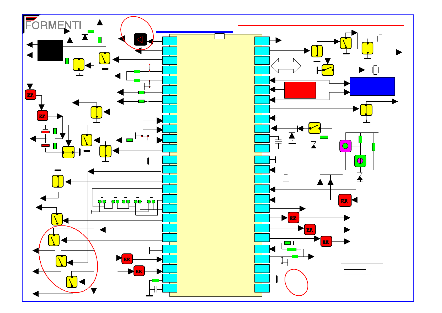
SOUND I.F.
CVBS
IC 204
TR200
TR201
F575
TO PIN 1
IC 204
F576
TR107
TO STEREO
NICAM
MODULE
TO PIN 4
IC 10
PIN 5
T
O
PIN 3
T
U
N
E
PIN 4
R
AM
SOUND
FILTER
F204
PIN 6
12V
TO PIN
10, 11
IC 200
TR210
TR2
TR 502
TR 501
TR218
TO PIN 4 IC 201
TO PIN 8 IC 201
TR110
TR209
TR503
12 V
TUNUNG
VOLTAGE
TO PIN 2
TUNER
TO X13
TR219
5V
FRON PIN 8 SCART 1
FROM PIN 8 SCART 2
5V
TR111
TO SWITC INT/EX SOUND
MENU V - V + P - P +
TV ON / OFF
CVBS FROM
ANTENNA
CVBS
FROM SCART
5V
TR500
R174
R128
R140
R146
TR203
TR211
SAA 5553
1
V TUN.
2
R141
DSC
3
SWT. L/L'
4
CTI STS.
5
16:9 STS
6
SWT. S1/S2
COPY SWT.
7
SWT. CI/S1
8
AV1 STS.
9
AV2 STS.
10
H.P. STS.
11
SYSTEM
12
VSS M+T
13
UHF
14
TV / AV
15
P0.3
16
P0.4
17
P0.5
18
ON / OFF
19
VHF H
20
VHF L
21
VSSA
22
CVBS0
23
CVBS1
24
BLACK
25
IREF
26
OSC. SWT.
INT. TEST
MICRO & TXT PERIPHERALS
SWT 16:9
MSDA
MSCL
SDA 1
INTO
SCL 1
AM/FM
VDDM
RESET
OSCOUT
OSCIN
OSCGND
VDDT
VSSA
VSYNC
HSYNC
BLK
R
G
B
RGBREF
PIP STS
COR
FRAME
52
51
50
49
48
47
46
45
44
43
42
41
40
39
38
37
36
35
34
33
32
31
30
29
28
27
TO CTI &
16:9 MOULE
IIC BUS
IRR100
SOUND STDANDARD SWITCH
TR 108
QZ100
TR 109
IIC BUS
3,3 V
D 105
12 MHz
3,3 V
D 108
D 102
TR 101
TR 102
TR 103
R167
5V
FOR VOLTAGE
SISTETIZER ONLY
TR206
TR 205
EEPROM
IC 101
TR8
TR7
D5
5 V
FLYBACK
FROM EHT
VERTICAL
BLANKING
FROM PIN 8
IC 5
TO PIN
23, 24, 25
IC 204
F19PAPER.DRW
E.G. 22 / 04 /2000
PAINTER
TR 208
3.58MHz
TR 105
R39
2,5V
4.43 MHz
TO
PIN 35
IC 204
TO PIN 10
IC 102
5 V
R40
Page 19

VIDEO
VIDEO
SIGNAL
SIGNAL
PROCESSING
PROCESSING
Page 20
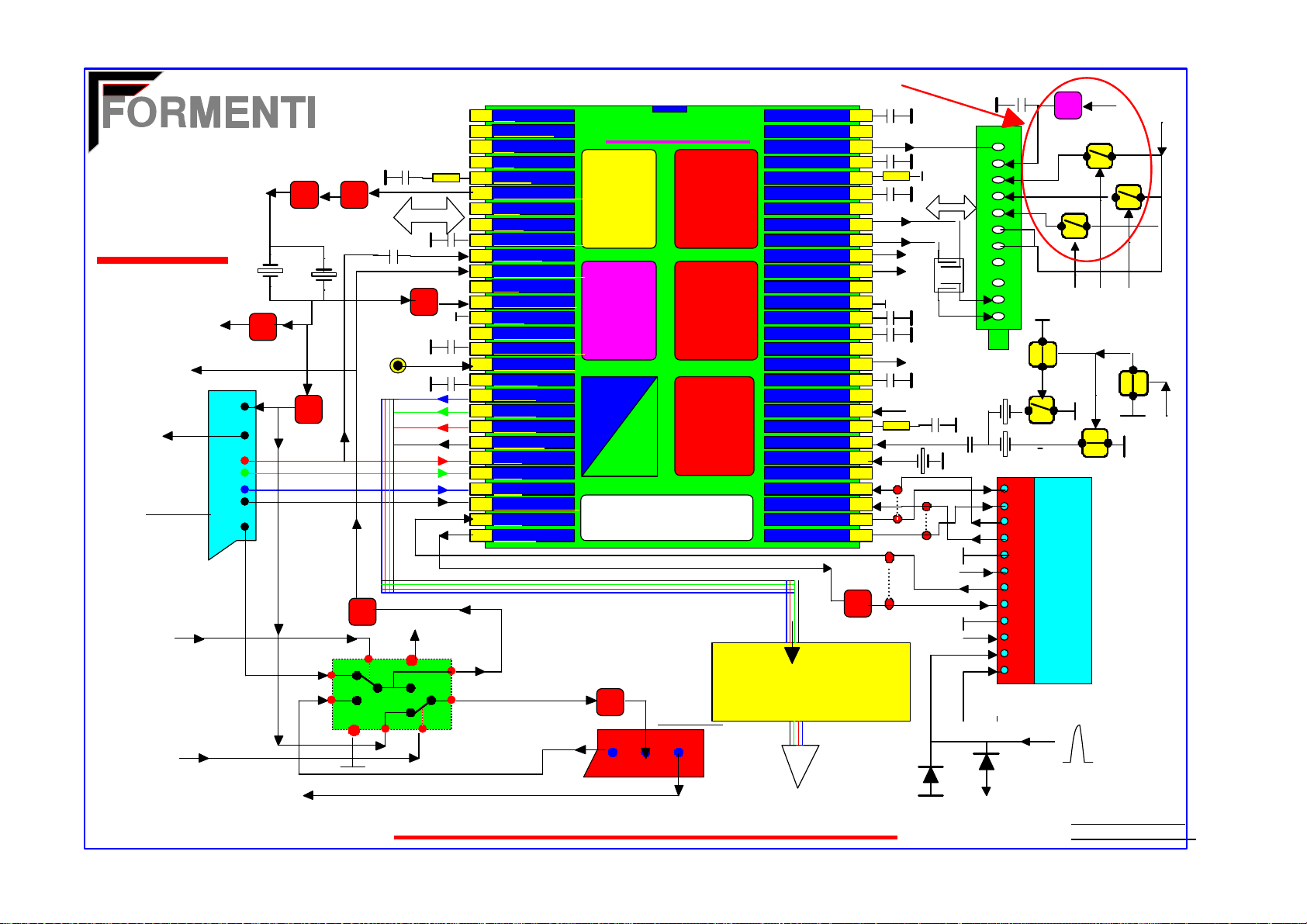
F 19
TO PIN 33
IC100
CVBS
FOR TXT
TO PIN 24
IC 100
(CVBS FOR TXT)
TO PIN 9
IC 100
AV1
STATUS
SCART 1
FROM PIN 6
IC100
AV1 / AV2
SWITCH
FROM PIN 7
IC100
AV1 / TV
SWITCH
TO AV2
EF
TR203
19
8
15
11
7
16
20
CVBS IN
TV
CVBS
TO PIN 10
IC 100
AV2 STATUS
TR201
EF
TR204
TR211
1
3
EFEF
TR200
EF
4
FOR VOLTAGE SINTHESIS ONLY
SIF
1
AUDEXT
VIDEO IN
CINCH
7
IIC
TR202
EF
12 V
6
82
2
NC
3
NC
4
PLLIF
5
IFVIDEO OUT
6
SCL
7
SDA
8
DECOUPLING
9
CHR.IN
10
EX.CVBS/Y IN
11
VP1
12
INT CVBS IN
13
GND
14
AUDIO OUT
15
DECOUPLING
16
EX. CVBS IN
17
BLKIN
18
B OUT
19
G OUT
20
R OUT
21
BCL/VG
22
R IN
23
G IN
24
B IN
25
RGB INSERT.
26
Y IN
27
Y OUT
28
5
9
1/3 0F IC201
LA7955
CVBS IN
CVBS OUT
TDA884X
I.F.
VIDEO
AGC
AFC
DEM.
IDENT
SOUND
PROCES.
(MONO)
SYNC
PROCES.
V. & H.
TIME
BASE
TRANSRECEIVER
TR212
EF
20 19
CONTROL
EXT RGB
IIC
SCART 2
8
MSD
PAL
(SECAM)
NTSC
C.D. &
RGB
MATRIX
VIDEO
SWITCH
& RGB
DRIVE
RGB AMPLIFIER
VIDEO SIGNAL PATH
DECOUPLING
DEENPHASIS
AGC OUT
DECOPLING
I REF
VERT. RAMP
EHT PROTEC.
IF IN 2
IF IN 1
V. DRIVE A
V. DRIVE B
E - W OUT
GND 2
PH. 1 FILTER
PH. 2 FILTER
H. IN, S.C. OUT
HOR. OUT
DECOUPLING
CVBS 1 OUT
V P 2
DET FILTER
X TAL 2
X TAL 1
S.C. REF OUT
R - Y IN
B - Y IN
R - Y OUT
B - Y OUT
MODULE
TO CRT
EF
TR500
56
55
54
53
52
51
50
49
48
47
46
45
44
43
42
41
40
39
38
37
36
35
34
33
32
31
30
29
8 V
UV
12 V
1
2
3
4
IIC
5
6
7
8
9
TR208
3.58MHz
3,57MHz
5 V
FROM PIN 52
IC 100 4:3 TO 16:9
SWITCH
10
11
A10
8 V
UHF
VHF H
VHF L
4.43MHz
1
2
3
4
5
6
7
8
9
10
11
12
TR206
C T I
&
4 : 3
TO
16 : 9
FROM PIN 1
∫∫
IC 100
TR501
TR503
TR502
FROM IC 100
PIN 14, 20, 21
BAND SWITCHING
TR105
TR205
FROM EHT
F19VIDEP.DRW
E.G. 14 / 11 / 99
5 V
FROM
PIN 51
IC 100
Page 21

Reset signal
The externally applied RESET signal (active HIGH) is used to initialize the microcontroller
core, in addition to the teletext decoder. However, the teletext decoder incorporates a
separate internal reset function which is activated on the rising edge of the analog supply
pin, VDDA . The purpose of this internal reset circuit is to initialize the teletext decoder when
returning from the “text standby mode”.
TDA884X FAMILY SPECIFICATION
FEATURES
The following features are available in all IC’s:
• Multi-standard vision IF circuit with an alignment-freePLL demodulator without external
components
• Alignment-free multi-standard FM sound demodulator(4.5 MHz to 6.5 MHz)
• Audio switch
• Flexible source selection with CVBS switch andY(CVBS)/C input so that a comb filter can
be applied
• Integrated chrominance trap circuit
• Integrated luminance delay line
• Asymmetrical peaking in the luminance channel with a(defeatable) noise coring function
• Black stretching of non-standard CVBS or luminancesignals
• Integrated chroma band-pass filter with switchablecentre frequency
• Dynamic skin tone control circuit
• Blue stretch circuit which offsets colours near whitetowards blue
• RGB control circuit with “Continuous CathodeCalibration” and white point adjustment
• Possibility to insert a “blue back” option when no videosignal is available
• Horizontal synchronization with two control loops andalignment-free horizontal
oscillatoroptimised N2 application.Functionally the IC series is split up is 3 categories,
viz:
E.G.Data creazione 01/11/99 17.27 13 / 30 F19MANU.doc
Page 22
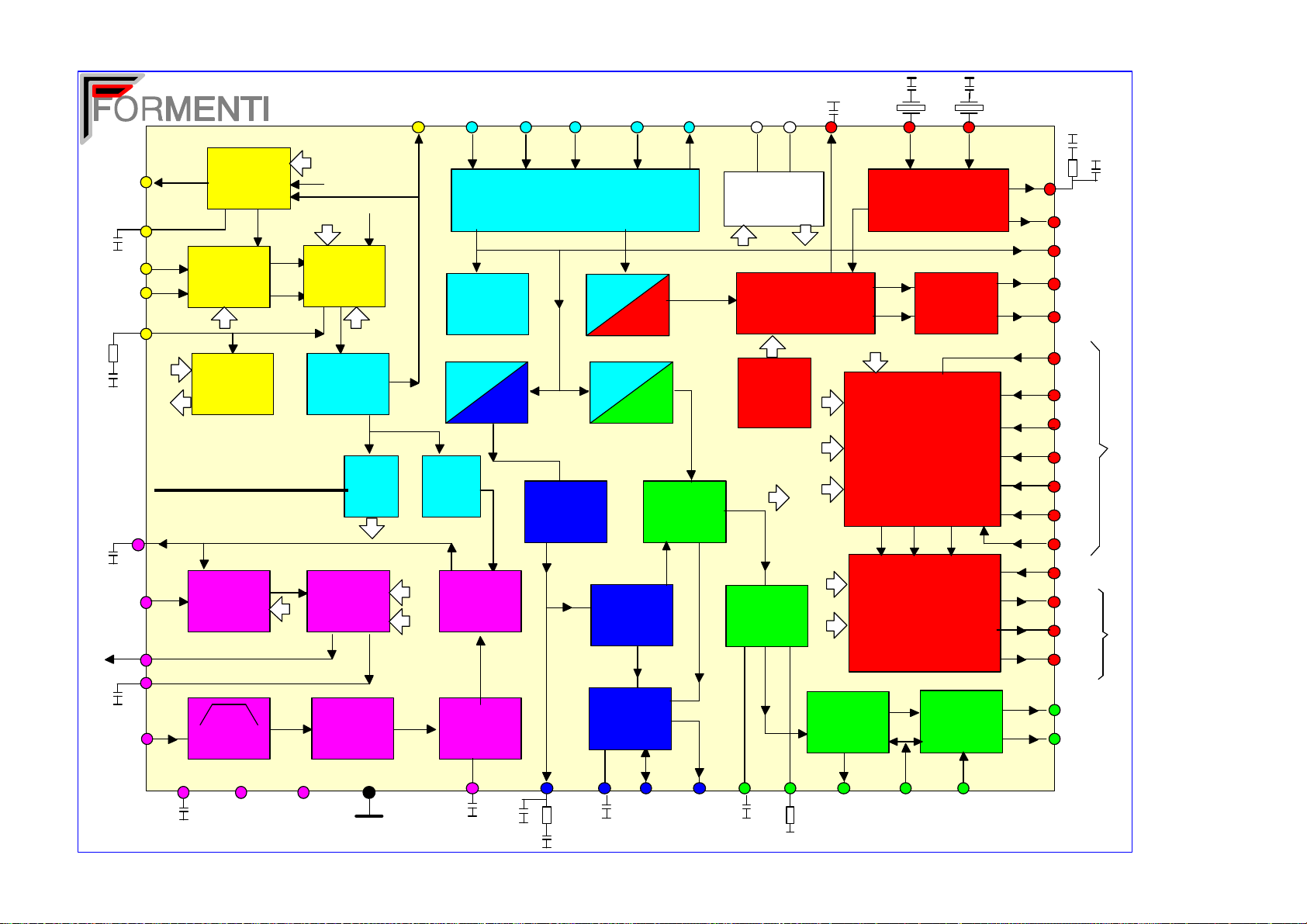
TUNER
AGC
I.F IN
PLL
FILTER
Deenphasis
EXTERNAL
AUDIO IN
54
53
IF &
TUNER
A G C
I.F. value
48
VIDEO IF
AMPLIFIER
49
Sensitivity
5
A
F
W
AFA
AFB
A F C
TDA 8844
55
DEENPHASIS LINE
Internal
Audio
EXTERNAL
2
AUDIO
SWITCH
15A.F.
MONO AUDIO OUTPUT
SWT
TUNER T.O.P
gating
calibration
PLL
DEMOD.
& VCO
VIDEO
AMPLIFIER
VIDEO
IDENT.
AVL
SWITCH &
VOLUME
CVBS OUTPUT
6
MOD
Pos./Neg.
AVL
Volume
CVBS (int) IN
CVBS (ext) IN
CVBS / Y IN
13 17 11 10
CVBS & Y/C
SWITCH
Luma
Y DELAY,
C. TRAP,
Y PEAKING
To Sync
H.
SYNC
SEPARATOR
VIDEO
MUTE
AUDIO PRE
AMPLIFIER
& MUTE
H. sync
PHI 1
DETECTOR
CHROMA IN
Chroma
CHROMA
CLOCHE &
BANDPASS
V. SYNC
SEPARATOR
VERTICAL
DEVIDER
LINE
OSCILL.
CVBS OUT
(comb filter)
38
V. sync
SCL SDA
7 8
IIC
TRANSRECEIVER
IIC
PAL / NTSC
SECAM
DECODER
AUTO
SYSTEM
IDENT.
MANAGER
VERTICAL
SAWTOOTH
GENERATOR
Secam
Decoupling
16
34 35
BURST PHASE
DETECTOR
Subcarrier
GAI
SAT
R-Y & B-Y
MATRIX
MAT
SAT CONTR.
BLACK STRETCH
DSA
SKIN TINT CORR.
RGB SWITCH
CON
RGB CONTROL
AUTO CUT-OFF
& OUTPUT
BRI
Xtal
& VCXO
BASE BAND
CHROMA
DELAY LINE
36
33
28
29
30
27
31
32
23
24
25
26
18
19
20
21
Loop
filter
Phase
Detector
Fsc
Y
B-Y
R-Y
Y
B-Y
R-Y
R
G
B
F.B.
Black
Currente
Input
R
G
B
I
N
P
U
T
O
U
T
P
U
T
AVL
Decoupling
INTERCARRIER
IN
BandGap
Decoupling
(45)
1
1 A 10 MHz
9
B.P.F.
Supply
12
AUDIO
LIMITER
37 14
8 V8 V Main
Supply
Ground
AUDIO
PLL DEM.
56
Sound
Decoupling
PHI 2
LINE OUT
S.C. GENER.
43 41 40
Phi 1
filter
42
Phi 2
filter
Flyback in
Sand
Castle
Out
51 52
Line
Pulse
Vertical
Out
Sawtooth Reference
E - W
GEOMETRY
45
E-W
DRIVE
VERTICAL
DRIVE
50
EHT
Overvoltage
47
46
22
V- Guard &
B.C. limiter
TDA8844BLDIA.DRW
E.G. 17 /10 / 99
Vertical
Drive
Output
Page 23

• Versions intended to be used in economy TV receiverswith all basic functions (envelope:
S-DIP 56 and QFP 64)
• Versions with additional features like E-W geometrycontrol, H-V zoom function and YUV
interface which are intended for TV receivers with 110° picture tubes(envelope: S-DIP 56)
• Versions which have in addition a second RGB inputwith saturation control and a second
CVBS output (envelope: QFP 64)
• Vertical count-down circuit
• Vertical driver optimised for DC-coupled vertical outputstages
GENERAL DESCRIPTION
The various versions of the TDA 884X/5X series areI 2 C-bus controlled single chip TV
processors which are
intended to be applied in PAL, NTSC, PAL/NTSC and multi-standard television receivers.
The N2 version is pin and application compatible with the N1 version, however,a new
feature has been added which makes the N2 more attractive. The IF PLL demodulator has
been replaced byan alignment-free IF PLL demodulator with internal VCO (no tuned circuit
required). The setting of the variousfrequencies (33.4, 33.9, 38, 38.9, 45,75 and 58.75
MHz) can be made via the I 2 C-bus.
Because of this difference the N2 version is compatiblewith the N1, however, N1 devices
cannot be used in an optimized N2 application
Functionally the IC series is split up is 3 categories, viz:
• Versions intended to be used in economy TV receivers with all basic functions (envelope:
S-DIP 56 and QFP 64)
• Versions with additional features like E-W geometry control, H-V zoom function and YUV
interface which areintended for TV receivers with 110° picture tubes (envelope: S-DIP 56)
• Versions which have in addition a second RGB input with saturation control and a
second CVBS output (envelope: QFP 64)
FUNCTIONAL DESCRIPTION
Vision IF amplifier
The IF-amplifier contains 3 ac-coupled control stages with a total gain control range which
is higher then 66 dB. The sensitivity of the circuit is comparable with that of modern
E.G.Data creazione 01/11/99 17.27 14 / 30 F19MANU.doc
Page 24

IF-IC’s.
The video signal is demodulated by means of an alignment-free PLL carrier regenerator
with an internalVCO. This VCO is calibrated by means of a digital control circuit which
uses the X-tal frequency of the colour decoder as a reference. The frequency setting for
the various standards (33.4, 33.9, 38, 38.9, 45.75 and 58.75 MHz) is realised via the I 2 Cbus. To get a good performance for phase modulated carrier signals the control speed of
the PLL can be increased by means of the FFI bit.
The AFC output is generated by the digital control circuit of the IF-PLL demodulator and
can be read via the I 2 C-bus.
For fast search tuning systems the window of the AFC can be increased with a factor 3.
The setting is realised with the AFW bit. The AFC data is valid only when the horizontal
PLL is in lock (SL = 1)
Depending on the type the AGC-detector operates on top-sync level (single standard
versions) or on top sync and top white- level (multi standard versions). The demodulation
polarity is switched via the I 2 C-bus. The AGC detector time-constant capacitor is
connected externally. This mainly because of the flexibility of the application. The timeconstant of the AGC system during positive modulation is rather long to avoid visible
variations of the signal amplitude. To improve the speed of the AGC system a circuit has
been included which detects whether the AGC detector is activated every frame period.
When during 3 field periods no action detected the speed of the system is increased. For
signals without peak white information the system switches automatically to a gated black
level AGC. Because a black level clamp pulse is required for this way of operation the
circuit will only switch to black level AGC in the internal mode.
The circuits contain a video identification circuit which is independent of the
synchronisation circuit. Therefore search tuning is possible when the display section of the
receiver is used as a monitor. However, this ident circuit cannot be made as sensitive as
the slower sync ident circuit (SL) and we recommend to use both ident outputs to obtain a
reliable search system. The ident output is supplied to the tuning system via the I 2 C-bus.
The input of the identification circuit is connected to pin 13 (S-DIP 56 devices), the
“internal” CVBS input (see Fig.6).
This has the advantage that the ident circuit can also be made operative when a
scrambled signal is received (descrambler connected between pin 6 (IF video output) and
pin 13). A second advantage is that the ident circuit can be used when the IF amplifier is
not used (e.g. with built-in satellite tuners).
E.G.Data creazione 01/11/99 17.27 15 / 30 F19MANU.doc
Page 25

The video ident circuit can also be used to identify the selected CBVS or Y/C signal. The
switching between the 2 modes can be realised with the VIM bit.
Video switches
The circuits have two CVBS inputs (internal and external CVBS) and a Y/C input. When
the Y/C input is not required the Y input can be used as third CVBS input. The switch
configuration is given in Fig.6. The selection of the various sources is made via the I 2 Cbus.
For the TDA 884X devices the video switch configuration is identical to the switch of the
TDA 8374/75 series. So the circuit has one CVBS output (amplitude of 2 VP-P for the
TDA884X series) and the I 2 C-bus control is similar to that of the TDA 8374/75. For the
TDA 885X IC’s the video switch circuit has a second output (amplitude of 1 VP-P ) which
can be set independently of the position of the first output. The input signal for the decoder
is also available on the CVBS1-output.
Therefore this signal can be used to drive the Teletext decoder. If S-VHS is selected for
one of the outputs the luminance and chrominance signals are added so that a CVBS
signal is obtained again.
Sound circuit
The sound bandpass and trap filters have to be connected externally. The filtered
intercarrier signal is fed to a limiter circuit and is demodulated by means of a PLL
demodulator. This PLL circuit tunes itself automatically to the incoming carrier signal so
that no adjustment is required.
The volume is controlled via the I 2 C-bus. The deemphasis capacitor has to be connected
externally. The non-controlled audio signal can be obtained from this pin (via a buffer
stage).
The FM demodulator can be muted via the I 2 C-bus. This function can be used to switchoff the sound during a channel change so that high output peaks are prevented.
The TDA 8840/41/42/46 contain an Automatic Volume Levelling (AVL) circuit which
automatically stabilises the audio output signal to a certain level which can be set by the
viewer by means of the volume control. This function prevents big audio output fluctuations
due to variations of the modulation depth of the transmitter. The AVL function can be
activated via the I 2 C-bus.
Synchronisation circuit
E.G.Data creazione 01/11/99 17.27 16 / 30 F19MANU.doc
Page 26

The sync separator is preceded by a controlled amplifier which adjusts the sync pulse
amplitude to a fixed level. These pulses are fed to the slicing stage which is operating at
50% of the amplitude. The separated sync pulses are fed to the first phase detector and to
the coincidence detector. This coincidence detector is used to detect whether the line
oscillator is synchronised and can also be used for transmitter identification. This circuit
can be made less sensitive by means of the STM bit. This mode can be used during
search tuning to avoid that the tuning system will stop at very weak input signals. The first
PLL has a very high statical steepness so that the phase of the picture is independent of
the line frequency.
The horizontal output signal is generated by means of an oscillator which is running at
twice the line frequency. Its frequency is divided by 2 to lock the first control loop to the
incoming signal. The time-constant of the loop can be forced by the I 2 C-bus (fast or
slow). If required the IC can select the time-constant depending on the noise content of the
incoming video signal.
The free-running frequency of the oscillator is determined by a digital control circuit which
is locked to the reference signal of the colour decoder. When the IC is switched-on the
horizontal output signal is suppressed and the oscillator is calibrated as soon as all subaddress bytes have been sent. When the frequency of the oscillator is correct the
horizontal drive signal is switched-on. To obtain a smooth switching-on and switching-off
behaviour of the horizontal output stage the horizontal output frequency is doubled during
switch-on and switch-off (slow start/stop). During that time the duty cycle of the output
pulse has such a value that maximum safety is obtained for the output stage.
To protect the horizontal output transistor the horizontal drive is immediately switched off
when a power-on-reset is detected. The drive signal is switched-on again when the normal
switch-on procedure is followed, i.e. all sub-address bytes must be sent and after
calibration the horizontal drive signal will be released again via the slow start procedure.
When the coincidence detector indicates an out-of-lock situation the calibration procedure
is repeated.
The circuit has a second control loop to generate the drive pulses for the horizontal driver
stage. The horizontal output is gated with the flyback pulse so that the horizontal output
transistor cannot be switched-on during the flyback time.
Via the I 2 C-bus adjustments can be made of the horizontal and vertical geometry. The
vertical sawtooth generator drives the vertical output drive circuit which has a differential
output current. For the E-W drive a single ended current output is available. A special
E.G.Data creazione 01/11/99 17.27 17 / 30 F19MANU.doc
Page 27

feature is the zoom function for both the horizontal and vertical deflection and the vertical
scroll function which are available in some versions. When the horizontal scan is reduced
to display 4:3 pictures on a 16:9 picture tube an accurate video blanking can be switched
on to obtain well defined edges on the screen.
Overvoltage conditions (X-ray protection) can be detected via the EHT tracking pin. When
an overvoltage condition is detected the horizontal output drive signal will be switched-off
via the slow stop procedure but it is also possible that the drive is not switched-off and that
just a protection indication is given in the I 2 C-bus output byte.
The choice is made via the input bit PRD. The IC’s have a second protection input on the
ϕ2 filter capacitor pin. When this input is activated the drive signal is switched-off
immediately and switched-on again via the slow start procedure. For this reason this
protection input can be used as “flash protection”.
The drive pulses for the vertical sawtooth generator are obtained from a vertical
countdown circuit. This countdown circuit has various windows depending on the incoming
signal (50 Hz or 60 Hz and standard or non standard). The countdown circuit can be
forced in various modes by means of the I 2 C-bus. During the insertion of RGB signals
the maximum vertical frequency is increased to 72 Hz so that the circuit can also
synchronise on signals with a higher vertical frequency like VGA. To obtain short switching
times of the countdown circuit during a channel change the divider can be forced in the
search window by means of the NCIN bit. The vertical deflection can be set in the deinterlace mode via the I 2 C bus. To avoid damage of the picture tube when the vertical
deflection fails the guard output current of the TDA 8350/51 can be supplied to the beam
current limiting input. When a failure is detected the RGB-outputs are blanked and a bit is
set (NDF) in the status byte of the I 2 C-bus. When no vertical deflection output stage is
connected thisguard circuit will also blank the output signals. This can be overruled by
means of the EVG bit.
Chroma and luminance processing
The circuits contain a chroma bandpass and trap circuit. The filters are realised by means
of gyrator circuits and
they are automatically calibrated by comparing the tuning frequency with the X-tal
frequency of the decoder. The luminance delay line and the delay for the peaking circuit
are also realised by means of gyrator circuits. The centre frequency of the chroma
bandpass filter is switchable via the I 2 C-bus so that the performance can be optimised for
E.G.Data creazione 01/11/99 17.27 18 / 30 F19MANU.doc
Page 28

“front-end” signals and external CVBS signals. During SECAM reception the centre
frequency of the chroma trap is reduced to get a better suppression of the SECAM carrier
frequencies. All IC’s have a black stretcher circuit which corrects the black level for
incoming video signals which have a deviation between the black level and the blanking
level (back porch). The timeconstant for the black stretcher is realised internally.
The resolution of the peaking control DAC has been increased to 6 bits. All IC’s have a
defeatable coringfunction in the peaking circuit. Some of these IC’s have a YUV interface
(see table on page 2) so that picture improvement IC’s like the TDA 9170 (Contrast
improvement), TDA 9177 (Sharpness improvement) and TDA 4556/66 (CTI) can be
applied. When the CTI IC’s are applied it is possible to increase the gain of the luminance
channel by means of the GAI bit in subaddress 03 so that the resulting RGB output signals
are not affected.
Colour decoder
Depending on the IC type the colour decoder can decode PAL, PAL/NTSC or
PAL/NTSC/SECAM signals. The PAL/NTSC decoder contains an alignment-free X-tal
oscillator, a killer circuit and two colour difference demodulators. The 90° phase shift for
the reference signal is made internally.
The IC’s contain an Automatic Colour Limiting (ACL) circuit which is switchable via the I 2
C-bus and which prevents that oversaturation occurs when signals with a high chroma-toburst ratio are received. The ACL circuit is designed such that it only reduces the chroma
signal and not the burst signal. This has the advantage that the colour sensitivity is not
affected by this function. The SECAM decoder contains an auto-calibrating PLL
demodulator which has two references, viz: the 4.4 MHz sub-carrier frequency which is
obtained from the X-tal oscillator which is used to tune the PLL to the desired free-running
frequency and the bandgap reference to obtain the correct absolute value of the output
signal. The VCO of the PLL is calibrated during each vertical blanking period, when the IC
is in search or SECAM mode.
The frequency of the active X-tal is fed to the Fsc output (pin 33) and can be used to tune
an external comb filter (e.g. the SAA 4961).
The base-band delay line (TDA 4665 function) is integrated in the PAL/SECAM IC’s and in
the NTSC IC TDA 8846A. In the latter IC it improves the cross colour performance
(chroma comb filter). The demodulated colour difference signals are internally supplied to
the delay line. The colour difference matrix switches automatically between PAL/SECAM
and NTSC, however, it is also possible to fix the matrix in the PAL standard.
E.G.Data creazione 01/11/99 17.27 19 / 30 F19MANU.doc
Page 29

The “blue stretch” circuit is intended to shift colour near “white” with sufficient contrast
values towards more blue to obtain a brighter impression of the picture.
Which colour standard the IC’s can decode depends on the external X-tals. The X-tal to be
connected to pin 34 must have a frequency of 3.5 MHz (NTSC-M, PAL-M or PAL-N) and
pin 35 can handle X-tals with a frequency of 4.4 and 3.5 MHz. Because the X-tal frequency
is used to tune the line oscillator the value of the X-tal frequency must be given to the IC
via the I 2 C-bus. It is also possible to use the IC in the so called “Tri-norma” mode for
South America. In that case one X-tal must be connected to pin 34 and the other 2 to pin
35. The switching between the 2 latter X-tals must be done externally. This has the
consequence that the search loop of the decoder must be controlled by the µ-computer.
To prevent calibration problems of the horizontal oscillator the external switching between
the 2 X-tals should be carried out when the oscillator is forced to pin 34. For a reliable
calibration of the horizontal oscillator it is very important that the X-tal indication bits (XA
and XB) are not corrupted. For this reason the X-tal bits can be read in the output bytes so
that the software can check the I 2 C-bus transmission.
Under bad-signal conditions (e.g. VCR-playback in feature mode), it may occur that the
colour killer is activated although the colour PLL is still in lock. When this killing action is
not wanted it is possible to overrule the colour killer by forcing the colour decoder to the
required standard and to activate the FCO-bit (Forced Colour On) in the control-5
subaddress.
The IC’s contain a so-called “Dynamic skin tone (flesh) control” feature. This function is
realised in the YUV domain by detecting the colours near to the skin tone. The correction
angle can be controlled via the I 2 C-bus.
RGB output circuit and black-current stabilisation
The colour-difference signals are matrixed with the luminance signal to obtain the RGBsignals. The TDA 884X devices have one (linear) RGB input. This RGB signal can be
controlled on contrast and brightness (like TDA 8374/75). By means of the IE1 bit the
insertion blanking can be switched on or off. Via the IN1 bit it can be read whether the
insertion pin has a high level or not.
The TDA 885X IC’s have an additional RGB input. This RGB signal can be controlled on
contrast, saturation and brightness. The insertion blanking of this input can be switched-off
by means of the IE2 bit. Via the IN2 bit it can be read whether the insertion pin has a high
level or not.
E.G.Data creazione 01/11/99 17.27 20 / 30 F19MANU.doc
Page 30

The output signal has an amplitude of about 2 volts black-to-white at nominal input signals
and nominal settings of the controls. To increase the flexibility of the IC it is possible to
insert OSD and/or teletext signals directly at the RGB outputs. This insertion mode is
controlled via the insertion input (pin 26 in the S-DIP 56- and pin 38 in the QFP-64
envelope). This blanking action at the RGB outputs has some delay which must be
compensated externally.
To obtain an accurate biasing of the picture tube a “Continuous Cathode Calibration”
circuit has been developed. This function is realised by means of a 2-point black level
stabilisation circuit. By inserting 2 test levels for each gun and comparing the resulting
cathode currents with 2 different reference currents the influence of the picture tube
parameters like the spread in cut-off voltage can be eliminated.
This 2-point stabilisation is based on the principle that the ratio between the cathode
currents is coupled to the ratio between the drive voltages according to:
[ I
The feedback loop makes the ratio between the cathode currents Ik1 and Ik2 equal to the
ratio between the reference currents (which are internally fixed) by changing the (black)
level and the amplitude of the RGB output signals via 2 converging loops. The system
operates in such a way that the black level of the drive signal is controlled to the cut-off
point of the gun so that a very good grey scale tracking is obtained. The accuracy of the
adjustment of the black level is just dependent on the ratio of internal currents and these
can be made very accurately in integrated circuits. An additional advantage of the 2-point
measurement is that the control system makes the absolute value of Ik1 and Ik2 identical
to the internal reference currents. Because this adjustment is obtained by means of an
adaption of the gain of the RGB control stage this control stabilises the gain of the
complete channel (RGB output stage and cathode characteristic).
As a result variations in the gain figures during life will be compensated by this 2-point
loop.
ki
/ I
k2 ]
= [ V
dr1
/ V
dr2
]
An important property of the 2-point stabilisation is that the off-set as well as the gain of
the RGB path is adjusted by the feedback loop. Hence the maximum drive voltage for the
cathode is fixed by the relation between the test pulses, the reference current and the
relative gain setting of the 3 channels. This has the consequence that the drive level of the
CRT cannot be adjusted by adapting the gain of the RGB output stage. Because different
picture tubes may require different drive levels the typical “cathode drive level” amplitude
can be adjusted by means of an I 2 C-bus setting. Dependent on the chosen cathode drive
E.G.Data creazione 01/11/99 17.27 21 / 30 F19MANU.doc
Page 31

level the typical gain of the RGB output stages can be fixed taking into account the drive
capability of the RGB outputs (pins 19 to 21). More details about the design will be given in
the application report.
The measurement of the “high” and the “low” current of the 2- point stabilisation circuit is
carried out in 2 consecutive fields. The leakage current is measured in each field. The
maximum allowable leakage current is 100 µA When the TV receiver is switched-on the
RGB output signals are blanked and the black current loop will try to set the right picture
tube bias levels. Via the AST bit a choice can be made between automatic start-up or a
start-up via the µ-processor. In the automatic mode the RGB drive signals are switched-on
as soon as the black current loop
has been stabilised. In the other mode the BCF bit is set to 0 when the loop is stabilised.
The RGB drive can than be switched-on by setting the AST bit to 0. In the latter mod some
delay can be introduced between the setting of the BCF bit and the switching of the AST
bit so that switch-on effects can be suppressed. It is also possible to start-up the devices
with a fixed internal delay (as with the TDA 837X and the TDA884X/5X N1). This mode is
activated with the BCO bit.
The vertical blanking is adapted to the incoming CVBS signal (50 Hz or 60 Hz). When the
flyback time of the vertical output stage is longer than the 60 Hz blanking time the blanking
can be increased to the same value as that of the 50 Hz blanking. This can be set by
means of the LBM bit.
For an easy (manual) adjustment of the Vg2 control voltage the VSD bit is available. When
this bit is activated the black current loop is switched-off, a fixed black level is inserted at
the RGB outputs and the vertical scan is switched-off so that a horizontal line is displayed
on the screen. This line can be used as indicator for the Vg2 adjustment. Because of the
different requirements for the optimum cut-off voltage of the picture tube the RGB output
level is adjustable when the VSD bit is activated. The control range is 2.5 ± 0.7 V and can
be controlled via the brightness control DAC. It is possible to insert a so called “blue back”
back-ground level when no video is available. This feature can be activated via the BB bit
in the control2 subaddress.
E.G.Data creazione 01/11/99 17.27 22 / 30 F19MANU.doc
Page 32
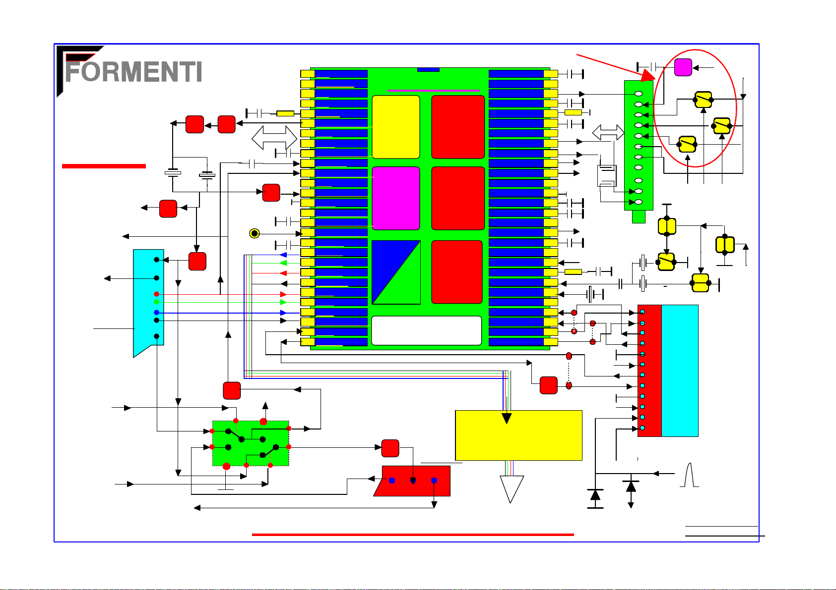
F 19
TO PIN 33
IC100
CVBS
FOR TXT
TO PIN 24
IC 100
(CVBS FOR TXT)
TO PIN 9
IC 100
AV1
STATUS
SCART 1
FROM PIN 6
IC100
AV1 / AV2
SWITCH
FROM PIN 7
IC100
AV1 / TV
SWITCH
TO AV2
EF
TR203
19
8
15
11
7
16
20
CVBS IN
TV
CVBS
TO PIN 10
IC 100
AV2 STATUS
TR201
EF
TR204
TR211
1
3
EFEF
TR200
EF
4
FOR VOLTAGE SINTHESIS ONLY
SIF
1
AUDEXT
VIDEO IN
CINCH
7
IIC
TR202
EF
12 V
6
82
2
NC
3
NC
4
PLLIF
5
IFVIDEO OUT
6
SCL
7
SDA
8
DECOUPLING
9
CHR.IN
10
EX.CVBS/Y IN
11
VP1
12
INT CVBS IN
13
GND
14
AUDIO OUT
15
DECOUPLING
16
EX. CVBS IN
17
BLKIN
18
B OUT
19
G OUT
20
R OUT
21
BCL/VG
22
R IN
23
G IN
24
B IN
25
RGB INSERT.
26
Y IN
27
Y OUT
28
5
9
1/3 0F IC201
LA7955
CVBS IN
CVBS OUT
TDA884X
I.F.
VIDEO
AGC
AFC
DEM.
IDENT
SOUND
PROCES.
(MONO)
SYNC
PROCES.
V. & H.
TIME
BASE
TRANSRECEIVER
TR212
EF
20 19
CONTROL
EXT RGB
IIC
SCART 2
8
MSD
PAL
(SECAM)
NTSC
C.D. &
RGB
MATRIX
VIDEO
SWITCH
& RGB
DRIVE
RGB AMPLIFIER
VIDEO SIGNAL PATH
DECOUPLING
DEENPHASIS
AGC OUT
DECOPLING
I REF
VERT. RAMP
EHT PROTEC.
IF IN 2
IF IN 1
V. DRIVE A
V. DRIVE B
E - W OUT
GND 2
PH. 1 FILTER
PH. 2 FILTER
H. IN, S.C. OUT
HOR. OUT
DECOUPLING
CVBS 1 OUT
V P 2
DET FILTER
X TAL 2
X TAL 1
S.C. REF OUT
R - Y IN
B - Y IN
R - Y OUT
B - Y OUT
MODULE
TO CRT
EF
TR500
56
55
54
53
52
51
50
49
48
47
46
45
44
43
42
41
40
39
38
37
36
35
34
33
32
31
30
29
8 V
UV
12 V
1
2
3
4
IIC
5
6
7
8
9
TR208
3.58MHz
3,57MHz
5 V
FROM PIN 52
IC 100 4:3 TO 16:9
SWITCH
10
11
A10
8 V
UHF
VHF H
VHF L
4.43MHz
1
2
3
4
5
6
7
8
9
10
11
12
TR206
C T I
&
4 : 3
TO
16 : 9
FROM PIN 1
∫∫
IC 100
TR501
TR503
TR502
FROM IC 100
PIN 14, 20, 21
BAND SWITCHING
TR105
TR205
FROM EHT
F19VIDEP.DRW
E.G. 14 / 11 / 99
5 V
FROM
PIN 51
IC 100
Page 33
IC204 TDA884X
F19 RGB AMPLIFIER
26 19/20/21
23/24/25
RGB
IN
FAST
BLK.
IN
RGB IN FROM SCART
RGB
OUT
R215
R216
R217
18
4 / 5 / 6
2
R17,R18,R19
R600
D800, D801, D802
R613
R614
R615
12 V
13
6/11/14
9/12/15
1/3/4
E.F.
200 V
52
TO G1 TRC
7/10/13
TO
RGB
KATODE
F19 RGBCO.DRW
E.G. 14 / 11 /99
3 X
R604
R605
R606
STV 5112
Page 34

F 19 FEATURE MODULE
Colour Transient Improvment
&
4 : 3 to 16 : 9 Signal Processing
Page 35

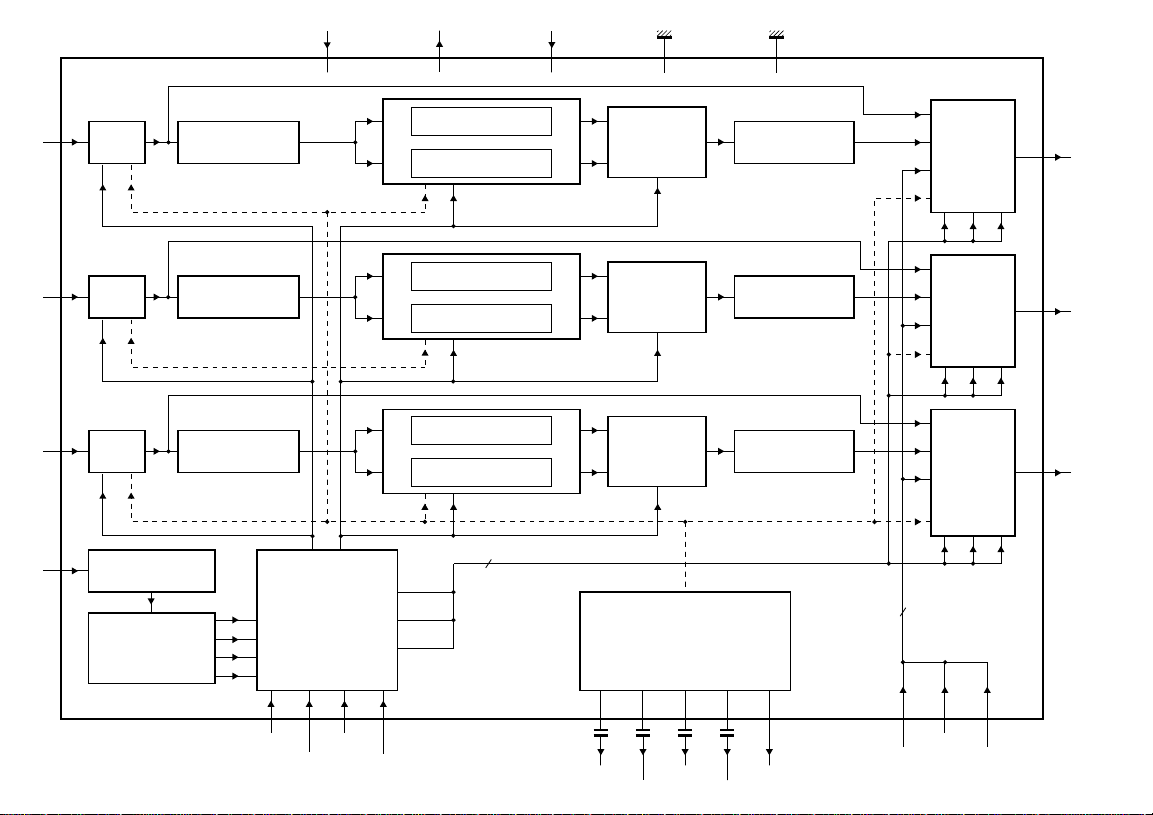
SAA4981
Monolithic integrated 16 : 9
Compressor
FEATURES
• Fixed horizontal compression by a factor of 4 ¤3 for most video standards
• Three fixed screen positions (left, centre and right)
• 5 MHz bandwidth
• Bypass function
• Inputs for luminance and chrominance of side panels
• Standard video inputs and outputs (Y, (Β-Y) and (Ρ-Y))
• Horizontal and vertical sync signals are not processed
• Pre filters and post filters on chip.
GENERAL DESCRIPTION
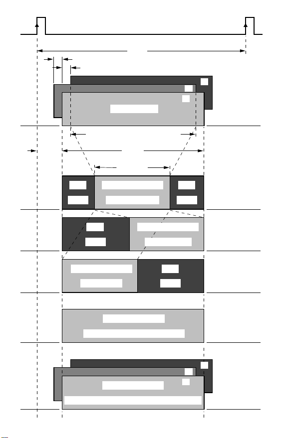
The integrated 16 : 9 compressor is an IC which compresses the active part of a video line
by a factor of 4 ¤3 from, for example, 52 ms to 39ms. This is necessary to display 4:3
video software on a 16 : 9 tube in the correctproportion. The capacitively coupled video
inputs are Y, (Β-Y) and (Ρ-Y).
The synchronisation input HREF is a line frequencyreference signal. The bandwidth of the
IC is up to 5 MHz and the signal delay is realized with SC Line Memories (Switched
Capacitors Line Memories). The output of the 16 : 9 compressor also has the format Y,
(Β Y) and (Ρ-Y) and provides the following two possibilities:
1. Bypass function (the input signal is not compressed)
2. Compressed video by a factor of 4 ¤3 with three different fixed screen positions (left,
centre and right). The luminance and chrominance of the side panels are determined by
the external signals YSIDE, BYSIDE and RYSIDE.
The horizontal compression is a time discrete and amplitude continuous signal processing.
This provides pre and post filters which are realized on-chip.
FUNCTIONAL DESCRIPTION
SAA4981 16:9 TO 4:3 PROCESSOR Pagina 1 di 3 e.g.SAA4981R.doc
Page 36
V
CCA
20 19 8 7 4
V
EEA
V
CCD
V
EED
SUB
YIN
HREF
23
22
21
6
CLAMP
CLAMP
CLAMP
HORIZONTAL
SEPARATION
54 MHz
PLL
5 MHz
LOW-PASS FILTER
5 MHz
LOW-PASS FILTER
5 MHz
LOW-PASS FILTER
CONTROLLER
SC LINE MEMORY
SC LINE MEMORY
SC LINE MEMORY
SC LINE MEMORY
SC LINE MEMORY
SC LINE MEMORY
C1
C2
C3
MUX
SC LINE
MEMORIES
6.7 MHz
LOW-PASS FILTER
MUX Y
18
YOUT
SAA4981
C1 C2 C3
MUX
SC LINE
MEMORIES
MUX
SC LINE
MEMORIES
3
CLAMP REFERENCE
6.7 MHz
LOW-PASS FILTER
6.7 MHz
LOW-PASS FILTER
C1 C2 C3
C1 C2 C3
3
MUX BY
MUX RY
17
(B-Y)OUT
16
(R-Y)OUT
TEST CTRL2
CTRL1 CTRL3
11 1 2 3 24 5 15 14 1310912
BYSIDE
C
LMY
C
LMBY
C
LMRY
BGREF
CLAOUT
YSIDE
RYSIDE
MHA277
Page 37

Applicable video standards
The integrated 16 : 9 compressor can be used for the following video standards; B, C, D,
G, H, I, K, K1, L, M and N. standards D, I, K, K1 and L will show a reducedvideo bandwidth
above 5 MHz.
Clamping circuit
The clamping circuits clamp the video input signals Y, (Β-Y) and (Ρ-Y) to the DC level of
the clamp reference signal fed from the clamp reference circuit. This is necessary to
ensure that the input signals are in the correct input voltage range for the 5 MHz low-pass
filters and the SC line memories.
Internal pre filters
Before the signals are sampled in the time discrete and amplitude continuous area, lowpass filtering is necessary to avoid any aliasing. Even if the inputs have already been lowpass filtered further filtering is advantageous for the electromagnetic compatibility (EMC).
The same transfer function is used for all three low-pass filters because of the same
bandwidth for the luminance and chrominance signals (up to 5 MHz)
SC line memories
After the low-pass filters the input signals are fed to the SC line memories. The signals are
sampled at a clock frequency of 13.5 MHz. One video line later the signals are read with a
clock frequency of 18 MHz in the compression mode. The result of the different clock
frequencies is a horizontal compression by a factor of 4 ¤3 . The clocks and the horizontal
starting pulses for the SC line memories are fed from the controller.
Two line memories are required for each signal path because in the compression mode, in
one video line the signals are sampled to the SC line memories with 13.5 MHz and one
video line later the signals are read with 18 MHz. In the bypass mode, via the SC line
memories, in one video line the signals are sampled with 13.5 MHz and one video line
later the signals are read with 13.5 MHz.
The SC line memories are suitable for signals with a bandwidth up to 5 MHz. With a
multiplexer (MUX) behind the SC line memories, the sampled video signal is connected to
the internal post filters.
Output multiplexer MUX Y, MUX (Β-Y) and MUX (Ρ-Y)
SAA4981 16:9 TO 4:3 PROCESSOR Pagina 2 di 3 e.g.SAA4981R.doc
Page 38

The output multiplexers are controlled via C1 and C2 fed from the controller. The
multiplexers are used to connect one of the four input signals to the output and, also,
enable fast switching.
The input signals of the multiplexers for one component
• The output signal of the post filter
• The uncompressed signal after the input clamping
• The clamping reference signal
• The signal for the side panel determined by YSIDE, BYSIDE and RYSIDE.
The horizontal separation circuit
The 54 MHz horizontal PLL is locked to the positive edge of the digital HREF signal, which
is generated in the positive edge of the burst key of a sandcastle signal.
54 MHz horizontal PLL
The 13.5 MHz clock frequency for the sampling clock and the 18 MHz clock frequency for
the reading clock are generated in the 54 MHz horizontal PLL. The 13.5 MHzclock and the
18 MHz clock are line locked.
Clamp reference
Reference voltages are generated In the clamp reference block. These DC signals are
used in the clamping circuits as input signals for the output multiplexers and as reference
voltages for the SC line memories. Four external capacitors at the pins CLMY , CLMBY ,
CLMRY and BGREF respectively are necessary to provide smoothing for the reference
voltages. A black level reference signal is available at CLAOUT.
Controller
The controller generates the clocks and the horizontal start signals for the SC line
memories and, also, the control signals for the output multiplexers. The timing for the start
reading signal for three different screen positions (left, centre and right) and the control
signals for the multiplexers (C1 and C2) is fixed. For the uncompressed signals a bypass
via the SC line memories and a bypass not via the SC line memories is available. When
the signals do not pass the line memories, the frequencyresponse is not affected by the sifunction.
SAA4981 16:9 TO 4:3 PROCESSOR Pagina 3 di 3 e.g.SAA4981R.doc
Page 39
HREF
6.3 µs
1.5 µs
64 µs
1.5 µs
sampled video
49 µs (used for compression)
52 µs
36.75 µs
side
panel
compressed video
(centre position)
side
panel
compressed video
(right position)
compressed video
(left position)
bypassed video
(bypass via the Line Memories)
side
panel
(2)
(1)
side
panel
(2)
(2)
bypassed video
(1)
(full bypass not through the Line Memories)
(2)
MHA278
Page 40

TDA4566
Colour transient improvement circuit
GENERAL DESCRIPTION
The TDA4566 is a monolithic integrated circuit for colour-transient improvement (CTI) and
luminance delay line in gyrator technique in colour television receivers.
Features
• Colour transient improvement for colour difference signals (R-Y) and (B-Y) with transient
detecting-, storage- and switching stages resulting in high transients of colour difference
output signals
• A luminance signal path (Y) which substitutes the conventional Y-delay coil with an
integrated Y-delay line
• Switchable delay time from 550 ns to 820 ns in steps of 90 ns and additional fine
adjustment of 37 ns
• Two Y output signals; one of 180 ns less delay
TDA4566 CTI Pagina 1 di 1
e.g.TDA4566R.doc
Page 41
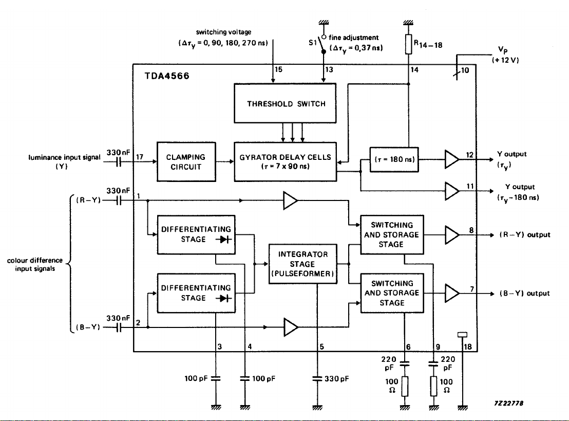
Page 42
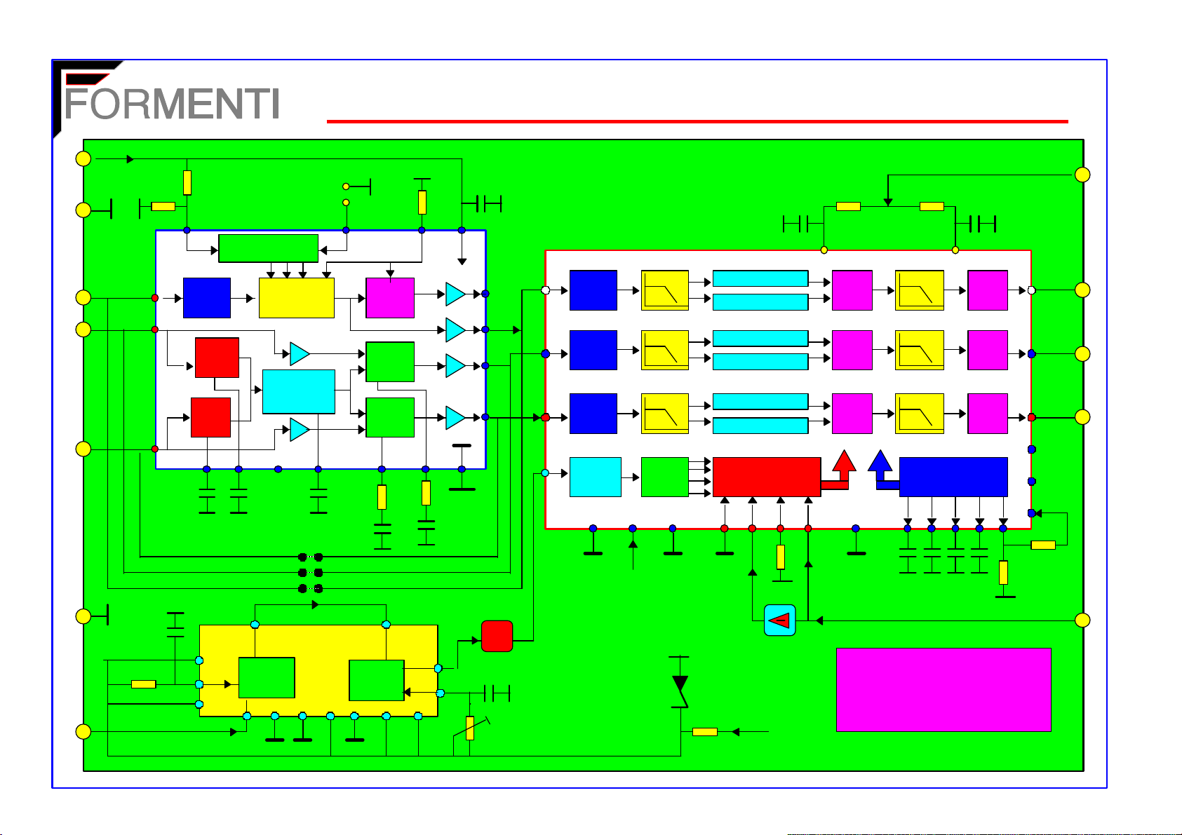
F19 CTI & 16:9 TO 4 : 3 COMPRESSOR
6
9
8
1
5
11
10
12 V
5 V
IC2 TDA4566
15 13
Y
17
R-Y
2
1
B-Y
2 3 4 5 6 9 18
8 V
R4
S.C INPUT
CLAMP
dV/dt
dV/dt
C10
16
14
13
THESHOLD SWT.
GYRATOR
DELAY CELLS
7 x 90 ns
INTEGRATOR
& PULSE
FORMER
JS 7
JS 6
JS 5
DUAL MONOSTABLE
MULTIVIBRATOR
M.M. M.M.
15
14 10
t = 180 ns
SWT. &
STORE
SWT. &
STORE
3 5168 1
10
12
Y
11
R-Y
8
B-Y
7
T2
EF
C9
IC 4 HEF 4538
2
R2
IC 1 SAA4981
23
22
21
6
H REF
CLAMP
CLAMP
CLAMP
HOR.
SEPAR.
LPF LPF
LPF LPF
LPF LPF
54 MHz
PLL
5 V
8 V
LINE MEMORY
LINE MEMORY
LINE MEMORY
LINE MEMORY
LINE MEMORY
LINE MEMORY
CONTROLLER
1247 20 19 1 2 3 524
D1
11 10 9
TR1
12 V
20
MUX MUX
MUX MUX
MUX MUX
CLAMP
REFERENCE
16:9 TO 4:3 SWITCH SIGNAL
note:
If CTI ( IC 2 TDA4566 IS NOT
PRESENT THAN JS 5, JS 6 & JS7
MUST BE INSERTED
8
F19FEAT.DRW
E.G. 12/12/99
13
15
18
17
16
14
Y OUT
R-Y
OUT
B-Y
OUT
7
4
3
12
Page 43

SCANNING
SCANNING
SECTION
SECTION
Page 44

TDA8351
DC-coupled vertical deflection
Circuit
FEATURES
Few external components
Highly efficient fully DC-coupled vertical output bridge circuit
Vertical flyback switch
Guard circuit
Protection against:
• short-circuit of the output pins (7 and 4)
• short-circuit of the output pins to VP
• Temperature (thermal) protection
• High EMC immunity because of common mode inputs
• A guard signal in zoom mode.
•
GENERAL DESCRIPTION
The TDA8351 is a power circuit for use in 9and 11 colour deflection systems for
field frequencies of 50 to 120 Hz. The circuit provides a DC driven vertical deflection
output circuit, operating as a highly efficient class G system.
FUNCTIONAL DESCRIPTION
The vertical driver circuit is a bridge configuration. The deflection coil is connected
between the output amplifiers, which are driven in phase opposition. An external resistor
(RM ) connected in series with the deflection coil provides internal feedback information.
The differential input circuit is voltage driven. The input circuit has been adapted to enable
it to be used with the TDA9150, TDA9151B, TDA9160A, TDA9162, TDA8366 and
TDA8376 which deliver symmetrical current signals. An external resistor (RCON )
connected between the differential input determines the output current through the
deflection coil.
TDA8351 VERTICAL OUTPUT Pagina 1 di 2 e.g.TDA8351R
Page 45

The relationship between the differential input current and the output current is defined by:
Idiff RCON =Icoil RM .
The output current is adjustable from 0.5 A (p-p) to 3 A(p-p) by varying RM . The maximum
input differential voltage is 1.8 V. In the application it is recommended that Vdiff = 1.5 V
(typ). This is recommended because of the spread of input current and the spread in the
value of RCON .
The flyback voltage is determined by an additional supply voltage VFB . The principle of
operating with two supply voltages (class G) makes it possible to fix the supply voltage VP
optimum for the scan voltage and the second supply voltage VFB optimum for the flyback
voltage. Using this method, very high efficiency is achieved.
The supply voltage VFB is almost totally available as flyback voltage across the coil, this
being possible due to the absence of a decoupling capacitor (not necessary, due to the
bridge configuration). The output circuit is fully protected against the following:
thermal protection
• short-circuit protection of the output pins (pins 4 and 7)
• short-circuit of the output pins to VP .
A guard circuit VO(guard) is provided. The guard circuit is activated at the following
conditions:
• during flyback
• during short-circuit of the coil and during short-circuit of the output pins (pins 4 and 7)
to VP or ground
• during open loop
• when the thermal protection is activated. This signal can be used for blanking the
picture tubescreen.
TDA8351 VERTICAL OUTPUT Pagina 2 di 2 e.g.TDA8351R
Page 46
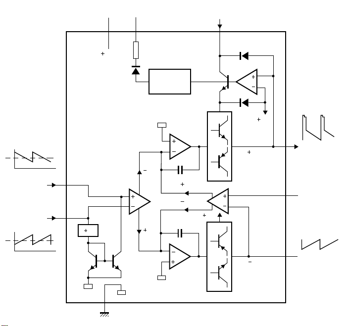
V
V
O(guard)
P
V
FB
36
V
P
TDA8351
I
drive(pos)
I
drive(neg)
1
2
V
5
GND
8
CURRENT
I
S
I
S
SOURCE
V
P
7
V
V
O(A)
I
T
I
T
V
P
V
O(B)
MBC988- 1
O(A)
9
V
I(fb)
4
V
O(B)
Page 47
PINNING
SYMBOL PIN DESCRIPTION
I
drive(pos)
I
drive(neg)
V
P
V
O(B)
1 input power-stage (positive);
includes I
signal bias
I(sb)
2 input power-stage (negative);
includes I
signal bias
I(sb)
3 operating supply voltage
4 output voltage B
GND 5 ground
V
FB
V
O(A)
V
O(guard)
V
I(fb)
handbook, 2 columns
I
drive(pos)
I
drive(neg)
6 input flyback supply voltage
7 output voltage A
8 guard output voltage
9 input feedback voltage
1
2
V
3
P
V
O(B)
4
GND
V
V
O(A)
V
O(guard)
V
FB
I(fb)
5
6
7
8
9
TDA8351
MBC989
Page 48
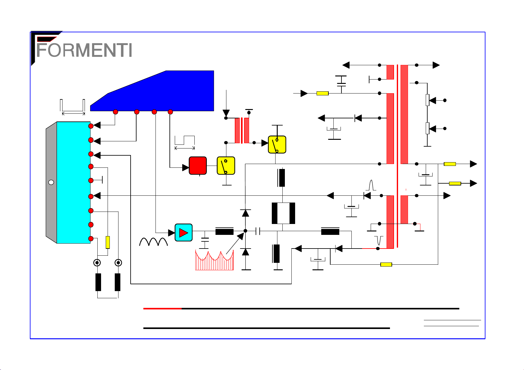
47 46 45 40
20 mS
1
2
3
4
5
6
7
IC 5 TDA8351
8
9
IC 204
TDA8844
64 /uS
EF
TR207
TR12
BUK474
2
TR15
L20
28 V
T 2
D24
D25
4
3
C71
L25
L22
146 V
SUPPLAY
LINE
TR18
BU508D
LINEARITY
YOKE
16 V
PIN 3
TDA8351
HEATER
VOLTAGE
200 VVIDEO
PIN6
TDA8351
L26
C51
50 V
C52
D 53
12
11
9
3
6
T 3
EHT
1
FOCUS
VG2
PIN22
PIN 50
SERVICE
FLYBACK
PULSE TO:
PIP
TUNING
OSD SYNC
B.C.L.
TDA8844
EHT P.
10
C154
7
5
R35
8
5
VERTICAL
YOKE
F19 VERTICAL & LINE OUTPUT
PLUS E-W CORRECTION
F19 V&HDF.DRW
E.G. 27/12/99
Page 49

Page 50
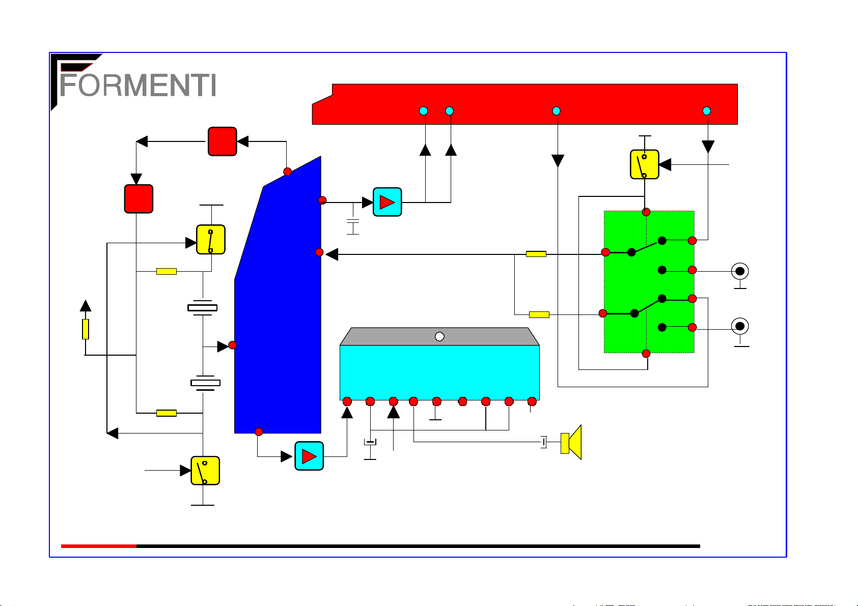
SCART 1
8 V
R208
EF
TR202
R239
F575
IF IN
F576
R242
EF
TR201
TR210
CVBS & INTERCARRIER OUT
6
55
SCART
OUT
EXT. IN
2
IC 204
TDA844X
1SOUND
15
1 3
TR525
IC 400 TDA2613
9 8 7 6 5 4 3 2 1
6 2
TR110
10
2
15
1
12
14
13
11
IC200 (2/3) HEF 4053
FROM PIN8
IC 100
SCART/CINCH
SWITCH
AUDIO
CINCH IN
FROM PIN 12
IC100
SAA5297A
AUDIO OUT
TR575
28 V
TR209
F19 AUDIO MONO SIGNAL PATH
F19AMSPH.DRW
E.G. 29/12799
Page 51

TDA 9870A & TDA9875A MAIN CHARACTERISTICS
FEATURES
Demodulator and decoder section
• Sound IF (SIF) input switch e.g. to select between terrestrial TV SIF and SAT SIF
sources SIF AGC with 24 dB control range SIF 8-bit Analog-to-Digital Converter
(ADC)
• DQPSK demodulation for different standards, simultaneously with 1-channel FM
demodulation NICAM decoding (B/G, I and L standard) Two-carrier
multistandard FM demodulation (B/G, D/K and M standard
• Decoding for three analog multi-channel systems (A2, A2+ and A2*) and satellite
sound Optional AM demodulation for system L, simultaneously with NICAM
• Programmable identification (B/G, D/K and M standard) and different identification
times.
• DSP section
• Digital crossbar switch for all digital signal sources and destinations
• Control of volume, balance, contour, bass, treble,
• pseudo stereo, spatial, bass boost and soft-mute
• Plop-free volume control
• Automatic Volume Level (AVL) control
• Adaptive de-emphasis for satellite
• Programmable beeper
• Monitor selection for FM/AM DC values and signals, with peak detection option I 2 S-bus
interface for a feature extension (e.g. Dolby surround) with matrix, level adjust and
mute.
• Analog audio section
• Analog crossbar switch with inputs for mono and stereo
E.G.Data creazione 01/11/99 17.27 23 / 30 F19MANU.doc
Page 52

• (also applicable as SCART 3 input), SCART 1
• input/output, SCART 2 input/output and line output
• User defined full-level/3 dB scaling for SCART outputs
• Output selection of mono, stereo, dual A/B, dual A or Dual B
• 20 kHz bandwidth for SCART-to-SCART copies
• Standby mode with functionality for SCART copies
• Dual audio digital-to-analog converter from DSP to analog crossbar switch, bandwidth
15 kHz Dual audio ADC from analog inputs to DSP Two dual audio Digital-toAnalog Converters (DACs) for loudspeaker (Main) and headphone (Auxiliary) outputs;
also applicable for L, R, C and S in the Dolby Pro Logic mode with feature extension.
GENERAL DESCRIPTION
The TDA9875A is a single-chip Digital TV Sound Processor (DTVSP) for analog and
digital multi-channel sound systems in TV sets and satellite receivers.
Supported standards
The multistandard/multi-stereo capability of the TDA9875A is mainly of interest in Europe,
but also in Hong Kong/Peoples Republic of China and South East Asia. This includes
B/G, D/K, I, M and L standard. In other application areas there exists only subsets of those
standard combinations otherwise only single standards are transmitted.
M standard is transmitted in Europe by the American Forces Network (AFN) with European
channel spacing (7 MHz VHF, 8 MHz UHF) and monaural sound. The AM sound of L/L’ standard
is normally demodulated in the 1st sound IF. The resulting AF signal has to be entered into the
mono audio input of the TDA9875A. A second possibility is to use the internal AM demodulator
stage, however this gives limited performance. Korea has a stereo sound system similar to Europe
and is supported by the TDA9875A. Differences include deviation, modulation contents and
identification. It is based on M standard.
FUNCTIONAL DESCRIPTION
Description of the demodulator and decoder section
SIF INPUT
E.G.Data creazione 01/11/99 17.27 24 / 30 F19MANU.doc
Page 53

Two input pins are provided, SIF1 e.g. for terrestrial TV and SIF2 e.g. for a satellite tuner.
For higher SIF signal levels the SIF input can be attenuated with an internal switchable
10 dB resistor divider. As no specific filters are integrated, both inputs have the same
specification giving flexibility in application. The selected signal is passed through an AGC
circuit and then digitized by an 8-bit ADC operating at 24.576 MHz.
AGC
The gain of the AGC amplifier is controlled from the ADC output by means of a digital
control loop employing hysteresis. The AGC has a fast attack behaviour to prevent ADC
overloads and a slow decay behaviour to prevent AGC oscillations. For AM demodulation
the AGC must be switched off. When switched off, the control loop is reset and fixed gain
settings can be chosen from Table 15 (subaddress 0).
MIXER
The digitized input signal is fed to the mixers, which mix one or both input sound carriers
down to zero IF. A 24-bit control word for each carrier sets the required frequency. Access
to the mixer control word registers is via the I 2 C-bus. When receiving NICAM programs,
a feedback signal is added to the control word of the second carrier mixer to establish a
carrier-frequency loop.
FM AND AM DEMODULATION
An FM or AM input signal is fed via a band-limiting filter to a demodulator that can be used
for either FM or AM demodulation. Apart from the standard (fixed) de-emphasis
characteristic, an adaptive de-emphasis is available for encoded satellite programs. A
stereo decoder recovers the left and right signal channels from the demodulated sound
carriers. Both the European and Korean stereo systems are supported.
FM IDENTIFICATION
The identification of the FM sound mode is performed by AM synchronous demodulation of
the pilot signal and narrow-band detection of the identification frequencies. The result is
available via the I 2 C-bus interface. A selection can be made via the I 2 C-bus for B/G,
D/K and M standard and for three different modes that represent different trade-offs
between speed and reliability of identification.
NICAM DEMODULATION
The NICAM signal is transmitted in a DQPSK code at a bit rate of 728 kbit/s. The NICAM
demodulator performs DQPSK demodulation and feeds the resulting bitstream and clock
signal onto the NICAM decoder and, for evaluation purposes, to PCLK (pin 1) and NICAM
E.G.Data creazione 01/11/99 17.27 25 / 30 F19MANU.doc
Page 54

(pin 2). A timing loop controls the frequency of the crystal oscillator to lock the sampling
rate to the symbol timing of the NICAM data.
NICAM DECODER
The device performs all decoding functions in accordance with the “EBU NICAM 728
specification”. After locking to the frame alignment word, the data is descrambled by
applying the defined pseudo-random binary sequence; the device will then synchronize to
the periodic frame flag bit C0.
The status of the NICAM decoder can be read out from the NICAM status register by the
user. The OSB bit indicates that the decoder has locked to the NICAM data. The VDSP bit
indicates that the decoder has locked to the NICAM data and that the data is valid sound
data. The C4 bit indicates that the sound conveyed by the FM mono channel is identical to
the sound conveyed by the NICAM channel. The error byte contains the number of sound
sample errors, resulting from parity checking, that occurred in the past 128 ms period.
NICAM AUTO-MUTE
This function is enabled by setting bit AMUTE LOW subaddress 14 Upper and lower error
limits may be defined by writing appropriate values to two registers in the I 2 C-bus section
(subaddresses 16 and 17; . When the number of errors in a 128 ms period exceeds the
upper error limit the auto-mute function will switch the output sound from NICAM to
whatever sound is on the first sound carrier (FM or AM). When the error count is smaller
than the lower error limit the NICAM sound is restored. The auto-mute function can be
disabled by setting bit AMUTE HIGH. In this condition clicks become audible when the
error count increases; the user will hear a signal of degrading quality.
A decision to enable/disable the auto-muting is taken by the microcontroller based on an
interpretation of the application control bits C1, C2, C3 and C4 and, possibly, any
additional strategy implemented by the set maker in the microcontroller software.
For NICAM L applications, it is recommended to demodulate AM sound in the first sound
IF and connect the audio signal to the mono input of the TDA9875A. By setting the AMSEL
bit subaddress 14. the auto-mute function will switch to the audio ADC instead of switching
to the first sound carrier.
CRYSTAL OSCILLATOR
The digital-controlled crystal oscillator (DCXO) is illustrated in Fig.8 (see Chapter 12). The
circuitry of the DCXO is fully integrated, only the external 24.576 MHz crystal is needed.
E.G.Data creazione 01/11/99 17.27 26 / 30 F19MANU.doc
Page 55

TEST PINS
Both test pins are active HIGH, in normal operation of the device they are wired to VSSD1
Test functions are for manufacturing tests only and are not available to customers. Without
external circuitry these pads are pulled down to LOW level with internal resistors.
POWER FAIL DETECTOR
The power fail detector monitors the internal power supply for the digital part of the device.
If the supply has temporary been lower than the specified lower limit, the power-on reset
bit POR, transmitter register subaddress 0 will be set to HIGH. The CLRPOR bit, slave
register subaddress 1 resets the power-on reset flip-flop to LOW. If this is detected, an
initialization of the TDA9875A has to be carried out to ensure reliable operation.
LEVEL SCALING
All input channels to the digital crossbar switch (except for the loudspeaker feedback path)
are equipped with a level adjust facility to change the signal level in a range of 15 dB. It
is recommended to scale all input channels to be 15 dB below full scale (15 dB full scale)
under nominal conditions.
NICAM PATH
The NICAM path has a switchable J17 de-emphasis.
FM (AM) PATH
A high-pass filter suppresses DC offsets from the FM demodulator due to carrier frequency
offsets and supplies the monitor/peak function with DC values and an unfiltered signal, e.g.
for the purpose of carrier detection. The de-emphasis function offers fixed settings for the
supported standards (50 µs, 60 µs 75 µs and J17). An adaptive de-emphasis is available
for Wegener-Panda 1 encoded programs. A matrix performs the dematrixing of the A2
stereo, dual and mono signals.
NICAM AUTO-MUTE
If NICAM B/G, I, D/K is received, the auto-mute is enabled and the signal quality becomes
poor, the digital crossbar switch switches automatically to FM and switches the matrix to
channel 1. The automatic switching depends on the NICAM bit error rate.
The auto-mute function can be disabled via the I 2 C-bus. For NICAM L applications, it is
recommended to demodulate AM sound in the first sound IF and connect the audio signal
to the mono input of the TDA9875A. By setting the AMSEL bit subaddress 14 (see Section
10.3.11), the auto-mute function will switch to the audio ADC instead of switching to the
E.G.Data creazione 01/11/99 17.27 27 / 30 F19MANU.doc
Page 56

first sound carrier. The ADC source selector subaddress 23 (see Section 10.3.20) should
be set to mono input, where the AM sound signal should be connected.
LOUDSPEAKER (MAIN) CHANNEL
The matrix provides the following functions; forced mono, stereo, channel swap, channel
1, channel 2 and spatial effects.
There are fixed coefficient sets for spatial settings of 30%, 40% and 52%.
The Automatic Volume Level (AVL) function provides a constant output level of 23 dB full
scale for input levels between 0 and 29 dB full scale. There are some fixed decay time
constants to choose from, i.e. 2, 4 and 8 seconds.
Pseudo stereo is based on a phase shift in one channel via a 2nd-order all-pass filter.
There are fixed coefficient sets to provide 90 degrees phase shift at frequencies of 150,
200 and 300 Hz.
Volume is controlled individually for each channel ranging from +24 to -83 dB with 1 dB
resolution. There is also a mute position. For the purpose of a simple control software in
the microcontroller, the decimal number that is sent as an I 2 C-bus data byte for volume
control is identical to the volume setting in dBs (e.g. the I 2 C-bus data byte +10 sets the
new volume value to +10 dB).
Balance can be realized by independent control of the left and right channel volume
settings.
Contour is adjustable between 0 and +18 dB with 1 dB resolution. This function is linked to
the volume setting by means of microcontroller software.
Bass is adjustable between +15 and -12 dB with 1 dB resolution and treble is adjustable
between +/-12 dB with 1 dB resolution.
For the purpose of a simple control software in the microcontroller, the decimal number
that is sent as an I 2 C-bus data byte for contour, bass or treble is identical to the new
contour, bass or treble setting in dBs (e.g. the I 2 C-bus data byte +8 sets the new value to
+8 dB). Extra bass boost is provided up to 20 dB with 2 dB resolution. The implemented
coefficient set serves merely as an example on how to use this filter.
The beeper provides tones in a range from approximately 400 Hz to 30 kHz. The
frequency can be selected via the I 2 C-bus. The beeper output signal is added to
theloudspeaker and headphone channel signals. The beeper volume is adjustable with
E.G.Data creazione 01/11/99 17.27 28 / 30 F19MANU.doc
Page 57

respect to full scale between 0 and 93 dB with 3 dB resolution. The beeper is not
effected by mute.
Soft-mute provides a mute ability in addition to volume control with a well defined time (32
ms) after which the soft-mute is completed. A smooth fading is achieved by a cosine
masking.
HEADPHONE (AUXILIARY) CHANNEL
The matrix provides the following functions; forced mono, stereo, channel swap, channel
and channel 2 (or C and S in Dolby Surround Pro Logic mode). Volume is controlled
individually for each channel in a range from +24 to 83 dB with 1 dB resolution. There is
also a mute position. For the purpose of a simple control software in the microcontroller,
the decimal number that is sent as an I 2 C-bus data byte for volume control is identical to
the volume setting in dB (e.g. the I 2 C-bus data byte +10 sets the new volume value to
+10 dB). Balance can be realized by independent control of the left and right channel
volume settings.
Bass is adjustable between +15 and -12 dB with 1 dB resolution and treble is adjustable
between +/- 12 dB with 1 dB resolution.
For the purpose of a simple control software in the microcontroller, the decimal number
that is sent as an I 2 C-bus data byte for bass or treble is identical to the new bass or
treble setting in dB (e.g. the I 2 C-bus data byte +8 sets the new value to +8 dB).
The beeper provides tones in a range from approximately 400 Hz to 30 kHz. The
frequency can be selected via the I 2 C-bus. The beeper output signal is added to the
loudspeaker and headphone channel signals. The beeper volume is adjustable with
respect to full scale between 0 and 93 dB with 3 dB resolution. The beeper is not
effected by mute.
Soft-mute provides a mute ability in addition to volume control with a well defined time (32
ms) after which the soft-mute is completed. A smooth fading is achieved by a cosine
masking.
SCART INPUTS
The SCART specification allows for a signal level of up to 2 V (rms). Because of signal
handling limitations, due to the 5 V supply voltage of the TDA9875A, it is necessary to
have fixed 3 dB attenuators at the SCART inputs to obtain a 2 V input. This results in a +3
dB SCART-to-SCART copy gain. If 0 dB copy gain is preferred (with maximum 1.4V input),
there are +3 dB/0 dB amplifiers at the outputs of SCART 1 and SCART 2 and at the line
E.G.Data creazione 01/11/99 17.27 29 / 30 F19MANU.doc
Page 58

output. The input attenuator is realized by an external series resistor in combination with
the input impedance, both of which form a voltage divider. With this voltage divider the
maximum SCART signal level of 2 V (rms) is scaled down to 1.4 V (rms) at the input pin.
EXTERNAL AND MONO INPUTS
The 3 dB input attenuators are not required for the external and mono inputs, because
those signal levels are under control of the TV designer. The maximum allowed input level
is 1.4 V (rms). By adding external series resistors, the external inputs can be used as an
additional SCART input.
SCART OUTPUTS
The SCART outputs employ amplifiers with two gain settings. The gain can be set to +3
dB or to 0 dB via the I 2 C-bus. The +3 dB position is needed to compensate for the 3 dB
attenuation at the SCART inputs should SCART-to-SCART copies with 0 dB gain be
preferred [under the condition of 1.4 V (rms) maximum input level]. The 0 dB position is
needed, for example, for an external-to-SCART copy with 0 dB gain.
LINE OUTPUT
The line output can provide an unprocessed copy of the audio signal in the loudspeaker
channels. This can be either an external signal that comes from the dual audio ADC, or a
signal from an internal digital audio source that comes from the dual audio DAC. The line
output employs amplifiers with two gain settings. The +3 dB position is needed to
compensate for the attenuation at the SCART inputs, while the 0 dB position is needed, for
example, for non-attenuated external or internal digital signals (see Section 6.3.4).
E.G.Data creazione 01/11/99 17.27 30 / 30 F19MANU.doc
Page 59
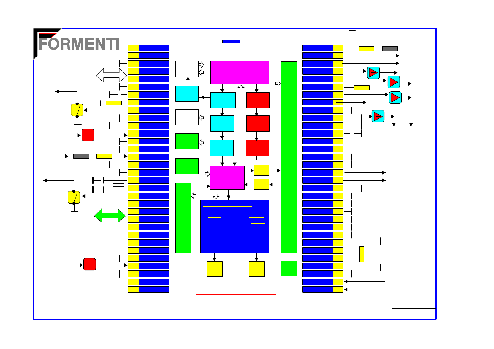
TO PIN 9 IC1
TDA9811
TR8
INTERCARRIER
FROM PIN 20 IC1
TDA9811
6 V
TO L/L' FILTER
SWITCH
TR8
AM AUDIO
FROM PIN 22 IC1
TDA9811
STD SWITCH
EF
L /L' SWITCH
II S
TR6
EF
IIC BUS
1
2
3
4
5
6
7
8
9
10
11
12
13
14
15
16
CRESET
17
18
19
20
21
SYSLCK
22
23
24
25
26
27
28
29
MONOIN
30
31
32
PLCK
NICAM
ADDR1
SCL
SDA
VSSA1
VDEC1
Iref
P1
SIF2
Vref
SIF1
ADDR2
Vssd1
Vdd1
Vssd4
XTAL1
XTAL0
P2
SCK
WS
SDO2
SDO1
SDI2
SDI1
TEST1
TEST2
EXT/R
EXT/L
IIC
IN / OUT
IDENT
I / O
PORT
PEAK
DETEC.
VCXO
CLOCK
IIS
ENC.
DEC.
INPUT SWITCH
AGC ADC
FM DEM
(AM DEM)
DEMATR
DEEMPH
LEVEL
ADJ.
CHANNEL
SELECTION
QPSK
DEM.
NICAM
DEC.
LEVEL
ADJ.
DAC
DAC
AUDIO PROCESSING
L.S.
AVL,VOL
CONTOUR
BASS
TREBLE
PSEUDO
BASS CORR
DAC DAC
H.P.
VOL.
BASS
TREB.
TDA9875A
VDD2
LOR
LOL
MOL
MOR
ANALOGUE CROSS BAR SWITCH
Vdda
AUXOL
AUXOR
Vssa3
pcapl
pcapr
vREF3
SCOL2
SCOR2
Vssa4
Vssd2
SCOL1
SCOR2
Vref2
i.c.
i.c.
Vssa2
i.c.
i.c.
Vref(n)
Vref(p)
Vdec2
SCIL2
TEST
SCIR2
Vssd3
SCIL1
SCIR1
64
63
AUDIO LINE OUT
62
61
60
59
58
57
56
55
54
53
52
51
50
49
48
AUDIO OUT TO SCART
47
46
45
44
43
42
41
40
39
38
37
36
35
34
AUDIO FROM SCART
33
TR9
6 V
TR11
TR12
TO HEADPHONES
APLIFIER
IC4
TDA2822M
6 V
TO AUDIO
AMPLIFIER
TR10
TDA9875A PINOUT & PERIPHERALS
TDA9875A.DRW
E.G. 7/11/99
Page 60

TDA9811
Multistandard VIF-PLL
with QSS-IF and AM demodulator
FEATURES
• 5 V supply voltage
• Two switched VIF inputs, gain controlled wide band VIF-amplifier (AC-coupled)
• True synchronous demodulation with active carrier regeneration (very linear
demodulation, good intermodulation figures, reduced harmonics, excellent pulse
response)
• Gated phase detector for L/L accent standard VCO frequency switchable between L
and L accent (alignment external) picture carrier frequency
• Separate video amplifier for sound trap buffering with high video bandwidth VIF AGC
detector for gain control, operating as peak sync detector for B/G (optional external
AGC) and peak white detector for L; signal controlled reaction time for L
• Tuner AGC with adjustable takeover point (TOP)
• AFC detector without extra reference circuit
• SIF input for single reference QSS mode (PLL controlled); SIF AGC detector for gain
controlled SIF amplifier; single reference QSS mixer able to operate in high
performance single reference QSS mode
• AM demodulator without extra reference circuit
• AM mute (especially for NICAM)
• Stabilizer circuit for ripple rejection and to achieve constant output signals.
GENERAL DESCRIPTION
The TDA9811 is an integrated circuit for multistandard vision IF signal processing and
sound AM demodulation, with single reference QSS-IF in TV and VCR sets.
TDA9811 QSS Pagina 1 di 4 e.g. TDA9811R
Page 61
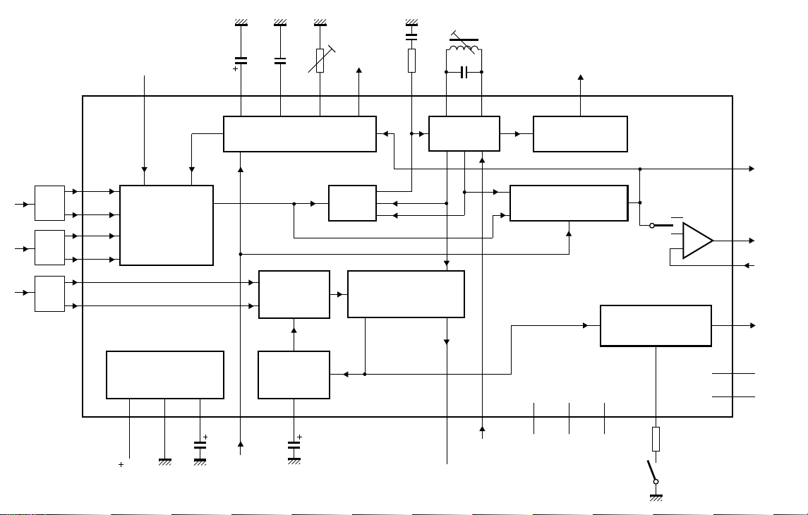
VIF input switch
C
AGCCBL
TOP
tuner
AGC
loop
filter
2 x f
PC
AFC
2324257192830 63
VIFB
VIFA
SIF
5
4
VIF AMPLIFIER
2
INPUT SWITCH
1
32
31
INTERNAL VOLTAGE
STABILIZER
29 27 26 9 8
5 V
AND
TUNER AND VIF-AGC
AMPLIFIER
SIF-AGC
VP1/2
standard
switch
SIF
C
AGC
FPLL
SINGLE REFERENCE
MIXER AND
AM DEMODULATOR
VCO TWD
20
(2nd SIF)
V
o QSS
L′/L
switch
AFC DETECTOR
VIDEO DEMODULATOR
AND AMPLIFIER
TDA9811
1811
n.c.16n.c.15n.c.
VIDEO
BUFFER
AF AMPLIFIER
AND SWITCH
17
mute switch, AM
21
video
1 V (p-p)
10
22
12
13
14
CVBS
2 V (p-p)
V
i(vid)
AF/AM
n.c.
n.c.
MHA046
Page 62

FUNCTIONAL DESCRIPTION
Vision IF amplifier and input switch The vision IF amplifier consists of three AC-coupled
differential amplifier stages. Each differential stage comprises a feedback network
controlled by emitterdegeneration. T
The first differential stage is extended by two pairs of emitter followers to provide two IF
input channels. The VIF input can be selected by pin 30
Tuner and VIF AGC
The AGC capacitor voltage is transferred to an internal IF control signal, and is fed to the
tuner AGC to generate the tuner AGC output current (open-collector output).
The tuner AGC takeover point can be adjusted. This allows the tuner and the SWIF filter to
be matched to achieve the optimum IF input level.
The AGC detector charges/discharges the AGC capacitorto the required voltage for setting
of VIF and tuner gain in order to keep the video signal at a constant level.
Therefore for negative video modulation the sync level and for positive video modulation
the peak white level of the video signal is detected. In order to reduce the reaction
time for positive modulation, where a very large time constant is needed, an additional
level detector increases the discharging current of the AGC capacitor (fast mode)
in the event of a decreasing VIF amplitude step. The additional level information is given
by the black-level detector voltage.
Frequency Phase Locked Loop detector (FPLL)
The VIF-amplifier output signal is fed into a frequency detector and into a phase detector
via a limiting amplifier.
During acquisition the frequency detector produces a DC current proportional to the
frequency difference between the input and the VCO signal. After frequency lock-in the
phase detector produces a DC current proportional to the phase difference between the
VCO and the input signal. The DC current of either frequency detector or phase detector is
converted into a DC voltage via the loop filter, which controls the VCO frequency. In the
event of positive modulated signals the phase detector is gated by composite sync in order
to avoid signal distortion for overmodulated VIF signals.
TDA9811 QSS Pagina 2 di 4 e.g. TDA9811R
Page 63

VCO, Travelling Wave Divider (TWD) and AFC
The VCO operates with a resonance circuit (with L and C in parallel) at double the PC
frequency. The VCO is controlled by two integrated variable capacitors.
The control voltage required to tune the VCO from its free-running frequency to actually
double the PC frequency is generated by the frequency-phase detector and fed via the
loop filter to the first variable capacitor (FPLL). This control voltage is amplified and
additionally converted into a current which represents the AFC output signal. The VCO
centre frequency can be decreased (required for L accent standard) by activating an
additional internal capacitor. This is achieved by using the L accent switch. In this event
the second variable capacitor can be controlled by a variable resistor at the L accent
switch for setting the VCO centre frequency to the required L accent value. At centre
frequency the AFC output current is equal to zero.
The oscillator signal is divided-by-two with a TWD which generates two differential output
signals with a 90 degree phase difference independent of the frequency.
Video demodulator and amplifier
The video demodulator is realized by a multiplier which is designed for low distortion and
large bandwidth. The vision IF input signal is multiplied with the ‘in phase’ signal of the
travelling wave divider output. In the demodulator stage the video signal polarity can be
switched in accordancewith the TV standard. The demodulator output signal is fed via an
integrated low-pass filter for attenuation of the carrier harmonics to the video amplifier. The
video amplifier is realized by an operational amplifier with internal feedback and high
bandwidth. A low-pass filter is integrated to achieve an attenuation of the carrier harmonics
for B/G and L standard. The standard dependent level shift in this stage delivers the same
sync level for positive and negative modulation. The video output signal is 1 V (p-p) for
nominal vision IF modulation.
Video buffer
For an easy adaption of the sound traps an operational amplifier with internal feedback is
used in the event of B/G and L standard. This amplifier is featured with a high bandwidth
and 7 dB gain. The input impedance is adapted output stage delivers a nominal 2 V (p-p)
positive video signal. Noise clipping is provided.
TDA9811 QSS Pagina 3 di 4 e.g. TDA9811R
Page 64

SIF amplifier and AGC
The sound IF amplifier consists of two AC-coupled differential amplifier stages. Each
differential stage comprises a controlled feedback network provided by emitter
degeneration. The SIF AGC detector is related to the SIF input signals (average level of
AM or FM carriers) and controls the SIF amplifier to provide a constant SIF signal to the
AM demodulator and single reference QSS mixer. The SIF AGC reaction time is set to
‘slow’ for nominal video conditions. But with a decreasing VIF amplitude step the SIF AGC
is set to ‘fast’ mode controlled by the VIF AGC detector. In FM mode this reaction time is
also set to ‘fast’ controlled by the standard switch.
Single reference QSS mixer The single reference QSS mixer is realized by a multiplier.
The SIF amplifier output signal is fed to the single reference QSS mixer and converted to
intercarrier frequency by the regenerated picture carrier (VCO).
The mixer output signal is fed via a high-pass for attenuation of the video signal
components to the output pin 20. With this system a high performance hi-fi stereo
sound processing can be achieved.
AM demodulator
The AM demodulator is realized by a multiplier. The modulated SIF amplifier output signal
is multiplied in phase with the limited (AM is removed) SIF amplifier output signal. The
demodulator output signal is fed via an integrated low-pass filter for attenuation of the
carrier harmonics to the AF amplifier.
Internal voltage stabilizer and 1 ¤2 VP -reference
The bandgap circuit internally generates a voltage of approximately 1.25 V, independent of
supply voltage and temperature. A voltage regulator circuit, connected to this voltage,
produces a constant voltage of 3.6 V which is used as an internal reference voltage.
For all audio output signals the constant reference voltage cannot be used because large
output signals are required.
TDA9811 QSS Pagina 4 di 4 e.g. TDA9811R
Page 65
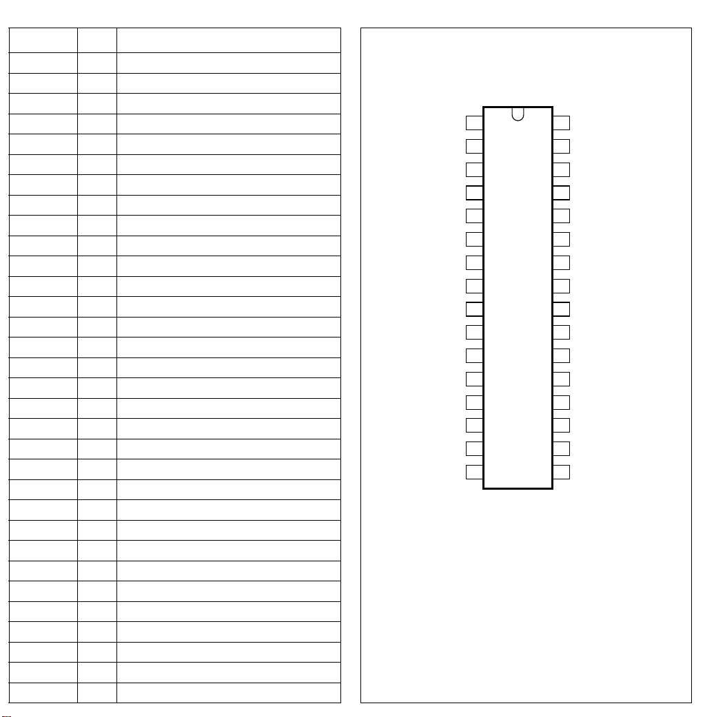
PINNING
SYMBOL PIN DESCRIPTION
V
V
C
V
V
i VIF1
i VIF2
BL
i VIF3
i VIF4
1 VIF differential input signal voltage 1
2 VIF differential input signal voltage 2
3 black level detector
4 VIF differential input signal voltage 3
5 VIF differential input signal voltage 4
TADJ 6 tuner AGC takeover adjust (TOP)
T
PLL
C
SAGC
7 PLL loop filter
8 SIF AGC capacitor
STD 9 standard switch
V
o CVBS
10 CVBS output signal voltage
LSWI 11 L/L accent switch
V
oAF
12 AM audio voltage frequency output
n.c. 13 not connected
n.c. 14 not connected
n.c. 15 not connected
n.c. 16 not connected
MUTE 17 AM mute
n.c. 18 not connected
TAGC 19 tuner AGC output
V
o QSS
V
o(vid)
V
i(vid)
20 single reference QSS output voltage
21 composite video output voltage
22 video buffer input voltage
AFC 23 AFC output
VCO1 24 VCO1 reference circuit for 2f
VCO2 25 VCO2 reference circuit for 2f
C
ref
261⁄2VP reference capacitor
PC
PC
GND 27 ground
C
V
VAGC
P
28 VIF AGC capacitor
29 supply voltage
INSWI 30 VIF input switch
V
V
i SIF1
i SIF2
31 SIF differential input signal voltage 1
32 SIF differential input signal voltage 2
ndbook, halfpage
V
V
V
V
C
V
o CVBS
i VIF1
i VIF2
C
BL
i VIF3
i VIF4
TADJ
T
PLL
SAGC
STD
LSWI
V
o AF
n.c.
n.c.
n.c.
n.c.
1
2
3
4
5
6
7
8
9
10
11
12
13
14
15
16
TDA9811
Fig.2 Pin configuration.
MHA047
V
32
i SIF2
V
31
i SIF1
30
INSWI
V
29
P
C
28
VAGC
GND
27
C
26
ref
VCO2
25
VCO1
24
AFC
23
V
22
i(vid)
V
21
o(vid)
V
20
o QSS
TAGC
19
18
n.c.
17
MUTE
Page 66

TDA9830
TV sound AM-demodulator and
audio source switch
FEATURES
• Adjustment free wideband synchronous AM demodulator
• Audio source-mute switch (low noise)
• Audio level according EN50049
• 5 to 8 V power supply or 12 V alternative
• Low power consumption.
GENERAL DESCRIPTION
The TDA9830, a monolithic integrated circuit, is designed for AM-sound demodulation
used in L- and L’-standard.
The IC provides an audio source selector and also mute switch.
FUNCTIONAL DESCRIPTION
Sound IF input
The sound IF amplifier consists of three AC-coupled differential amplifier stages each with
approximately 20 dB gain. At the output of each stage is a multiplier for gain controlling
(→ current distribution gain control). The overall control range is approximately -6 to +60
dB and the frequency response (-3 dB) of the IF amplifier is approximately 6 to 70 MHz.
The steepness of gain control is approximately 10 mV/dB.
IF AGC
The automatic gain control voltage to maintain the AM demodulator output signal at a
constant level is generated by a mean level detector. This AGC-detector charges and
discharges the capacitor at pin 3 controlled by the output signal of the AM-demodulator
compared to an internal reference voltage. The maximum charge/discharge current is
approximately 5 mA. This value in combination with the value of the AGC capacitor and
the AGC steepness determines the lower cut-off audio frequency and the THD-figure at
low modulation frequency of the whole AM-demodulator. Therefore a large time constant
has to be chosen which leads to slow AGC reaction at IF level change. To speed up the
AGC in case of IF signal jump from low to high level, there is an additional comparator built
in, which can provide additional discharge current from the AGC capacitor up to 5 mA in a
case of overloading the AM demodulator by the internal IF signal.
AM-demodulator
The IF amplifier output signal is fed to a limiting amplifier (two stages) and to a multiplier
circuit. However the limiter output signal (which is not any more AM modulated) is also fed
to the multiplier, which provides AM demodulation (in phase demodulation). After lowpass
filtering (fg ≈ 400 kHz) for carrier rejection and buffering, the demodulator output signal is
present at pin 6. The AM demodulator operates over a wide frequency range, so that in
Page 67
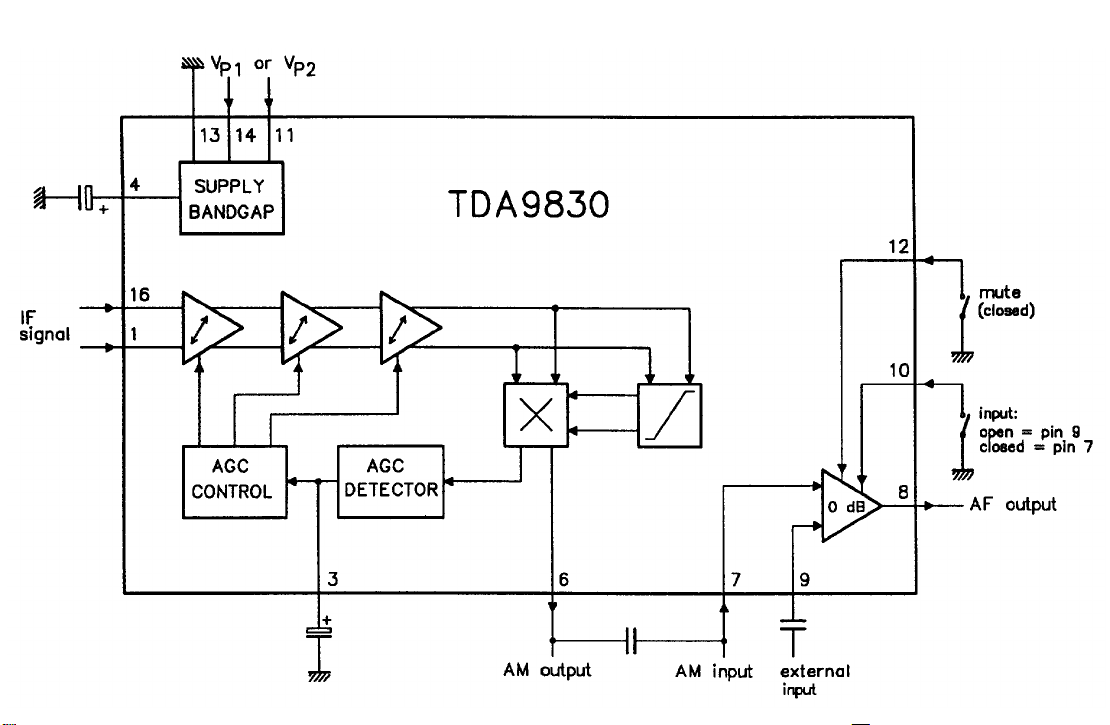
Page 68

combination with the frequency response of the IF amplifier applications in a frequency
range from approximately 6 MHz up to 70 MHz are possible.
Audio switch
This circuit is an operational amplifier with three input stages and internal feedback
network determining gain (0 dB) and frequency response (fg ≈ 700 kHz). Two of the input
stages are connected to pin 7 and pin 9, the third input stage to an internal reference
voltage. Controlled by the switching pins 10 and 12, one of the three input stages can be
activated and a choice made between two different AF signals or mute state. The selected
signal is present at pin 8. The decoupling capacitors at the input pins are needed, because
the internally generated bias voltage for the input stages must not be influenced by the
application in order to avoid DC-plop in case of switching.
The AM demodulator output is designed to provide almost the same DC voltage as the
input bias voltage of the audio switch. But there may be spread between both voltages.
Therefore it is possible to connect pin 6 directly to pin 7 (without a decoupling capacitor),
but in this event the DC-plop for switching can increase up to 100 mV.
Reference circuit
This circuit is a band gap stabilizer in combination with a voltage regulation amplifier,
which provides an internal reference voltage of about 3.6 V nearly independent from
supply voltage and temperature. This reference voltage is filtered by the capacitor at pin 4
in order to reduce noise. It is used as a reference to generate all important voltages and
currents of the circuit. For application in 12 V power supply concepts, there is an internal
voltage divider in combination with a Darlington transistor in order to reduce the supply
voltage for all IC function blocks to approximately 6 V.
This is necessary because of use of modern high frequency IC technology, where most of
the used integrated components are only allowed to operate at maximum 9 V supply
voltage.
Page 69
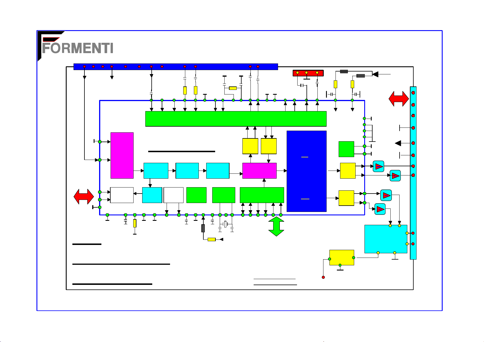
MONO
7 5
12
8 11 96 10
INPUT
A1
6V
29 31
INTERCARRIER INPUT
10
INPUT
IIC
SCL
SDA
12
4
5
3
IIC ADDRES.
6
SWITCH
AGC
ADC
IIC
VSSA1
7 8
TDA9870A
FM DEM
(AM DEM)
IDENT
14 15 16
17
F19
STEREO A2
MODULE
EXT. IN
2 1 4 3
32 33 34
36
37
35
38 39
ANALOGUE CROSS BAR SWITCH
DEMATR
DEEMPH
I / O
PORT
9
20
PEAK
DETECT.
2° IIC ADDRESS
11
LEVEL
ADJ.
VCXO
CLOCK
13
18 19
22 23
21
6 V
SCART OUT
SCART SOUND OUT
47 48
DAC
CHANNEL
SELECTION
IIS
IIS
ENC / DEC.
24 25
F19STA2 .DRV
E.G 5/11/99
LINE OUT
A3
50
49 59 64
51
52
62 63
VDDA3VDDD2
VSSD2
VSSA2
VSSA3
VSSA4
TEST
DAC
DAC
KIA7812
1
2
DAC
26 27
AUDIO
PROCESSING
L.S.
AVL, VOL
CONTOUR, BASS
TREB, PSEU
BASSCORR
BEEPER
H.P.
VOL, BEEP.
BASS, TREB.
IIS
3
IC 5
49
43
56
50
28
30
60
61
57
58
IC 4
6 V
26V
TR10
TR12
TR11
HEADPHONES
AMPLIFIER
TDA2822M
2 4
12 V
TR9
7 6
A2
IIC
1
2
3
4
7
10
8
9
1
5
3
6
Page 70
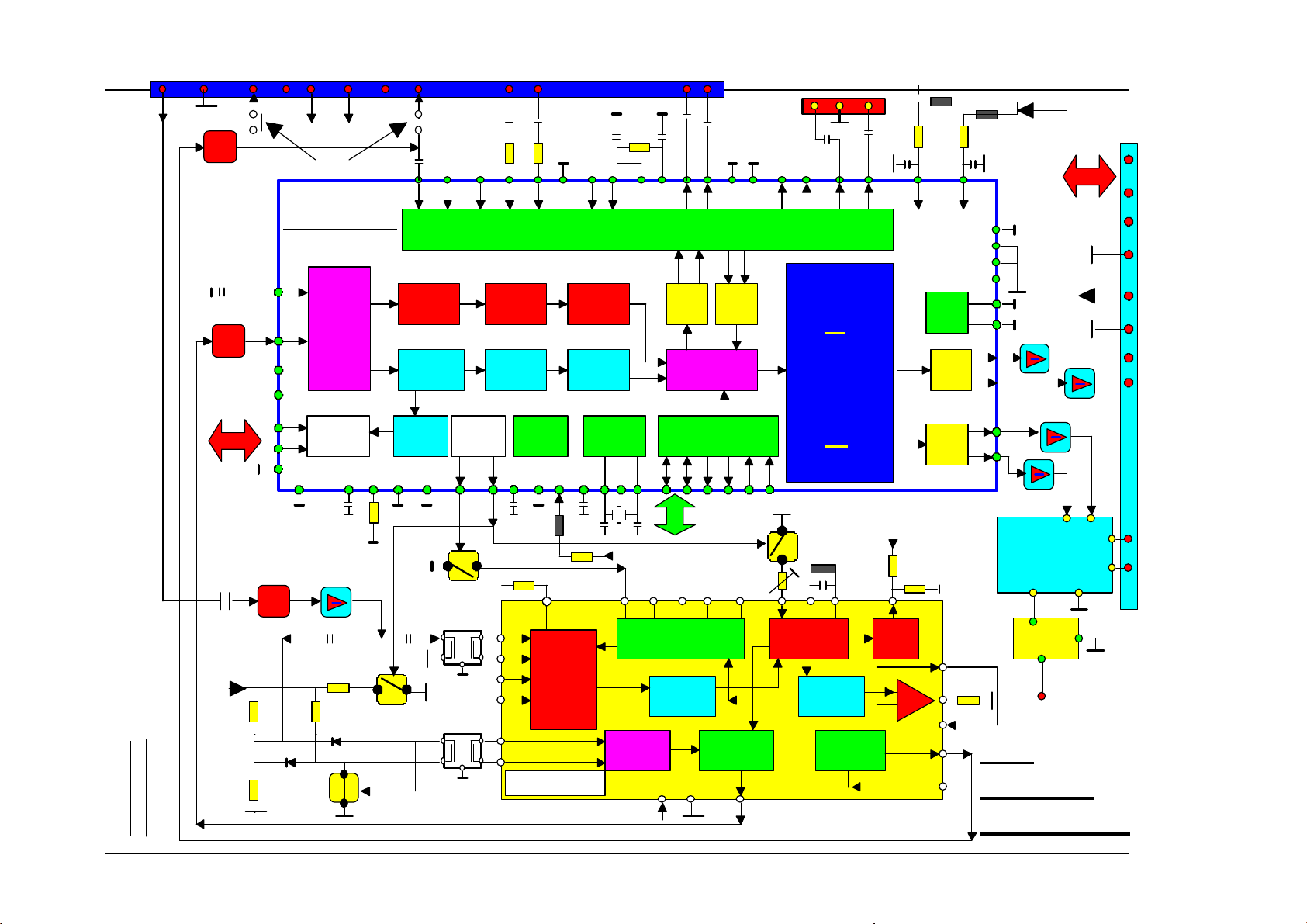
7 5 12 8 11 96 10
2 1 4 3
IF IN
TR6
12 V
F19NICAM.DRV
E.G 5/11/99
EF
TR1
EF
STEREO INTERCARRIER ONLY
SCL
IIC
SDA
TR5
EF
R5
6V
R6
6V 12V
TDA9875A
10
INPUT
SWITCH
12
AGC
ADC
1
PLK
2
NICAM
DATA
4
IIC
5
3
IIC ADDR.
6
D1
7
TR4
R7
R6
D2
TR2
29 31 32 33 34
QPSK
DEM.
FM DEM
(AM DEM)
IDENT
8
L /L'
14 15
17 20
FOS2
TR3
2
1
FOS 1
EXT. IN
36 37
35
38 39
47 48
ANALOGUE CROSS BAR SWITCH
I / O
PORT
3
NICAM
DEC.
DEMATR
DEEMPH
DETECT.
2° IIC ADDRESS
9
11 13
TR8
8V
1
2
4
5
31
32
TDA 9811
IC 1
PEAK
30
VIF SWT.
IF AMPL.
&
VIDEO
SWITCH
LEVEL
ADJ.
LEVEL
ADJ.
VCXO
CLOCK
18 19
16
STD
DAC
CHANNEL
SELECTION
22 23
21
IIS
6 V
28 3 6 19
9
TUNER & VIF AGC
FPLL
SIF
AMPL.
29 27
5 V
IIS
ENC / DEC.
A1
SCART SOUND OUT
49 59 64
A3
50
51 52 62 63
AUDIO
DAC
PROCESSING
L.S.
AVL, VOL
CONTOUR, BASS
TREB, PSEU
BASSCORR
BEEPER
IIS
24 25
L/L'
FM MIXER
& AM DEM.
26 27
R20
11
20
H.P.
VOL, BEEP.
BASS, TREB.
TR7
L1
24 25
VCO AFC
VIDEO
DEMOD.
AF AMPL.
23
& SWT.
VDDA3VDDD2
VSSD2
VSSA2
VSSA3
VSSA4
TEST
DAC
DAC
8 V
21
10
22
12
17
MUTE
6 V
IIC
49
43
56
50
28
30
60
61
57
58
HEADPHONES
IC 4
TR10
TR12
TR11
AMPLIFIER
TDA2822M
2 4
12 V
3
KIA7812
26 V
26V
TR9
7 6
2
1
IC 5
FROM
PIM 7
A2
F19
NICAM
MODULE
A2
1
3
1
2
3
4
7
10
8
9
5
6
Page 71
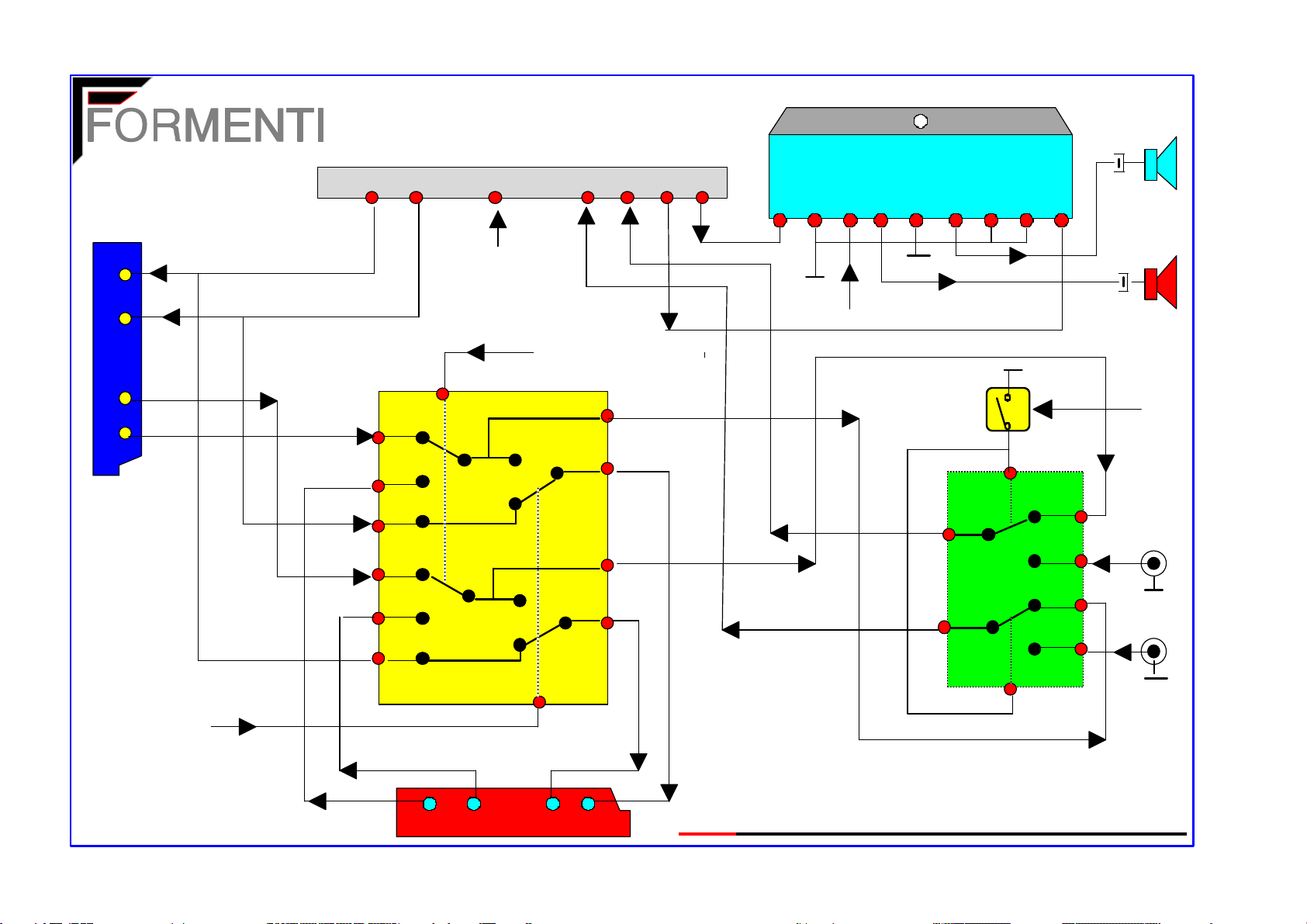
STEREO MODULE CONNECTOR
1 973 4
82
IC 400 TDA1521A
9 8 7 6 5 4 3 2 1
1
3
2
6
SCART 1
19
12
18
17
13
14
FROM PIN 11
TUNER (I.F.)
FROM PIN 6 IC 100
AV1 / AV2
SWITCH
4
FROM PIN8
20
16
11
15
8
TR110
10
15
12
14
13
11
IC 100
SCART/CINCH
SWITCH
2
1
AUDIO
CINCH IN
FROM PIN 7 IC 100
TV/AV SWITCH
TO AV2
F19ASSPH.DRW
E.G. 29/12799
SCART 2
IC201 (2/3 OF LA7955)
6 2 1 3
IC200 (2/3) HEF 4053
F19 AUDIO STEREO SIGNAL PATH
Page 72

Page 73

TDA4605
Control IC for Switched-Mode Power Supplies
using MOS-Transistors
Features
• Fold-back characteristic provides overload protection for external components
• Burst operation under short-circuit conditions
• Loop error protection
• Switch-off if line voltage is too low (undervoltage switch-off)
• Line voltage compensation of overload point
• Soft-start for quiet start-up
• Chip-over temperature protection (thermal shutdown)
• On-chip parasitic transformer oscillation suppression circuitry
Functional desciption
The IC TDA 4605-1 controls the MOS-power transistor and performs all necessary
regulation and monitoring functions in free running flyback converters. Since good load
regulation over a wide load range is attained, this IC is applicable tor consumer and
industrial power supplies.
The serial circuit of power transistor and primary winding of the flyback transformer is
connected to the input voltage. During the switch - on period of the transistor, energy is
stored in the transformer and during the switch - off period it is fed to the load via the
secondary winding. By varying switch-ontime of the power transistor, the IC controls each
portion of energy transferred to the secondary side such that the output voltage remains
nearly independent ot load variations.
The required control information is taken from the input voltage during the switch-on period
and from a regulation winding during the switch-off period.
In the different load ranges the switched-mode power supply (SMPS) behaves as follow:
TDA4605 SMPS CONTRO I.C. Pagina 1 di 6
e.g.tda4605R.doc
Page 74

No load operation:
The power supply unit oscillates at its resonant frequency typ. 100 kHz to 200 kHz.
Depending upon
the transformator windings the output voltage can be slightly above nominal value.
Nominal operation:
The switching frequency declines with increasing load and decreasing AC-voltage. The
duty factor primarly depends on the AC-voltage. The output voltage is load-dependent
only.
Overload point:
Maximal output power is available at this point ot the output characteristic.
Overload:
The energy transferred per operation cycle is limited at the top. Therefore the output
voltage declines by secondary overloading..Semiconductor Group 35
TDA 4605 Pin Definitions and Functions
Pin No. Function
1 Regulating Voltage: Information input concerning secondary voltage. By
comparing the regulating voltage - obtained from the regulating winding ot the transformer
- with the internal reference voltage, the output impulse width on pin 5is adapted to the
load ot the secondary side (normal, overload, short-circuit, no load).
2 Primary Current Simulation: Information input regarding the primary current.
The primary current rise in the primary winding is simulated at pin 2 as a voltagerise by
means ot external RC-element. When a value is reached that is derivedfrom the regulating
voltage at pin 1, the output impulse at pin 5 is terminated. TheRC-element serves to set
the maximum power at the overload point set.
3 Input for Primary Voltage Monitoring: In the normal operation V 3 is moving
between the thresholds V 3H and V 3L (V 3H > V 3 > V 3L ). V 3 < V 3L : SMPS is
switched OFF (line voltage too low). V 3 > V 3H : Compensation of the overload point
regulation (controlled by pin 2) starts at V 3H : V 3L = 1.7.
TDA4605 SMPS CONTRO I.C. Pagina 2 di 6
e.g.tda4605R.doc
Page 75

4 Ground
5 Output: Push-pull-output provides 1 A for rapid charge and discharge of the
gate capacitance ot the power MOS-transistor.
5 Supply Voltage Input: A stable internal reference voltage V REF is derived from
the supply voltage also the switching thresholds V 6A , V 6E , V 6 max and V 6 min for the
supply voltage detector. If V 6 > V 6E then V REF is switched on and swiched off when V
6 < V 6A . In addition the logic is only enable for V 6 min < V 6 < V 6 max .
7 Soft-Start: Input for soft-start. Start-up will begin with short pulses by connecting a
capacitor from pin 7 to ground.
8 Zero Detector: Input tor the oscillation feedback. After starting oscillation, every
zero transit of the feedback voltage (falling edge) triggers an output impulse at
pin 5. The trigger threshold is at + 50 mV typical..Semiconductor Group 36
TDA 4605 Application Circuit
Application circuit shows a flyback converter for video recorders with a power rating of 50
W. The circuit is designed as a wide-range power supply tor AC-line voltages ot 90 to 270
V. The AC-input voltage is rectified by bridge rectifier GR1 and smoothed by C 1 . The
NTC limits the rush in current.In the period before the switch-on threshold is reached the
IC is supplied via resistor R 1 ; during the start-up phase it uses the energy stored in C 2 ,
under steady-state conditions the IC receives its supply voltage from transformer winding n
1 via diode D1. The switching transistor T1 is a BUZ 90.
The parallel-connected capacitor C 3 and the inductance ot primary winding 112 determine
the system resonance frequency. The R 2 - C 4 - D2 circuitry limits overshoot peaks, and
R 3 protects the gate of T1 against static charges.
While T1 conducts, the current rise in the primary winding depends on the winding’s
inductance and the V C1 voltage. A voltage reproduction ot the current rise is tabbed using
the R 4 - C 5 network and forwarded into pin 2 ot the IC. The RC-time constant ot R 4 , R 5
must be dimensioned correctly in order to prevent driving the transformer core into
saturation.
The R 10 /R 11 divider ratio provides the line voltage threshold controlling the
undervoltage control circuit in the IC. The voltage present at pin 3 also determines the
overload. Detection of overload together with the current characteristic at pin 2 controls the
on period ot T1. This keeps the cut-off point stable even with higher AC-line voltages.
TDA4605 SMPS CONTRO I.C. Pagina 3 di 6
e.g.tda4605R.doc
Page 76

Pin 3 The down-divide primary voltage applied there stabilizes the overload point. In
addition the logic is disabled in the event of low voltage by comparison with the internal
stable voltage V V in the primary voltage monitor block.
Pin 4 Ground
Pin 5 In the output stage the output signals produced by the logic are shifted to a leved
suitable for MOS-power transistors.
Pin 6 From the supply voltage V 6 are derived a stable internal reference V REF and the
switching threshold V 6A , V 6E , V 6 max and V 6 min for the supply voltage monitor. All
reference values (V R , V 2B , V ST ) are derived from V REF . If V 6 > V VE the V REF is
switched on and switched off when V 6 < V 6A . In addition, the logic is released only for V
6 min < V 6 < V 6 max .
Pin 7 The output of the overload amplifier is connected to pin 7. A load on this output
causes a reductio in maximal impulse duration. This function can be used to implement a
soft start, when pin 7 is connected to ground by a capacitor
Pin 8 The zero detector controlling the logic block recognizes the transformer being
discharged by positive to negative zero crossing of pin 8 voltage and enables the logic for
a new pulse. Parasitic oscillations occurring at the end of a pulse cannot lead to a new
pulse (double-pulsing), because an internal circuit inhibits the zero detector for a finite time
t UL after the end of each pulse.
Start-Up Behaviour
The start-up behaviour of the application circuit per sheet 48 is represented on sheet 50
for a line voltage barely above the lower acceptable limit voltage value (without soft-start).
After applying the line voltage at the time t 0 to the tollowing voltages built up:
– V 6 corresponding to the half-wave charge current over R 1
– V 2 to V 2 max (typically 6.6 V)
– V 3 to the value determined by the divider R 10 /R 11 .
The current drawn by the IC in this case is less than 1.6 mA. If V 6 reaches the threshold V
6E (time point t 1 ), the IC switches on the internal reference voltage. The currentdraw
max. rises to 12 mA.
The primary current- voltage reproducer regulates V 2 down to V 2E and the starting
impulse generator generates the starting impulses from time point t 5 to t 6 . The feedback
to pin 8 starts the next impulse and so on. All impulses including the starting impulse are
TDA4605 SMPS CONTRO I.C. Pagina 5 di 6
e.g.tda4605R.doc
Page 77

controlled in width by regulating voltage of pin 1. When switching on this corresponds to a
short-circuit event, i.e. V 1 = 0.
Hence the IC starts up with "short-circuit impulses" to assume a width depending on the
regulating voltage feedback (the IC operates in the overload range). The maximum pulse
width is reached at time point t 2 (V 2 = V 2 max ). The IC operates at the overload point.
Thereafter the peak values ot V 2 decrease rapidly, as the IC is operating within the
regulation range. The regulating loop has built up. If voltage V 6 falls below the switch-off
threshold V 6 min before the reversal point is reached, the starting attempt is aborted (pin
5 is switched to low). As the IC remains switched on, V 6 further decreases to V 6 . The IC
switches off; V 6 can rise again (time point 14) and a new start-up attempt begins at time
point t 1 . If the rectified alternating line voltage (primary voltage) collapses during load, V
3 can fall below V 3A , as is happening at time point t 3 (switch-on attempt when voltage is
too low). The primary voltage monitor then clamps V 3 to V 3S until the IC switches off (V
6 < V 6A ). Then a new start-up attempt begins at time point t
Regulation, Overload and No-Load Behaviour
When the IC has started up, it is operating in the regulation range. The potential at pin 1
typically is 400 mV. If the output is loaded, the regulation amplifier allows broader impulses
(V 5 = H). The peak voltage value at pin 2 increases up to V 2S max . If the secondary
load is further increased, the overload amplifier begins to regulate the pulse width
downward. This point is referred to as the overload point of the power supply. As the IC
supply voltage V 6 is directly proportional to the secondary voltage, it goes down in
accordance with the overload regulation behaviour. If V 6 falls below the value V 6 min ,
the IC goes into burst operation. As the time constant of the half-wave charge-up is
relatively large, the short-circuit power remains small. The overload amplifier cuts back
to the pulse width t pk . This pulse width must remain possible, in order to permit the IC to
start-up without problems from the virtual short circuit, which every switching on with V 1 =
0 represents. If the secondary side is unloaded, the loading impulses (V 5 = H) become
shorter. The frequency increases up to the resonance frequency of the system. If the load
is further reduced, the secondary voltages and V 6 increase. When V 6 = V 6 max , the
logic is blocked. The IC converts to burst operation. This renders the circuit absolutely safe
under no-load conditions.
TDA4605 SMPS CONTRO I.C. Pagina 6 di 6
e.g.tda4605R.doc
Page 78

Regulation of the switched-mode power supply is via pin 1. The control voltage of winding
n 1 during the off-period of T1 is rectified by D3, smoothed by C 6 and stepped down at an
adjustable ratio by R 5 , R 6 and R 7 . The R 6 - C 7 network suppresses parasitic
overshoots (transformer oscillation).
The peak voltage at pin 2, and thus the primary peak current, is adjusted by the IC so that
the voltage applied across the control winding, and hence the output voltages, are at the
desired level.
When the transformer has supplied its energy to the load, the control voltage passes
through zero.
The IC detects the zero crossing via series resistors R 9 connected to pin 8. But zero
crossings are also produced by transformer oscillation after T1 has turned off if output is
short-circuited. Thereforethe IC ignores zero crossings occurring within a specitied period
of time after T1 turn-off.
The capacitor C 8 connected to pin 7 causes the power supply to be started with shorter
pulses to keep the operating ftrequency outside the audible range during start-up.
On the secondary side, tive output voltages are produced across winding n 3 to n 7
rectified by D4 to D8 and smoothed by C 9 to C 13 . Resistors R 12 , R 14 and R 19 to R
21 are used as bleeder resistors.
Fusable resistors R 15 to R 18 protect the rectifiers against short circuits in the output
circuits, which are designed to supply only small loads..
TDA 4605 Block Diagram
Pin 1 The regulating voltage forwarded to this pin is compared with a stable internal
reference voltage V R in the regulating and overload amplifier. The output of this stage
is ted to the stop comparator.
Pin 2 A voltage proportional to the drain current ot the switching transistor is generated
there by theexternal RC-combination in conjunction with the primary current transducer.
The output of this transducer is controlled by the logic and referenced to the internal stable
voltage V 2B . If the voltage V 2 exceeds the output voltage of the regulating amplifier, the
logic is reset by the stop comparator and consequently the output ot pin 5 is switched to
low potential. Further inputs tor the logic stage are the output for the start impulse
generator with the stable reference potential V ST and the supply voltage monitor.
TDA4605 SMPS CONTRO I.C. Pagina 4 di 6
e.g.tda4605R.doc
Page 79
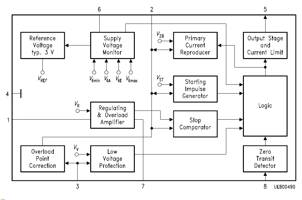
Page 80
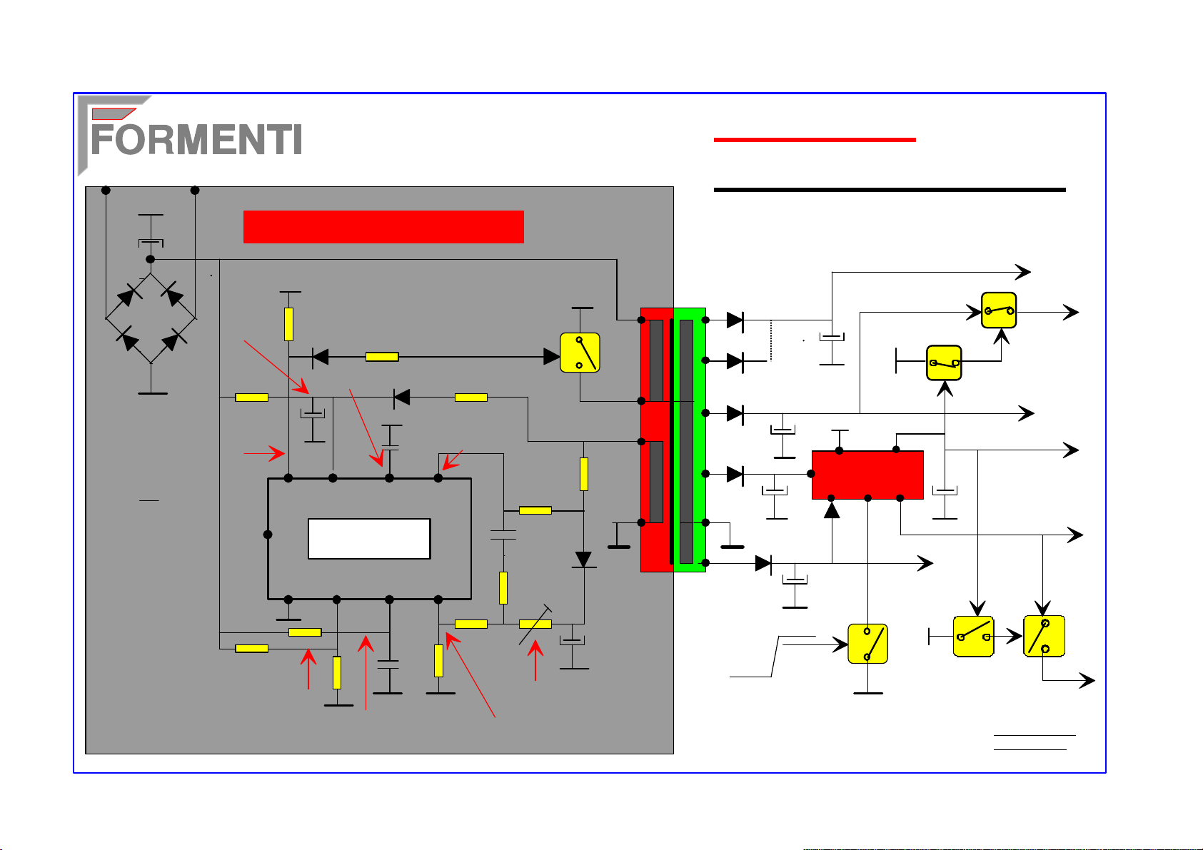
F 19
MAINS
INPUT
NON MAINS ISOLATED SECTOR
START-UP
R1
DRIVE
OUTPUT
PULSE
5
4 2
PRIMARY
VOLTAGE & CURRENT
SENSING
D13
SOFTSTART
6
D6
ZERO CROSSING
DETECTOR
7
SMPS CONTROL
IC1 TDA 4605
3
1
TR 1
STH7N80FI
8
OVER LOAD
PROTECTION
D8
R14
SUPPLY VOLTAGE
ADJUSTMENT
15
3
11
9
S.M.P.S.
(CONFIGURATION WITHOUT
ZERO POWER STAND BY MODULE)
148 V (110°)
2
4
128 V
10
8
6 / 16
12
T 1
FROM PIN 19
IC 100
SAA5297A
ON
OFF
5
2
1
TR 2
line output stage
489
TR3
TR 4
8,5v
26 V
sound
power
line driver
26 V
12 V
signal
processing
stand by
5 V
TR6
TR5
5 V
F19SMPS.DRW
E.G. 7/11/99
Page 81
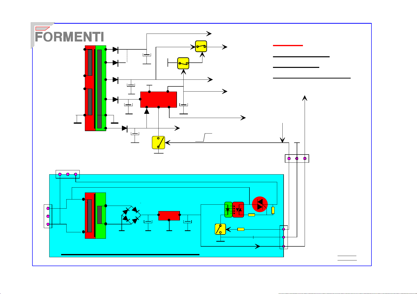
15
3
11
9
MAINS TO MAIN BOARD
T 1
148 V (110°)
2
4
128 V
10
8
6 / 16
12
5
2
TDA8183
1
TR 2
IC10
489
TR3
TR 4
8,5v
26 V
sound
power
line driver
signal
processing
OFF
ON
line output stage
26 V
12 V
5 V
F 19
LOW POWER
STAND-BY
CONFIGURATION
5 V
stand by
FROM PIN 19
IC 100
SAA5297A
T1
1
9
IC 1
FROM
MAINS
SWITCH
7
1
L7805CV
2
5
STAND-BY MODULE
TR2 BT808
IC2 IL410
3
X1
X2
X3
A12
ON-OFF
5 V ST-BY
F19LPSBC.DRW
E.G. 14 /11/99
Page 82

F19
F19
SERVICE MODE
SERVICE MODE
Page 83
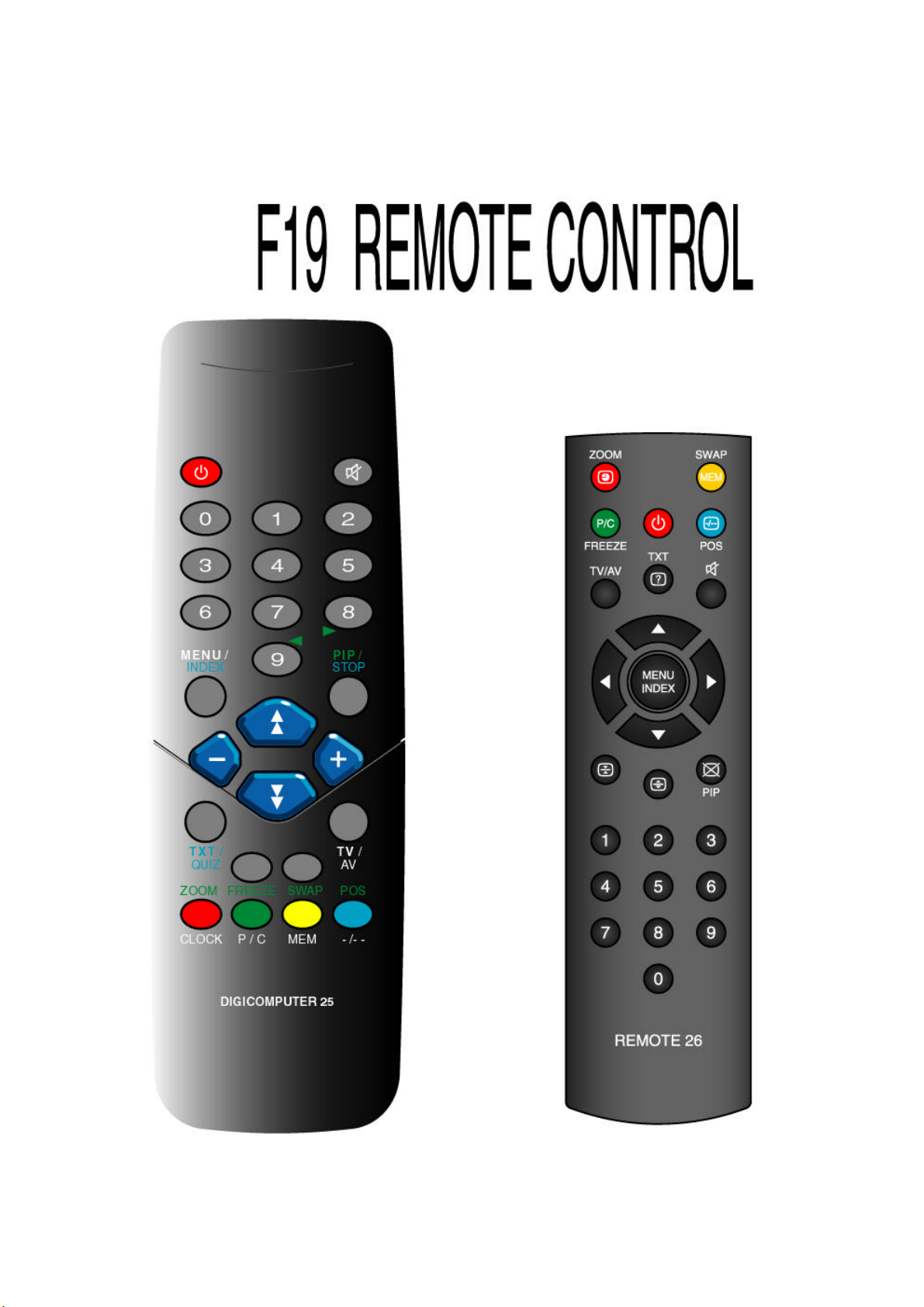
Page 84

For the description of the use of the TV make use of the Instruction Manual
Service mode
As already mentioned in the summary the remote control can be used to set all
parameter and to adjust the TV set without to open the back cover.
There are two ways to enter the "SERVICE MODE" that are to use the LOCAL
KEYBOARD or to have a precial prepared REMOTE CONTROL.
FIRST METHOD. (If the special remote control is available use the button following the
indication of the Table 1
Table 1 List of command of the "SERVICE REMOTE CONTROL"
BUTTON RC5 Sub
System
0 0 0 Vertical Slope
1 0 1 Vertical Amplitude
2 0 2 Vertical Shift
3 0 3 Vertical S Correctio
4 0 4 Horizontal Shift
5 0 5 HorizontalAmplitude
6 0 6 E-W parabola
7 0 7 E-W Corner
8 0 8 E-W Trapezium
9 0 9 AGC
Pr + 0 32 Up Carousel of all Service Parameter
Pr - 0 33 Down Carousel of all Service Parameter
Decimal Coce
Function
Vol + 0 16 Adjust Parameter Value (UP)
Vol - 0 17 Adjust Parameter Value (Down)
TV 0 63 Leave SERVICE MODE" without to store
MEM 0 50 Leave SERVICE MODE with store
MENU 0 53 Wred
SERVICE 7 58 SERVICE MODE ENTER
E.G.Data creazione 31/10/99 15.38 3 / 7 f19intro
Page 85
Table 2 Parameter and value to be adjusted in "SERVICE MODE"
PARAMETER VALUE DESCRIPTION
init ctvfor v0.6 on/ off Default Initialization
vg2test on/off Cut -off adjustment
txtbri 0--63 Adjust TXT brightness
txtcon 0--63 Adjust TXT Contrast
884c04 Bit (FSU)
884c03 Bit (FSU)
88c02 Bit (FSU)
optionb1 Bit (FSU) Select TV standard and TXT character set
optionb2 Bit (FSU) Scart type selections (
optionb3 Bit (FSU) (*) Hotel mode setting
nicamuperror 0--63 Nicam sensitivity (upper limit)
nicamlowerror 0--63 Nicam sensitivity (Lower limit).
nicamcon Bit (FSU) Tda9875 CONTROL
pipcontrast 0--15 PIP Contrast control
wblue 0--63 Blue channel gain
wgreen 0--63 “Green channel gain
wred 0--63 “Red channel gain
ydelaypal 0--63 Luma chroma delay
Increase blue stretch and the dynamic skin
Adj. acl (automatic colour limiter - and cathode drive level.
Adj.(black stretch), blue stretch, and the blue back
ewtrapeze 0--63 E-W- Trapezium adjustment
ewcorner 0--63 E-W- Corner Adjustment
ewparab 0--63 E-W- Parabola Adjustment
ewwidth 0--63 Horizontal Amplitude
h-shift 0--63 Horizontal shift
s-corr 0--63 Vertical S-Correction
v-shift 0--63 Shift Vertical
v-ampl 0--63 Vertical Amplitude
v-slope 0--63 Slope Vertical
agc 0--63 AGC adjustment
if xx afc 2/3 0--63 (FSU) Factory set up
LEGENDA: (FSU)= FACTORY SET UP (*) REDUCE OF A QUANITY 4 TO GET HOTEL MODE
WARNING!! Do not change value for those parameter that are highlighted please
E.G.Data creazione 31/10/99 15.38 5 / 7 f19intro
Page 86

Note 1
WARNING!!!!! The above procedure can be applied
only to TV set specially prepared for this functions
If during the installation of the TV set the AUTOSTORE" method is used, it is
fundamental, before to start the function, to select the name of the country as the criteria of
listing the broadcasters names is fixed by EBU table that are related to the country itself. It
is possible to find more channels of the same broadcaster on the Arial. In this case the
system will place first the signal having TXT with the strongest signal level than the others
and finally, with the found sequence the weakest one without TXT.
Note 2
To get HOTEL MODE it is necessary to enter "SERVICE MODE" and to change the
parameter "optionb3". Read the original value e subtract 4 (decimal). In HOTEL MODE all
tuning systems are not possible, the volume is pre fixed and the MENU from the LOCAL
KEY BOARD is not accessible.
Note 3
For fast programming (in case of installation of several TV set in Shops or Hotels a
"Black Box" is available on request. The procedure for a quick program is as follows:
1. Install and tune all channel storing it in the program sequence you want
2. Switch off the Set with the remote control and leave it in Stand-by mode
3. Switch on the "Black Box" and connect it to Scart
4. Press the button corresponding to the chassis to be programmed and at the same time
press the button "Read" for a while. (corresponding LED will be on.
5. When the LED "Write" became off (after few seconds) disconnect the "Black Box"
6. Insert the Black Box in the new TV set (in stand by condition)
7. Press F19 and "Write" buttons at same time. Corresponding "Write" LED will light
8. After few seconds when the "Write" LED will switch-off the procedure is finished .
9. Repeat points from 6 to 8 to program others TV set
E.G.Data creazione 31/10/99 15.38 6 / 7 f19intro
Page 87

Table 4 List of languages that can be reproduced as a function of the TXT characters set
Adding the value of the
setting with the optionb1 (bit number 6)
WEST EUROPE CHARACTER SET
LANGUAGES
ENGLISH POLISH
GERMAN GERMAN
SWEDISH ESTONIA
ITALIAN SERB-CROAT
FRENCH CZECH
SPANISH RUMEN
TURKISH
Just to give an example how to set the option byte 1, 2, and 3 we can start from
a TV set for BG standard, with hyperband tuner to be sold in a country using West
European character set.
Locking at the table 3 Optionb1 we have the following condition:
EAST EUROPE CHARACTER SET
LANGUAGES
BIT OPTIONB1
NUMBER 0 1 VALUE WEIGHT
0 BG 1 1
1 L/L' 0
2 I 0
3 DK 0
4 X 0
5 X 0
6 E.E.TXT W.E. TXT 1 64
7 CATV 1 128
became 0 that is the new value is 129 (128 plus 1)that in hexadecimal format is 41
last column we get 193
in decimal form and C!
in hexadecimal.
This means that we
have to choose this
value (C1) for the
optionb1 in service
mode
If we want to change from West Europe character set to East Europe, bit 6
REMEMBER TO INSERT COUNTRY TABLE
E.G.Data creazione 31/10/99 15.38 7 / 7 f19intro
Page 88

THE SECOND METHOD to enter service mode is to use the LOCAL KEY BOARD
as describe here below
1. Starting from TV off press VOLUME + on the LOCAL KEYBOARD and in the
mean time switch on the TV with the mains switch
2. Within three second switch on the TV using the "SWITCH-OFF" button on the
Remote Control
3. A small windows with black background and yellow characters will appear in the
middle of the screen.
4. Using the Remote control, program + / - (top bottom) will change the
"PARAMETER" and the VOLUME + / - (left / right) will change the value
5. Each parameter can be stored, leaving the service mode, by using the MEM
(yellow) button on the remote control
6. To leave "SERVICE MODE" without to store the new value use the TV button.
PARAMETER VALUE
7. It is not necessary to store each value one by one this means that you can
change all value you need and finally leave the SERVICE MODE pressing the
YELLOW button MEM.
In the Table 3 we can find all parameter and related value to be seated. Some
parameter have to adjusted with a simple on-off value, others are just factory option and
more others must be adjusted with value that are expressed in hexadecimal form ranging
from 0 to FF (that is from 0 to 63 in decimal form ).
Table 3 represent the value to be assigned to three parameter to properly set options:
Table 3 Option bye (1, 2 and 3) value and related meaning
BIT OPTIONB1 OPTIONB2 OPTIONB3
WEIGHT 0 1 0 1 0 1
0 BG 2° SCART FSU
1 L/L' MUST BE 1
2 I CINCH HOTEL
BACKGROUND
3 DK SVHS NTSC M
4 X RGB UV1316
5 X X V. GUARD
6 E.E.TXT W.E.TXT X
7 CATV X
E.G.Data creazione 31/10/99 15.38 4 / 7 f19intro
Page 89
PICTURE IN PICTURE
MODULE
Page 90

SDA 9288X
PICTURE IN PICTURE
1 General Description
The Picture-in-Picture Processor SDA 9288X A141 generates a picture of reduced size of
a video signal (inset channel) for the purpose of combining it with another video signal
(parent channel). The easy implementation of the IC in an existing system needs only a
few additional external components. There is a great variety of application facilities
professional and consumer products (TV sets, supervising monitors, multi-media, …)
Data Sheet
• 212 luminance and 53 chrominance pixels per inset line for picture size 1/9
• 6-bit amplitude resolution for each incoming signal component
• Field and frame mode display
• Horizontal and vertical filtering
• Special antialias filtering for the luminance signal
16:9 compatibility
• Operation in 4:3 and 16:9 sets
• 4:3 inset signals on 16:9 displays or v.v. with picture size 1/9 and 1/16, respectively
Analog inputs
• Y, + (B-Y), + (R-Y) or Y, -(B-Y), -(R-Y)
Analog outputs
• Y, + (B-Y), + (R-Y) or Y, – (B-Y), – (R-Y) or RGB
• 3 RGB matrices: EBU, NTSC (Japan), NTSC (USA)
Free programmable position of inset picture
• Steps of 1 pixel and 1 line
• All PIP and POP positions are possible
2 picture sizes
• 1/9 or 1/16 of normal size
High resolution display
13.5 MHz/27 MHz display clock frequency
Freeze picture
I 2 C Bus control
SDA 9288X P.I.P. Pagina 1 di 4 e.g. sda9288xR.doc
Page 91

Threefold PIP/POP facility
• Three different I 2 C-addresses (pin-programmable)
System Description
AD Conversion, Inset Synchronization
The inset video signal is fed to the SDA 9288X A141 as analog luminance and
chrominance components 1) . The polarity of the chrominance signals is programmable.
After clamping the video components are AD-converted with an amplitude resolution of 6
bit. The conversion is done using a 13.5 MHz clock for the luminance signal and a 3.375
MHz clock for the chrominance signals.
For the adaption to different application the clamp timing for the analog inputs can be
chosen (CLPS; CLPFIX). Setting this bits to ‘1’ can be useful for non-standard input
signals.
For inset synchronization it is possible to feed either a special 3-level signal via pin HVI
(detection of horizontal and vertical pulses) or separate signals via pins SCI for horizontal
and VI for vertical synchronization. SCI is the horizontal synchron signal of the inset
channel. If the burst gate pulse of the sandcastle is used it must be adapted to TTL
compatible levels by a simple external circuit. Centering of the displayed picture area is
possible by a programmable delay for the horizontal synchronization signal (HSIDEL).
The inset horizontal synchronization signals are sampled with 27 MHz. This 27 MHz clock
and the AD converter clocks are derived from the parent horizontal synchronization pulse
or from the quartz frequency converted by a factor of 4/3.
Delay differences between luminance and chrominance signals at the input of the IC
caused by chroma decoding are compensated by a programmable luminance delay line
(YDEL) of about – 290 ns … 740 ns (at decimation input
By analyzing the synchronization pulses the line standard of the inset signal source is
detected and interference noise on the vertical sync signal is removed. For applications
with fixed line standard (only 625 lines or 525 lines) the automatic detection can be
switched off.
The phase of the vertical sync pulse is programmable (VSIDEL; VSPDEL). By this way a
correct detection of the field number is possible, an important condition for frame mode
display.
Input Signal Processing
SDA 9288X P.I.P. Pagina 2 di 4 e.g. sda9288xR.doc
Page 92

This stage performs the decimation of the inset signal by horizontal and vertical filtering
and sub-sampling. A special antialias filter improves the frequency response of the
luminance channel. It is optimized for the use of the horizontal decimation factor 3:1.
A window signal, derived from the sync pulses and the detected line standard, defines the
part of the active video area used for decimation. For HSIDEL = ‘0’ the decimation window
is opened about 104 clock periods (13.5 MHz) after the horizontal synchronization pulse.
For the 625 lines standard the 36th video line is the first decimated line, for the 525 lines
standard decimation starts in the 26th video line.
The realized chrominance filtering allows omitting the color decoder delay line for PAL and
SECAM demodulation if the color decoder supplies the same output voltages independent
of the kind of operation. In case of SECAM signals an amplification of the chrominance
signals by a factor of 2 is necessary because just every second line a signal is present.
This chrominance amplification is programmable via pin SYS or I 2 C Bus (AMSEC). The
horizontal and vertical decimation factors are free programmable (DECHOR, DECVER).
Using different decimations horizontal and vertical 16:9 applications become realizable:
DECHOR = ‘1’, DECVER = ‘0’: picture size 1/9 for 4:3 inset signals on 16:9 displays
DECHOR = ‘0’, DECVER = ‘1’: picture size 1/16 for 16:9 inset signals on 4:3 displays
PIP Field Memory
The on-chip memory stores one decimated field of the inset picture. Its capacity is 169 812
bits. The picture size depends on the horizontal and vertical decimation factors.
In field mode display just every second inset field is written into the memory, in frame
mode display the memory is continuously written. Data are written with the lower inset
clock frequency depending on the horizontal decimation factor (4.5 MHz or 3.375 MHz).
Normally the read frequency is 13.5 MHz and 27 MHz for scan conversion systems.
For progressive scan conversion systems and HDTV displays a line doubling mode is
available (LINEDBL). Every line of the inset picture is read twice. Memory writing can be
stopped by program (FREEZE), a freeze picture display results (one field).
Having no scan conversion and the same line numbers in inset and parent channel (625
lines or 525 lines both) frame mode display is possible. The result is a higher vertical and
time resolution because of displaying every incoming field. For this purpose the standards
are internally analysed and activating of frame mode display is blocked automatically when
the described restrictions are not fulfilled.
As in the inset channel a field number detection is carried out for the parent channel.
SDA 9288X P.I.P. Pagina 3 di 4 e.g. sda9288xR.doc
Page 93

Depending on the phase between inset and parent signals a correction of the display
raster for the read out data is performed by omitting or inserting lines when the read
address counter outruns the write address counter.
The display position of the inset picture is free programmable (POSHOR, POSVER).
The first possible picture position (without frame) is 54 clock periods (13.5 MHz or 27 MHz)
after the horizontal and 4 lines after the vertical synchronization pulses. Starting at this
position the picture can be moved over the whole display area. Even POP-positions
(Picture Outside Picture) at 16:9 applications are possible.
Horizontal Decimation PIP PIXELS per Line
Having different line standards in inset and parent channels we have a so called mixed
mode display. It causes deformations in the aspect ratio of the inset picture. A special
mixed mode display is available for the picture size 1/9 (MIXDIS):
Synchronization of memory reading with the parent channel is achieved by processing
the parent horizontal and vertical synchronization signals in the same way as described
for the inset channel. The synchronization signals are fed to the IC at pin HP/SCP for
horizontal synchronization and pin VP for vertical synchronization. In the same way as
described for the inset channel the burst gate of the sandcastle signal can be used for
horizontal synchronization. In scan conversion systems also the inputs HPD/SCI and
VPD/VI are available if the input HVI is activated for inset synchronization.
2.4 Output Signal Processing
At the memory output the chrominance components are demultiplexed and linearly
interpolated to the luminance sample rate. Different output formats are available:
luminance signal Y with inverted or non-inverted chrominance signals (B-Y), (R-Y) or RGB.
For the RGB conversion 3 matrices are integrated: Matrix selection is done by pin SYS or I
2 C Bus. The matrices are designed for the following input voltages (100 % white, 75 %
color saturation):
SDA 9288X P.I.P. Pagina 4 di 4 e.g. sda9288xR.doc
Page 94
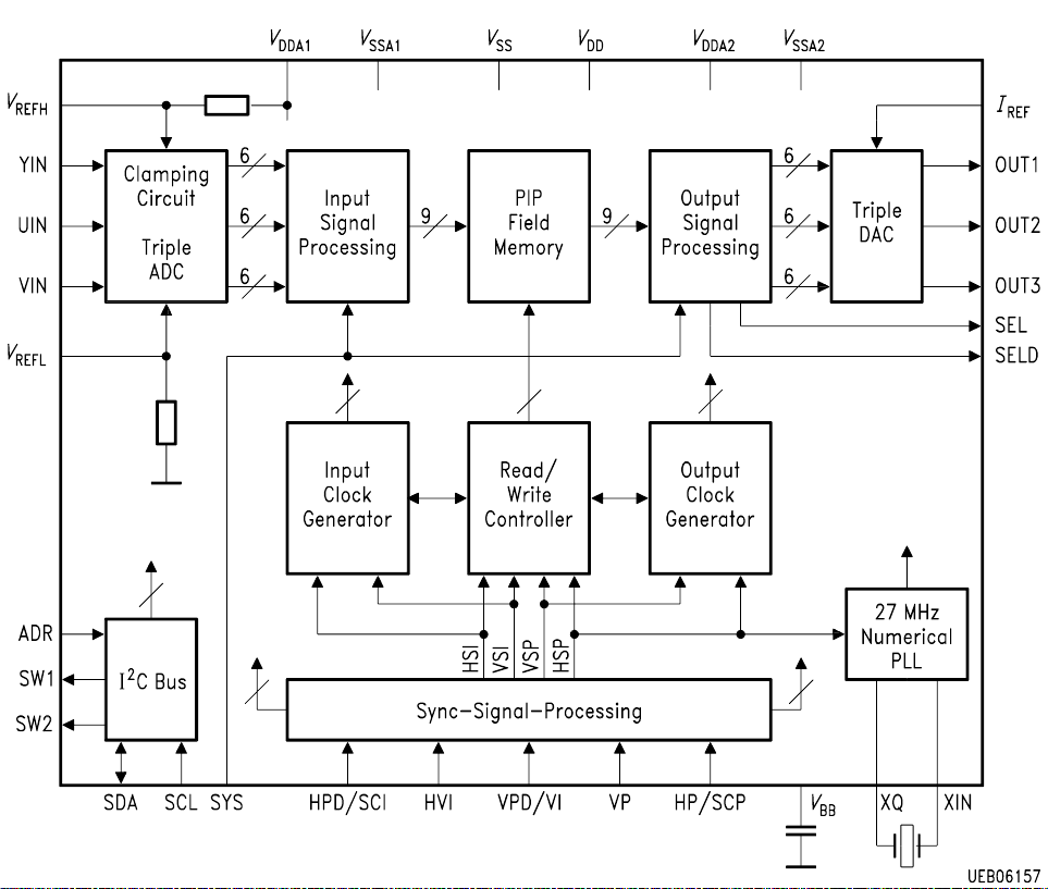
Page 95
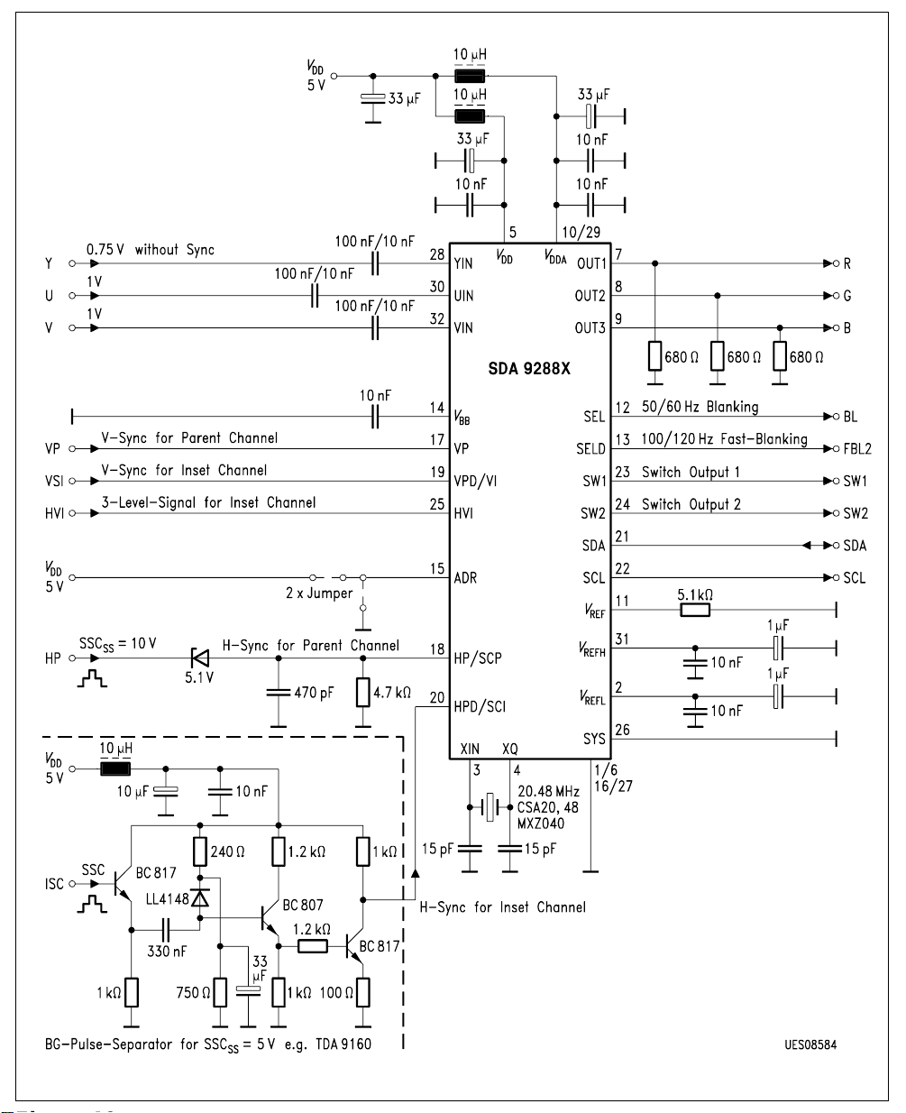
Page 96

TDA8310A
PAL/NTSC colour processor
for PIP applications
FEATURES
• Video switch with 2 CVBS inputs. One input can beswitched between CVBS and Y/C and the circuit can
automatically detect whether the incoming signal is CVBS or Y/C
• Integrated chrominance trap and bandpass filters (automatically calibrated)
• Integrated luminance delay line
• Automatic PAL/NTSC decoder which can decode all standards available in the world
• Easy interfacing with the TDA8395 (SECAM decoder) for multistandard applications
• Horizontal PLL with an alignment-free horizontal oscillator
• Vertical count-down circuit
• RGB/YUV and fast blanking switch with 3-state output and active clamping
• Low dissipation (560 mW)
• Small amount of peripheral components compared with competition Ics
GENERAL DESCRIPTION
The TDA8310A is an alignment-free PAL/NTSC colour processor for Picture-in-Picture (PIP) applications.
The main difference between the TDA8310 and the TDA8310A is that the vision IF amplifier has been omitted
in the TDA8310A. Therefore, the circuit contains an input signal selector, a PAL/NTSC colour decoder, horizontal
and vertical synchronization and an RGB/YUV switch.
The input signal selector has 2 CVBS inputs. One of the inputs can be switched between CVBS and Y/C and the
circuit can automatically detect whether the incoming signal is CVBS or Y/C. The output signals for the PIP
processor are:
• Luminance signal
• Colour difference signals (U and V)
• Horizontal and vertical synchronization pulses.
• The RGB/YUV switch can select between two RGB or YUV sources, e.g. between the PIP processor and the
SCART input signal.
• The supply voltage for the IC is 8 V. It is available in a 52-pin SDIP package.
FUNCTIONAL DESCRIPTION
CVBS switch
The circuit contains a 2 input CVBS switch and one of the inputs can be switched between CVBS and Y/C.
The circuit contains an identification circuit which can automatically switch between the CVBS and Y/C signals.
It is also possible to force the switch to CVBS or Y/C.
TDA8310A CHROMA DECODER FOR PIP Pagina 1 di 2 e.g. TDA8310A.doc
Page 97

Synchronization circuit
The sync separator is preceded by a voltage controlled amplifier which adjusts the sync pulse amplitude to a fixed
level. The sync pulses are fed to the slicing stage (separator) which operates at 50% of the amplitude.
The separated sync pulses are fed to the first phase detector and to the coincidence detector. The coincidence
detector is used to detect whether the line oscillator is synchronized and for transmitter identification. The first
PLL has a very high static steepness this ensures that the phase of the picture is independent of the line
frequency.
The line oscillator operates at twice the line frequency. The oscillator network is internal. Because of the spread of
internal components an automatic adjustment circuit has been added to the IC.
The circuit compares the oscillator frequency with that of the crystal oscillator in the colour decoder. This results in
a free-running frequency which deviates less than 2% from the typical value.
The horizontal output pulse is derived from the horizontal oscillator via a pulse shaper. The pulse width of the
output pulse is 5.4 ms, the front edge of this pulse coincides with the front edge of the sync pulse at the input.
The vertical output pulse is generated by a count-down circuit. The pulse width is approximately 380 ms. Both the
horizontal and vertical output pulses will always be available at the outputs even when no input signal is
available. In addition to the horizontal and vertical sync pulse outputs
the IC has a sandcastle pulse output which contains burst key and blanking pulses.
Integrated video filters
The circuit contains a chrominance bandpass and trap circuit. The filters are realised by gyrator circuits that are
automatically tuned by comparing the tuning frequency with the crystal frequency of the decoder. When a Y/C
signal is supplied to the input the chrominance trap is automatically switched off by the Y/C detection circuit
however, it is also possible to force the filters in the CVBS or Y/C position.
The luminance delay line is also realised by gyrator circuits.
Colour decoder
The colour decoder contains an alignment-free crystal oscillator, a colour killer circuit and colour difference
demodulators. The 90° phase shift for the reference signal is achieved internally.
The colour decoder is very flexible. Together with the SECAM decoder (TDA8395) an automatic multistandard
decoder can be designed but it is also possible to use it for one standard when only one crystal is connected to the
IC.
The decoder can be forced to one of the standards via the ‘forced mode’ pins. The crystal pins which are not used
must be connected to the positive supply line via a 8.2 κΩ resistor. It is also possible to connect the non-used pins
with one resistor to the positive supply line. In this event the resistor must have a value of 8.2 κΩ divided by the
number of pins.
The chrominance output signal of the video switch is externally available and must be used as an input signal
for the SECAM decoder.
RGB/YUV switch
The RGB/YUV switch is for switching between two RGB or YUV video sources. The outputs of the switch can be
set to high-impedance state so that other switches can be used in parallel.
The switch is controlled via pins 13 and 52.
TDA8310A CHROMA DECODER FOR PIP Pagina 2 di 2 e.g. TDA8310A.doc
Page 98
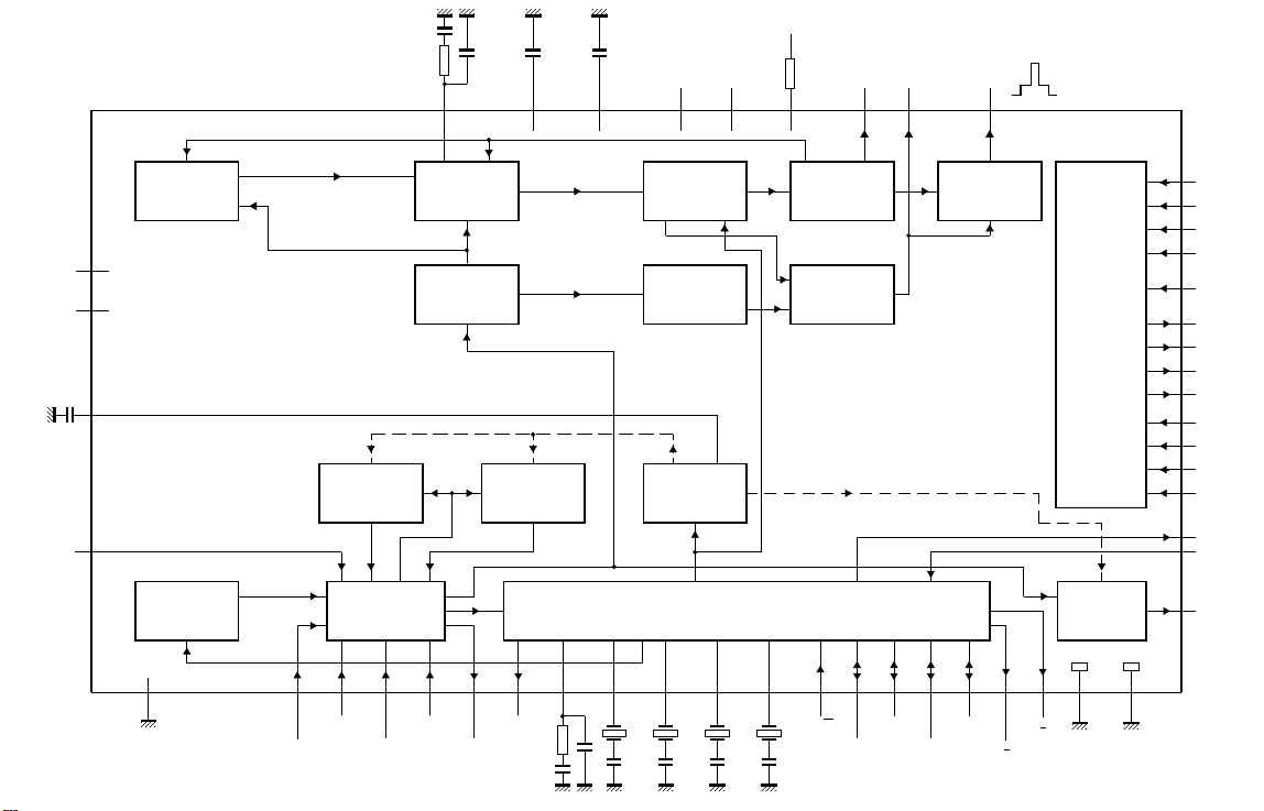
PH1LF
37
DEC
35
BG
DEC
21
DIG
INTB
V
V
P1
P2
41
19
30
HOUT36VOUT
39
SAND
40
CVBS
DEC
SW
n.c.
COINCIDENCE/
NOISE
DETECTOR
22, 29
i.c.
33, 34
FT
15
CHROMINANCE
BANDPASS
32
AUTOMATIC
DETECTOR
31
GND2
Y/C
CVBS
20
CVBS
INT
INPUT
SELECTOR
EXT
SYST
917
CHROMA
SW
PHASE
DETECTOR
SYNC
SEPARATOR
CHROMINANCE
4716
I
CHROMA
TRAP
48
SECAM
O
46 45
PLL XTAL4
VCO
+
CONTROL
VERTICAL
SYNC
SEPARATOR
FILTER
TUNING
REF
PAL/NTSC
DECODER
44
XTAL343XTAL242XTAL1
PULSE
SHAPER
HORIZONTAL/
VERTICAL
DIVIDER
TDA8310A
27 26
R/W
COLOUR2
COLOUR1
25
LOGIC1
SANDCASTLE
GENERATOR
24
23
LOGIC2
B Y
50 51
R Y
RGB/YUV
SWITCH
LUMINANCE
DELAY LINE
18 38
GND1 GND3
10
R1
11
G1
12
B1
13
BLANK1
14
CLAMP
8
R
7
G
6
B
5
BLANK
1
R2
2
G2
3
B2
52
BLANK2
4
IDENT
HUE
28
49
Y
MGD128
Page 99

PINNING
SYMBOL PIN DESCRIPTION
R2 1 RED input 2 (PIP)
G2 2 GREEN input 2 (PIP)
B2 3 BLUE input 2 (PIP)
IDENT 4 colour standard identification output
BLANK 5 blanking output
B 6 BLUE output
G 7 GREEN output
R 8 RED output
SYST
SW
9 CVBS/system switch
R1 10 RED input 1
G1 11 GREEN input 1
B1 12 BLUE input 1
BLANK1 13 blanking input 1
CLAMP 14 clamping pulse input
DEC
FT
CHROMA
CVBS
EXT
15 decoupling filter tuning
16 chrominance input
I
17 external CVBS/Y input
GND1 18 ground 1 (0 V)
V
P1
CVBS
DEC
INT
DIG
19 supply voltage 1 (+8 V)
20 internal CVBS input
21 decoupling digital supply rail
i.c. 22 internally connected (test purposes)
LOGIC2 23 crystal logic 2 input/output
LOGIC1 24 crystal logic 1 input/output
COLOUR2 25 colour system logic 2 input/output
COLOUR1 26 colour system logic 1 input/output
W 27 read/write selection input
R/
SYMBOL PIN DESCRIPTION
HUE 28 HUE control input
i.c. 29 internally connected (test purposes)
INTB 30 internal bias
GND2 31 ground 2 (0 V)
CVBS
SW
32 CVBS positive/negative modulation
control switch input
n.c. 33 not connected
n.c. 34 not connected
DEC
BG
35 bandgap decoupling
VOUT 36 vertical sync output pulse
PH1LF 37 phase 1 loop filter
GND3 38 ground 3 (0 V)
HOUT 39 horizontal sync output pulse
SAND 40 sandcastle pulse output
V
P2
41 supply voltage 2 (+8 V)
XTAL1 42 4.4336 MHz crystal
XTAL2 43 3.5820 MHz crystal for PAL-N
XTAL3 44 3.5756 MHz crystal for PAL-M
XTAL4 45 3.5795 MHz crystal for NTSC
PLL 46 PLL colour filter
CHROMA
47 chrominance output for TDA8395
O
SECAM 48 SECAM reference output
Y 49 Y output
B−Y50B−Y output
R−Y51R−Y output
BLANK2 52 blanking/insertion input 2 (PIP)
Page 100

TDA8395
SECAM DECODER
FEATURES
• Fully integrated filters
• Alignment free
• For use with baseband delay
GENERAL DESCRIPTION
The TDA8395 is a self-calibrating, fully integrated SECAM decoder. The IC should
preferably be used in conjunction with the PAL/NTSC decoder TDA8362 or TDA8366 and
with the switched capacitor baseband delay circuit TDA4660. The IC incorporates HF and
LF filters, a demodulator and an identification circuit (luminance is not processed in this
IC). The IC needs no adjustments and very few external components are required. A
highly stable reference frequency is required for calibration and a two-level sandcastle
pulse for blanking and burst gating.
FUNCTIONAL DESCRIPTION
The TDA8395 is a self-calibrating SECAM decoder designed for use with a baseband
delay circuit.
During frame retrace a 4.433619 MHz reference frequencyis used to calibrate the filters
and the demodulator. Thereference frequency should be very stable during this period.
The Cloche filter is a gyrator-capacitor type filter theresonance frequency of which is
controlled during the calibration period and offset during scan; this ensures thecorrect
frequency during calibration.
The demodulator is a Phase-Locked Loop (PLL) type demodulator which uses the
frequency reference and the bandgap reference to force the PLL to the required
demodulation characteristic.
The low frequency de-emphasis is matched to the PLL and is controlled by the tuning
voltage of the PLL.
Secam secoder TDA8395 Pagina 1 di 2 e.g.TDA8395R
 Loading...