

Force SPARC/CPCI-520G, SPARC/CPCI-522G, SPARC/CPCI-522, SPARC/CPCI-523G Technical Reference Manual
Page 1

SPARC/CPCI-52x(G)
Technical Reference Manual
P/N 208914 Edition 2.0
November 2000
Force Computers GmbH
All Rights Reserved
This document shall not be duplicated, nor its conten ts used
for any purpose, unless written per mi ssio n has be e n granted.
Copyright by Force Computers
Page 2

World Wide Web: www.forcecomputers.com
24-hour access to on-line manuals, driver updates, and application notes
is provided v i a SMART, our SolutionsPLUS customer support program
that provides current technical and services information.
Headquarters
The Americas Europe Asia
Force Computers Inc.
5799 Fontanoso Way
San Jose, CA 95138-1015
U.S.A.
Tel.: +1 (408) 369-6000
Fax: +1 (408) 371-3382
Email [email protected]
The information in this document has been carefully checked and is believed to be entirely reliable. Force Computers makes no warranty of any kind with regard
to the material in this document, and assumes no responsibility for any errors which may appear in this document. Force Computers reserves the right to make
changes without notice to this, or any of its products, to improve reliability, performance, or design.
Force Computers assumes no responsibility for the use of any circuitry other than circuitry which is part of a product of Force Computers GmbH. Force
Computers does not convey to the purchaser of the product described herein any license under the patent rights of Force Computers GmbH nor the rights of
others. All product names as mentioned herein are the trademarks or registered trademarks of their respective companies.
Force Computers GmbH
Prof.-Messerschmitt-Str. 1
D-85579 Neubiberg/München
Germany
Tel.: +49 (89) 608 14-0
Fax: +49 (89) 609 77 93
Email [email protected]
NOTE
Force Computers Japan KK
Shiba Daimon MF Building 4F
2-1-16 Shiba Daimon
Minato-ku, Tokyo 105-0012
Japan
Tel.: +81 (03) 3437 3948
Fax: +81 (03) 3437 3968
Email [email protected]
Page 3

Contents
Table of Contents
Using This Manual . . . . . . . . . . . . . . . . . . . . . . . . . . . . . . . . . . . . . . . . . . . . . . . . . . . . . . . . . .vii
1 Safety Notes . . . . . . . . . . . . . . . . . . . . . . . . . . . . . . . . . . . . . . . . . . . . . . . . . . . . . . . . . . . . . . . . . 1
2 Introduction . . . . . . . . . . . . . . . . . . . . . . . . . . . . . . . . . . . . . . . . . . . . . . . . . . . . . . . . . . . . . . . . . 5
2.1 Product Nomenclature . . . . . . . . . . . . . . . . . . . . . . . . . . . . . . . . . . . . . . . . . . . . . . . . . . . 8
2.2 Ordering Information . . . . . . . . . . . . . . . . . . . . . . . . . . . . . . . . . . . . . . . . . . . . . . . . . . . . 9
3 Installation . . . . . . . . . . . . . . . . . . . . . . . . . . . . . . . . . . . . . . . . . . . . . . . . . . . . . . . . . . . . . . . . . 11
3.1 Installation Prerequisites and Requirements . . . . . . . . . . . . . . . . . . . . . . . . . . . . . . . . 14
3.1.1 Requirements . . . . . . . . . . . . . . . . . . . . . . . . . . . . . . . . . . . . . . . . . . . . . . . . . . . 14
3.1.2 Memory Modules . . . . . . . . . . . . . . . . . . . . . . . . . . . . . . . . . . . . . . . . . . . . . . . 17
3.1.3 Solaris Installation . . . . . . . . . . . . . . . . . . . . . . . . . . . . . . . . . . . . . . . . . . . . . . . 18
3.1.4 Terminal connection . . . . . . . . . . . . . . . . . . . . . . . . . . . . . . . . . . . . . . . . . . . . . 20
4 Base-520(G) Installation . . . . . . . . . . . . . . . . . . . . . . . . . . . . . . . . . . . . . . . . . . . . . . . . . . . . . . 21
4.1 Location Overview . . . . . . . . . . . . . . . . . . . . . . . . . . . . . . . . . . . . . . . . . . . . . . . . . . . . . 21
4.2 Mechanical Construction . . . . . . . . . . . . . . . . . . . . . . . . . . . . . . . . . . . . . . . . . . . . . . . . 23
4.2.1 FORCE COMPUTERS UPA64S Card Installation . . . . . . . . . . . . . . . . . . . . . 25
4.3 Powering Up . . . . . . . . . . . . . . . . . . . . . . . . . . . . . . . . . . . . . . . . . . . . . . . . . . . . . . . . . . 26
4.4 Switch Settings . . . . . . . . . . . . . . . . . . . . . . . . . . . . . . . . . . . . . . . . . . . . . . . . . . . . . . . . 27
4.5 Front Panel and Connectors . . . . . . . . . . . . . . . . . . . . . . . . . . . . . . . . . . . . . . . . . . . . . 28
4.5.1 Audio Interface . . . . . . . . . . . . . . . . . . . . . . . . . . . . . . . . . . . . . . . . . . . . . . . . . 31
4.5.2 Ethernet Interfaces . . . . . . . . . . . . . . . . . . . . . . . . . . . . . . . . . . . . . . . . . . . . . . . 32
4.5.3 SCSI #1 Connector Pinout . . . . . . . . . . . . . . . . . . . . . . . . . . . . . . . . . . . . . . . . 33
4.5.4 Serial I/O Interface Connector Pinout . . . . . . . . . . . . . . . . . . . . . . . . . . . . . . . . 34
4.5.5 Keyboard/Mouse Connector . . . . . . . . . . . . . . . . . . . . . . . . . . . . . . . . . . . . . . . 35
4.5.6 CompactPCI Backplane Connector Pinout . . . . . . . . . . . . . . . . . . . . . . . . . . . . 36
SPARC/CPCI-52x(G) Page i
Page 4

Contents
4.6 SCSI #1 Configuration . . . . . . . . . . . . . . . . . . . . . . . . . . . . . . . . . . . . . . . . . . . . . . . . . . 38
4.7 Ethernet Address and Host ID . . . . . . . . . . . . . . . . . . . . . . . . . . . . . . . . . . . . . . . . . . . 41
4.8 OpenBoot Firmware . . . . . . . . . . . . . . . . . . . . . . . . . . . . . . . . . . . . . . . . . . . . . . . . . . . . 42
4.8.1 Boot the System . . . . . . . . . . . . . . . . . . . . . . . . . . . . . . . . . . . . . . . . . . . . . . . . . 42
4.8.2 NVRAM Boot Parameters . . . . . . . . . . . . . . . . . . . . . . . . . . . . . . . . . . . . . . . . . 46
4.8.3 Diagnostics . . . . . . . . . . . . . . . . . . . . . . . . . . . . . . . . . . . . . . . . . . . . . . . . . . . . 46
4.8.4 Display System Information . . . . . . . . . . . . . . . . . . . . . . . . . . . . . . . . . . . . . . . 49
4.8.5 Reset the System . . . . . . . . . . . . . . . . . . . . . . . . . . . . . . . . . . . . . . . . . . . . . . . . 50
4.8.6 OpenBoot Help . . . . . . . . . . . . . . . . . . . . . . . . . . . . . . . . . . . . . . . . . . . . . . . . . 50
5 I/O-52x(G) Installation . . . . . . . . . . . . . . . . . . . . . . . . . . . . . . . . . . . . . . . . . . . . . . . . . . . . . . . 53
5.1 Location Overview . . . . . . . . . . . . . . . . . . . . . . . . . . . . . . . . . . . . . . . . . . . . . . . . . . . . . 53
5.2 Mechanical Constructions . . . . . . . . . . . . . . . . . . . . . . . . . . . . . . . . . . . . . . . . . . . . . . . 55
5.2.1 Installation/Deinstallation of the I/O-52x(G) . . . . . . . . . . . . . . . . . . . . . . . . . . 56
5.3 Powering Up . . . . . . . . . . . . . . . . . . . . . . . . . . . . . . . . . . . . . . . . . . . . . . . . . . . . . . . . . . 57
5.4 Front Panel and Connectors . . . . . . . . . . . . . . . . . . . . . . . . . . . . . . . . . . . . . . . . . . . . . 57
5.4.1 Ethernet #2 Interfaces . . . . . . . . . . . . . . . . . . . . . . . . . . . . . . . . . . . . . . . . . . . . 58
5.4.2 PMC Slots . . . . . . . . . . . . . . . . . . . . . . . . . . . . . . . . . . . . . . . . . . . . . . . . . . . . . 59
5.4.3 CompactPCI Backplane Connector Pinout . . . . . . . . . . . . . . . . . . . . . . . . . . . . 59
5.5 SCSI #2 Configuration . . . . . . . . . . . . . . . . . . . . . . . . . . . . . . . . . . . . . . . . . . . . . . . . . . 62
5.6 Ethernet #2 Configuration . . . . . . . . . . . . . . . . . . . . . . . . . . . . . . . . . . . . . . . . . . . . . . . 62
5.7 OpenBoot Firmware Alias Definitions for I/O-52x(G) . . . . . . . . . . . . . . . . . . . . . . . . 63
6 Hardware Description . . . . . . . . . . . . . . . . . . . . . . . . . . . . . . . . . . . . . . . . . . . . . . . . . . . . . . . 65
6.1 Processor – UltraSPARC-IIi . . . . . . . . . . . . . . . . . . . . . . . . . . . . . . . . . . . . . . . . . . . . . 68
6.1.1 Physical Memory Map . . . . . . . . . . . . . . . . . . . . . . . . . . . . . . . . . . . . . . . . . . . 69
6.1.2 External Cache Control Unit . . . . . . . . . . . . . . . . . . . . . . . . . . . . . . . . . . . . . . . 70
6.1.3 Memory Controller Unit, Memory Modules, and Main Memory Configuration .
70
6.1.4 Interrupt Map . . . . . . . . . . . . . . . . . . . . . . . . . . . . . . . . . . . . . . . . . . . . . . . . . . . 72
6.1.5 UltraSPARC-IIi PCI Bus Interface . . . . . . . . . . . . . . . . . . . . . . . . . . . . . . . . . . 74
6.2 APB (Advanced PCI Bridge) and CompactPCI Interface . . . . . . . . . . . . . . . . . . . . . 75
6.3 Ethernet and EBus2 Devices – PCIO . . . . . . . . . . . . . . . . . . . . . . . . . . . . . . . . . . . . . . 75
Page ii SPARC/CPCI-52x(G)
Page 5

Contents
6.3.1 Ethernet Interface – PCIO . . . . . . . . . . . . . . . . . . . . . . . . . . . . . . . . . . . . . . . . . 76
6.3.2 EBus2 Interface – PCIO . . . . . . . . . . . . . . . . . . . . . . . . . . . . . . . . . . . . . . . . . . 77
6.3.3 Boot PROM, Boot and User Flash EPROM . . . . . . . . . . . . . . . . . . . . . . . . . . . 79
6.3.4 Serial Interfaces – SAB 82532 . . . . . . . . . . . . . . . . . . . . . . . . . . . . . . . . . . . . . 80
6.3.5 Keyboard/Mouse, FDC and Parallel Interface – Super I/O . . . . . . . . . . . . . . . . 81
6.3.6 RTC/NVRAM – M48T58 . . . . . . . . . . . . . . . . . . . . . . . . . . . . . . . . . . . . . . . . . 83
6.3.7 Audio Interface – CS4231A . . . . . . . . . . . . . . . . . . . . . . . . . . . . . . . . . . . . . . . 84
6.3.8 System Configuration Registers – SCR . . . . . . . . . . . . . . . . . . . . . . . . . . . . . . 85
6.3.9 SCR: Front Panel and Switches . . . . . . . . . . . . . . . . . . . . . . . . . . . . . . . . . . . . . 86
6.3.10 SCR: Boot and User Flash . . . . . . . . . . . . . . . . . . . . . . . . . . . . . . . . . . . . . . . . . 89
6.3.11 SCR: Watchdog, Temperature Sensors, and Reset . . . . . . . . . . . . . . . . . . . . . . 90
6.3.12 SCR: ENUM Interrupt . . . . . . . . . . . . . . . . . . . . . . . . . . . . . . . . . . . . . . . . . . . . 94
2
6.3.13 SCR: I
C-Bus . . . . . . . . . . . . . . . . . . . . . . . . . . . . . . . . . . . . . . . . . . . . . . . . . . 95
6.4 SCSI Interface – SYM53C875 . . . . . . . . . . . . . . . . . . . . . . . . . . . . . . . . . . . . . . . . . . . . 97
6.5 PMC Slots with Busmode Support . . . . . . . . . . . . . . . . . . . . . . . . . . . . . . . . . . . . . . . . 98
7 FORCE OpenBoot Enhancements . . . . . . . . . . . . . . . . . . . . . . . . . . . . . . . . . . . . . . . . . . . . 101
7.1 System Configuration . . . . . . . . . . . . . . . . . . . . . . . . . . . . . . . . . . . . . . . . . . . . . . . . . . 102
7.1.1 System Configuration Register Accesses . . . . . . . . . . . . . . . . . . . . . . . . . . . . 102
7.1.2 LEDs, Seven Segment Display and Rotary Switch . . . . . . . . . . . . . . . . . . . . . 106
7.1.3 ID PROM . . . . . . . . . . . . . . . . . . . . . . . . . . . . . . . . . . . . . . . . . . . . . . . . . . . . 107
7.1.4 Viewing the Switch Status and Controlling the Temperature Sensors . . . . . . 108
7.1.5 PCI-Probing – NVRAM Configuration Variables . . . . . . . . . . . . . . . . . . . . . 109
7.2 Flash EPROM Support . . . . . . . . . . . . . . . . . . . . . . . . . . . . . . . . . . . . . . . . . . . . . . . . 110
7.2.1 Flash EPROM Programming . . . . . . . . . . . . . . . . . . . . . . . . . . . . . . . . . . . . . . 110
7.2.2 Flash EPROM Device Node . . . . . . . . . . . . . . . . . . . . . . . . . . . . . . . . . . . . . . 112
7.2.3 Loading and Executing Programs from User Flash EPROM . . . . . . . . . . . . . 115
7.3 Hardware Dependencies . . . . . . . . . . . . . . . . . . . . . . . . . . . . . . . . . . . . . . . . . . . . . . . . 116
7.3.1 Copying the OpenBoot Image from Boot PROM to Boot Flash EPROM . . . 116
7.3.2 Drop-in Drivers . . . . . . . . . . . . . . . . . . . . . . . . . . . . . . . . . . . . . . . . . . . . . . . . 118
7.3.3 Flash Memory Driver . . . . . . . . . . . . . . . . . . . . . . . . . . . . . . . . . . . . . . . . . . . 118
Product Error Report
SPARC/CPCI-52x(G) Page iii
Page 6

Contents
Page iv SPARC/CPCI-52x(G)
Page 7

Tables and Figures
List of Tables and Figures
Page Tab./Fig.
History of manual publication . . . . . . . . . . . . . . . . . . . . . . . . . . . . . . . . . . . . . . . . .ix Tab. a
Fonts, notations and conventions . . . . . . . . . . . . . . . . . . . . . . . . . . . . . . . . . . . . . . x Tab. b
Product naming conventions . . . . . . . . . . . . . . . . . . . . . . . . . . . . . . . . . . . . . . . . . . x Tab. c
Specifications of the SPARC/CPCI-52x(G) . . . . . . . . . . . . . . . . . . . . . . . . . . . . . . 7 Tab. 1
Nomenclature of the SPARC/CPCI-52x(G) . . . . . . . . . . . . . . . . . . . . . . . . . . . . . . 8 Tab. 2
Excerpt from the product’s ordering information . . . . . . . . . . . . . . . . . . . . . . . . . . 9 Tab. 3
SPARC/CPCI-520G (schematic view) . . . . . . . . . . . . . . . . . . . . . . . . . . . . . . . . . 11 Fig. 1
SPARC/CPCI-522 (schematic view) . . . . . . . . . . . . . . . . . . . . . . . . . . . . . . . . . . . 11 Fig. 2
SPARC/CPCI-522G (schematic view) . . . . . . . . . . . . . . . . . . . . . . . . . . . . . . . . . 12 Fig. 3
SPARC/CPCI-523G (schematic view) . . . . . . . . . . . . . . . . . . . . . . . . . . . . . . . . . 12 Fig. 4
Schematic exploded mechanical construction view . . . . . . . . . . . . . . . . . . . . . . . 13 Fig. 5
Maximum power supply values without UPA64S card and PMC modules . . . . . 15 Tab. 4
Environmental requirements of the SPARC/CPCI-52x(G) . . . . . . . . . . . . . . . . . . 15 Tab. 5
Audio interfaces requirements . . . . . . . . . . . . . . . . . . . . . . . . . . . . . . . . . . . . . . . . 16 Tab. 6
Qualified memory modules . . . . . . . . . . . . . . . . . . . . . . . . . . . . . . . . . . . . . . . . . . 17 Tab. 7
MEM-50 – memory module numbering scheme . . . . . . . . . . . . . . . . . . . . . . . . . . 17 Fig. 6
Qualified memory configurations (all data in MByte) . . . . . . . . . . . . . . . . . . . . . 18 Tab. 8
Required Solaris Packages . . . . . . . . . . . . . . . . . . . . . . . . . . . . . . . . . . . . . . . . . . 19 Tab. 9
Customizing Solaris . . . . . . . . . . . . . . . . . . . . . . . . . . . . . . . . . . . . . . . . . . . . . . . 19 Tab. 10
Location diagram of the Base-520(G) (schematic) . . . . . . . . . . . . . . . . . . . . . . . . 22 Fig. 7
Mechanical construction of a Base-520G . . . . . . . . . . . . . . . . . . . . . . . . . . . . . . . 23 Fig. 8
Mechanical construction of a Base-520G with 4 memory modules . . . . . . . . . . . 23 Fig. 9
Mechanical construction of a Base-520 . . . . . . . . . . . . . . . . . . . . . . . . . . . . . . . . 24 Fig. 10
Components of a 2-slot configuration with UPA64S card (schematic) . . . . . . . . 24 Fig. 11
Installing/Deinstalling an UPA64S card . . . . . . . . . . . . . . . . . . . . . . . . . . . . . . . . 26 Fig. 12
Default switch settings . . . . . . . . . . . . . . . . . . . . . . . . . . . . . . . . . . . . . . . . . . . . . 27 Tab. 11
Front panel features . . . . . . . . . . . . . . . . . . . . . . . . . . . . . . . . . . . . . . . . . . . . . . . . 29 Tab. 12
On-board connectors . . . . . . . . . . . . . . . . . . . . . . . . . . . . . . . . . . . . . . . . . . . . . . . 30 Tab. 13
Audio interface signals . . . . . . . . . . . . . . . . . . . . . . . . . . . . . . . . . . . . . . . . . . . . . 31 Tab. 14
Twisted-Pair-Ethernet #1 connector pinout . . . . . . . . . . . . . . . . . . . . . . . . . . . . . . 32 Tab. 15
50-pin SCSI connector pinout . . . . . . . . . . . . . . . . . . . . . . . . . . . . . . . . . . . . . . . . 33 Tab. 16
26-pin serial A+B connector pinout RS232 . . . . . . . . . . . . . . . . . . . . . . . . . . . . . 34 Tab. 17
26-pin serial A+B connector pinout RS422 (factory option) . . . . . . . . . . . . . . . . 35 Tab. 18
Keyboard/mouse connector pinout . . . . . . . . . . . . . . . . . . . . . . . . . . . . . . . . . . . . 35 Tab. 19
CompactPCI J5 connector pinout . . . . . . . . . . . . . . . . . . . . . . . . . . . . . . . . . . . . . 36 Fig. 13
The 48-bit (6-byte) Ethernet address . . . . . . . . . . . . . . . . . . . . . . . . . . . . . . . . . . . 41 Fig. 14
The 32-bit (4-byte) host ID . . . . . . . . . . . . . . . . . . . . . . . . . . . . . . . . . . . . . . . . . . 41 Fig. 15
Device alias definitions . . . . . . . . . . . . . . . . . . . . . . . . . . . . . . . . . . . . . . . . . . . . . 45 Tab. 20
Setting configuration parameters . . . . . . . . . . . . . . . . . . . . . . . . . . . . . . . . . . . . . . 46 Tab. 21
SPARC/CPCI-52x(G) Page v
Page 8

Tables and Figures
Page Tab./Fig.
Diagnostic routines . . . . . . . . . . . . . . . . . . . . . . . . . . . . . . . . . . . . . . . . . . . . . . . . 47 Tab. 22
Commands to display system information . . . . . . . . . . . . . . . . . . . . . . . . . . . . . . 49 Tab. 23
Location diagram of the I/O-52x(G) (schematic) . . . . . . . . . . . . . . . . . . . . . . . . . 54 Fig. 16
Mechanical construction of the SPARC/CPCI-522 . . . . . . . . . . . . . . . . . . . . . . . 55 Fig. 17
Mechanical construction of the SPARC/CPCI-52xG . . . . . . . . . . . . . . . . . . . . . . 55 Fig. 18
Mechanical construction of the SPARC/CPCI-52xG (option) . . . . . . . . . . . . . . . 56 Fig. 19
Installation/Deinstallation of the I/O-52x(G) . . . . . . . . . . . . . . . . . . . . . . . . . . . . 57 Fig. 20
Front panel features . . . . . . . . . . . . . . . . . . . . . . . . . . . . . . . . . . . . . . . . . . . . . . . . 57 Tab. 24
On-board connectors . . . . . . . . . . . . . . . . . . . . . . . . . . . . . . . . . . . . . . . . . . . . . . . 58 Tab. 25
Twisted-Pair-Ethernet connector pinout . . . . . . . . . . . . . . . . . . . . . . . . . . . . . . . . 58 Tab. 26
CompactPCI J4 connector pinout . . . . . . . . . . . . . . . . . . . . . . . . . . . . . . . . . . . . . 60 Fig. 21
CompactPCI J5 connector pinout . . . . . . . . . . . . . . . . . . . . . . . . . . . . . . . . . . . . . 60 Fig. 22
Device alias definitions . . . . . . . . . . . . . . . . . . . . . . . . . . . . . . . . . . . . . . . . . . . . . 63 Tab. 27
Block Diagram of the SPARC/CPCI-52x(G) . . . . . . . . . . . . . . . . . . . . . . . . . . . . 66 Fig. 23
Buses, bus modes, and connected devices . . . . . . . . . . . . . . . . . . . . . . . . . . . . . . . 67 Tab. 28
UltraSPARC-IIi physical address map (41-bit physical addresses) . . . . . . . . . . . 69 Tab. 29
UltraSPARC-IIi internal CSR space (16 MByte) . . . . . . . . . . . . . . . . . . . . . . . . . 69 Tab. 30
Relating memory capacity to device type and number of banks . . . . . . . . . . . . . . 71 Tab. 31
Physical memory addresses for memory modules . . . . . . . . . . . . . . . . . . . . . . . . 71 Tab. 32
Interrupt sources from the Base-520(G) . . . . . . . . . . . . . . . . . . . . . . . . . . . . . . . . 72 Tab. 33
Interrupt sources from the I/O-52x(G) . . . . . . . . . . . . . . . . . . . . . . . . . . . . . . . . . 73 Tab. 34
UltraSPARC-IIi PCI address space (8 GByte) . . . . . . . . . . . . . . . . . . . . . . . . . . . 74 Tab. 35
PCIO EBus2 base address registers . . . . . . . . . . . . . . . . . . . . . . . . . . . . . . . . . . . . 77 Tab. 36
EBus2 memory map in the PCI bus 4 GByte address space . . . . . . . . . . . . . . . . . 77 Tab. 37
PCIO EBus2 DMA channels . . . . . . . . . . . . . . . . . . . . . . . . . . . . . . . . . . . . . . . . . 78 Tab. 38
Boot and user flash address space configuration . . . . . . . . . . . . . . . . . . . . . . . . . . 79 Tab. 39
Address map of the RTC/NVRAM . . . . . . . . . . . . . . . . . . . . . . . . . . . . . . . . . . . . 83 Tab. 40
System configuration register set (SCR), all 8-bit wide . . . . . . . . . . . . . . . . . . . . 85 Tab. 41
System Configuration Identification Register . . . . . . . . . . . . . . . . . . . . . . . . . . . . 86 Tab. 42
User LED x Control Registers, x = 1, 2 . . . . . . . . . . . . . . . . . . . . . . . . . . . . . . . . . 86 Tab. 43
7-Segment LED Display Control Register . . . . . . . . . . . . . . . . . . . . . . . . . . . . . . 87 Tab. 44
Naming the parts of the 7-segment LED display . . . . . . . . . . . . . . . . . . . . . . . . . 87 Fig. 24
Rotary Switch Status Register . . . . . . . . . . . . . . . . . . . . . . . . . . . . . . . . . . . . . . . . 87 Tab. 45
SW4 and SW5 Status Register . . . . . . . . . . . . . . . . . . . . . . . . . . . . . . . . . . . . . . . 89 Tab. 46
Boot and User Flash Size Control Register . . . . . . . . . . . . . . . . . . . . . . . . . . . . . . 90 Tab. 47
Miscellaneous Control and Status Register . . . . . . . . . . . . . . . . . . . . . . . . . . . . . . 91 Tab. 48
Watchdog Timer Trigger Register . . . . . . . . . . . . . . . . . . . . . . . . . . . . . . . . . . . . . 91 Tab. 49
Watchdog and Temperature Control and Status Register . . . . . . . . . . . . . . . . . . . 91 Tab. 50
Reset Status Register . . . . . . . . . . . . . . . . . . . . . . . . . . . . . . . . . . . . . . . . . . . . . . . 92 Tab. 51
Miscellaneous Control Register . . . . . . . . . . . . . . . . . . . . . . . . . . . . . . . . . . . . . . 93 Tab. 52
ENUM Interrupt Control Register . . . . . . . . . . . . . . . . . . . . . . . . . . . . . . . . . . . . . 94 Tab. 53
2
C Bus interface . . . . . . . . . . . . . . . . . . . . . . . . . . . . . . . . . . . . . . . . . . . . . . . . . . 95 Fig. 25
I
2
C Bus slave addresses . . . . . . . . . . . . . . . . . . . . . . . . . . . . . . . . . . . . . . . . . . . . . 95 Tab. 54
I
2
C Bus Control and Status Register . . . . . . . . . . . . . . . . . . . . . . . . . . . . . . . . . . . 96 Tab. 55
I
I/O pins for PMC busmode function . . . . . . . . . . . . . . . . . . . . . . . . . . . . . . . . . . . 98 Tab. 56
BUSMODE [4..2] (r/w) commands . . . . . . . . . . . . . . . . . . . . . . . . . . . . . . . . . . . . . 98 Tab. 57
PMC#x BUSMODE[1] (ro) response encoding . . . . . . . . . . . . . . . . . . . . . . . . . . 99 Tab. 58
Page vi SPARC/CPCI-52x(G)
Page 9

Using This Manual
This section does not p rovi de inf or ma ti on on t he p rod uct, but on standard
features of the manual itself:
• its structure,
• special layout conventions,
• and related documents.
Audience of the Manual
This Technical Reference Manual is intended for hard- and software developers installing and integrating the SPARC/CPCI-52x(G) into their
systems.
Overview of the Manual
This Technical Reference Manual provides a comprehensive hardware
and software guide to the SPARC/CPCI-52x(G).
Using This Manual
The Technical Reference Manual incl udes
• safety notes: see section 1 “Safety Notes” on page 1.
• a brief overview of the product, the specifications, the ordering information: see section 2 “Introduction” on page 5.
• the installation instructions, a mechanical overview of the product,
initialization prerequisites and requirements, the default configuration, for example , the default switch setting and the con nec tor pinouts
of the SPARC/CPCI-52x(G).
The installation instructions are separated into 3 sections: one general
for the complete SPARC/CPCI-52x(G), one for the Base-520(G), and
one for the I/O-52x(G). This mo dul ar c oncept should help you to find
the inform ation neede d for your SPARC /CPC I-52x( G) c onfigu ratio n
easily.
The installation instructions also appear as the product’s Installation
guide – a separate manual delivered together with each product
shipped.
• a detailed hardware description : see section 6 “Hardware Description” on page 65.
• a detailed description of OpenBoot which controls the CPU board
operations: see section 7 “FORCE OpenBoot Enhancements” on
page 101.
SPARC/CPCI-52x(G) Page vii
Page 10

Using This Manual
The Sun OpenBoot 3.x manuals are available on the following web
site: http://docs.sun.com.
The following data sheets of board components are relevant to the
SPARC/CPCI-52x(G). They contain appropriate information on configuring and integrating the board in systems and can be found on the re-
spective company’s webpage.
• Advanced PCI Bus Bridge – Sun SME2411 (http://www.sun.com)
• UltraSPARC-IIi – Sun SME1040 (http://www.sun.com)
• PCI I/O Controller – Sun STP2003QFP (http://www.sun.com)
• PHYceiver – ICS ICS1890 (http://www.icsinc.com)
• PCI-Ultra SCSI (Fast-20) I/O Interface – Symbios SYM53C875
(http://www.lsilogic.com)
• Enhanced Serial Communication Controller – Siemens SAB82532
(http://www.siemens.com)
• Super I/O – NS PC87332VLJ (http://www.national.com)
• Audio Controller – Crystal CS4231A (http://www.crystal.com)
• RTC/NVRAM SGS M48T58Y (http://www.st.com)
• Flash Memory – AMD Am29F0808B and Am29F016B
(http://www.amd.com)
• Temperature Sensor – NS LM75 (http://www.national.com)
Page viii SPARC/CPCI-52x(G)
Page 11

Using This Manual
Publication History of the Manual
Table a History of manual publication
Ed. Date Description
1 Feb/1998 First print
1.3 Jan/1999 Thoroughly revised, corrected SCSI-related OpenBoot command
description, added descriptions for Miscellaneous Control Register,
Miscellaneo us Control a nd Status Register a s well as EN UM Interrupt Control Register, extended temperature sensor description
Added descriptions for installing Solaris, added description for
OpenBoot plcc2tsop command (version 3.10.4 or greater)
Added note for I2C_SDAO
Battery maintenance safety note changed
SPARC/MEM-50-5 information added
SMART Serv ice information added
OpenBoot 3.10.6 information added
2.0 November
2000
Section “Safety Notes” included, Solaris versions for required software packages specified, maximum power supply data revised, section “Data Sheets” and data sheet cross-references removed
SPARC/CPCI-52x(G) Page ix
Page 12

Using This Manual
Table b Fonts, notations and conventions
Fonts, Notations and Conventions
Notation Description
All numbers are decimal numbers except when used
with the following notations:
0000.0000
Typical notation for hexadecimal numbers (digits are
16
0 through F), e.g. used for addresses and offsets.
Note the dot marking the 4th (to its right) and 5th (to
its left) digit.
0000
0000
8
2
Same for octal numbers (digits are 0 through 7)
Same for binary numbers (digits are 0 and 1)
Program Typical character format used for names, values, and
the like. It is used to indicate when to type literally the
same word. Also used for on-screen output.
Variable Typical character format for words that represent a
part of a command, a programming statement, or the
like, and that will be replaced by an applicable value
when actually applied.
Table c Product naming conventions
Used Name Description
SPARC/CPCI-52x(G) General name for all available product con-
figurations
Base-520(G) General name for all available base board
configurations
Base-520G Name for base board with UPA64S slot
Base-520 Name for base board with 1 slot front panel
I/O-52x(G) General name for all available I/O-board
configurations
I/O-52xG General name for I/O-board configurations,
G stands for an additional slot
I/O-522(G) General name for peripheral slot I/O-board
I/O-523G Name for system slot I/O-board with second
CompactPCI interface
Page x SPARC/CPCI-52x(G)
Page 13

Using This Manual
Icons for Ease of Use: Safety Notes and Tips & Tricks
The following 3 types of safety no tes appear i n this manua l. Be sure to al-
ways read and follow the safety notes of a section first – before acting as
documented in the other parts of the section.
Danger Dangerous situation: serious injuries to people or severe damage to
objects.
Caution Possibly dangerous situation: slight injuries to people or damage to
objects possible.
Note: No danger encountered. Pay attention to important
information marked using this layout.
SPARC/CPCI-52x(G) Page xi
Page 14

Using This Manual
Page xii SPARC/CPCI-52x(G)
Page 15
Safety Notes
1 Safety Notes
This section provide s safe ty prec autions to fo llow when insta lling , operating, and maintaining the SPARC/CPCI-52x(G). For your protection, follow all warnin gs and instru ctions found in the following text.
General
notes
This Technical Re fer enc e Manual provides the necessary inf ormat io n
to install and handle the SPARC/CPCI-52x(G). As the product is
complex and its usage manifold, we do not guarantee that the given
information is complete . In case you need addi tional infor mation, as k
your Force Computers representative.
The SPARC/CPCI-52x(G) has been designed to meet the standard
industrial safety requirements. It must not be used except in its specific area of office telecommunication industry and industrial control.
Only personnel trained by Force Computers or qualified persons in
electronics or electrical engineering are authorized to install, uninstall or maintain the SPARC/CPCI-52x(G). The information given in
this manual is meant to complete the knowledge of a specialist and
must not be taken as replacement for qualified personnel.
Make sure that contacts and cables of the board cannot be touched
while the board is operating.
Installation Electrostatic discharg e and incorr ect boar d instal latio n and uninsta l-
lation can damage circuits or shorten their life. Therefore:
• Before installing the board, check section 3.1.1 “Requirements”
on page 14.
• Before touching integrated circuits, ensure that you are working
in an electrostatic-free environment.
• When plugging the board in or removing it, do not press on the
front panel but use the handles.
• Before installing or uninstalling the board, read section 3 “Installation” on page 11.
• Before installing or uninstalling an additional device or module,
read the respective documentation.
SPARC/CPCI-52x(G) Page 1
Page 16

• Ensure that the board is connected to the CompactPCI backplane via both the J1 and the J2 connectors and that power is
available on both CompactPCI connectors.
Operation • While operating the board ensure that the power and environ-
mental requirements as giv en in tab le 4 “Maximum power supply
values without UPA64S card and PMC modules” on page 15 and
table 5 “Environmental requirements of the
SPARC/CPCI-52x(G)” on page 15 are met.
• When operating the board in areas of strong electromagnetic
radiation ensure that the board is bolted on the CompactPCI
rack and shielded by closed housing.
EMC • If boards are integrated into open systems, always cover empty
slots.
Expansion • Check the total power consumption of all components installed
(see the technical specification of the respective components). For
the total power consumption of the SPARC/CPCI-52x(G), see
table 4 “Maximum power supply values without UPA64S card
and PMC modules” on page 15.
Battery
change
Protect your
environment
• Ensure that any individual output current of any source stays
within its acceptable limits (see the technical specification of the
respective source).
• Only replace components or system parts with those recommended by Force Computers. In case you use components other
than those recommended by Force Computers, you are fully
responsible for the impact on EMI and the eventually changed
functionality of the product.
If a Lithium battery on the board has to be exchanged, observe the
following safety notes:
• Incorrect exchange of Lithi um batt eries can re sult i n a haza rdous
explosion.
• Always use the same type of Lithium battery as is already
installed.
Always dispose used batteries and/or old boards according to your
country’s legislation.
Page 2 SPARC/CPCI-52x(G)
Page 17
Safety Notes
RJ-45
connector
An RJ-45 connector is available on the board. Take into account that
the RJ-45 connector type is used for telephone connectors and for
twisted pair Ethernet (TPE) connectors. Note t hat m is matc hing these
2 connectors may destroy your telephone as well as your
SPARC/CPCI-52x(G). Therefore:
• Make sure that TPE connectors near your working area are
clearly marked as network connectors.
• Make sure that TPE bushing of the system is connected only to
safety extra low voltage (SELV) circuits.
• Verify that the length of the electric cable connected to a TPE
bushing does not exceed 1 kilometer outside the building.
• If in doubt, ask your system administrator.
SPARC/CPCI-52x(G) Page 3
Page 18

Page 4 SPARC/CPCI-52x(G)
Page 19

Introduction
2Introduction
The SPARC/CPCI-52x(G) is a high performance CompactPCI board
computer providing a CompactPCI system controller interface including
DMA. It is based on
• the UltraSPARC-IIi proces sor
• the Advanced PCI Bridge (APB) with interfaces to the CompactPCI
bus
An UPA64S card can be connected for high performance graphics support.
Memory • 32 to 1024-Mbyte EDO DRAM
• Up to 1 Mbyte secondary (L2) cache
• 1 Mbyte PLCC boot PROM and 2 Mbyte TSOP boot flash EPROM
• Up to 4 Mbyte user flash EPROM
Interfaces Interfaces of the Base-520(G):
• PCI bridge for 7 CompactPCI slots
• 10BaseT/100BaseTx Ethernet on front panel and MII on backplane
• Wide Ultra SCSI
• 2 serial I/O ports RS-232
• Floppy disc, parallel and Keyboard/Mouse ports
• UPA64S (only Base-520G)
Interfaces of the I/O-52x(G):
• 10BaseT/100BaseTx Ethernet on front panel and MII on backplane
• Wide Ultra SCSI
• 2 standard PMC card slots
• PCI bridge for additional 7 CompactPCI slots (only I/O-523G)
Real-time clock A real-time clock with on-board battery backup is also available.
SPARC/CPCI-52x(G) Page 5
Page 20

Introduction
Page 6 SPARC/CPCI-52x(G)
Page 21

Introduction
Table 1 Specifications of the SPARC/CPCI-52x(G)
Processor UltraSPARC-IIi with 300 MHz
Shared main memory 32 MByte to 1 GByte EDO DRAM with ECC
L2 cache 256 KByte or 1 MByte late write SRAM with parity
PMC slots 2 for 32 bit with 33 MHz PMC modules
CompactPCI interface 32 bit with 33 MHz
SCSI Wide Ultra SCSI
I/O on front panel and backplane
Ethernet
MII and 10BaseT/100BaseTx half and full duplex Ethernet
Twisted Pair on front panel and MII on backplane
Parallel port with DMA Centronics compatible, uni- or bidirectional
I/O on backplane
Floppy Disk Interface I/O on backplane
Serial I/O 2 ports with RS-232 configuration (as factory option RS-422)
I/O on front panel or backplane
Audio Port I/O on front panel (microphone and headphone) or backplane
Keyboard/Mouse Port I/O on front panel or backplane
Boot PROM (PLCC) 1 MByte PROM (OTP)
Boot flash EPROM
(TSOP)
User flash EPROM
(TSOP)
2 MByte flash EPROM
On-board programmable with hardware write protection
Up to 4 MByte (2 MByte in default configuration)
On-board programmable with hardware write protection
RTC/NVRAM/Battery M48T58; NVRAM reserved for OpenBoot
Additional Features Reset and abort key, status LEDs, hexadecimal display, rotary switch
Firmware OpenBoot with diagnostics
Power consumption see “Power supply” on page 14
Environm. Conditions see “Thermal requirements” on page 15
PCI compliants CompactPCI Specification PICMG 2.0 R2.1
PCI Specification Rev. 2.1.
SPARC/CPCI-52x(G) Page 7
Page 22

Product Nomenclature Introduction
2.1 Product Nomenclature
The SPARC/CPCI-52x(G) is available in several variants, with or without I/O-52x(G) as well as several memory and speed options. Consult
your local sales representative to confirm availability of specific combinations. The table below explains the general product nomenclature.
Table 2 Nomenclature of the SPARC/CPCI-52x(G)
SPARC/CPCI-52xG/mmm-sss-c-uu-ggg
x = 0
x = 2
x = 3
G extra slot (for an UPA64S card)
mmm DRAM capacity in MByte
sss CPU speed in MHz
c L2-cache size in KByte divided by 256
uu User flash EPROM size in MByte
ggg UPA64S card type if preinstalled
Base-520(G)
Base-520(G) + I/O-522(G)
Base-520G + I/O-523G
(e.g.: 4=1024 KByte)
Page 8 SPARC/CPCI-52x(G)
Page 23

Introduction Ordering Information
2.2 Ordering Information
The following table is an excerpt from the SPARC/CPCI-52x(G) ordering information at the time of print. Contact your local FORCE COMPUTERS representative for current information.
Table 3 Excerpt from the product’s ordering information
Product name Description
SPARC/CPCI-520… Base-520(G)
...G/64-300-4-2 with 64 MByte DRAM, 300 MHz CPU, 1 MB yte L2 cache, 2 MByte
user flash EPROM, and UPA64S slot
SPARC/CPCI-522… Base-520(G) and I/O-52x(G) (dual SCSI, dual Ethernet, 2 PMC slots)
...G/64-300-4-2 with 64 MByte DRAM, 300 MHz CPU, 1 MB yte L2 cache, 2 MByte
user flash EPROM, and UPA64S slot
SPARC/MEM-…
...50M/128 user upgradable memory module for slot 2 and 3, 128 Mbyte
...50M/256 user upgradable memory module for slot 2 and 3, 256 Mbyte
...50U/128 user upgradable memory module for slot 2 or 4, 128 Mbyte
...50U/256 user upgradable memory module for slot 2 or 4, 256 Mbyte
Accessories
SPARC/…
…IOBP-520/CPU I/O panel for the Base-520(G)
…IOBP-520/IO I/O panel for the I/O-52x(G)
…CPCI-520/AccKit/CPU I/O panel for the Base-520(G) with cables: 2 serial splitter cable,
1 Micro D-Sub and 1 flat ribbon SCSI cable, 1 TPE cable.
…CPCI-520/AccKit/IO I/O panel for the I/O-52x(G) with cables: 1 flat ribbon SCSI cable, 1
TPE cable.
…UPA/C2D Creator 2D graphic card
…UPA/C3D Creator 3D graphic card
…CPCI-52x/TM Technical Reference Manual Set for SPARC/CPCI-52x(G).
SPARC/CPCI-52x(G) Page 9
Page 24

Ordering Information Introduction
Page 10 SPARC/CPCI-52x(G)
Page 25
Installation
3 Installation
This section describes the SPARC/CPCI-52x(G) variants you may purchase from FORCE COMPUTERS. It is intended to ge t an over view over
all possible configurations with named components which will help to
find the information necessary for your configuration in this manual.
How to begin
installation
First read the Safety Notes and the Install ati on Pr erequisites and Requir ements (see section 1 “Safety Notes” on page 1 and section 3.1 “Installa-
tion Prerequisites and Requirements” on page 14).
Then go through the Base-520(G) installation section and the I/O-52x(G)
installation section, depending on the variant you have purchased from
FORCE COMPUTERS (see section 4 “Base-520(G) Installation” on
page 21 and see section 5 “I/O-52x(G) Installation” on page 53).
SPARC/
CPCI-52x(G)
variants
There are 4 variants available:
• a SPARC/CPCI-520G
obtaining the 2 slot high base board with UPA64S card option named
in this manual as Base-520G (or in general as Base-520(G)).
Figure 1 SPARC/CPCI-520G (schematic view)
UPA 64SUPA 64S
UPA 64S
Base-520G
MODEDIAG
RST
HLT
Ethernet
MIC SPK
LED
SCSI
SERIAL A + BSERIAL A + B
1 CompactPCI
segment
local PCIlocal PCI
KBD
• a SPARC/CPCI-522
obtaining the 1 slot Base-520 with the peripheral slot I/O-522.
Figure 2 SPARC/CPCI-522 (schematic view)
1 CompactPCI
segment
UPA 64S
local PCI
I/O-522
Base-520
PMC
PMC # 2 PMC # 1
MODEDIAG
RST
HLT
MIC SPK
LED
Ethernet
UPA 64S
SCSI
PMC
PMC CardPMC Card
SERIAL A + BSERIAL A + B
Ethernet
Ethernet
KBD
SPARC/CPCI-52x(G) Page 11
Page 26
• a SPARC/CPCI-522G
obtaining the 2 slot base board with UPA64S card option
(Base-520G) and with the peripheral slot I/O-522G.
Figure 3 SPARC/CPCI-522G (schematic view)
Installation
1 CompactPCI
segments
UPA 64SUPA 64S
SCSI
SERIAL A + BSERIAL A + B
I/O-522G
Base-520G
PMC PMC
PMC # 2 PMC # 1
MODEDIAG
RST
HLT
MIC SPK
LED
Ethernet
UPA 64S
• and a SPARC/CPCI-523G
which is a dual-segment CompactPCI variant obtaining the 2 slot
base board with UPA64S card option (Base-520G) and with the system slot I/O-523G. The dual-segment variant is designed for CompactPCI systems with a backplane consisting of 2 CompactPCI bus
segments.
Figure 4 SPARC/CPCI-523G (schematic view)
UPA 64SUPA 64S
SCSI
SERIAL A + BSERIAL A + B
I/O-523G
Base-520G
PMC PMC
PMC # 2 PMC # 1
MODEDIAG
RST
HLT
MIC SPK
LED
Ethernet
UPA 64S
Ethernet
KBD
Ethernet
KBD
local PCIlocal PCI
Segment A
2 CompactPCI
segments
Segment B
local PCIlocal PCI
Page 12 SPARC/CPCI-52x(G)
Page 27
Installation
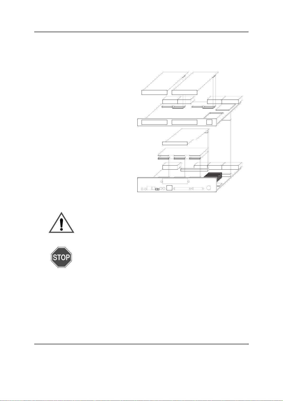
Figure 5 Schematic exploded mechanical construction view
The following figure is intended to get an overview over all available
main components of a SPARC/CPCI-52x(G).
2 PMC modules
I/O-52x(G)
UPA64S card
PMC Card PMC Card
PMC
PMC # 2 PMC # 1PMC # 1
PMC
Creator Graphic CardCreator Graphic Card
Memory Modules
EthernetEthernet
EthernetEthernet
Memory modules
UPA 64S
local PCI
Base-520(G)
MODEDIAG
RST
HLT
LED
MIC SPK
EthernetEthernet
UPA 64S
SCSI
SERIAL A + BSERIAL A + B
KBD
Caution The SPARC/CPCI-52x(G) is a sytem board. According to the Com-
pactPCI Specification PICMG 2.0 R2.1, the front panel of the
SP ARC/CPCI- 52x(G) sho ws a tr iangle . To ensure pr oper funct ioning
of the board, plug it exclusively in a system slot marked by a triangle.
Danger The Lithium battery of the RTC/NVRAM provides a data retention
of at least 7 years summing up all periods of actual battery use.
Therefore FORCE COMPUTERS assumes that there usually is no
need to exchange the Lithium battery except for example in the case
of long-term spare part handling.
Please observe the following:
• Exchange the battery before 7 years of actual battery use have
elapsed.
• Exchanging the battery always results in data loss of the devices
which use the battery as power backup. Therefore, back up
affected data before exchanging the battery.
• Always use the same type of Lithium battery as is already
installed.
SPARC/CPCI-52x(G) Page 13
Page 28

Installation Prerequisites and Requirements Installation
• Use appropriate tools to remove the battery.
• When installing the new battery ensure that the marked dot on
top of the battery covers the dot mark ed on the chip.
• Used batteries have to be disposed according to your country’s
legislation.
3.1 Installation Prerequisites and Requirements
Caution Before powering up check:
• this section for installation prerequisites and requirements
• and the consistency of the current switch setting (see section 4.4
“Switch Settings” on page 27).
3.1.1 Requirements
The installation requires at least
• a power supply
• a minimum airflow meeting the thermal requirements,
• and free CompactPCI backplane slots due to your
SPARC/CPCI-52x(G) variant:
– a system CompactPCI bus slot for the Base-520(G)
– an additional system CompactPCI bus slot for the IO-523G on the
right side of the Base-520(G)
– an additional system or peripheral CompactPCI bus slot for the IO-
522(G) on the right side of the Base-520(G).
Peripheral slot A peripheral slot of a CompactPCI rack is marked by a circle.
System slot A system slot of a CompactPCI rack is marked by a triangle.
Signaling level The SPARC/CPCI-52x(G) is a CompactPCI-universal board operational
in 3.3 V or 5 V CompactPCI systems. Therefore, no voltage keys are provided on the CompactPCI interface.
Power supply The power supply must meet the specifications given in the following ta-
ble. The values in the table below are maximum values without an
UPA64S card installed and without PMC modules.
Page 14 SPARC/CPCI-52x(G)
Page 29

Installation Installation Prerequisites and Requirements
T able 4 Maximum power supply values without UP A64S card and PMC modules
CPU board +5 V +3.3 V +/-12 V V I/O
SPARC/CPCI-520 6.5 A 4.6 A not required 200 mA
SPARC/CPCI-520G 6.5 A 4.6 A not required 200 mA
SPARC/CPCI-522 7.8 A 5.6 A not required 200 mA
SPARC/CPCI-522G 7.8 A 5.6 A not required 200 mA
SPARC/CPCI-523G 7.8 A 5.6 A not required 400 mA
Creator Graphic Card 1.3 A 2.2 A not required not required
Thermal
requirements
The operating temperature is 0 °C to +55 °C (humidity 5 % to 95 % noncondensing at +40 °C), when operating the SPARC/CPCI-52x(G) in systems providing a minimum forced airflow of 300 LFM (linear feet per
minute). The typical operating temperature of the system is 0 °C to
+40°C.
Table 5 Environmental requirements of the SPARC/CPCI-52x(G)
Operating Non-operating
Temperature 0 °C to +55 °C –40 °C to +85 °C
Forced air flow 300 LFM (linear feet per minute) –
Temp. change +/– 0.5 °C/min +/– 1 °C/min
Rel. humidity 5 % to 95 % noncondensing
at +40 °C
5 % to 95 % noncondensing
at +40 °C
Altitude –300 m to +3,000 m –300 m to +13,000 m
Audio interfaces Simultaneous use of the audio interfaces available on the front panel and
on the backplane can damage on-board hardware or connected devices.
For example: never us e t he hea dphone/line audio output at the backplane ,
if a headphone is plugged into the front-panel jack.
• Always use at most one of the interfaces if an audio interface is available on both the front panel and the backplane.
SPARC/CPCI-52x(G) Page 15
Page 30

Installation Prerequisites and Requirements Installation
Table 6 Audio interfaces requirements
Interface Description
Stereo Micro In
(op-amp pre-amp
with 18 dB gain)
• Signal level: single-ended condensator microphones with signal
level
–up to 12 mV with 20 dB gain inside Codec enabled
–and up to 120 mV with 20 dB gain inside Codec disabled
• Availability: on front panel and as factory option on backplane
instead of Aux#2 In
Stereo He adphone/ Line Out
• Signal level: maximum 2 V
designed to directly drive headphones)
line-level signal output (also
RMS
• Availability: on front panel and on backplane
Stereo Line In • Signal level: typical 47 kΩ audio input impedance; maximum full
scale input of 2 V
RM
• Availability: on backplane
Stereo Aux#1 In • Signal level: ~10 kΩ input impedance; maximum full scale input of
2V
RMS
• Availability: on backplane
Stereo Aux#2 In • Signal level: ~10 kΩ input impedance; maximum full scale input of
2V
RMS
• Availability: on backplane
Mono In • Signal level: typical 47 kΩ audio input impedance; nominally
1V
maximum (centered around 2.1 V) input signal level
RMS
• Availability : a s f ac tor y option on front panel i nstead of Micro In and
as factory option on backplane instead of Aux#1 In
Mono Out • Signal level depends on the setting of OLB which is a bit in the
Codecs Alternate Feature Enable I register (I16)
–maximum 1 V
–or maximum 0.707 V
output (centered around 2.1 V) if OLB = 1
RMS
(centered around 2.1 V) if OLB = 0
RMS
Default is OLB = 0.
• Availability: as factory option on backplane instead of Headphone/Line Out
Page 16 SPARC/CPCI-52x(G)
Page 31
Installation Installation Prerequisites and Requirements
3.1.2 Memory Modules
The main memory capacity is adjustable via installation of the appropriate memory modules.
The qualified memory module s depend on the SPARC/CPCI- 52x(G) pr ocessor frequency. They are given in the following table.
Table 7 Qualified memory modules
Processor frequency Memory modules
up to 300 MHz SPARC/MEM-50x
SPARC/MEM-50x-5
333 MHz and above SPARC/MEM-50x-5
Caution Do not install SPARC/MEM-50x and SPARC/MEM-50x-5 memory
modules on the same board, otherwise system malfunction may occur.
In the following it will be refered to all memory module types as
SPARC/MEM-50x.
The Base-520(G) can hold 1 to 4 memory modules providing up to
1 GByte DRAM capacity. 1 memory module can carry 2 memory banks.
Note: At least 1 lower memory module MEM-50L is required.
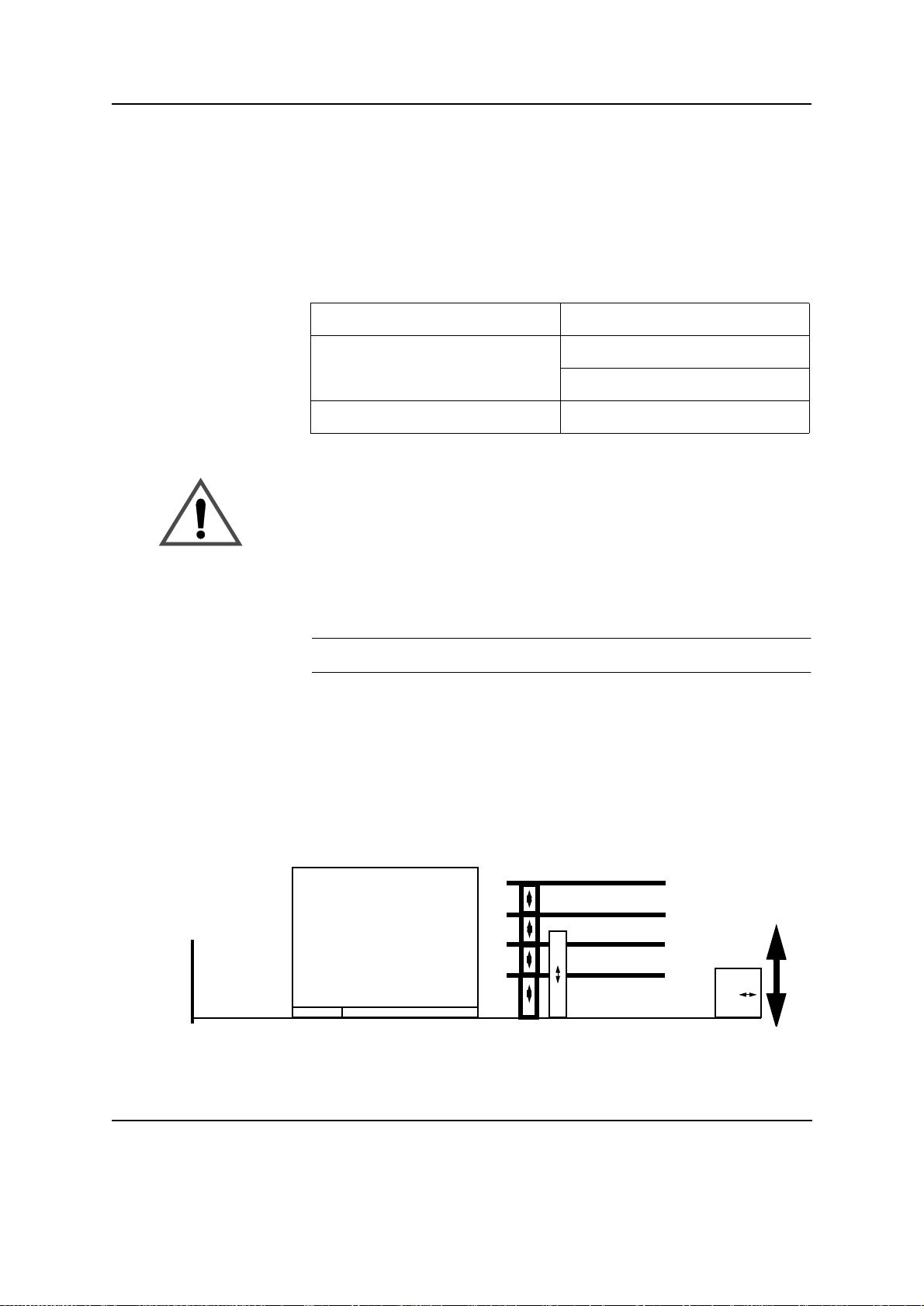
See the following figure for the memory module numbering scheme:
• Memory modules #1 and #2 are located in the first CompactPCI slot
the SPARC/CPCI-52x(G) occupies.
• Memory modules #3 and #4 are loc ated in the second Compa ctPCI sl ot
the SPARC/CPCI-52x(G) occupies.
Figure 6 MEM-50 – memory module numbering scheme
MEM-50 #4
MEM-50 #3
MEM-50 #2
MEM-50 #1
B
a
c
k
p
l
a
n
e
SPARC/CPCI-52x(G) Page 17
Page 32

Installation Prerequisites and Requirements Installation
The memory configuration is adjustable to the application’s needs via selection of the appropriate memory modules. The memory configuration
must fulfill the following requirements:
• The lowest memory module (#1) must be a SPARC/MEM-50L –
which is a lower memory module.
• The top memory module (with the greatest number in your configuration given the number scheme in the figure above) can be a
SPARC/MEM-50M or SPARC/MEM-50U – which is a middle (M)
or upper (U) memory module. The upper module misses the connectors for another memory module to be stacked on top.
• The memory modules between the lowest and the top memory module
must be SPARC/MEM-50M, i.e. middle memory modules.
• If a UPA64S card is installed, at most 2 memory modules can be
installed and memory module #2 must be a SPARC/MEM-50U, i.e.
an upper memory module.
• Note the limitations given by the SPARC/CPCI-52x(G) configuration
under consideration (see section 4.2 “Mechanical Construction” on
page 23).
Table 8 Qualified memory configurations (all data in MByte)
Total capacity 32 64 128 256 384 512 768 1024
Mem. modu le #4 –––––––256
Mem. modu le #3 – – – – – – 256 256
Mem. modu le #2 – – – – 128 256 256 256
Mem. modu le #1 32 64 128 256 256 256 256 256
3.1.3 Solaris Installation
Out of the extensive list of possible configurations the following memory
module configurations have been qualified (others may be tested and
qualified on request):
For installa tion information see t he respective Installation Guide deliv-
ered together with the memory module.
When installing Solaris, there are some general installation guidelines to
be followed before and during Solari s inst alla ti on and a s pecif ic guid el ine
related to S CSI to be followed afte r Solaris installatio n (see “SCSI” on
page 20).
Page 18 SPARC/CPCI-52x(G)
Page 33

Installation Installation Prerequisites and Requirements
General Installation Guideli nes
Note: Solaris versions and hardware updates prior to 2.5.1 11/97
and 2.6 03/98 are not supported.
Required
software
packages
Table 9 Required Solaris Packages
Table 10 Customizing Solaris
Software Group
Entire distribution plus
OEM support
In case of Solaris 2.5.1 and Solaris 2.6 the following Solaris software
packages must be installed, otherwise Solaris fails to boot.
Package Description
SUNWvplr.u
SUNWvplu.u
SMCC sun4u new platform links
SMCC sun4u new usr/platform links
When setting up Solaris interactively, these packages can be installed by
selecting the proper software group in the Software dialog. Customize
the software groups as follows:
Customization required for
Solaris 2.5.1 Solaris 2.6
No customization is required
Entire distribution Select the following clusters:
Developer system
• SMCC platform links
support
End user system support
Core system support
SPARC/CPCI-52x(G) Page 19
Page 34

Installation Prerequisites and Requirements Installation
SCSI
The Solaris SCSI driver may revert Wide-SCSI devices, which are connected to the front-panel SCSI connector, to asynchronous mode. However, it is possible to operate such a configuration in synchronous mode
also by inserting the following line into /kernel/drv/glm.conf:
n
target
-scsi-options=0x5f8
where n is the SCSI ID of the Wide-SCSI device under consideration. In
case of several Wide-SCSI devices insert the respective line per device.
Terminate the file with a ";".
3.1.4 Terminal connection
The SPARC/CPCI-52x(G) provides 2 serial interfaces (A and B) which
are implemented on the Base-520(G). For the initial power up, a terminal
can be connected to interface A via the front-panel 26-pin-MicroD-Sub
connector SERIAL A+B. Per default, all serial I/O interfaces provide an
RS-232 interface. As factory option the 2 interfaces can be configured as
RS-422 interface.
For information on the serial interface connector pinout, see section 4.5.4
“Serial I/O Interface Connector Pinout” on page 34.
Page 20 SPARC/CPCI-52x(G)
Page 35

Base-520(G) Installation Location Overview
4 Base-520(G) Installation
4.1 Location Ov erview
The Base-520(G) contains the following main components:
• a UltraSPARC-IIi processor,
• a second level cache (L2 cache),
• a CompactPCI interface,
• a boot PROM (PLCC),
• a boot flash EPROM (TSOP) and an user flash EPROM (TSOP),
• 3 connectors for the memory modules,
• a connector for interfacing to a UPA64S card,
• a connector for interfacing to the I/O-52x(G),
•switches,
• temperature sensors,
• and the fo llowing I/O interfa ces: SCSI # 1, Ethernet # 1, floppy, keyboard and mouse, audio, parallel i nterface as well as the 2 serial interfaces A+B.
SPARC/CPCI-52x(G) Page 21
Page 36
Location Overview Base-520(G) Installation
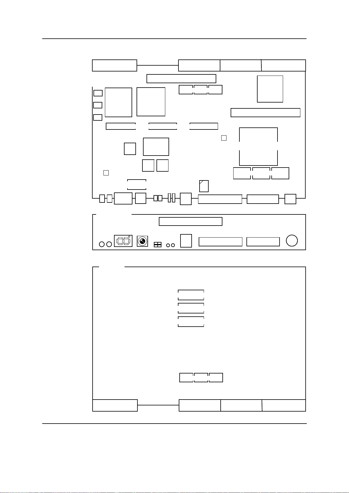
Figure 7 Location diagram of the Base-520(G) (schematic)
J1J5 J2J3
Top
SW4
SW5
Ethernet #1
SW6
Temperature
sensor #2
Front panel
RESET
2 slots high
UPA64S connector P7
SCSI #1
MEM-50L connectors P8, P9, P10
Audio
Super I/O
PHYceiver
Serial I/O
RTC/ NVRAM
DIA
G
MOD
E
RUN BM
ABORT
0 1
UPA64S-slot
MIC
HD
PH
XCVR
Temperature
sensor #1
Boot PROM (PLCC)
SCS
ETHERNET
APB
Connector for I/O board P6
UltraSPARC-IIi
L2 cache
I
SERIALA + B
KBD
Bottom
User flash EPROM #1 (TSOP)
Boot flash EPROM (TSOP)
User flash EPROM #2 (TSOP) assembly option
XCVR
J1J5 J2J3
Page 22 SPARC/CPCI-52x(G)
Page 37
Base-520(G) Installation Mechanical Construction
4.2 Mechanical Construction
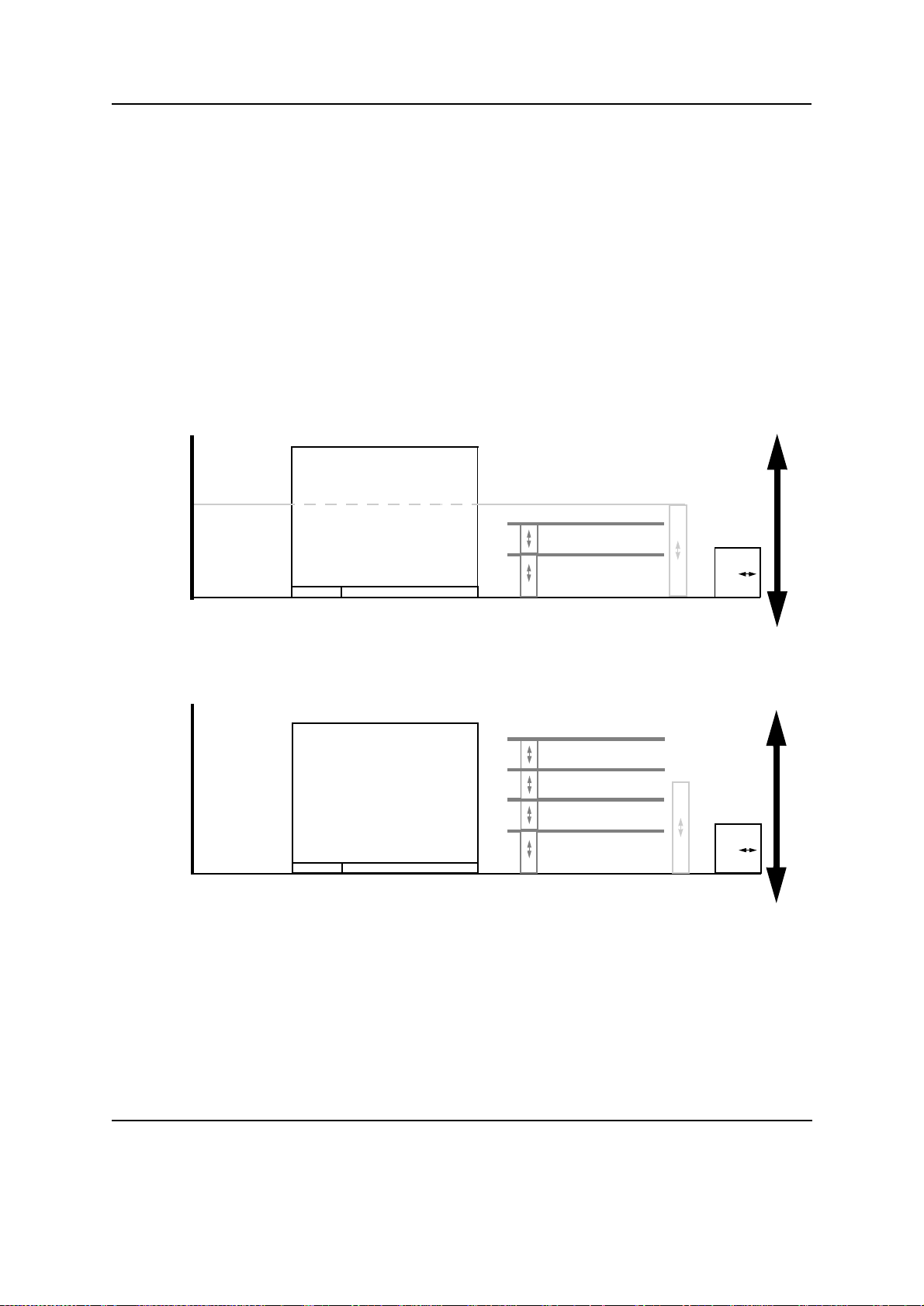
The Base-520(G) is a CompactPCI computer. It occupies 2 CompactPCI
slots and consists of the following major components:
• an I/O connector for the I/O-52x(G),
• an UPA64S connector for an UPA64S card (only Base-520G),
• 3 memory module connectors for up to 4 memory modules. With an
installed UPA64S card only 2 memory modules are possible.
The following figures show the Base-520(G) in possible configurations :
Figure 8 Mechanical construction of a Base-520G
F
r
FORCE
o
COMPUTERS
n
UPA64S card
t
p
a
n
e
Base-520G
l
in 1st slot
CPU and cache with
heatsink
MEM-50U
MEM-50L
B
a
c
k
p
l
a
n
e
Figure 9 Mechanical construction of a Base-520G with 4 memory modules
F
r
o
n
t
p
a
n
e
l
CPU and cache with
heatsink
Base-520G
in 1st slot
MEM-50U
MEM-50M
MEM-50M
MEM-50L
B
a
c
k
p
l
a
n
e
SPARC/CPCI-52x(G) Page 23
Page 38
Mechanical Construction Base-520(G) Installation
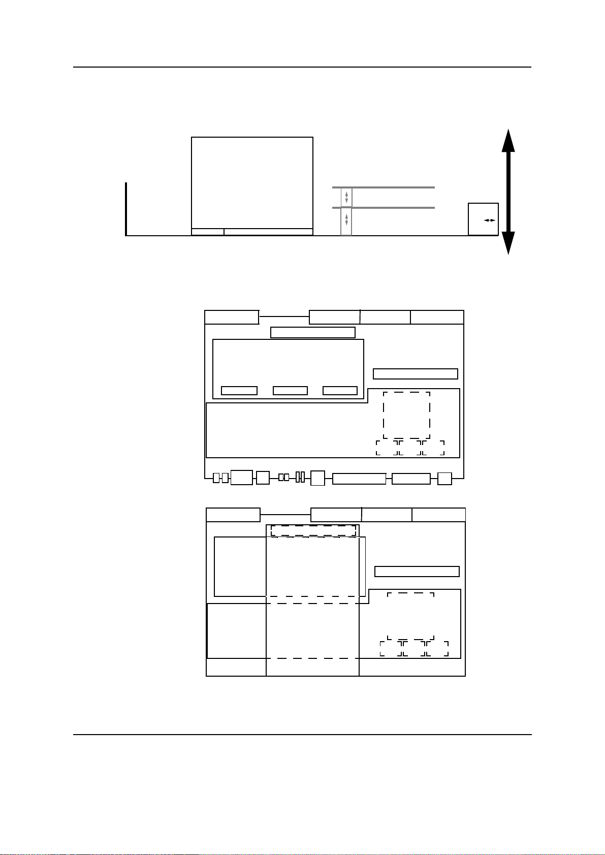
Figure 10 Mechanical construction of a Base-520
F
r
o
n
t
p
a
n
e
Base-520 in
l
1st slot
CPU and cache with
heatsink
MEM-50U
MEM-50L
B
a
c
k
p
l
a
n
e
The Base-520 is only available as a 2-slot solution with an I/O-522.
Figure 11 Components of a 2-slot configuration with UPA64S card (schematic)
J1J5 J2J3
➤ UPA64S card
1st of 2 slots
Base-520G with up
to 2 memory
modules
2nd of 2 slots
UPA64S card
Up to 2 memory modules
➤ Memory modules
Heat sink for CPU and cache
➤ Base-520G
Memory
modules
UPA64S card
➤ I/O-52xG
J1J5 J2J3
➤ I/O-52xG
Heat sink for
CPU and cache
Page 24 SPARC/CPCI-52x(G)
Page 39

Base-520(G) Installation Mechanical Construction
4.2.1 FORCE COMPUTERS UPA64S Card Installation
You can only install a FORCE COMPUTERS UPA64S card if you purchased a SPARC/CPCI-52xG version. It is connected to the Base-520G
via the UPA64S connector P7 (see figure 7 “Location diagram of the
Base-520(G) (schematic)” on page 22).
Note: Use only UPA64S cards from FORCE COMPUTERS.
Throughout this section the term “UPA64S card” always refers to a
card purchased from FORCE COMPUTERS and specified for use
with a SPARC/CPCI-52xG.
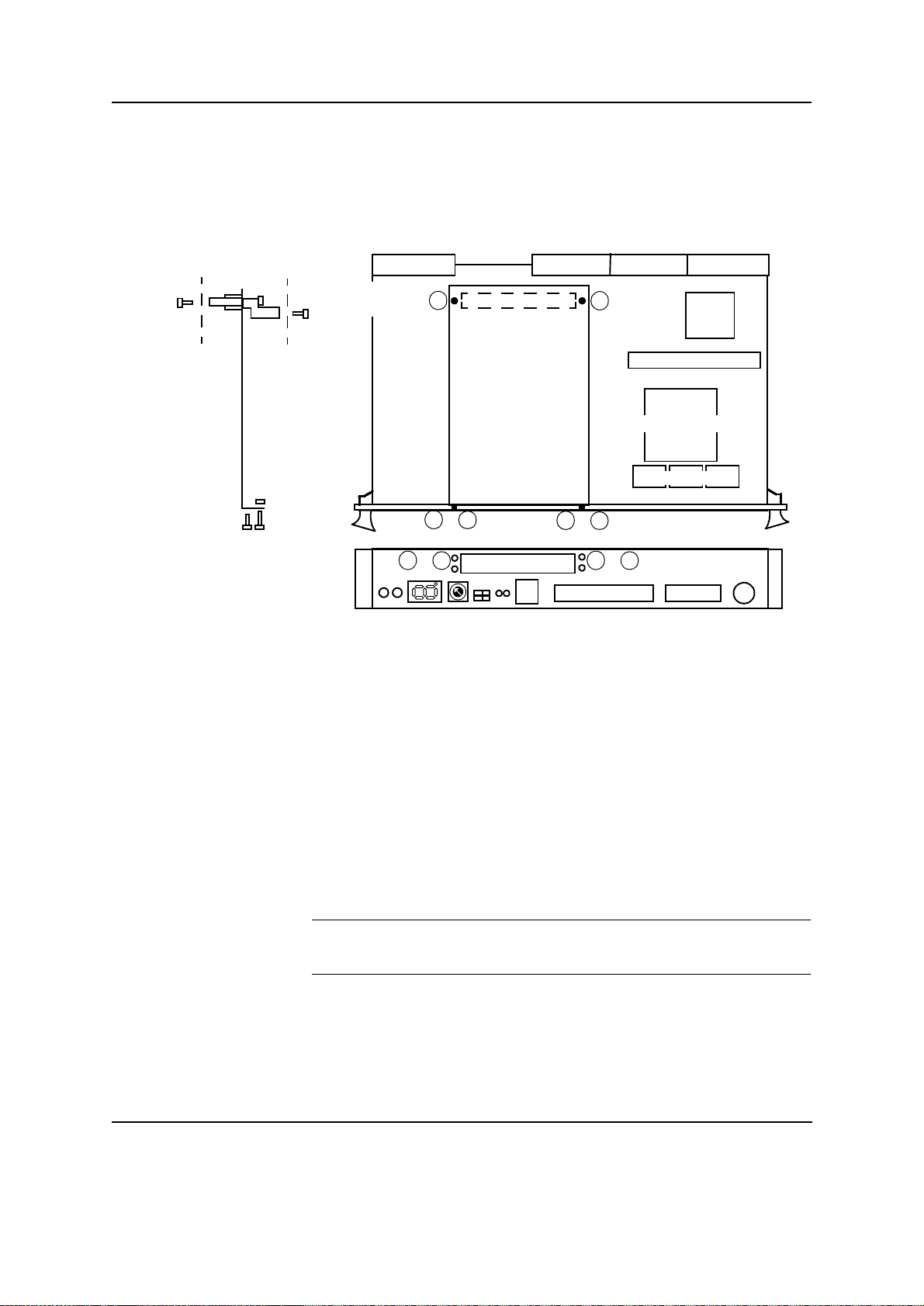
For the locations mentioned in the description see figure 12 “Installing/Deinstalling an UPA64S card” on page 26.
Installation of a
UPA64S card
1. If an I/O-52xG is installed, remove it as described in the I/O-52x(G)
installation section. Remove the 2 z-standoffs at location 5 and 6
from the Base-520G by loosi ng the res pec tive 2 sc rews. Keep them in
a save place to have them available for reusing the I/O-52xG without
UPA64S card.
2. If you do not install an I/O-52xG afterwards: Remove the 2 z-standoffs fixed on the UPA64S card by loosing the respective 2 screws and
fix the UPA64S card again with 2 of the 4 shorter screws delivered
with the UPA64S card on the 2 standoffs which connect it to the
Base-520G.
3. Remove the blind panel fixed in the UPA64S front panel slot. Store it
in a safe place for later us e.
4. Plug the prepared UPA64S card from FORCE COMPUTERS to the
respective UPA64S connector on the Base-520G.
5. Fix the UPA64S card with 2 of the 4 short screws at location 5 and 6
on the bottom side of t he Base-520G and with the 4 screws and 2 n uts
from the blind panel on the front panel at location 1...4.
Now the UPA64S card is installed.
6. If an I/O-52xG was installed, fix it again as described in the
I/O-52x(G) installation section.
Uninstalling a
UPA64S card
1. If an I/O-52xG is installed, remove it as described in the I/O-52x(G)
installation section.
2. Remove the 4 screws and 2 nuts on the front panel at location 1...4.
Remove the 2 screws at location 5 and 6 on the bottom side of the
Base-520G.
3. Remove the UPA64S card by lifting it.
SPARC/CPCI-52x(G) Page 25
Page 40
Powering Up Base-520(G) Installation
4. If you do not install the UPA 64S card again, fix the blind panel.
5. To install the I/O-52xG again refer to the installation section of the
I/O-52x(G).
Figure 12 Installing/Deinstalling an UPA64S card
UPA64S
card
Base-520G
I/O-52xG
4.3 Powering Up
Top
J1J5 J2J3
5
UPA64S card
21
&
2
1
&
UPA64S slot
6
I/O-52xG connector
UltraSPARC-IIi
4
3
&
4
3
&
APB
L2 cache
The initial powering up can be done by connecting a terminal to the front
panel serial I/O inter fac e A. The advantage of using a terminal is that you
do not need any frame buffer, monitor, or keyboard for initial powering
up.
Booting The SPARC/CPCI-52x(G) boot PROM consists of a 1 MByte PROM
(OTP) PLCC socket device (not writeable). Alternatively a 2 MByte
TSOP boot flash EPROM device can be enabled by SW6-2. This boot
flash EPROM device is writeable if enabled by SW4-3.
Note: If you have an unformatted floppy disk in a floppy connected
to your SPARC/CPCI-52x(G) then the OpenBoot does not come up.
Per default the SPARC/CPCI-52x(G) is shipped with its boot PROM
containing the OpenBoot firmware (see section 4.8 “OpenBoot Firm-
ware” on page 42).
Page 26 SPARC/CPCI-52x(G)
Page 41
Base-520(G) Installation Switch Settings
ON
1
2
3
4
User application The SPARC/CPCI-52x(G) provid es 1 user flash EPROM devices (2M*8)
to store user applications. As factory option 2 user flash EPROM devices
(2M*8) are possible. For write-protection of the user flash EPROM see
SW4-4 in section 4.4 “Switch Settings” on page 27.
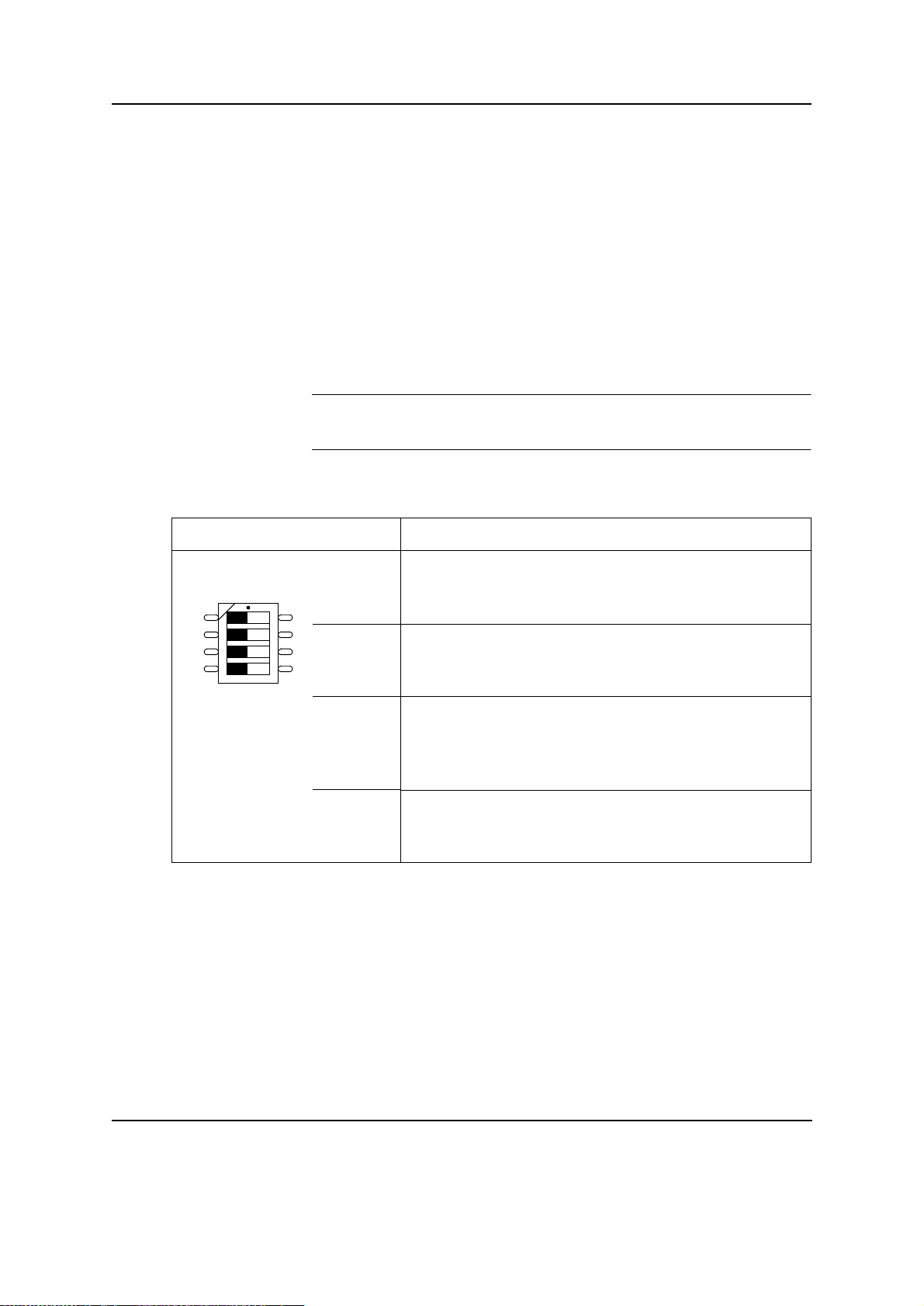
4.4 Switch Settings
The following table lists the functions and the default settings of all
switches shown in figure 7 “Location diagram of the Base-520(G) (schematic)” on page 22.
Note: Before powering up the board check the current switch
settings for consistency. Do not switch during operation.
Table 11 Default switch settings
Name and default setting Function
SW4-1
OFF
SW4-2
OFF
SW4-3
OFF
SW4-4
OFF
Reset key on front-panel control
OFF = RESET key enabled
ON = RESET key disabled
Abort key control
OFF = ABORT key enabled
ON = ABORT key disabled
Boot flash EPROM write protection
(only relevant if SW6-2 = ON)
OFF = boot flash EPROM write protected
ON = boot flash EPROM write enabled
User flash EPROM write protection
OFF = user flash EPROM write protected
ON = user flash EPROM write enabled
SPARC/CPCI-52x(G) Page 27
Page 42
Front Panel and Connectors Base-520(G) Installation
ON
1
2
3
4
ON
1
2
3
4
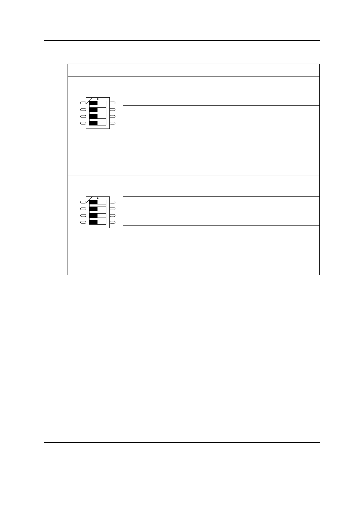
Table 11 Default s witch settings (cont.)
Name and default setting Function
SW5-1
OFF
SW5-2
OFF
SW5-3
OFF
SW5-4
OFF
SW6-1
OFF
SW6-2
OFF
SW6-3
OFF
SW6-4
OFF
SCSI term ination for SCSI #1 on front panel
OFF = front panel term ination autom atic
ON = front panel termination disabled
SCSI termination for SC SI #1 on bac kplane
OFF = backplane termination disabled
ON = backplane termination enabled
Reserved, must be OFF
Reserved, must be OFF
Reserved, must be OFF
Select boot device
OFF = boot from boot PROM
ON = boot from boot flash EPROM
Reserved, must be OFF
Watchdog enable switch
OFF = disabled
ON = enabled
4.5 Front Panel and Connectors
Front panel
features
Page 28 SPARC/CPCI-52x(G)
The features of the front panel are described in the following table. For a
location diagram see figure 7 “Location diagram of the Base-520(G)
(schematic)” on page 22.
Page 43

Base-520(G) Installation Front Panel and Connectors
Table 12 Front panel features
Device Description
RESET Mechanical reset key:
When enabled and toggled it instantaneously affects
the SPARC/CPCI-52x(G) by generating a push-button Power On Reset (POR) to the UltraSPARC-IIi.
Push-button Power On Reset has the same effect as a
Power On Reset from the power supply, with the only
difference, that the corresponding status bit (B_POR)
in the UltraSPA RC - IIi Reset_Control Register is
set and the DRAM refresh is not influenced.
For information on disabling the reset key,
see “SW4-1” on page 27.
ABORT Mechanical abort key:
When enabled and toggled it instantaneously affects
the SPARC/CPCI-52x(G) by generating a push-button externa l initiated reset (X IR). Push-button e xternal initiated reset allows a user-reset (abort) of part of
the processor without resetting the whole system.
UltraSPARC-IIi sets the B_XIR bit in the
Reset_Control Register when a push-button external initiated reset i s detected.
For information on disabling the abort key, see
“SW4-2” on page 27.
DIAG Software programmable hexadecimal display for di-
agnostics.
MODE Hexadecimal rotary switch, decoded with 4 bit. De-
fault settin g: F
16
.
RUN CPU status LED:
green
normal operation
red
the processor is halted or reset is active;
it starts blinking to signal that the processor did not
access the PCI bus for more than 1 second.
BM CompactPCI busmaster LED:
green
if the SPARC/CPCI-52x(G) accesses the CompactPCI as master
off
otherwise
SPARC/CPCI-52x(G) Page 29
Page 44

Front Panel and Connectors Base-520(G) Installation
Table 12 Front panel features (cont.)
Device Description
0, 1 2 software programmable user LEDs.
Possible status: off, red, yellow, or green, all colors
either permanent or with a blinking frequency of ap-
proximately 0.5, 1, or 2 Hz.
MIC Standard 3.5 mm microphone jack
HDP H Standard 3.5 mm headphone jack
ETHERNET Standard Twisted-Pair-Ethernet RJ45 connector for
10BaseT/100BaseTX Ethernet.
SCSI 50-pin shielded fine-pit ch connect or for sta ndard SCSI
SERIAL A+B 26-pin shielded fine-pitch connector for 2 serial inter-
faces
KBD Standard 8-pin mini-DIN connector for keyboard and
mouse
On-board
connectors
In addition to the front-panel connectors, the Base-520(G) provides onboard connectors for memory modules and for the I/O-52x(G), only the
Base-520G provides the UPA64S interface connector. An overview of
the on-board connectors is shown in the following table.
Table 13 On-board connectors
Connector description and loc at ion Connector type
CompactPCI backplane connector
J1, J2, J5
I/O-52x(G) connector P6 100-pin MBus connector
UPA64S interface connector P7 120-pin UPA connector fe-
Memory module connectors
P8, P9, P10
Available
interfaces on J5
The following list shows the ava ilabl e inte rfac es on the J5 backpla ne con-
nector. For the J5 connector pinout see Figure 13, “CompactPCI J5 connector pinout,” on page 36.
Standard Co mpactPC I metric,
5 row shielded connectors female
male
male
80-pin SMD connector
• Ultra Wide SCSI #1
• MII #1 Ethernet interface
Page 30 SPARC/CPCI-52x(G)
Page 45
Base-520(G) Installation Front Panel and Connectors
• Floppy interface
• Parallel interface
• Serial interface A and B
• Keyboard and mouse
• Audio In:
Stereo Line In,
Stereo Aux#1 In,
Stereo Aux#2 In (or Microphone In as factory option)
• Audio Out:
Stereo Line Out
4.5.1 Audio Interface
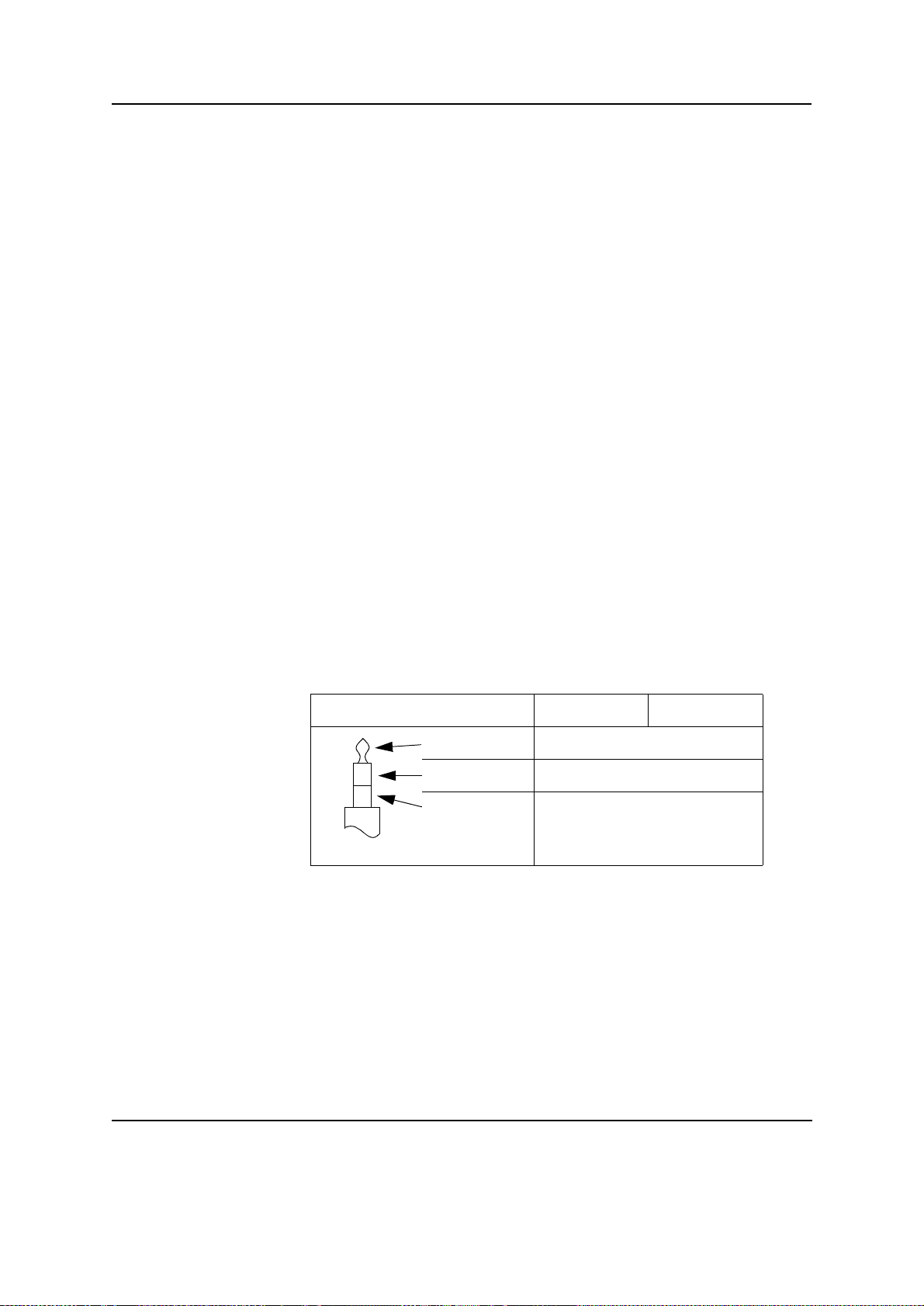
The 2 front panel audio interfaces use standard 3.5-mm-phono jacks supporting
• 1 single-ended condenser microphone
• 1 line level signal output, also designed to directly drive low impedance headphones
Table 14 Audio i nterface si gnals
Connector Headphone Microphone
Tip Left channel
Ring Right channel
Shield Analog GND
SPARC/CPCI-52x(G) Page 31
Page 46
Front Panel and Connectors Base-520(G) Installation
4.5.2 Ethernet Interfaces
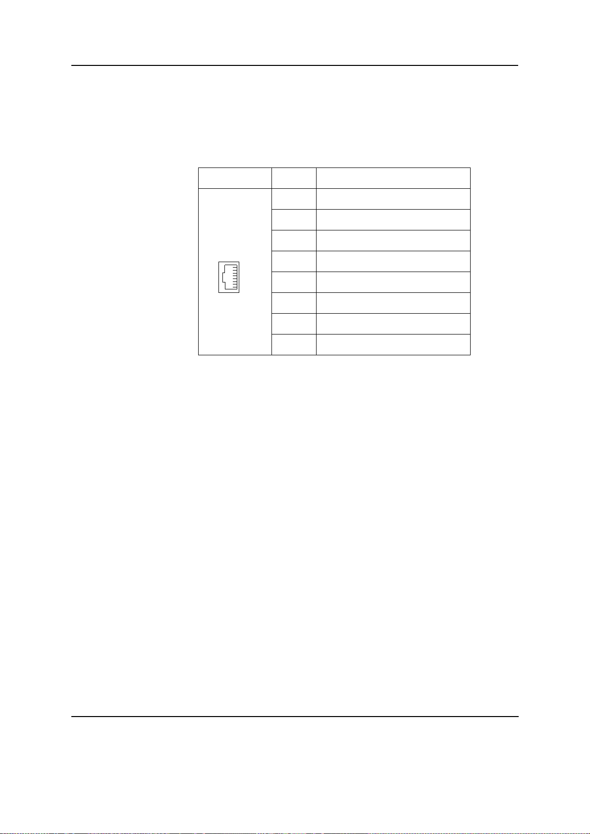
The full duplex Ethernet interface is available at the front panel via a
10BaseT/100BaseTx Twisted-Pair-Ethernet connector.
Table 15 Twisted-Pair-Ethernet #1 connector pinout
Connector Pin Signal
1TX+
2TX–
RJ-45 TPE
1
8
3RX+
4GND
5GND
6RX–
7GND
8GND
The Ethernet #1 interface i s als o ac cessi ble at the J5 back pan el conn ector
via an MII #1 interface.
If Ethernet #1 gets accessed via I/O panel, the
front panel connector is normally disabled automatically, for other configurations see the respective jumper settings in the SPARC/IOBP-520
Installati o n Gui de. For the J5 connector pinout see Figure 13, “Compact-
PCI J5 connector pinout,” on page 36.
Page 32 SPARC/CPCI-52x(G)
Page 47
Base-520(G) Installation Front Panel and Connectors
4.5.3 SCSI #1 Connector Pinout
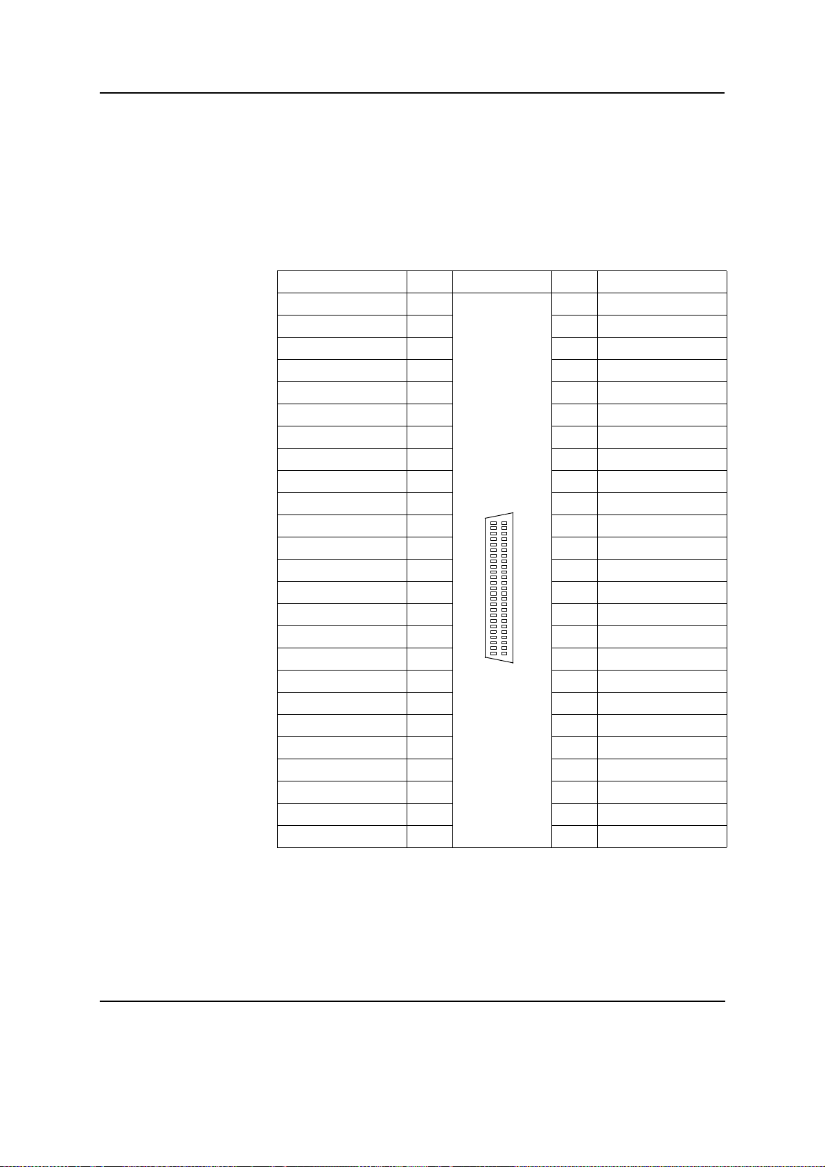
TERMPWR The SCSI #1 interface is single-ended and supports TERMPWR.
AUTOTERM Automatic termination mode means the respective termination is disabled
when you connect a standard SCSI cable to the front panel connector.
Table 16 50-pin SCSI connector pinout
Signal Pin Connector Pin Signal
GND 1 26 D0
GND 2 27 D1
GND 3 28 D2
GND 4 29 D3
GND 5 30 D4
GND 6 31 D5
GND 7 32 D6
GND 8 33 D7
GND 9 34 DP0
GND 10 35 GND
GND 11 36 AUTOTERM
50
25
n.c. 12 37 n.c.
n.c. 13 38 TERMPWR
n.c. 14 39 n.c.
GND 15 40 GND
GND 16 41 ATN
GND 17 42 GND
26
1
GND 18 43 BSY
GND 19 44 ACK
GND 20 45 RST
GND 21 46 MSG
GND 22 47 SEL
GND 23 48 CD
GND 24 49 REQ
GND 25 50 IO
SPARC/CPCI-52x(G) Page 33
Page 48
Front Panel and Connectors Base-520(G) Installation
4.5.4 Serial I/O Interface Connector Pinout
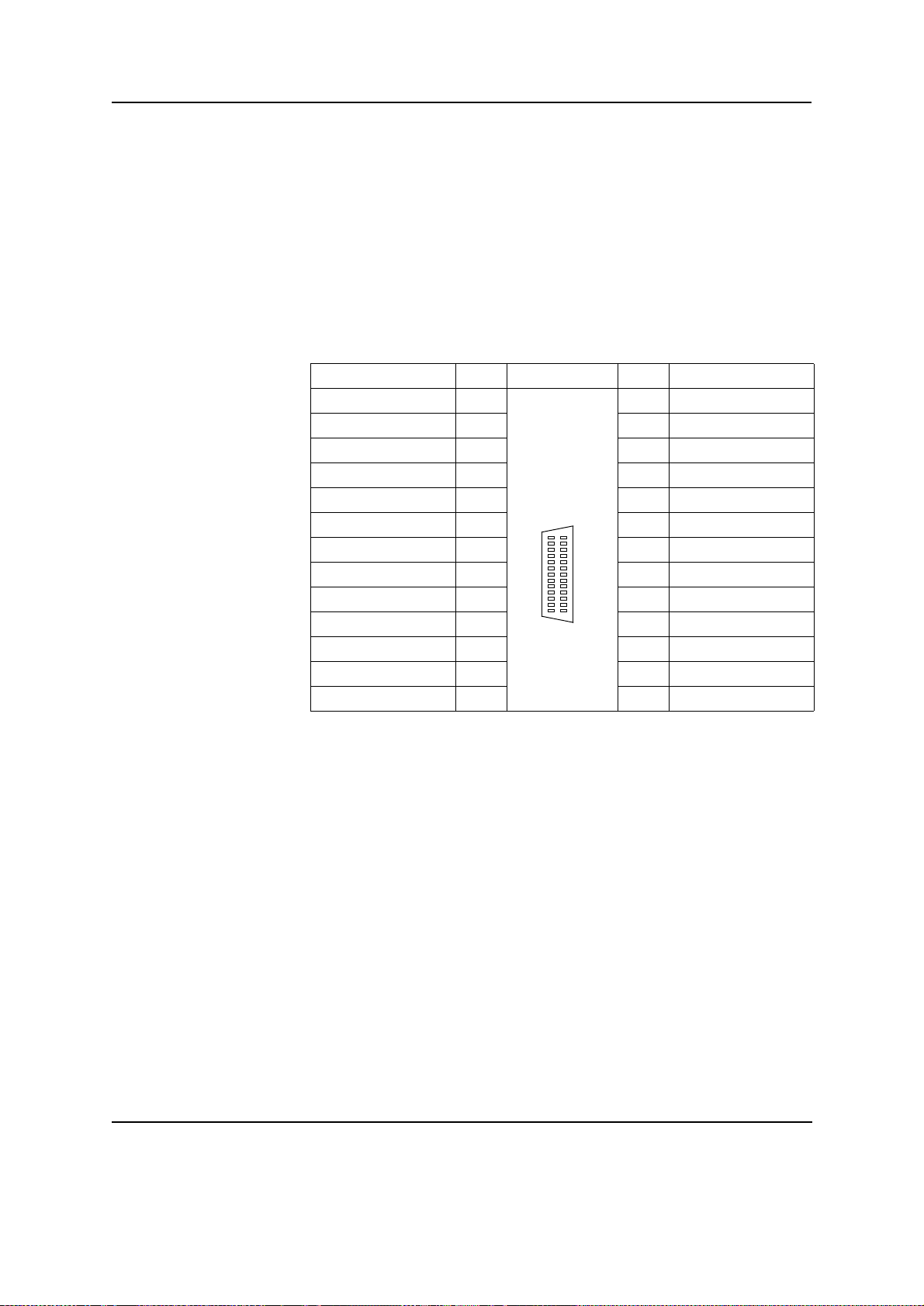
Both serial I/O interfaces of the Base-520(G) are independent full-duplex
channels. For each of them the 4 signals RXD, TXD, RTS, and CTS are
also provided via the respective CompactPCI J5 connector (for interface
A and B see figure 13 “CompactPCI J5 connector pinout” on page 36).
SERIAL A+B on the Base-520(G)’s front panel holds the signals for the
2 serial interfaces A and B.
Table 17 26-pin serial A+B connector pinout RS232
Signal Pin Connector Pin Signal
n.c. 1 14 TxD_B (Output)
TxD_A (Output) 2 15 RxC_A (Input)
RxD_A (Input) 3 16 RxD_B (Input)
RTS_A (Output) 4 17 RTxC_A (Input)
CTS_A (Input) 5 18 RxC_B (Input)
DSR_A (Input) 6 19 RTS_B (Output)
26
13
GND_A (Ground) 7 20 DTR_A (Output)
DCD_A (Input) 8 21 DSR_B (Input)
n.c. 9 22 RTxC_B (Input)
n.c. 10 23 GND_B (Ground)
14
1
DTR_B (Output) 11 24 TxC_A (Output)
DCD_B (Input) 12 25 TxC_B (Output)
CTS_B (Input) 13 26 n.c.
SERIAL A+B on the Base-520(G)’s front panel holds the signals for the
2 serial interfaces A and B.
Page 34 SPARC/CPCI-52x(G)
Page 49
Base-520(G) Installation Front Panel and Connectors
Table 18 26-pin serial A+B connector pinout RS422 (factory option)
Signal Pin Connector Pin Signal
n.c. 1 14 CTS+_B (Input))
CTS+_A (Input)) 2 15 nc
RTS–_A (Output) 3 16 RTS–_B (Output)
RTS+_A (Output) 4 17 nc
CTS–_A (Input) 5 18 nc
nc 6 19 RTS+_B (Output)
26
13
RxD–_A (Input) 7 20 RxD+_A (Input)
TxD–_A (Output) 8 21 nc
n.c. 9 22 nc
n.c. 10 23 RxD–_B (Input)
14
1
RxD+_B (Input) 11 24 TxD+_A (Output)
TxD–_B (Output) 12 25 TxD+_B (Output)
CTS–_B (Input) 13 26 n.c.
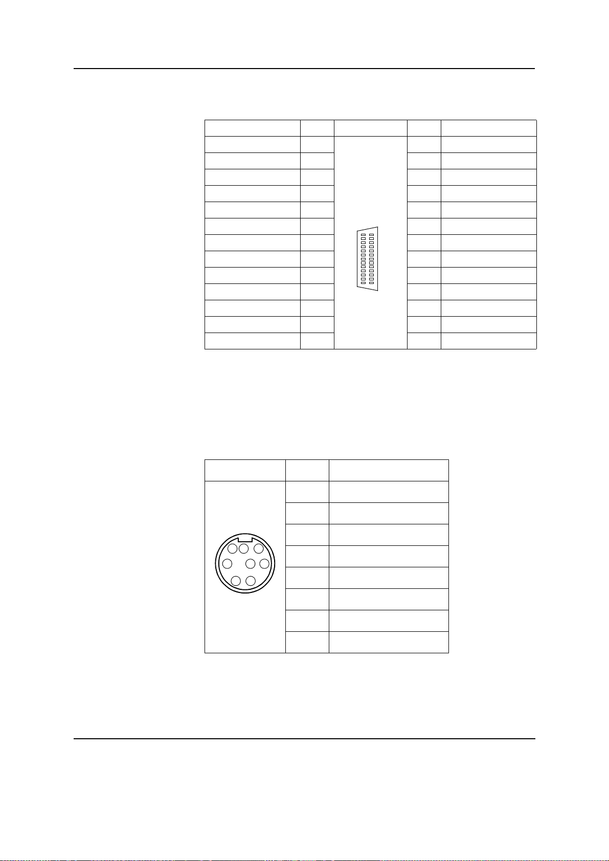
4.5.5 Keyboard/Mouse Connector
The SUN-type keyboard/mouse interface is available at the front panel
via an 8-pin mini-DIN connector.
Table 19 Keyboard/mouse connector pinout
Connector Pin Function
8 7 6
2 1
1GND
2GND
3+5V DC
4 35
4 Mouse In
5 Keyboard Out
6 Keyboard In
7 Mouse Out
8+5V DC
SPARC/CPCI-52x(G) Page 35
Page 50
Front Panel and Connectors Base-520(G) Installation
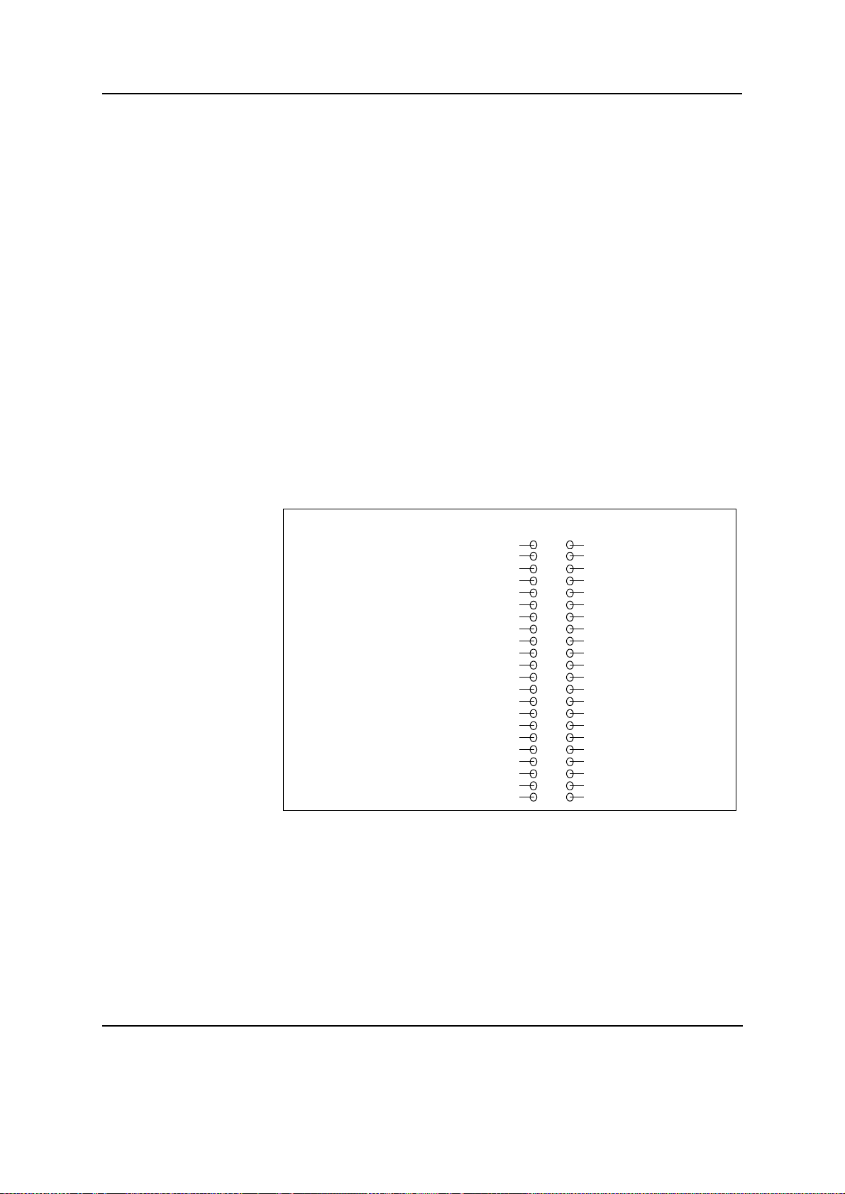
4.5.6 CompactPCI Backplane Connector Pinout
J1 and J2 The J1 and J2 connectors implement the CompactPCI 64-bit connector
pinout as specified by the CompactPCI Specificatio n. Ther ef ore , thi s se ction only documents the pinout of the J5 connector.
J3 J3 is reserved.
J5 Besides the CompactPCI specific pinout the following interfaces are
available on the CompactPCI J5 connector (the names used in the foll owing pinout is given in brackets):
SCSI (SCSI), MII (MII), parallel (LPT), floppy (FDC), serial interface
A (SerA), serial interface B (SerB), audio (AUD), keyboard (KBD),
mouse (MSE), fused 5 V power for the I/O panel (VP5).
The pinout shown in the figure below applies to RS-232 configuration of
the Base-520(G)’s serial I/O interfaces. Serial I/O interfaces configured
for RS-422 (factory option) are only available via the front panel connector.
Figure 13 CompactPCI J5 connector pinout
BA
Audio factory
option
SCSI #1 D8
SCSI #1 SEL
SCSI #1 ATN
SCSI #1 D4
SCSI #1 D0
SCSI #1 D12
MII #1 RXD3
MII #1 RX_DV
MII #1 TXD3
FDC HDSEL
FDC WDATA
FDC DR0
FDC EJECT
LPT BSY
VP5_IOBP
LPT D4
LPT D0
SerA RXD
SerA TXD
SerA DTR
AUD RLINEIN
AUD LLINEIN
SCSI #1 D9
SCSI #1 CD
SCSI #1 BSY
SCSI #1 D5
SCSI #1 D1
SCSI #1 D13
MII #1 RXD2
MII #1 COL
MII #1 TXD2
FDC DSKCHG
FDC WGATE
FDC DR1
FDC DENSEL
LPT ERR
LPT PE
LPT D5
LPT D1
SerA CTS
SerA RTS
KBD DOUT
AUD RAUX2IN
AUD LAUX2IN
As factory option the following signals are routed to the mentioned pins
instead of the signals mentioned in the connector pinout above:
SCSI #1 D10
SCSI #1 REQ
SCSI #1 ACK
SCSI #1 D6
SCSI #1 D2
SCSI #1 D14
MII #1 RXD1
MII #1 CRS
MII #1 TXD1
MII #1 TX_EN
FDC TRK0
FDC MTR0
FDC DSENS
LPT SLIN
LPT SLCT
LPT D6
LPT D2
SerB DCD
SerA DCD
KBD DIN
AUD RAUX1IN
AUD LAUX1IN
• Pin 21 row C: AUD MIN (Mono In)
1
2
3
4
5
6
7
8
9
10
11
12
13
14
15
16
17
18
19
20
21
22
DC
SCSI #1 D11
SCSI #1 IO
SCSI #1 RST
SCSI #1 D7
SCSI #1 D3
SCSI #1 D15
MII #1 RXD0
MII #1 RX_ER
MII #1 TXD0
MII #1 TX_ER
FDC WP
FDC DIR
FDC INDEX
LPT INIT
LPT AFD
LPT D7
LPT D3
SerB CTS
SerB RTS
MSE DIN
AUD ROUT
AUD LOUT
E
n.c.
WIDETERMPWR
SCSI #1 MSG
TERMPWR
SCSI #1 DP0
SCSI #1 DP1
MII #1 RX_CLK
MII #1 MGT_DIO
MII #1 TX_CLK
MII #1 MGT_CLK
FDC RDATA
FDC STEP
VP5_IOBP
n.c.
n.c.
LPT ACK
LPT STB
SerB RXD
SerB TXD
SerB DTR
AUD MOUT
AUD AGND
• Pin 21 row B: AUD RMICIN (Right Micro In)
• Pin 22 row B: AUD LMICIN (Left Micro In)
Page 36 SPARC/CPCI-52x(G)
Page 51

Base-520(G) Installation Front Panel and Connectors
I/O panel As a separate price list item an I/O panel is available for the Base-520(G),
the SPARC/IOBP-520/CPU. An extended variant is the SPARC/CPCI520/AccKit/CPU which contains additionally to the I/O panel the following cables:
–a serial splitter cable for the front panel and the I/O panel
–a flat ribbon SCSI cable for the I/O panel
–a Micro D-Sub SCSI cable for the front panel
–and a Twisted-Pair-Eth ernet cable for the front panel or I/O panel.
The I/O panel supports the following interfaces:
• Fast/Wide SCSI #1,
• MII #1 Ethernet,
• Serial A/B interface,
• Audio interface,
• Keyboard/Mouse,
• Parallel i nterface,
• and Floppy interface.
Danger The SPARC/IOBP-520/CPU and the SPARC/CPCI-520/AccKit/CPU
is especially designed for the Base-520(G). Do not use any other I/O
panels on the Base-520(G).
Use only the front panel or the backpanel Ethernet interface, not
both. Check the configuration of your I/O panel.
All switches on the Base-520(G) concerning the SCSI-bus termination must be configured so, that the corresponding backplane terminator (SW5-2) is disabled! This is necessary as the I/O panel includes
automatic termination for the backplane SCSI-bus.
SPARC/CPCI-52x(G) Page 37
Page 52

SCSI #1 Configuration Base-520(G) Installation
4.6 SCSI #1 Configura tion
Note: Correct SCSI bus selection: The Base-5 20(G) provi des 1 SCSI
bus, SCSI #1. A further SCSI controller, SCSI #2, is available with
the I/O-52x(G). Its termination is described in the I/O-52x(G)
installation section.
SCSI #1
termination
The Base-520(G)’s SCSI #1 bus is accessible via the Base-520(G)’s
front-panel SCSI #1 connector (8-bit SCSI) and via the Base-520(G)’s J5
connector (Wide SCSI). Therefore, the Base-520(G) holds 2 distinct
SCSI bus terminations to enable correct termination of the SCSI #1 bus.
Associated to the 2 terminations there are 2 switches – SW5-1 and
SW5-2 – which allow easy selection of a valid SCSI #1 bus configuration.
There are 4 valid Base-520(G) switch settings corresponding to valid
SCSI #1 bus configurations. The following factors differentiate the valid
SCSI #1 bus configurations:
• the Base-520(G)’s location within the SCSI #1 bus: Is the
Base-520(G) located at an endpoint of the SCSI #1 bus?
• the connector(s) being used from the SCSI #1 bus:
– Is a SCSI cable plugged into the Base-520(G)’s front-panel SCSI
connector?
– Is the Base-520(G)’s CompactPCI J5 connector used by the
SCSI #1 bus?
– Are both Base-520(G) connectors used by the SCSI #1 bus?
• the SCSI device type being connected to the SCSI #1 bus: Is a WideSCSI device connected to the J5 connector?
Each of the following configuration descriptions starts with identifying
the SCSI #1 bus configuration being covered and ends with defining the
correct switch setting corresponding to the configuration under consideration.
Page 38 SPARC/CPCI-52x(G)
Page 53
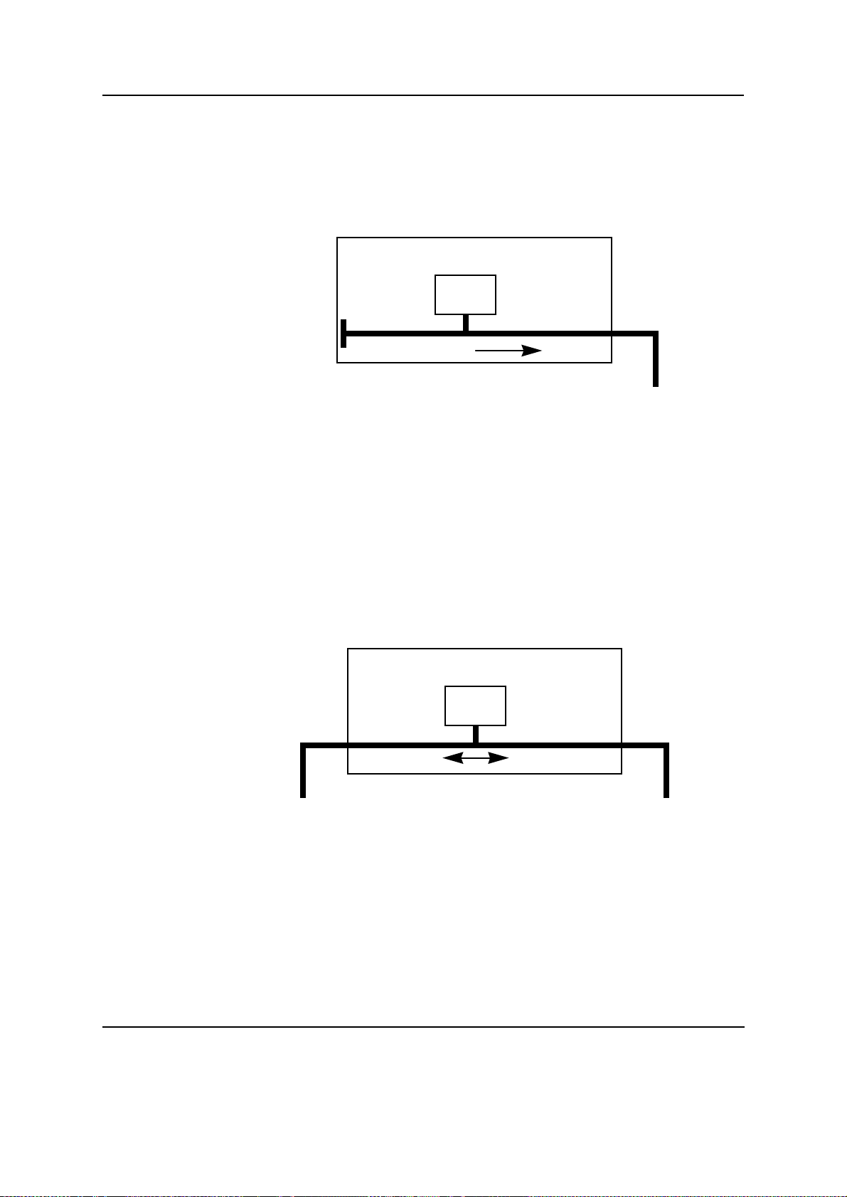
Base-520(G) Installation SCSI #1 Configuration
Default
configuration 1
for 8 bit SCSI
• The default configuration 1 is covered by the default switch setting:
The Base-520(G) is located at an endpoint of the SCSI #1 bus, the
SCSI #1 bus is extended via the CompactPCI backplane (J5 connector), but no SCSI cable is plugged into the front-panel SCSI connector:
Front
panel
SW5-1 = OFF SW5-2 = OFF
No SCSI cable
plugged in
Base-520(G)
SCSI #1
controller
Endpoint of
SCSI #1 bus
CompactPCI
backplane
In this configuration (default switch setting):
– SW5-1 must be set to OFF = front panel termination automatic
(automatic enabling or disabl ing of te rminati on by sensi ng whet her
a SCSI cable is plugged in)
– and SW5-2 must be set to OFF = backplane termination disabled.
Default
configuration 2
for 8 bit SCSI
• The default configuration 2 is also covered by the default switch setting: the Base-520(G) is not located at an endpoint of the SCSI #1
bus, the SCSI 1 bus is extended via the CompactPCI backplane and
via the front-panel SCSI connector:
Front
panel
SW5-1 = OFF
SCSI cable
plugged in
Base-520(G)
SCSI #1
controller
SW5-2 = OFF
CompactPCI
backplane
In this configuration (default switch setting):
– SW5-1 must be set to OFF = front panel termination automatic
(automatic enabling or disabl ing of te rminati on by sensi ng whet her
a SCSI cable is plugged in)
– and SW5-2 must be set to OFF = backplane termination disabled.
SPARC/CPCI-52x(G) Page 39
Page 54
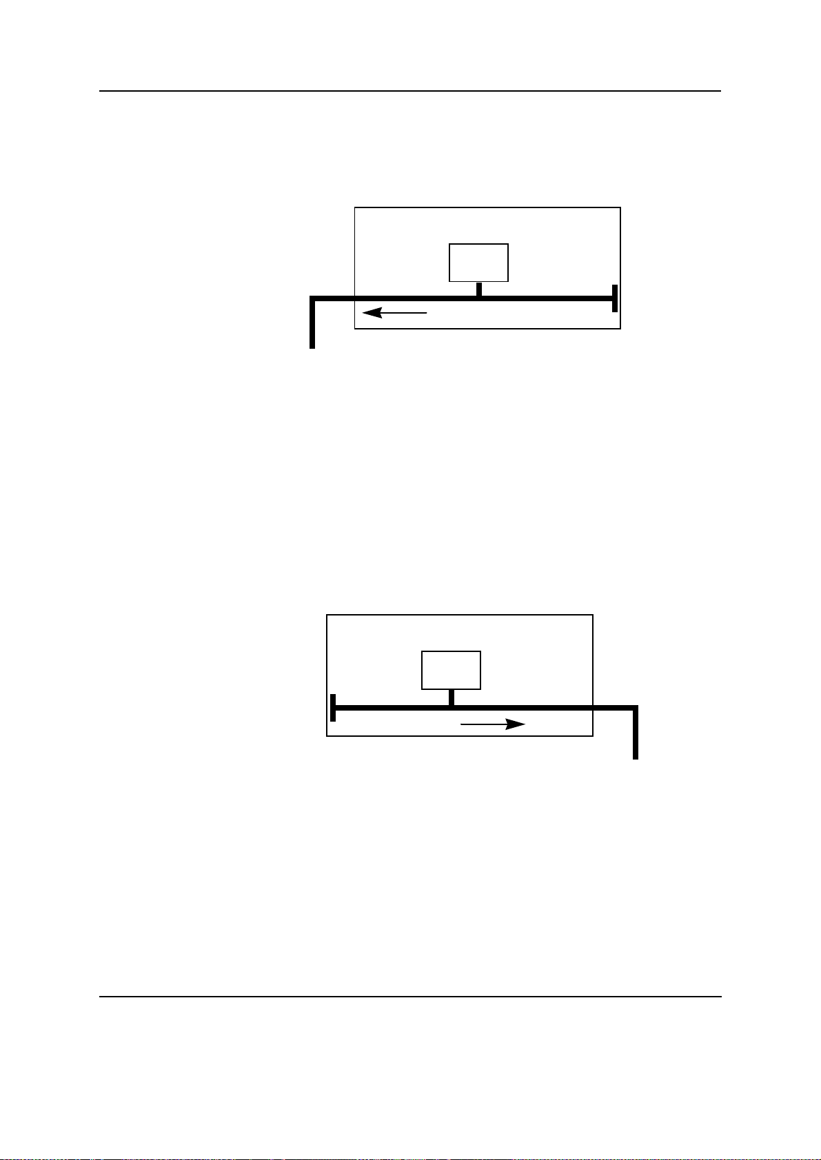
SCSI #1 Configuration Base-520(G) Installation
Alternative
configuration for
8bit SCSI
Default
configuration for
Wide SCSI
• Alternative configuration: the Base-520(G) is located at an endpoint
of the SCSI #1 bus and the CompactPCI backplane is not used for
SCSI #1 bus signalling, but the SCSI #1 bus is extended via the front
panel connector:
Front
panel
SW5-1
don’t care
SCSI cable
plugged in
Base-520(G)
SCSI #1
controller
SW5-2 = ON
CompactPCI
backplane
In this conf iguration
– both settings of SW5-1 are valid
– and SW5-2 must be set to ON = backplane termination enabled.
Wide SCSI is only available on the J5 connector of the CompactPCI
backplane.
• The Wide SCSI configuration is covered by the default switch setting: The Base-520(G) is located at an endpoint of the SCSI #1 bus,
the SCSI #1 bus is extended via the CompactPCI backplane, but no
SCSI cable is plugged into the front-panel SCSI connector:
Front
panel
SW5-1 = OFF SW5-2 = OFF
No SCSI cable
plugged in
Base-520(G)
SCSI #1
controller
Endpoint of
SCSI #1 bus
CompactPCI
backplane
The Wide SCSI termination is always enabled and it is located near
the SCSI #1 controller.
In this configuration (default switch setting):
– SW5-1 must be set to OFF = automatic enabling or disabling of
termination by sensing whether a SCSI cable is plugged in,
– and SW5-2 must be set to OFF = backplane termination disabled.
Page 40 SPARC/CPCI-52x(G)
Page 55
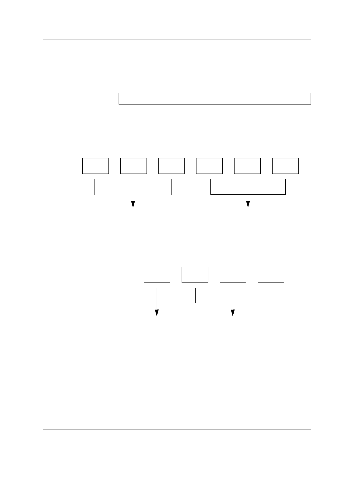
Base-520(G) Installation Ethernet Address and Host ID
4.7 Ethernet Address and Host ID
In order to see the Ethernet address and host ID, type the following command at the prompt:
ok banner
The information below explains how the SPARC/CPCI-52x(G) Ethernet
address and the host ID are determined.
Figure 14 The 48-bit (6-byte) Ethernet address
Byte543210
00 80 42
47 40 39 32 31 24 23 16 15 8 7 0
These 3 bytes always remain
0016:8016:42
16
Figure 15 The 32-bit (4-byte) host ID
Byte
These 8 bits identify
the architecture type.
3
80 YY YY
32 25 24 15 7
XXXXXX
These 3 bytes are
consecutively numbered.
2
16
These 3 bytes are
consecutively numbered.
1
8
0
Y
Y
0
SPARC/CPCI-52x(G) Page 41
Page 56

OpenBoot Firmware Base-520(G) Installation
4.8 OpenBoot Firmware
This chapte r descri bes th e use of the Ope nBoot firmwa re. Th e follow ing
tasks will be described in detail:
• Boot the system
• Run diagnostics
• Display system information
• Reset the system
• OpenBoot help
Note: The examples in this section can differ from the appearance
on your monitor according to your device tree (CPU architecture).
For more in formation on the OpenBoo t firmware see the Open Boot 3.x
Manual Set.
4.8.1 Boot the System
The OpenBoot firmware is subject to changes. For newest version and
how to upgrade refer to the SMART service accessible via the FORCE
COMPUTERS World Wide Web site.
The most important function of OpenBoot firmware is the booting of the
system. Booting is the process of loading and executing a stand-alone
program such as the operating system. After it is powered on, the system
usually boots automatically after it has passed the power-on self-test
(POST). This occurs without user intervention.
If necessary, you can explicitly initiate the boot process from the OpenBoot command interpreter. Automatic booting uses the default boot device specified in nonvolati le RAM (NVRAM); user initi ated boot ing uses
either the default boot device or one specified by the user.
To boot the system from the de fau lt boo t devi ce, ent er th e fol lowing command at the Forth monitor prompt ok:
ok boot
The boot command has the following format:
boot [
device-specifier
] [
filename
] [-
bootoption
]
Page 42 SPARC/CPCI-52x(G)
Page 57

Base-520(G) Installation OpenBoot Firmware
Optional Boot Parameters
Note: These options are specific to the operating system and may
differ fro m system to system.
[device-specifier] The name (full path or alias) of the boot devi ce. Typical values are
cdrom, disk, floppy, net, or tape.
[filename] The name of the program to be booted.
filename
is relative to th e ro o t
of the selected d evi ce. If no filename is specified, the boot c omma nd u ses
the value of
boot-file
NVRAM parameter. The NVRAM parameters
used for booting are described in the following section.
[-bootoption] Boot option may be one of the following:
[-a] -a prompt interactively for the device and name of the boot file.
[-h] -h halt after loading the program.
[-r] -r reconfigure Solari s devic e d river s after cha nging th e har dware co nfig-
uration.
[-v] -v print verbose information during boot procedure.
Devices to Boot from
To explicitly boot from the internal disk using the Forth monitor enter:
ok boot disk
To retrieve a list of all device alias definitions, type devalias
at the
Forth Monitor command prompt. The following table lists some typical
device aliases:
SPARC/CPCI-52x(G) Page 43
Page 58

OpenBoot Firmware Base-520(G) Installation
Page 44 SPARC/CPCI-52x(G)
Page 59

Base-520(G) Installation OpenBoot Firmware
Table 20 Device alias definitions
Alias Description
Defined for SCSI
scsi
disk
disk6
disk5
disk4
disk3
disk2
disk1
disk0
tape (or tape0)
tape1
cdrom
net
SCSI
Default disk SCSI-target-ID 0
disk SCSI-target-ID 6
disk SCSI-target-ID 5
disk SCSI-target-ID 4
disk SCSI-target-ID 3
disk SCSI-target-ID 2
disk SCSI-target-ID 1
disk SCSI-target-ID 0
1st tape drive SCSI-target-ID 4
2nd tape drive SCSI-target-ID 5
CD-ROM partition f, SCSI-target-ID 6
Defined for Ethernet
Ethernet
floppy
audio
keyboard
mouse
ebus
pcia
pcib
pci
flash-prog
flash
ttya
ttyb
Floppy disk
Audio
Keyboard
Mouse
EBus2
secondary PCI bus A
secondary PCI bus B
primary PCI bus
Flash EPROM programming mode
Flash EPROM
Serial interface A
Serial interface B
SPARC/CPCI-52x(G) Page 45
Page 60

OpenBoot Firmware Base-520(G) Installation
4.8.2 NVRAM Boot Parameters
The OpenBoot firmware holds its configuration parameters in NVRAM.
At the Forth monitor pr ompt en ter print env to see a list of all available
configuration parameter s.
Note: Per default the SPARC/CPCI-52x(G) boots the OS
automatically. If not, ensure that the auto-boot? parameter is
always set to true.
To set
parameters
The OpenBoot command setenv may be u sed to se t spe cifi c para mete rs
in the order below:
setenv [
configuration_parameter
The configuration parameters in Table 2 are involved with the boot process.
Table 21 Setting configuration parameters
Parameter Default value Description
auto-boot? true
boot-device disk
boot-file empty string
diag-switch? false
diag-device net
diag-file empty string
If true, automatic booting after power on or reset
Device from which to boot
File to boot
If true, run in diagnostic mode
Device from which to boot in diagnostic mode
File to boot in diagnostic mode
When booting an operating system or another stand-alone program, and
neither a boot device nor a filename is supplied, the boot command of
the Forth monitor takes the omitted values from the NVRAM configuration parameters. If the parameter diag-switch? is false,
boot-device and boot-file are used. Otherwise, the OpenBoot
firmware uses diag-device and diag-file for booting.
] [
value
]
4.8.3 Diagnostics
At Hardware Power On or Button Power On the Ope nBoot f ir mwa re e xecutes POST. The extent of c ert ai n t es ts exe cut ed within the POST depend
on the state of the configuration parameter diag-level. The operator
can choose between minimal or maximal testing by setting this configuration parameter to min or max. Furthermore an enhanced diagnostic
menu is av ailab le i f setti ng this p ara mete r to menu. If the NVRAM con-
Page 46 SPARC/CPCI-52x(G)
Page 61

Base-520(G) Installation OpenBoot Firmware
figuration parameter diag-switch? is true for each test, a message
is displayed on a terminal connected to the serial I/O interface A. If the
system does not work correctly, error messages are displayed which indicate the problem. After POST the OpenBoot firmware boots an operating
system or enters the Forth moni tor, if the NVRAM configu ratio n parameter auto-boot? is false.
The Forth Monitor includes several diagnostic routines. These on-board
tests let you check devices such as network controller, SCSI devices,
floppy disk sys tem, cl ock , k eybo ar d and audio. User i nst al led devices can
be tested if their firmware includes a self-test routine.
The table below lists several diagnostic routines followed by examples
for each of these routines:
Table 22 Diagnostic routines
Command Description
probe-scsi
probe-scsi-all [
test
device-specifier
test-all [
watch-clock
watch-net-all
watch-net
device-specifier
device-path
Identifies devices connected to the primary SCSI bus
]
Performs probe-SCSI on all SCSI buses installed in
the system below the specified device tree node. If
device-path
is omitted, the root node is used.
Executes the specified device’s self-test method.
device-specifier
may be a device path name
or a device alias.
Example:
• test net – test network connection
]
Tests all devices that have a built-in self-test method
and that reside below the specified device tree node.
device-path
If
is omitted , the root node is used.
Monitors the clock function.
Monitors network connection via all Ethernet inter-
faces installed in the system.
Monitors network connection via primary Ethernet.
Examples:
SCSI bus To check the SCSI #1 for connected devices enter:
ok probe-scsi
Target 3
Unit 0 Disk FUJITSU M2952ESP SUN2.1G2545
ok
SPARC/CPCI-52x(G) Page 47
Page 62

OpenBoot Firmware Base-520(G) Installation
All SCSI buses To check all the SCSI buses installed in the system enter the following
(The actual response depends on the devices on the SCSI buses).:
ok probe-scsi-all
/pci@1f,0/scsi@2
Target 6
Unit 0 Disk Removable Read Only Device SONY CD-ROM CDU-8012 3.1a
/pci@1f/pci@4,1/scsi@2
Target 3
Unit 0 Disk FUJITSU M2952ESP SUN2.1G2545
ok
Note: The command probe-scsi-all can last up to 2 minutes
without terminal message.
Single device To test a single installed device enter:
ok test
device-specifier
This executes the self-test device method of the specified device
node.
device-specifier
may be a device path name or a device alias as
described in Table 20, “Device alias definitions,” on page 45. The re-
sponse depends on the self-test of the device node.
Group of devices To test a group of installed devices enter:
ok test-all
All devices below the root node of the device tree are tested. The response depends on the de vic es having a self-test rou ti ne. If a device specifier option is supplied at the command line, all devices below the
specified device tree node are test ed.
Clock To test the clock function enter:
ok watch-clock
Watching the ‘seconds’ register of the real time clock
chip.
It should be ‘ticking’ once a second.
Type any key to stop.
22
ok
Page 48 SPARC/CPCI-52x(G)
Page 63

Base-520(G) Installation OpenBoot Firmware
The system responds by incrementing a number once a second. Press any
key to stop the test.
Network To monitor the network connection enter:
ok watch-net
Internal loopback test -- succeeded.
Transceiver check -- Using Onboard transceiver -- Link Up.
passed
Using Onboard transceiver -- Link Up.
Looking for Ethernet packets.
‘.’ is a good packet. ‘X’ is a bad packet.
Type any key to stop.
...........X...........................X..............
ok
The system monitors the network traffic, displaying a dot (.) each time
it receives a val id pack et and dis playin g an X each time i t rec eives a packet with an error which can be detected by the network hardware interface.
4.8.4 Display System Information
The Forth monitor provides several commands to display system information. These commands let you display the system banner, the Ethernet
address for the Ethernet controller, the contents of the ID PROM, and the
version number of the OpenBoot firmware.
The ID PROM contains speci fic information to the individual m achine,
including the serial number, date of manufacture, and assigned Ethernet
address.
The following table lists these commands:
Table 23 Commands to display system information
Command Description
banner
show-pci-devs-all
.enet-addr
.idprom
.traps
Displays system banner
Displays list of installed and probed PCI Bus
devices
Displays the Ethernet address
Displays ID PROM contents, formatted
Displays a list of SPARC trap types
.version
show-devs
devalias
SPARC/CPCI-52x(G) Page 49
Displays version and date of the boot PROM
Displays a list of all device tree nodes
Displays a list of all device aliases
Page 64

OpenBoot Firmware Base-520(G) Installation
4.8.5 Reset the System
If your system needs to be reset, you either press the reset button on the
front panel or, if you are i n the F orth Moni to r, type reset on the command
line.
ok reset
The system immediately begins executing the initialization procedures
and executes the POST if having pressed the reset button. Then the system either boots automatically or enters the Forth Monitor, just as it
would have done after a power-on cycle.
4.8.6 OpenBoot Help
The Forth Monitor contains an online help which can be activated by entering:
ok help
Enter ‘help command-name’ or ‘help category-name’ for more help
(Use ONLY the first word of a category description)
Examples: help select -or- help line
Main categories are:
Numeric output
Radix (number base conversions)
Arithmetic
Memory access
Line editor
System and boot configuration parameters
Select I/O devices
Floppy eject
Power on reset
Diag (diagnostic routines)
Resume execution
File download and boot
Nvramrc (making new commands permanent)
ok
A list of all available help categories is displayed. These categories may
also contain subcategories. To get help for special Forth words or subcategories just type help [name].
• The online help sho ws you the For th wor d, the p aramete r sta ck bef ore
and after execution of the Forth word (before -- after), and a short
description.
• The onlin e help of the Fort h monitor is locat ed in the boot PR OM,
that means that there is not an online help for all Forth words.
Page 50 SPARC/CPCI-52x(G)
Page 65

Base-520(G) Installation OpenBoot Firmware
Example:
How to get help for special Forth words or subcategories:
ok help power
reset-all reset-machine, (simulates power cycling )
power-off Power Off
ok
ok help memory
dump ( addr length -- ) display memory at addr for length bytes
fill ( addr length byte -- ) fill memory starting at addr with byte
move ( src dest length -- ) copy length bytes from src to dest address
map? ( vaddr -- ) show memory map information for the virtual address
x? ( addr -- ) display the 64-bit number from location addr
l? ( addr -- ) display the 32-bit number from location addr
w? ( addr -- ) display the 16-bit number from location addr
c? ( addr -- ) display the 8-bit number from location addr
x@ ( addr -- n ) place on the stack the 64-bit data at location addr
l@ ( addr -- n ) place on the stack the 32-bit data at location addr
w@ ( addr -- n ) place on the stack the 16-bit data at location addr
c@ ( addr -- n ) place on the stack the 8-bit data at location addr
x! ( n addr -- ) store the 64-bit value n at location addr
l! ( n addr -- ) store the 32-bit value n at location addr
w! ( n addr -- ) store the 16-bit value n at location addr
c! ( n addr -- ) store the 8-bit value n at location addr
ok
SPARC/CPCI-52x(G) Page 51
Page 66

OpenBoot Firmware Base-520(G) Installation
Page 52 SPARC/CPCI-52x(G)
Page 67

I/O-52x(G) Installation Location Overview
5 I/O-52x(G) Installation
5.1 Location Ov erview
The I/O-52x(G) contains the following main I/O interfaces:
• SCSI #2,
• Ethernet #2,
• PMC #1 and PMC #2.
SPARC/CPCI-52x(G) Page 53
Page 68
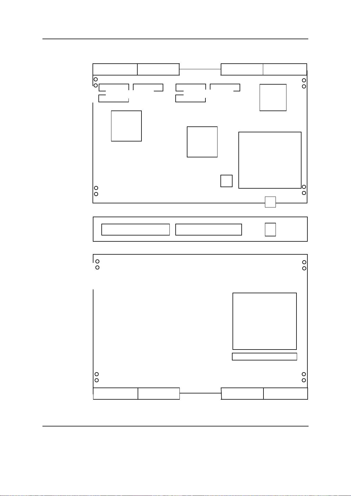
Location Overview I/O-52x(G) Installation
Figure 16 Location diagram of the I/O-52x(G) (schematic)
J1J5 J2J4
PN 22 PN 24
PMC #2 connectors
PN 21
Top
SCSI #2
Front panel (1 slot high)
PMC #2
PN 12 PN 14
PMC #1 connectors
PN 11
Ethernet #2
PHYceiver
PMC #1
APB
CPU and cache
heatsink
ETHERNET
Bottom
CPU and cache
heatsink
Base-520(G) connector P6
J1J5 J2J4
Page 54 SPARC/CPCI-52x(G)
Page 69
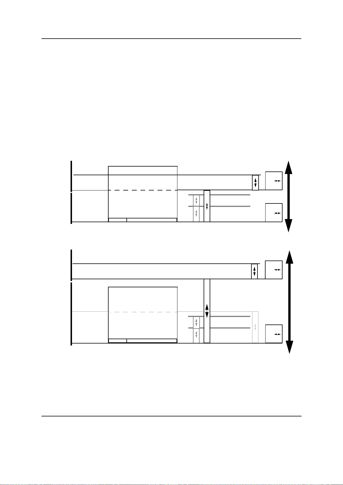
I/O-52x(G) Installation Mechanical Constructions
5.2 Mechanical Constructions
The I/O-52x(G) is an extension to the Base-520(G). It occupies
1 CompactPCI slot and consists of the following major components:
• 2 PMC connectors,
• 1 SCSI #2 interface,
• and 1 Ethernet #2 interface.
The following figures show the SPARC/CPCI-52x(G) i n 2-slot and 3-slot
configurations.
Figure 17 Mechanical construction of the SPARC/CPCI-522
F
r
o
2 PMC modules
n
I/O-522
t
in the 2nd slot
P
a
n
e
l
Base-520 in
s
1st slot
CPU and cache with
heatsink
MEM-50U
MEM-50L
B
a
c
k
p
l
a
n
e
Figure 18 Mechanical construction of the SPARC/CPCI-52xG
2 PMC modules
F
r
I/O-52xG
o
in the 3rd slot
n
t
P
a
n
UPA64S card
e
l
s
Base-520G
in 1st slot
CPU and cache with
heatsink
MEM-50U
MEM-50L
B
a
c
k
p
l
a
n
e
SPARC/CPCI-52x(G) Page 55
Page 70
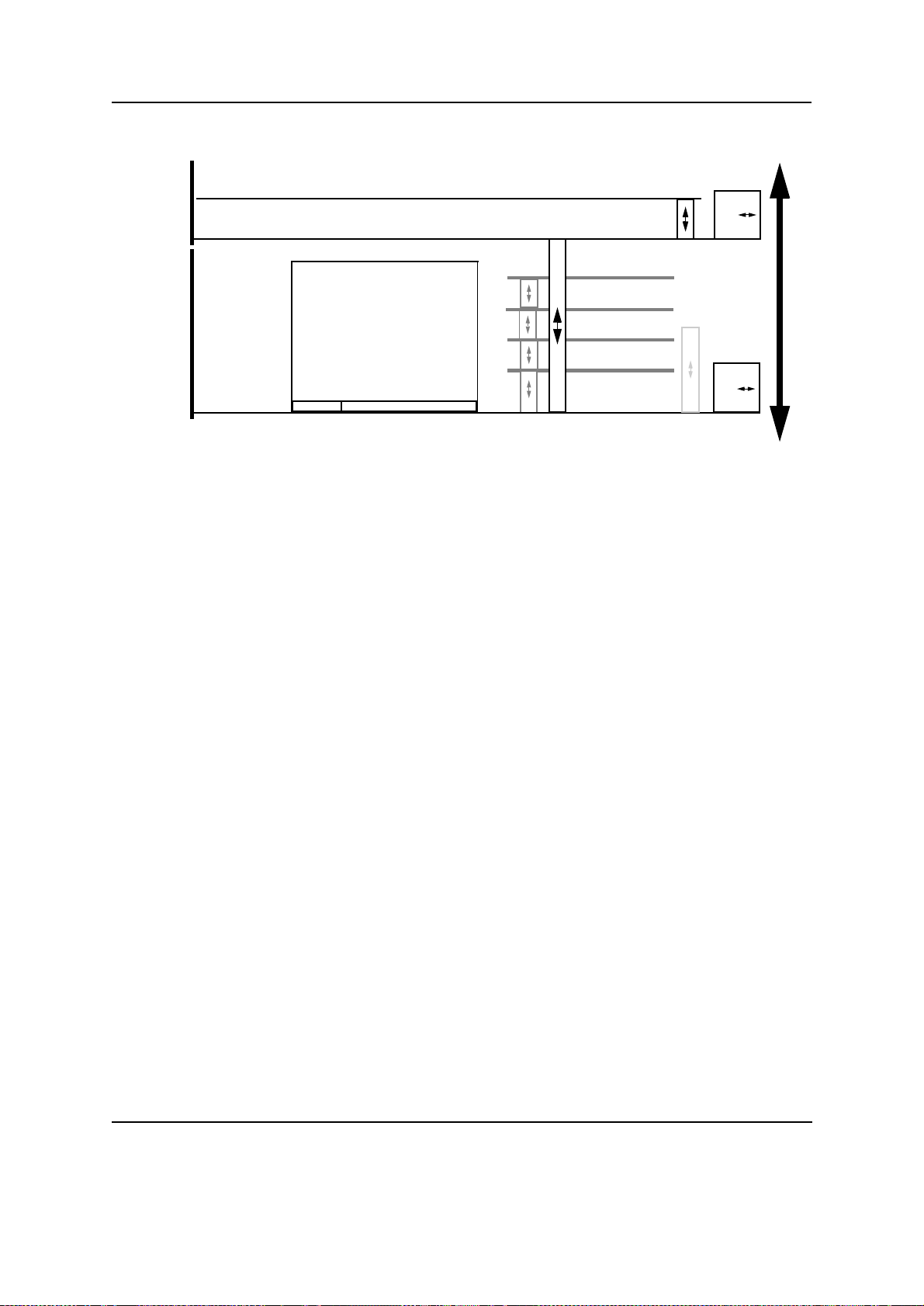
Mechanical Constructions I/O-52x(G) Installation
Figure 19 Mechanical construction of the SPARC/CPCI-52xG (option)
2 PMC modules
F
r
I/O-52xG
o
in the 3rd slot
n
t
P
a
n
e
l
s
Base-520G
in 1st slot
CPU and cache with
heatsink
MEM-50U
MEM-50M
MEM-50M
MEM-50L
B
a
c
k
p
l
a
n
e
5.2.1 Installation/Deinstallation of the I/O-52x(G)
This section desc ri bes the installation and deinstallation procedure f or the
I/O-52x(G) with the mentioned location shown in the figure below.
Installation of
the I/O-52x(G)
Deinstallation of
the I/O-52x(G)
To install the I/O-52x(G) follow the steps below:
1. If there is an UPA64S card installed on your Base-520(G) ensure that
you use the 2 z-standoffs delivered with the UPA64S card.
2. Remove the 10 screws at location 1...6 on the open end off the standoffs of the I/O-52x(G).
3. Plug the I/O-52x(G) to the Base-520(G) via the I/O-52x(G) to
Base-520(G) connector at position 7 and fix it with the 10 removed
screws on the standoffs at location 1...6.
To deinstall the I/O-52x(G) follow the steps below:
1. Remove the 8 screws at location 1...4 on the bottom side of your
Base-520(G).
2. Remove the 2 screws at location 5 and 6 on the top side of the
I/O-52x(G).
3. Remove the I/O-52x(G) from the Base-520(G) by lifting it.
4. Fix the removed 10 screws on the open ends of the standoffs to have
them available when installing the I/O-52x(G) again.
Page 56 SPARC/CPCI-52x(G)
Page 71
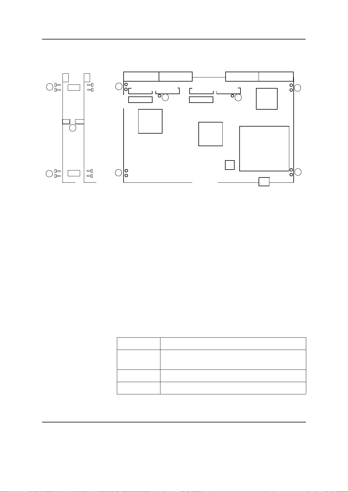
I/O-52x(G) Installation Powering Up
Figure 20 Installation/Deinstallation of the I/O-52x(G)
Base520(G)
I/O-52x(G)
I/O-52x(G)
J1J5 J2J4
1
Standoff
7
2
Side view Top view
5.3 Powering Up
1
PMC#2 connectors
6
PMC#1 conne ctors
4
5
APB
Top
SCSI
Ethernet
CPU and cach e
heatsink
2
Front panel
PHYceiver
3
For powering up see the respective installation section of the
Base-520(G).
5.4 Front Panel and Connectors
Front panel
features
Table 24 Front panel features
SPARC/CPCI-52x(G) Page 57
The features of the front panel are described in the following table. For a
location diagram see figure 14 “Location diagram of the I/O-board (schematic)” on page 47.
Device Description
ETHERNET Standard Twisted-Pair-Ethernet RJ45 connector for
10BaseT/100BaseTX Ethernet
PMC #1 Hole for the PMC #1 front panel
PMC#2 Hole for the PMC #2 front panel
Page 72
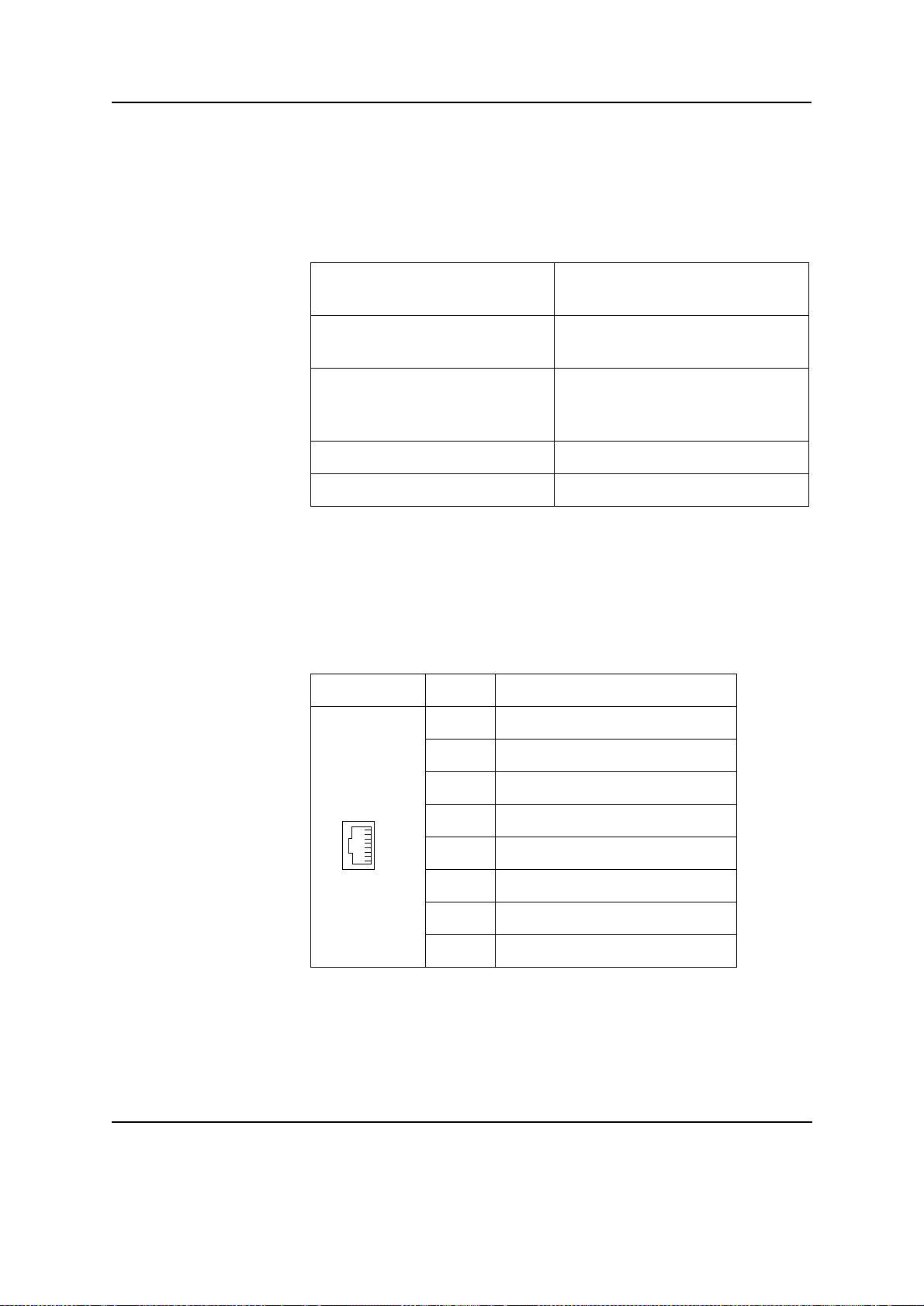
Front Panel and Connectors I/O-52x(G) Installation
On-board
connectors
In addition to the front-panel connectors, the I/O-52x(G) provides onboard connectors for connection to the Base-520(G), to the CompactPCI
bus and for 2 PMC modules. An overview is shown in the following table.
Table 25 On-board connectors
Connector description and
location
CompactPCI J1, J2, J4, J5 Standard CompactPCI metric,
I/O-52x(G) extension connectorP6100-pin MBUS connector female
PMC #1 PN11, PN12, PN14 64-pin SMD connector
PMC #2 PN21, PN22, PN24 64-pin SMD connector
5.4.1 Ethernet #2 Interfaces
Connector type and sample
manufacturer part number
5-row shielded connectors female
low: for 2 s l ot solution
high: for 3 slot solution
The full duplex 10BaseT/100BaseTx Ethernet #2 interface is available at
the front panel via a Twisted-Pair-Ethernet connector.
Table 26 Twisted-Pair-Ethernet connector pinout
Connector Pin Signal
1TX+
2TX-
RJ-45 TPE
1
8
3RX+
4GND
5GND
6RX-
7GND
8GND
The Ethernet #2 interface i s als o ac cessi ble at the J5 back pan el conn ector
via an MII #2 interface.
If Ethernet #2 gets accessed via I/O panel, the
front panel connector is normally disabled automatically, for other configurations see the respective jumper settings in the SPARC/IOBP-520
Page 58 SPARC/CPCI-52x(G)
Page 73

I/O-52x(G) Installati on Front Panel and Connectors
Installation Guide. For the J5 connector pinout see fi gur e 22 “CompactP-
CI J5 connector pinout” on page 60.
5.4.2 PMC Slots
The I/O-52x(G) provides 2 PMC slots compliant with IEEE P1386
("Draft Standard Physical and Environmental Layers for PCI Mezzanine
Cards: PMC"). The PCI bus, a high speed local bus, connects different
high speed I/O cards with the SPARC/CPCI-52x(G). Both PMC slots
support 32-bit data bus width with a maximum frequency of 33 MHz.
PMC Voltage
Keys
Connector
Configuration
The PCI bus uses a 5V voltage to signal bus levels. The voltage keys prevent 3.3V PMC cards from being plugged into the PMC slots.
The 32-bit PCI bus requires 2 PMC connectors. The 3rd PMC connector
(PNx4) connects additional user I/O signals of PMC slot 1 and PMC
slot 2 to the CompactPCI J4 connector.
PMC slot 1
connectors
PMC slot 2
connectors
• for the PCI bus: PN11 and PN12
• for 64 user I/O signals: PN14
• for the PCI bus: PN21 and PN22
• for 32 user I/O signals: PN24
5.4.3 CompactPCI Backplane Connector Pinout
J1 and J2 The J1 and J2 connectors implement the CompactPCI 64-bit connector
pinout as specified by the CompactPCI specification. Therefore, this
manual only documents the pinout of the J4 and J5 connector.
J4 and J5 Besides the CompactPCI specific pinout the following interfaces are
available on the CompactPCI J4 and J5 connector.
• SCSI #2, MII #2
• User I/O pins for PMC #1 and #2 (PMC #1, PMC #2)
SPARC/CPCI-52x(G) Page 59
Page 74
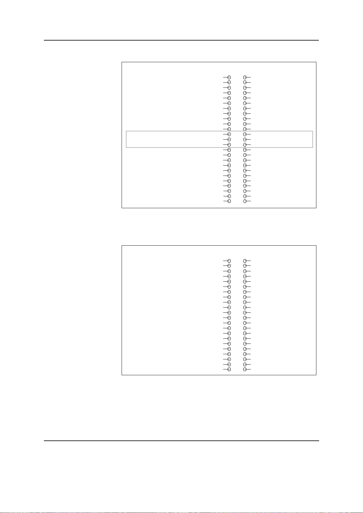
Front Panel and Connectors I/O-52x(G) Installation
Figure 21 CompactPCI J4 connector pinout
BA
PMC #1 I/O 61
PMC #1 I/O 56
PMC #1 I/O 51
PMC #1 I/O 46
PMC #1 I/O 41
PMC #1 I/O 36
PMC #1 I/O 31
PMC #1 I/O 26
PMC #1 I/O 21
PMC #1 I/O 16
PMC #1 I/O 11
PMC #1 I/O 62
PMC #1 I/O 57
PMC #1 I/O 52
PMC #1 I/O 47
PMC #1 I/O 42
PMC #1 I/O 37
PMC #1 I/O 32
PMC #1 I/O 27
PMC #1 I/O 22
PMC #1 I/O 17
PMC #1 I/O 12
PMC #1 I/O 63
PMC #1 I/O 58
PMC #1 I/O 53
PMC #1 I/O 48
PMC #1 I/O 43
PMC #1 I/O 38
PMC #1 I/O 33
PMC #1 I/O 28
PMC #1 I/O 23
PMC #1 I/O 18
PMC #1 I/O 13
Coding key area
PMC #1 I/O 6
PMC #1 I/O 1
PMC #2 I/O 61
PMC #2 I/O 56
PMC #2 I/O 51
PMC #2 I/O 46
PMC #2 I/O 41
PMC #2 I/O 36
PMC #2 I/O 31
PMC #2 I/O 26
PMC #2 I/O 21
PMC #1 I/O 7
PMC #1 I/O 2
PMC #2 I/O 62
PMC #2 I/O 57
PMC #2 I/O 52
PMC #2 I/O 47
PMC #2 I/O 42
PMC #2 I/O 37
PMC #2 I/O 32
PMC #2 I/O 27
PMC #2 I/O 22
PMC #1 I/O 8
PMC #1 I/O 3
PMC #2 I/O 63
PMC #2 I/O 58
PMC #2 I/O 53
PMC #2 I/O 48
PMC #2 I/O 43
PMC #2 I/O 38
PMC #2 I/O 33
PMC #2 I/O 28
PMC #2 I/O 23
As factory option the PMC #1 I/O 1...32 signals can be connected to the
PMC #2 I/O 33...64 signals.
Figure 22 CompactPCI J5 connector pinout
DC
1
2
3
4
5
6
7
8
9
10
11
12
13
14
15
16
17
18
19
20
21
22
23
24
25
PMC #1 I/O 64
PMC #1 I/O 59
PMC #1 I/O 54
PMC #1 I/O 49
PMC #1 I/O 44
PMC #1 I/O 39
PMC #1 I/O 34
PMC #1 I/O 29
PMC #1 I/O 24
PMC #1 I/O 19
PMC #1 I/O 14
PMC #1 I/O 9
PMC #1 I/O 4
PMC #2 I/O 64
PMC #2 I/O 59
PMC #2 I/O 54
PMC #2 I/O 49
PMC #2 I/O 44
PMC #2 I/O 39
PMC #2 I/O 34
PMC #2 I/O 29
PMC #2 I/O 24
E
n.c.
PMC #1 I/O 60
PMC #1 I/O 55
PMC #1 I/O 50
PMC #1 I/O 45
PMC #1 I/O 40
PMC #1 I/O 35
PMC #1 I/O 30
PMC #1 I/O 25
PMC #1 I/O 20
PMC #1 I/O 15
PMC #1 I/O 10
PMC #1 I/O 5
VP5_IOBP
PMC #2 I/O 60
PMC #2 I/O 55
PMC #2 I/O 50
PMC #2 I/O 45
PMC #2 I/O 40
PMC #2 I/O 35
PMC #2 I/O 30
PMC #2 I/O 25
SCSI #2 D8
SCSI #2 SEL
SCSI #2 ATN
SCSI #2 D4
SCSI #2 D0
SCSI #2 D12
MII #2 RXD3
MII #2 RX_DV
MII #2 TXD3
PMC #2 I/O 19
PMC #2 I/O 14
PMC #2 I/O 9
PMC #2 I/O 5
PMC #2 I/O 1
VP5_IOBP
n.c.
n.c.
n.c.
n.c.
n.c.
n.c.
n.c.
SCSI #2 D9
SCSI #2 CD
SCSI #2 BSY
SCSI #2 D5
SCSI #2 D1
SCSI #2 D13
MII #2 RXD2
MII #2 COL
MII #2 TXD2
PMC #2 I/O 20
PMC #2 I/O 15
PMC #2 I/O 10
PMC #2 I/O 6
PMC #2 I/O 2
n.c.
n.c.
n.c.
n.c.
n.c.
n.c.
n.c.
n.c.
BA
SCSI #2 D10
SCSI #2 REQ
SCSI #2 ACK
SCSI #2 D6
SCSI #2 D2
SCSI #2 D14
MII #2 RXD1
MII #2 CRS
MII #2 TXD1
MII #2 TX_EN
PMC #2 I/O 16
PMC #2 I/O 11
PMC #2 I/O 7
PMC #2 I/O 3
n.c.
n.c.
n.c.
n.c.
n.c.
n.c.
n.c.
n.c.
DC
1
2
3
4
5
6
7
8
9
10
11
12
13
14
15
16
17
18
19
20
21
22
SCSI #2 D11
SCSI #2 IO
SCSI #2 RST
SCSI #2 D7
SCSI #2 D3
SCSI #2 D15
MII #2 RXD0
MII #2 RX_ER
MII #2 TXD0
MII #2 TX_ER
PMC #2 I/O 17
PMC #2 I/O 12
PMC #2 I/O 8
PMC #2 I/O 4
n.c.
n.c.
n.c.
n.c.
n.c.
n.c.
n.c.
n.c.
E
n.c.
WIDETERMPWR
SCSI #2 MSG
TERMPWR
SCSI #2 DP0
SCSI #2 DP1
MII #2 RX_CLK
MII #2 MGT_DIO
MII #2 TX_CLK
MII #2 MGT_CLK
PMC #2 I/O 18
PMC #2 I/O 13
VP5_IOBP
n.c.
n.c.
n.c.
n.c.
n.c.
n.c.
n.c.
n.c.
n.c.
I/O panel As a separate price list item an I/O panel is available for the I/O-52x(G),
the SPARC/IOBP-520/IO. An extended variant is the SPARC/CPCI520/AccKit/IO which contai ns additionally to the I/O panel the following
cables:
– a flat ribbon SCSI cable for the I/O panel
Page 60 SPARC/CPCI-52x(G)
Page 75

I/O-52x(G) Installati on Front Panel and Connectors
– and a Twisted-Pair-Ethernet cable for the front panel or the I/O
panel.
The I/O panel supports the following interfaces:
• Fast/Wide SCSI #2,
• MII #2 Ethernet,
•and PMC user I/O.
Danger The SPARC/IOBP-520/IO and the SPARC/CPCI-520/AccKit/IO is
especially designed for the I/O-52x(G).
Do not use any other I/O panel s on the I/O-52x(G). Use only the fr ont
panel or the backpanel Ethernet interface, not both. Check the configuration of your I/O panel.
SPARC/CPCI-52x(G) Page 61
Page 76
SCSI #2 Configuration I/O-52x(G) Installation
5.5 SCSI #2 Configuration
Note: Correct SCSI bus selection: The I/O-52x(G) provides a
second SCSI bus, SCSI #2. Its configuration is described as follows.
The I/O-52x(G)’s SCSI #2 bus is only available at the I/O-52x(G)’s
CompactPCI J5 connector.
Valid
configuration
There is only 1 valid I/O-52x(G) SCSI #2 bus configuration:
• The I/O-52x(G) is located at an endpoint of the SCSI #2 bus, the
SCSI #2 bus is extended via the CompactPCI backplane:
Front
panel
The SCSI #2 bus is always terminated at the SCSI #2 controller.
5.6 Ethernet #2 Configuration
Note: Correct Ethernet selection: The I/O-52x(G) provides the
following 2 Ethernet #2 interfaces:
I/O-52x(G)
SCSI #2
controller
CompactPCI
backplane
Endpoint of
SCSI #2 bus
• via a TPE #2 interface connected to a front-panel RJ-45 connector
• or an MII #2 interface available at the CompactPCI J5 connector
Ethernet address
and host ID
For the SPARC/CPCI-52x(G) exists only 1 ethernet address and host ID,
see "Ethernet Address and Host ID" section of the Base-520(G)’s installation section. Therefore you can use the Ethernet #2 TPE or MII interface of the I/O-52x(G) only in a separate network according to
Ethernet #1 TPE or MII of the Base-520(G).
Page 62 SPARC/CPCI-52x(G)
Page 77

I/O-52x(G) Installation OpenBoot Firmware Alias Definitions for I/O-52x(G)
5.7 OpenBoot Firmware Alias Defi nitions for I/O-52x(G)
This chapter describes additional features used with reference to the
I/O-52x(G) enhancements.
Table 27 Device alias definitions
Alias Description
Defined fo r SCSI #2:
scsi-2
disk26
disk25
disk24
disk23
disk22
disk21
disk20
tape2 (or tape20)
tape21
cdrom2
net
pcia-io
SCSI #2
disk SCSI #2-target-ID 6
disk SCSI #2-target-ID 5
disk SCSI #2-target-ID 4
disk SCSI #2-target-ID 3
disk SCSI #2-target-ID 2
disk SCSI #2-target-ID 1
disk SCSI #2-target-ID 0
1st tape drive SCSI #2-target-ID 4
2nd tape drive SCSI #2-target-ID 5
CD-ROM partition f, SCS I #2-target-ID 6
Defined for Ethernet #2:
Ethernet #2
secondary PCI bus A
pcib-io
SPARC/CPCI-52x(G) Page 63
secondary PCI bus B
Page 78

OpenBoot Firmware Alias Definitions for I/O-52x (G) I/O- 52x(G) Installati on
Page 64 SPARC/CPCI-52x(G)
Page 79

Hardware Description
6 Hardware Description
The SPARC/CPCI-52x(G) is a high performance CompactPCI board
computer providing a CompactPCI system controller interface including
DMA. It is based on
• the UltraSPARC-IIi processor supporting 3 high-speed interfaces
concurrently operating:
– the memory interface with ECC
– the external (L2) cache interface
– the 66 MHz PCI interface.
• and the APB (A dv an ce d PCI Brid g e) w it h i nte rf ac es to th e Co mp a ct PCI bus
The base board carries the components of the UltraSPARC-IIi chip set:
• the XCVR data multiplexers,
• the UIC (UPA Interrupt Concentrator) and
Described
features of the
Base-520(G)
Described
features of the
I/O-52x(G)
• the PCIO (PCI IO) chip which interfaces to the local I/O bus.
The Base-520G is fully functional without the I/O-52x(G). Besides the
CompactPCI interface the SPARC/CPCI-52x(G) provides the following
components on the 2 on-board buses – the PCI bus and the EBus2:
• Ethernet interface (Twisted-Pair and MII) Ethernet #1
• Ultra-wid e SCSI interface SCSI # 1
• Boot PROM, boot flash EPROM, and user flash EPROM
• 2 Serial Interfaces – SAB 82532
• Keyboard/Mouse, FDC and Parallel Interface – Super I/O
• RTC/NVRAM – M48T58
• 16-bit stereo audio interface
• System configuration regi st er s
• 7- segments LED, rotary-switch, sy stem and user LEDs
The I/O-52x(G) adds
• 2 PMC Slots with Busmode Support,
• the second SCSI interface SCSI #2,
• and a second Ethernet interface Ethernet #2.
SPARC/CPCI-52x(G) Page 65
Page 80
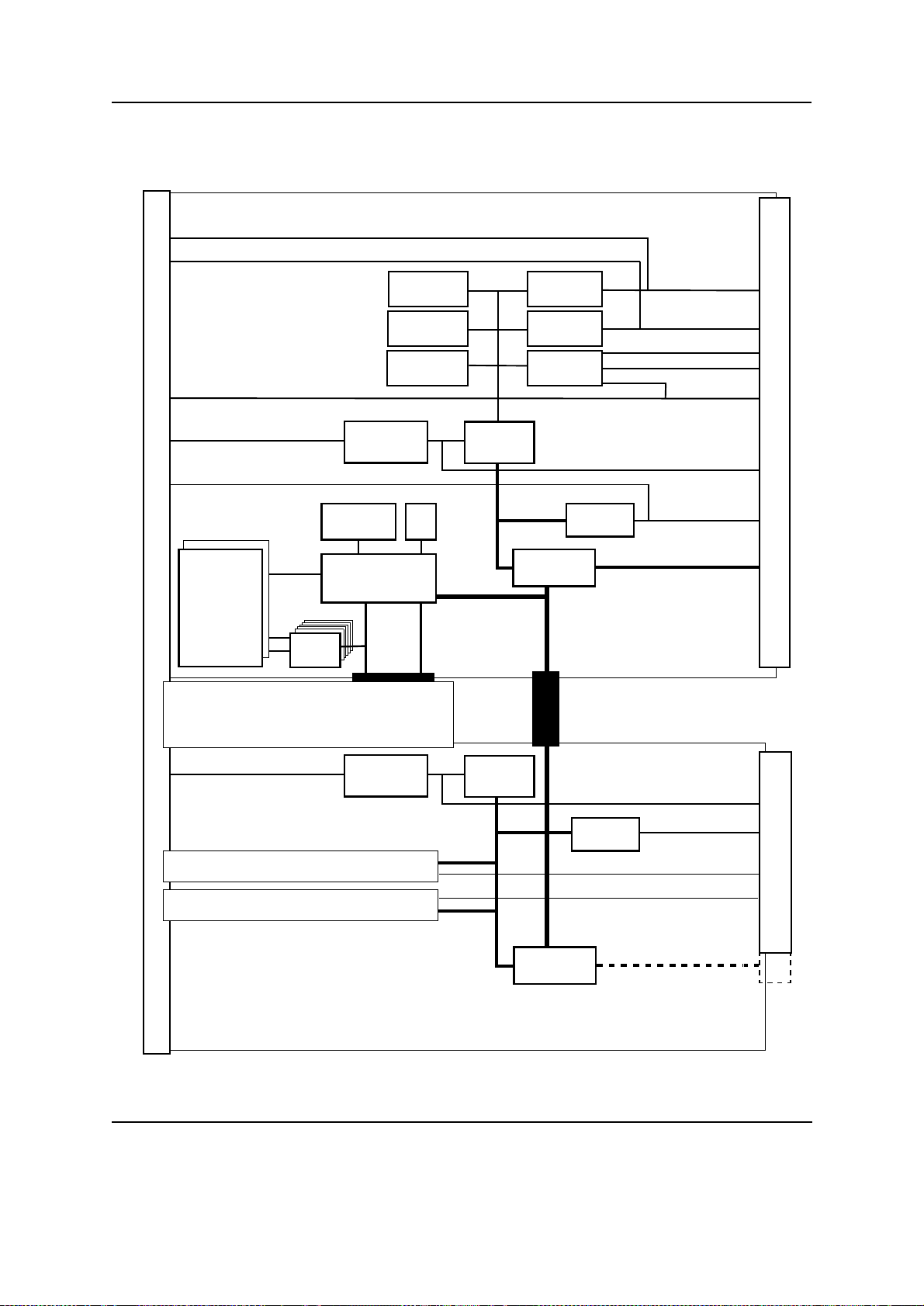
Figure 23 Block Diagram of the SPARC/CPCI-52x(G)
Dual serial
Audio (hdph, micro)
Hardware Description
Base board
Keyboard/mouse
10/100Base-Tx Ethernet #1
SCSI #1
F
r
o
n
t
p
a
n
e
l
s
Memory
modules
Addr.
and ctrl.
UPA64S card
L2 Cache
XCVR
User flash
Boot flash
NVRAM
Ethernet #1
PHYceiver
UIC
UltraSPARC-IIi
Memory
data
RTC
PCI bus B
Addr. and
ctrl
EBus2
PCIO
Ethernet #1
PCI-to-dualPCI bridge
Serial I/O
Audio
Super-I/O
SCSI #1
PCI bus
Board-to-board
high-speed
connector
Dual serial
Audio (hdph,micro)
Parallel
Floppy
Keyboard/mouse
MII Ethernet #1
SCSI #1
PCI bus A
I/O board
C
o
m
p
a
c
t
P
C
I
10/100Base-Tx Ethern et #2
PMC slot #2 with 5V I/O
PMC slot #1 with 5V I/O
Ethernet #2
PHYceiver
PCIO
Ethernet #2
PCI bus B
PCI-to-dualPCI bridge
SCSI #2
only in case of I/O 523 G
MII Ethernet #2
SCSI #2
PMC #2 I/O
PMC #1 I/O
PCI bus A
C
o
m
p
a
c
t
P
C
I
Page 66 SPARC/CPCI-52x(G)
Page 81

Hardware Description
Table 28 Buses, bus modes, and connected devices
Bus and
bus mode Connected Devices
The following table gives an overview of the different buses, their bus
modes, and the connected devices.
EC bus,
big endian
Memory bus,
big endian
UPA bus,
big endian
PCI bus,
little endian
PCI A bus on
Base-520(G),
little endian
PCI bus B on
Base-520(G),
little endian
EBus2,
little endian
• UltraSPARC-IIi (see page 68)
• L2 cache with tag (see page 70)
• UltraSPARC-IIi (see page 68)
• Memory banks (see page 70)
• UltraSPARC-IIi (see page 68)
• UPA64S card
• UltraSPARC-IIi (see page 68)
• APB on Base-520(G) and on I/O-52x(G) (see page 75)
• APB (see page 75)
• CompactPCI interface (see page 75)
• APB (see page 75)
• Ethernet controller with EBus2 interface (PCIO) (see page 75)
• SCSI controller (see page 97)
• Serial I/ O interfaces ( see page 80)
• Keyboard/Mouse, parallel and floppy interface (see page 81)
• Audio interface (see page 84)
• RTC/NVRAM (see page 83)
• Boot PROM, boot and user flash EPROM (see page 79)
• System Configuration Registers (see page 85)
PCI bus A on
I/O-52x(G),
little endian
PCI bus B on
I/O-52x(G),
little endian
• APB (see page 75)
• only I/O-523G: CompactPCI interface (see page 75)
• APB (see page 75)
• Etherne t controller (PCIO) (see page 75)
• SCSI controller (see page 97)
• 2 PMC modules (see page 98)
SPARC/CPCI-52x(G) Page 67
Page 82

Processor – UltraSPARC-IIi Hardware Description
6.1 Processor – UltraSPARC-IIi
UltraSPARC-IIi is a highly integrated 64-bit SPARC V9 superscalar processor. The interfaces have been optimized to typical uniprocessor system requirements.
Features • Binary compatible with all SPARC application codes
• VIS instruction set
• 4-way SuperScalar design with 9 execution units (SPARC V9)
– 4 integer execution units
– 3 floating-point execution units
– 2 graphics execution units
• Directly addresses little- or big-endian data
• 64-bit address pointers
• 16-KByte non-blocking data cache
• 16-KByte instruction cache
• Integrated L2 cache controller
• Integrated control of 400-MByte/s EDO DRAM memory subsystem
• 64-Byte block load and block store instructions
• Supports software data prefetch into L2 cache
• Supports up to 3 outstanding L2 cache misses
• Supports UPA64S interface
• High sustained PIO and DMA PCI I/O bandwidth
• Read prefetch and write gathering and posting
• PCI DMA is cache coherent
• Dedicated TLB provides mapping and protection
Page 68 SPARC/CPCI-52x(G)
Page 83

Hardware Description Processor – UltraSPARC-IIi
6.1.1 Physical Memory Map
Table 29 UltraSPARC-IIi physical address map (41-bit physical addresses)
Address range in
PA<40:0> Size
000.0000.0000
…000.3FFF.FFFF
000.4000.0000
…1FF.FFFF.FFFF
000.0000.0000
…1FB.FFFF.FFFF
1FC.0000.0000
…1FD.FFFF.FFFF
1FE.0000.0000
…1FF.FFFF.FFFF
16
16
16
16
16
1 GByte Main memory cacheable
16
reserved undefined cacheable
16
reserved undefined noncacheable
16
8 GByte UPA64S noncacheable
16
8 GByte PCI noncacheable
16
Addressed
interface Access type
Table 30 UltraSPARC-IIi internal CSR space (16 MByte)
Address range in
PA<40:0> Size Description/owner
1FE.0000.0000
…1FE.0000.01FF
1FE.0000.0200
…1FE.0000.03FF
16
16
512 Byte PBM (PCI bus module)
16
512 Byte IOM (IO memory management
16
unit)
1FE.0000.0400
16
…1FE.0000.1FFF
1FE.0000.2000
16
…1FE.0000.5FFF
1FE.0000.6000
16
…1FE.0000.9FFF
1FE.0000.A000
16
…1FE.0000.A7FF
1FE.0000.A800
16
…1FE.0000.EFFF
1FE.0000.F000
16
…1FE.00FF.F018
1FE.00FF.F02016
1FE.00FF.F028
16
…1FE.00FF.FFFF
7 KByte PIE (PCI interrupt)
16
16 KByte PBM
16
12 KByte PIE
16
2KByte IOM
16
22 KByte PIE
16
23 MByte MCU (memory control unit)
16
8Byte PIE
4KByte MCU
16
SPARC/CPCI-52x(G) Page 69
Page 84

Processor – UltraSPARC-IIi Hardware Description
6.1.2 External Cache Control Unit
The UltraSPARC-IIi obtains an integrated L2 cache controller providing
a backside interface with a 72-bit wide data bus and 150 MHz speed. The
L2 cache capacity is either 256 KByte or 1 MByte. 3 synchronous late
write SRAM devices (2 for data and 1 for the tags) are provided.
6.1.3 Memory Controller Unit, Memory Modules, and Main Memory Configuration
Memory
controller unit
The memory controller unit of the SPARC/CPCI-52x(G) is included in
the UltraSPARC-IIi. The memory interface provides full EDO DRAM
support including refresh. It uses 8 RAS lines to select 8 DRAM banks
and 2 identical CAS signals. The memory interface is 72 bit wide, 64 bits
are shared with the UPA64S interf ace and 8 bit s are used for ECC. 6 bidirectional registered multiplexers and demultiplexers (XCVRs) are used to
extend the memory interface from 72 bit to 144 bit. The control of the
XCVRs is also included in the UltraSPARC-IIi . 60 ns EDO DRAMs with
10-bit column address (CAS) are supported.
The CPU supports the following accesses to main memory:
• Refresh: R efr esh is a 4- way s tag gered CAS befo re R AS re fre sh. On e
refresh at a time refreshes the 2 memory banks of 1 memory module.
• 64-byte read to f il l one L2 cache line: containing 1 bu rst acc ess (EDO
fast page mode) with 4 data (CAS) cycles each 128 bit wide
(16 byte).
• 64-byte write to flush one L2 cache line: containing 1 burst access
(EDO fast page mode) with 4 data (CAS) cycles each 128 bit wide
(16 byte). To write data words sm aller than 64 byte,
– fill 1 cache line,
– modify this cache line,
– and write it back.
Page 70 SPARC/CPCI-52x(G)
Page 85

Hardware Description Processor – UltraSPARC-IIi
Memory
modules
The main memory capacity is adjustable via installation of the appropri-
ate memory modules. For naming conventions, see figure 6 “MEM-50 –
memory module numbering scheme” on page 17.
Table 31 Relating memory capacity to device type and number of banks
Memory module Memory capacity Device type No. of banks
MEM-50L 32 MByte 2M*8 1
64 MByte 2
128 MByte 8M*8 1
256 MByte 2
MEM-50M
128 MByte 1
or -50U
256 MByte 2
Up to a total of 8 memory banks are possible. Every bank has a fixed
physical starting address and an end address depending on the bank size.
Table 32 Physical memory addresses for memory modules
Physical address range
000.0000.000016-
000.01FF.FFFF
000.2000.000016-
000.21FF.FFFF
000.0000.000016-
000.07FF.FFFF
000.2000.000016-
000.27FF.FFFF
000.0800.000016-
000.0FFF.FFFF
000.2800.000016-
000.2FFF.FFFF
000.1000.000016-
000.17FF.FFFF
000.3000.000016-
000.37FF.FFFF
000.1800.000016-
000.1FFF.FFFF
000.3800.000016-
000.3FFF.FFFF
16
16
16
16
16
16
16
16
16
16
Module
number Bank
Size in
MByte Memory module MEM-…
1132…50L/32 or …50L/64
2 32 …50L/64
1 128 …50L/128 or …50L/ 256
2 128 …50L/256
2 1 128 …50M or U/128 or /256
2 128 …50M or U/ 256
3 1 128 …50M or U/128 or /256
2 128 …50M or U/ 256
4 1 128 …50M or U/128 or /256
2 128 …50M or U/ 256
SPARC/CPCI-52x(G) Page 71
Page 86

Processor – UltraSPARC-IIi Hardware Description
6.1.4 Interrupt Map
Interrupt concept The UltraSPARC-IIi provides a 6-bit wide interrupt vector for 63 inter-
rupt sources. A separate device, the UPA interrupt concentrator (UIC),
provides the inputs for all necessary interrupts. The UIC monitors all interrupts by a round-robin-scheme with 33 MHz, converts them to an own
vector and transmits this vector to the processor. The processor interrupt
PCI unit (PIE) reflects every vector in 1 state bit. From the state bit a new
vector is generated and transmitted to the processor’s execution unit. If
more than 1 interrupt state bit is active, the transmitting sequence of the
new interrupt vector is priority controlled.
Enabling
interrupts
Every interrupt routed to the UIC ca n be separ ately enabled or disabl ed in
the interrupt source and in the processor.
The following table lists all interrupt sources, their vectors from the UIC
to the PIE, their vectors from the PIE to the processor’s execution unit
and the respective priority.
Table 33 Interrupt sources from the Base-520(G)
Function Device
Ethernet #1 PCIO
SCSI #1 SYM53C875
Serial SAB82532
Keyboard Super I/O
Mouse
Floppy
Parallel
UPA64 S UPA64S card
Audio playback CS4231
Audio capture
WatchDog EBus2 CTRL
Temperature
ENUM
CompactPCI #A CompactPCI
CompactPCI #B
CompactPCI #C
CompactPCI #D
UIC
vector
21
16
20
16
2d
16
2b
16
2c
16
29
16
22
16
23
16
1f
16
24
16
18
16
02
16
1a
16
0f
16
0d
16
1d
16
0a
16
CPU internal
vector
21
16
20
16
2b
16
29
16
2a
16
27
16
22
16
software controlled 5
24
16
23
16
0c
16
03
16
0f
16
04
16
05
16
06
16
07
16
CPU internal
priority
3
3
7
4
4
8
2
7
8
6
2
1
7
5
5
2
Page 72 SPARC/CPCI-52x(G)
Page 87

Hardware Description Processor – UltraSPARC-IIi
Table 34 Interrupt sources from the I/O-52x(G)
Function Device
Ethernet #2 PCIO
SCSI #2 SYM 53C875
PMC1 #A PMC1
PMC1 #B
PMC1 #C
PMC1 #D
PMC2 #A PMC2
PMC2 #B
PMC2 #C
PMC2 #D
CompactPCI #A CompactPCI –
CompactPCI #B
only for I/O-523G
CompactPCI #C
UIC
vector
15
16
05
16
0e
16
0c
16
0b
16
09
16
16
16
14
16
13
16
11
16
06
16
04
16
03
16
CPU internal
vector
02
16
01
16
14
16
15
16
16
16
17
16
18
16
19
16
1a
16
1b
16
10
16
11
16
12
16
CPU internal
priority
5
5
6
4
3
1
6
4
3
1
6
4
3
CompactPCI #D
01
16
13
16
1
SPARC/CPCI-52x(G) Page 73
Page 88

Processor – UltraSPARC-IIi Hardware Description
6.1.5 UltraSPARC-IIi PCI Bus Interface
The CPU uses a 66 MHz PCI bus as its bus for I/O ex tensi ons. Thi s bus is
32 bits wide.
Table 35 UltraSPARC-IIi PCI address space (8 GByte)
Address range in
PA<40:0> Size Description Generated PCI commands
1FE.0000.0000
…1FE.00FF.FFFF
1FE.0100.0000
…1FE.01FF.FFFF
1FE.0200.0000
…1FE.02FF.FFFF
1FE.0300.0000
…1FE.FFFF.FFFF
1FF.0000.0000
…1FF.FFFF.FFFF
16
16
16
16
16
16
16
16
16
16
16 MByte CPU internal CSR space n.a.
16 MByte PCI configuration space Configuration read or write
(may be special cycle)
16 MByte PCI bus I/O space I/O read or write
4 GByte
reserved reserved
minus
48 MByte
4 GByte PCI bus memory space Memory read or write
For a list of devices connected to the UltraSPARC-IIi PCI bus, see
table 28 “Buses, bus modes, and connected devices” on page 67.
Page 74 SPARC/CPCI-52x(G)
Page 89

Hardware Description APB (Advanced PCI Bridge) and CompactPCI Interface
6.2 APB (Advanced PCI Bridge) and Compac tPCI Interface
The APB (Advance PCI Bridge) is a PCI-to-dual-PCI bus bridge and is
assembled on the base and on the I/O board (see figure 23 “Block Diagram of the SPARC/CPCI-52x(G)” on page 66). Both drive 2 secondary
PCI buses A and B.
• The Base-520(G) APB supports the CompactPCI interface #1 on PCI
bus A and the local PCI interface on PCI bus B. On PCI bus B there
are additional local PCI devices providing:
– SCSI #1 (see section 6.4 “SCSI Interface – SYM53C875” on
page 97),
– as well as Ethernet #1 and access to interfaces implemented by
EBus2 devices (see section 6.3 “Ethernet and EBus2 Devices –
PCIO” on page 75).
• The I/O-523G APB supports the CompactPCI interface #2 on PCI
bus A. On the I/O-522(G) this bus is not used. On PCI bus B there are
additional local PCI devices in both cases providing:
– 2 PMC Slots with Busmode Support (see page 98),
– SCSI #2 (see section 6.4 “SCSI Interface – SYM53C875” on
page 97),
– and Ethernet #2 (see section 6.3 “Ethernet and EBus2 Devices –
PCIO” on page 75).
he backplane CompactPCI bus is connected via the PCI bus A of
T
the APBs. A separate arbi ter is us ed to su ppor t up to 7 Com pactP CI I/O
devices. A separate PLL is used to deliver 7 individual clocks for the
CompactPCI I/O devices.
6.3 Ethernet and EBus2 Devices – PCIO
PCIO features PCIO is a high integration, high performance single chip IO subsystem
using a single PCI bus load. As a dual PCI device, PCIO delivers Ethernet and EBus2 functionality to the SPARC/CPCI-52x(G) (see
section 6.3.1 “Ethernet Interface – PCIO” on page 76 and section 6.3.2
“EBus2 Interface – PCIO” on page 77).
• PCI Local Bus specification 2.1 compliant master/slave interface
• 10/100BaseT Ethernet using a derivative of Media Access Control
(MAC), with fully buffered transmit and receive channels; media
independent interface (MII)
SPARC/CPCI-52x(G) Page 75
Page 90

Ethernet and EBus2 Devices – PCIO Hardware Description
• Expansion bus 2 interface (EBus2), supporting up to 8 external
devices and 4 buffered slave DMA channels.
6.3.1 Ethernet Interface – PCIO
The PCIO on the Base-520(G) delivers the Ethernet #1 interface and the
PCIO on the I/O-52x(G) delivers the Ethernet #2 interface. As described
above, the PCIO provides Ethernet via a media independent interface
(MII). An additional on-board PHYceiver transforms the MII into a
10/100-BaseT interface.
The Ethernet interface consists of 2 major function blocks:
• High performance two-channel DVMA host interface between the
MAC and the PCI bus with interrupt generation capability
• Media Access Control (MAC) function for a 10/100 Mbit/s
CSMA/CD protocol based network compatible with IEEE 802.3/Ethernet
DVMA The PCIO DVMA controller enables the Ethernet interface to transfer
data to and from the main memory. PCIO supports full duplex operation
and provides 2 KByte local on-chip buffers (FIFOs) in each direction.
On-board
PHYceiver
The Twisted Pair Ethernet interface is realized via a PHYceiver device,
the PHYceiver - ICS1890. It is directly connected to the MII interface of
the PCIO. The PHYceiver is a fully integrated physical layer device supporting 10 and 100 Mbit/s CSMA/CD Ethernet applications. The PHYceiver is compliant with ISO/IEC 8802-3 Ethernet standard for 10- and
100-Mbit/s operation. A station management interface (MII management
interface) is provided to enable command and status information exchange between PCIO and PHYceiver. The PHYceiver supports shielded
twisted pai r (STP) and u nshielded twist ed pair (UTP) category 5 ca bles
up to 105 m. Operation in half duplex or full duplex mode at either 10 or
100 Mbit/s is possible with control by auto-negotiation or manual selection. By employing auto-negotiation the tech nol ogy capabilities of t he r emote link partner may be determined and operation automatically
adjusted to the highest performance operating mode common to both.
The on-board PHYceiver address is hardwired to 01
as defined by the
16
MII management interface IEEE specification.
Ethernet
interrupt
The Ethernet controller uses the Ethernet interrupt on the UIC for interrupting the UltraSPARC-IIi (see table 33 “Interrupt sources from the
Base-520(G)” on page 72 and table 34 “Interrupt sources from the
I/O-52x(G)” on page 73).
Page 76 SPARC/CPCI-52x(G)
Page 91

Hardware Description Ethernet and EBus2 Devices – PCIO
6.3.2 EBus2 Interface – PCIO
The PCIO also provides the interface to the EBus2. EBus2 is a generic
slave 8-bit wide DMA bus (pseudo ISA bus) to which off-the-shelf peripherals can be connected.
Base addresses
of PCIO chip
select signals
The base addresses of all 8 PCIO chip select signals in the 4 GByte PCI
address space is determined by the following 2 registers of PCIO’s configuration address space:
Table 36 PCIO EBus2 base address registers
PCIO
configuration
space address Size Description Reset Value
010
16
32 EBus 2 base add ress r egist er 0: ba se addr ess for
F000.0000
EB_CS#0 (16 MBytes)
014
16
32 EBus 2 base add ress r egist er 1: ba se addr ess for
F100.0000
EBus_CS#1…EBus_CS#7 (each 1 MByte)
PCIO chip select
signals
The PCIO PCI-to-EBus2 controller delivers 8 decoded chip select signals:
• EBus_CS#0 (16-MByte space)
•and EBus_CS#1…EBus_CS#7 (each 1 MByte space).
It thereby supports up to 8 single- or multi-function Intel-style 8-bit devices with a minimum of glue logic. The resulting memory map in the
PCI address space (with the base address registers in the reset value configuration) is described in the table below.
After power up, the Base-520(G) PCIO is in boot mode and uses
EBus_CS#0 for the initial cod e fetch (OpenBoot) . Therefore, the boot
PROM is hardwired to EBus_CS#0.
16
16
Table 37 EBus2 memory map in the PCI bus 4 GByte address space
EBus_
PCI addr. range Description
F000.0000
…F01F.FFFF
F020.0000
…F0FF.FFFF
F100.0000
…F10F.FFFF
SPARC/CPCI-52x(G) Page 77
16
16
16
16
16
16
Boot PROM or boot flash EPROM, see “Boot PROM, Boot
and User Flash EPROM” on page 79
User flash, see “Boot PROM, Boot and User Flash
EPROM” on page 79
“RTC/NVRAM – M48T58” on page 83 1
CS#
0
0
Page 92

Ethernet and EBus2 Devices – PCIO Hardware Description
Table 37 EBus2 memory map in the PCI bus 4 GByte address space (cont.)
EBus_
PCI addr. range Description
CS#
F110.0000
…F11F.FFFF
F120.0000
…F12F.FFFF
F130.0000
…F13F.FFFF
F140.0000
…F14F.FFFF
F150.0000
…F15F.FFFF
F160.0000
…F16F.FFFF
F170.0000
…F17F.FFFF
16
16
16
16
16
16
16
PCIO EBus2
DMA channels
16
16
16
16
16
16
16
reserved 2
“Audio Interface – CS4231A” on page 84 3
“Keyboard /Mou se , FDC a nd Pa rall el In terfac e – S uper I/O”
on page 81
“Serial Interfaces – SAB 82532” on page 80 5
reserved 6
“System Configuration Registers – SCR” on page 85 7
EBus2 controller configuration registers n.a.
Additionally, 4 DMA channels for floppy, parallel interface, audio in,
and audio out are provided by the EBus2 interface. Each of the 4 DMA
channels supports 128-byte deep FIFOs for data stream buffering.
Table 38 PCIO EBus2 DMA channels
4
PCIO EBus2 DMA
channel no. Associated device
0 Parallel interface (see page 81)
1 Audio playback (out) (see page 84)
2 Audio capture (in) (see page 84)
3 Floppy disk controller (see page 81)
Page 78 SPARC/CPCI-52x(G)
Page 93

Hardware Description Ethernet and EBus2 Devices – PCIO
6.3.3 Boot PROM, Boot and User Flash EPROM
The PCIO’s 16-MByte chip select signal EBus_CS#0 is decoded to
3 chip select signals for
• 1 boot PROM device or 1 boot flash EPROM device (2 MByte
address space).
• and up to 2 user flash EPROM devices (remaining 14 MBytes
address space).
For the base address of EBus_CS#0 see section 6.3.2 “EBus2 Interface
– PCIO” on page 77.
Flash decoding The Boot and User Flash Size Control Register indicates the
EBus_CS#0 decoding according to the assembled flash devices (see
section 6.3.10 “SCR: Boot and User Flash” on page 89). The decoding is
shown in the table below.
Table 39 Boot and user flash address space configuration
PCI addr. range Configuration Device type
F000.0000
…F00F.FFFF
F020.0000
…F03F.FFFF
F040.0000
…F0FF.FFFF
F000.0000
…F01F.FFFF
F020.0000
…F03F.FFFF
F040.0000
…F0FF.FFFF
16
16
16
16
16
16
16
16
16
16
16
16
Default config. with SW6-2 = OFF 1 MByte boot PROM
one 27C080, 1Mbx8
read-only device
2 MByte user flash EPROM
one 29F016, 2Mbx8, 5V
write-protectable via SW4-4
12 MByte unused
Alternative config. with SW6-2 = ON 2 MByte boot flash EPROM
one 29F016, 2Mbx8, 5V
write-protectable via SW4-3
2 MByte user flash EPROM
one 29F016, 2Mbx8, 5V
write-protectable via SW4-4
12 MByte unused
SPARC/CPCI-52x(G) Page 79
Page 94
Ethernet and EBus2 Devices – PCIO Hardware Description
Table 39 Boot and user flash address space configuration
PCI addr. range Configuration Device type
F000.0000
…F00F.FFFF
F020.0000
…F05F.FFFF
F060.0000
…F0FF.FFFF
F000.0000
…F01F.FFFF
F020.0000
…F05F.FFFF
F060.0000
…F0FF.FFFF
16
16
16
16
16
16
16
16
16
16
16
16
Programming the
boot or user flash
EPROM
Default config. with SW6-2 = OFF in
case of 4-M Byte user flash fact. op t.
1 MByte boot PROM
one 27C080, 1Mbx8
read-only device
4 MByte user flash EPROM
two 29F016, 2Mbx8, 5V
write-protectable via SW4-4
10 MByte unused
Alternative config. with SW6-2 = ON
in case of 4-MByte user flash fact. opt.
2 MByte boot flash EPROM
one 29F016, 2Mbx8, 5V
write-protectable via SW4-3
4 MByte user flash EPROM
two 29F016, 2Mbx8, 5V
write-protectable via SW4-4
10 MByte unused
Boot flash EPROM and user flash EPROM are on-board programmable
if the switch-selectable hardware write protection is disabled (see
section 4.4 “Switch Settings” on page 27).
Caution Before programming the boot flash EPROM on-board, save the area
containing the OpenBoot image for reprogramming purposes. For
example, damage to the image in the boot f las h EPROM can occur, if
power fails during on-board reprogramming.
To reprogram the bo ot fl as h EPROM, see also sect ion 7.3.1 “Copying the
OpenBoot Image from Boot PROM to Boot Flash EPROM” on page 116.
6.3.4 Serial Interfaces – SAB 82532
The Base-520(G) provides 2 independent full-duplex seri al I/O inter faces
(A and B). They are implemented via the Enhanced Serial Communica-
tion Controller – SAB 82532 User’s Manual and Addendum at PCI bus
base address F140.000016 on the EBus2.
Device features • 2 independent full-duplex serial channels
• 2 independent baud rate generators
• Hardware handshake support
Page 80 SPARC/CPCI-52x(G)
Page 95

Hardware Description Ethernet and EBus2 Devices – PCIO
• Protocol support (HDLC/SDLC)
• Interrupt controlled
6.3.5 Keyboard/Mouse, FDC and Parallel Interface – Super I/O
To implem ent a major part of the UltraS PARC-IIi architecture’s I/O-subsystem a standard PC Super I/O device is utilized, the Super I/O –
PC87332VLJ at PCI bus base address F130.000016 on the EBus2.
Device features The Super I/O is a single chip solution for most commonly used I/O pe-
ripherals in ISA based computers. It incorporates
• a floppy disk controller (FDC, see “Floppy interface” on page 81),
• 2 UARTs which are fully NS16450 and NS16550 compatible and
which are used for the SUN style keyboard/mouse interface,
• and an IEEE1284 compatible parallel interface with EPP (Enhanced
Parallel Port) and ECP (Enhanced Capabilities Port) compatibility
(see “Parallel interface” on page 82).
Standard PC-AT address decoding for all the on-chip peripherals and a
set of configuration registers are also implemented together with advanced power management features.
Floppy interface The floppy disk controller uses a high performance digital data separator,
eliminating the need for any external filter components. One of the 4
DMA channels of the PCIO EBus2 is used for the Super-I/O floppy interface (see table 38 “PCIO EBus2 DMA channels” on page 78).
• Softwar e compatibl e with the PC8477
• Superset of DP8473, the 765A and the N82077
• 16-byte FIFO (disabled by default)
• Burst and non-burst modes
• Perpendicular recording drive support
• High-performance internal digital data separator (no external filter
components required)
• Low-power CMOS with enhanced power-down mode
• Automatic media-sense support
• Support of all popular 5.25” and 3.5” floppy drives, including the
2.88 MByte 3.5” floppy drive
• Support of fast 2 Mbps and standard 1 Mbps/500 Kbps/250 Kbps
tape drives
SPARC/CPCI-52x(G) Page 81
Page 96

Ethernet and EBus2 Devices – PCIO Hardware Description
Parallel interface The parallel interface is Centronics compatible. One of the 4 DMA chan-
nels of the PCIO EBus2 is used for the Super-I/O parallel interface (see
table 38 “PCIO EBus2 DMA channels” on page 78).
• Uni- or bidirectional parallel interface
• Centronics compliant and operation in either programmed I/O or
DMA mode (software or hardware control).
• EPP (Enhanced Parallel Port) and ECP (Enhanced Capabilities Port)
compatibility
• Includes protection circuit to prevent damage to the parallel interface
when a connected printer is powered up or operated at a higher voltage
Control of Super
I/O power-down
mode
For information on controlling the Super I/O power-down mode see
“SUPIO_PWDN (r/w)” on page 93.
Page 82 SPARC/CPCI-52x(G)
Page 97

Hardware Description Ethernet and EBus2 Devices – PCIO
6.3.6 RTC/NVRAM – M48T58
The Base-520(G) provides a RTC/NVRAM – M48T58 at PCI bus base
address F100.000016 on the EBus2.
Table 40 Address map of the RTC/NVRAM
Address offset
range Access
0000
16
…1FF7
1FF8
16
…1FFF
16
16
NVRAM with 8 KByte minus 8 bytes capacity
RTC registers with clock information in 24-hour
BCD format: year, month , date , day, h our, min ute,
second
Device features • 8 KByte ultra low power CMOS SRAM
• Byte-wide accessible real-time clock and power-fail control circuit
for automatic power-fail chip deselect and write protection
• Long-life lithium carbon monofluoride battery
• Year-2000 compliant RTC with own crystal
SPARC/CPCI-52x(G) Page 83
Page 98

Ethernet and EBus2 Devices – PCIO Hardware Description
6.3.7 Audio Interface – CS4231A
The Base-520(G) provides an Audio Controller – CS4231A at PCI bus
base address F120.000016 on the EBus2. 2 DMA channels of the
PCIO EBus2 are used for the audio interface (see table 38 “PCIO EBus2
DMA channels” on page 78): one for capture (Micro In, Line/Aux In)
and one for playback (Line/Headphone Out).
Device features • 16-bit stereo audio converters and complete on-chip filtering for
record and playback of 16-bit audio data
• Windows sound system compatible
• ADPCM compression and decompression
• Extensive software support
• MPC level 2 compatible mixer
• Dual DMA registers support full duplex operation for capture and
playback
• On-chip FIFOs for higher performance
• Included analog mixing and programmable gain and attenuation.
Page 84 SPARC/CPCI-52x(G)
Page 99

Hardware Description Ethernet and EBus2 Devices – PCIO
6.3.8 System Configuration Registers – SCR
The Base-520(G) impl ement s a s et of system configu ra ti on registers via a
field programmable gate array XC4003E (FPGA Xilinx LCA) at PCI bus
base address F160.000016 on the EBus2. The table below gives an
overview of all SPARC/CPCI-52x(G) system configuration registers:
Table 41 System configuration register set (SCR), all 8-bit wide
Reset
PCI bus addr.
value Description
F160.000016
(LED 1) and
F160.000116
(LED 2)
F160.000216 F3
F160.000316 F0
F160.000416 F0
F160.000516 F0
F160.000616 F0
F160.000716 F0
F160.0008
F160.0009
F160.000A16 F0
F160.000B
F160.000C
F160.000D
F160.000E16 FX
16
16
16
16
16
F0
F0
FF
User LED x Control Registers, x = 1, 2 (see page 86)
16
Boot and User Flash Size Control Register (see page 90)
16
I2C Bus Control and Status Register (see page 96)
16
Miscellaneous Control Register (see page 93)
16
Miscellaneous Control and Status Register (see page 91)
16
Watchdog and Temperature Control and Status Register (see
16
page 91)
Watchdog Timer Trigger Register (see page 91)
16
reserved
16
ENUM Interrupt Control Register (see page 94)
16
reserved
16
Reset Status Register (see page 92)
16
F160.000F16 FX
F160.001016 00
F160.001116 XX
F160.001216 XX
F160.0013
16
XF
System Configuration Identification Register (see page 86)
16
7-Segment LED Display Control Register (see page 87)
16
Rotary Switch Status Register (see page 87)
16
SW4 and SW5 Status Register (see page 89)
16
reserved
16
SPARC/CPCI-52x(G) Page 85
Page 100

Ethernet and EBus2 Devices – PCIO Hardware Description
Table 42 System Configuration Identification Register
F160.000F
16
Bit 76543210
Value
1111ID
ID (ro) ID indicates the hardware ID of the device containing the system config-
uration registers.
6.3.9 SCR: Front Panel and Switches
The following registers control front-panel or switch related features:
• “User LED x Control Registers, x = 1, 2” on page 86
• “Rotary Switch Status Register” on page 87
• “7-Segment LED Display Control Register” on page 87
• “SW4 and SW5 Status Register” on page 89
Table 43 User LED x Control Registers, x = 1, 2
F160.0000
(LED 1) and F160.000116 (LED 2)
16
Bit 76543210
Value
BLINK_FREQ
1 1 1 1 BLINK_FREQ COLOR
BLINK_FREQ specifies the blink freque ncy:
(r/w)
= 00
= 01
= 10
= 11
no blinking
2
blinking at appr. 0.5 Hz (slow)
2
blinking at appr. 1 Hz (moderate)
2
blinking at appr. 2 Hz (fast)
2
COLOR (r/w) COLOR specifies the status and color of the LED:
2
2
2
2
off
green
red
yellow
= 00
= 01
= 10
= 11
Page 86 SPARC/CPCI-52x(G)
 Loading...