

Page 1

5820A
®
Oscilloscope Calibrator
Service Manual
PN 673142
June 1999 Rev.1, 4/03
© 1999-2003 Fluke Corporation, All rights reserved. Printed in U.S.A.
All product names are trademarks of their respective companies.
Page 2

LIMITED WARRANTY & LIMITATI O N OF LIABILITY
Each Fluke product is warranted to be free from defects in material and workmanship under
normal use and service. The warranty period is one year and begins on the date of shipment.
Parts, product repairs and services are warranted for 90 days. This warranty extends only to the
original buyer or end-user customer of a Fluke authorized reseller, and does not apply to fuses,
disposable batteries or to any product which, in Fluke’s opinion, has been misused, altered,
neglected or damaged by accident or abnormal conditions of operation or handling.Fluke warrants
that software will operate substantially in accordance with its functional specifications for 90 days
and that it has been properly recorded on non-defective media. Fluke does not warrant that
software will be error free or operate without interruption.
Fluke authorized resellers shall extend this warranty on new and unused products to end-user
customers only but have no authority to extend a greater or different warranty on behalf of Fluke.
Warranty support is available if product is purchased through a Fluke authorized sales outlet or
Buyer has paid the applicable international price. Fluke reserves the right to invoice Buyer for
importation costs of repair/replacement parts when product purchased in one country is submitted
for repair in another country.
Fluke’s warranty obligation is limited, at Fluke’s option, to refund of the purchase price, free of
charge repair, or replacement of a defective product which is returned to a Fluke authorized
service center within the warranty period.
To obtain warranty service, contact your nearest Fluke authorized service center or send the
product, with a description of the difficulty, postage and insurance prepaid (FOB Destination), to
the nearest Fluke authorized service center. Fluke assumes no risk for damage in transit.
Following warranty repair, the product will be returned to Buyer, transportation prepaid (FOB
Destination). If Fluke determines that the failure was caused by misuse, alteration, accident or
abnormal condition of operation or handling, Fluke will provide an estimate of repair costs and
obtain authorization before commencing the work. Following repair, the product will be returned to
the Buyer transportation prepaid and the Buyer will be billed for the repair and return
transportation charges (FOB Shipping Point).
THIS WARRANTY IS BUYER’S SOLE AND EXCLUSIVE REMEDY AND IS IN LIEU OF ALL
OTHER WARRANTIES, EXPRESS OR IMPLIED, INCLUDING BUT NOT LIMITED TO ANY
IMPLIED WARRANTY OF MERCHANTABILITY OR FITNESS FOR A PARTICULAR PURPOSE.
FLUKE SHALL NOT BE LIABLE FOR ANY SPECIAL, INDIRECT, INCIDENTAL OR
CONSEQUENTIAL DAMAGES OR LOSSES, INCLUDING LOSS OF DATA, WHETHER
ARISING FROM BREACH OF WARRANTY OR BASED ON CONTRACT, TORT, RELIANCE OR
ANY OTHER THEORY.
Since some countries or states do not allow limitation of the term of an implied warranty, or
exclusion or limitation of incidental or consequential damages, the limitations and exclusions of
this warranty may not apply to every buyer. If any provision of this Warranty is held invalid or
unenforceable by a court of competent jurisdiction, such holding will not affect the validity or
enforceability of any other provision.
Fluke Corporation Fluke Europe B.V.
P.O. Box 9090 P.O. Box 1186
Everett, WA 98206-9090 5602 BD Eindhoven
U.S.A. The Netherlands
5/94
Page 3
Safety Information
This Calibrator complies with IEC publication 1010- 1 ( 1992-1), Safety Requirements for
Electrical Measuring, Control and Laboratory Equipment, and ANSI/ISA-S82.01-1994,
and CAN/CSA-C22.2 No. 1010.1-92. This m anual cont ains information, warnings, and
cautions that must be followed to ensure saf e oper ation and to maintain the Calibrator in
a safe condition. Use of this Calibrator in a manner not specified herein may impair the
protection provided by the Calibrator.
This Calibrator is designed for IEC 1010-1 Installat ion Cat egory II use. It is not designed
for connection to circuits rated over 4800 VA.
Warning statements identify conditions or practices t hat could r esult in personal injury
or loss of life.
Caution statements identify conditions or pr act ices t hat could result in damage to
equipment.
SYMBOLS MARKED ON THE CALIBRATOR
WARNING Risk of electric shock. Refer to the manual (see the Index for
references).
GROUND Ground terminal to chassis (earth).
Attention Refer to the manual (s ee t he Index for references). This
symbol indicates that information about usage of a feature is contained in
the manual.
AC POWER SOURCE
The Calibrator is intended to operate from an ac power source that will not apply more
than 264V ac rms between the supply conductors or bet ween eit her supply conductor
and ground. A protective ground connection by way of the grounding conductor in the
power cord is required for safe operation.
USE THE PROPER FUSE
To avoid fire hazard, use only the specified replacement f use:
• For 100 V or 120 V operation, use a 5A/250V time delay fuse ( Fluke PN 109215) .
• For 220 V or 240 V operation, use a 2.5A/250V time delay f use ( Fluke PN 851931) .
GROUNDING THE CALIBRATOR
The Calibrator uses controlled overvoltage techniques that require the Calibrator to be
grounded whenever normal mode or common mode ac volt ages or t r ansient voltages
may occur. The enclosure must be grounded through t he gr ounding conductor of the
power cord, or through the r ear panel CHASSI S G RO UND binding post.
Page 4

USE THE PROPER POWER CORD
Use only the power cord and connector appropriate for the voltage and plug
configuration in your country.
Use only a power cord that is in good condition.
Refer power cord and connector changes to qualified service personnel.
DO NOT OPERATE IN EXPLOSIVE ATMOSPHERES
To avoid explosion, do not operate the Calibrator in an atmosphere of explosive gas.
CHECK INSULATION RATINGS
Verify that the voltage applied to the unit under t est does not exceed the insulation
rating of the UUT and the interconnecting cables.
DO NOT REMOVE COVER DURING OPERATION
To avoid personal injury or death, do not remove the Calibrator cover without first
removing the power source connected to the rear panel. Do not operate the Calibrator
without the cover properly installed. Norm al calibration is accomplished with the cover
closed. Access procedures and the warnings for such procedures ar e cont ained in the
Service Manual. Service procedures are for qualified service personnel only.
DO NOT ATTEMPT TO OPERATE IF PROTECTION MAY BE IMPAIRED
If the Calibrator appears damaged or oper ates abnormally, protection may be impaired. Do
not attempt to operate t he Calibr at or under these conditions. Refer all questions of proper
Calibrator operation to qualified ser vice personnel.
Page 5

Table of Contents
Chapter Title Page
1 Introduction and Specifications........................................................ 1-1
1-1. Introduction........................................................................................... 1-3
1-2. How to Contact Fluke........................................................................... 1-4
1-3. Instruction Manuals.............................................................................. 1-4
1-4. 5820A Operators Manual................................................................. 1-4
1-5. 5820A Service Manual..................................................................... 1-5
1-6. Specifications........................................................................................ 1-5
1-7. General Specifications.......................................................................... 1-6
1-8. Volt Specifications........................................................................... 1-8
1-9. DC Volt Measure Specifications...................................................... 1-8
1-10. Edge Specifications.......................................................................... 1-9
1-11. Leveled Sine Wave Specifications................................................... 1-10
1-12. Time Marker Specifications............................................................. 1-11
1-13. Wave Generator Specifications........................................................ 1-12
1-14. 1 ns Pulse Generator Specifications................................................. 1-13
1-15. Trigger Signal Specifications (Pulse Function) ............................... 1-13
1-16. Trigger Signal Specifications (Time Marker Function)................... 1-13
1-17. Trigger Signal Specifications (Edge Function)................................ 1-14
1-18. Trigger Signal Specifications (Square Wave Voltage Function)..... 1-14
1-19. Trigger Signal Specifications (TV).................................................. 1-14
1-20. Tunnel Diode Drive Capability........................................................ 1-14
1-21. Oscilloscope Input Resistance Measurement Specifications........... 1-14
1-22. Oscilloscope Input Capacitance Measurement Specifications......... 1-14
1-23. Overload Measurement Specifications............................................. 1-15
1-24. External Reference Input Specifications.......................................... 1-15
1-25. Auxiliary Input Specifications.......................................................... 1-15
1-26. Current Output Specifications.......................................................... 1-15
2 Theory of Operation........................................................................... 2-1
2-1. Introduction........................................................................................... 2-3
2-2. Voltage Mode................................................................................... 2-7
2-3. Edge Mode........................................................................................ 2-7
2-4. Leveled Sine Wave Mode ................................................................ 2-7
2-5. Time Marker Mode .......................................................................... 2-7
i
Page 6

5820A
Service Manual
2-6. Wave Generator Mode ..................................................................... 2-8
2-7. Pulse Generator ................................................................................ 2-8
2-8. Input DC Voltage Measurement Mode ............................................ 2-8
2-9. Input Impedance Mode (Resistance)................................................ 2-8
2-10. Input Impedance Mode (Capacitance).............................................. 2-8
2-11. Current Module ................................................................................ 2-9
2-12. Overload Mode................................................................................. 2-9
2-13. Trigger.............................................................................................. 2-9
2-14. High Frequency Switching............................................................... 2-9
2-15. 5 Channel Option.............................................................................. 2-9
2-16. GHz Option Module......................................................................... 2-9
3 Calibration and Verification............................................................... 3-1
3-1. Introduction........................................................................................... 3-3
3-2. Equipment Required for Calibration and Verification......................... 3-3
3-3. Calibration Setup.................................................................................. 3-6
3-4. Calibration and Verification of Square Wave Voltage Functions........ 3-6
3-5. Overview of HP3458A Operation.................................................... 3-6
3-6. Setup for Scope Calibrator Voltage Square Wave Measurements... 3-6
3-7. Setup for Scope Calibrator Edge and Wave Gen Square Wave
Measurements................................................................................... 3-8
3-8. DC Voltage Calibration........................................................................ 3-9
3-9. AC Voltage Calibration........................................................................ 3-10
3-10. DC Measurement Calibration............................................................... 3-11
3-11. Current Calibration............................................................................... 3-11
3-12. DC Current Calibration.................................................................... 3-11
3-13. AC Current Calibration.................................................................... 3-11
3-14. Wave Generator Calibration................................................................. 3-12
3-15. Edge Amplitude Calibration................................................................. 3-12
3-16. Leveled Sine Wave Amplitude Calibration.......................................... 3-13
3-17. Leveled Sine Wave Flatness Calibration.............................................. 3-14
3-18. Low Frequency Calibration.............................................................. 3-14
3-19. High Frequency Calibration............................................................. 3-15
3-20. Pulse Width Calibration........................................................................ 3-15
3-21. MeasZ Calibration................................................................................ 3-16
3-22. Leveled Sine Wave Flatness Calibration (GHz Option)....................... 3-18
3-23. 5820A-5 Option.................................................................................... 3-18
3-24. Verification........................................................................................... 3-18
3-25. DC Voltage Verification .................................................................. 3-20
3-26. Verification at 1 MΩ.................................................................... 3-20
3-27. Verification at 50 Ω..................................................................... 3-20
3-28. AC Voltage Amplitude Verification................................................ 3-23
3-29. Verification at 1 MΩ.................................................................... 3-23
3-30. Verification at 50 Ω..................................................................... 3-24
3-31. AC Voltage Frequency Verification ................................................ 3-25
3-32. DC Measurement Verification......................................................... 3-26
3-33. Current Verification ......................................................................... 3-27
3-34. DC Current Verification .............................................................. 3-27
3-35. AC Current Verification .............................................................. 3-28
3-36. Edge Amplitude Verification........................................................... 3-30
3-37. Edge Frequency Verification............................................................ 3-30
3-38. Edge Duty Cycle Verification.......................................................... 3-31
3-39. Edge Rise Time Verification............................................................ 3-31
3-40. Edge Aberrations.............................................................................. 3-33
ii
Page 7

Contents
3-41. Tunnel Diode Pulser Drive Amplitude Verification........................ 3-34
3-42. Leveled Sine Wave Amplitude Verification.................................... 3-34
3-43. MHz Leveled Sine Wave Flatness Verification............................... 3-35
3-44. Equipment Setup for Low Frequency Flatness............................ 3-35
3-45. Equipment Setup for High Frequency Flatness........................... 3-36
3-46. Low Frequency Verification........................................................ 3-36
3-47. High Frequency Verification ....................................................... 3-37
3-48. < 600 MHz Leveled Sine Harmonic Verification........................ 3-47
3-49. Time Marker Verification ................................................................ 3-48
3-50. Wave Generator Verification........................................................... 3-50
3-51. Verification at 1 MΩ.................................................................... 3-50
3-52. Verification at 50 Ω..................................................................... 3-52
3-53. Pulse Width Verification.................................................................. 3-53
3-54. Pulse Skew Calibration and Verification......................................... 3-54
3-55. Calibration.................................................................................... 3-55
3-56. Verification .................................................................................. 3-55
3-57. Pulse Period Verification ................................................................. 3-56
3-58. MeasZ Resistance Verification........................................................ 3-56
3-59. MeasZ Capacitance Verification...................................................... 3-57
3-60. Overload Function Verification ....................................................... 3-58
3-61. Hardware Adjustments ......................................................................... 3-59
3-62. Equipment Required......................................................................... 3-59
3-63. Adjusting the Leveled Sine Wave Function..................................... 3-59
3-64. Equipment Setup.......................................................................... 3-59
3-65. Adjusting the Leveled Sine Wave VCO Balance........................ 3-60
3-66. Adjusting the Leveled Sine Wave Harmonics............................. 3-60
3-67. Adjusting the Aberrations for the Edge Function ............................ 3-61
3-68. Equipment Setup.......................................................................... 3-61
3-69. Adjusting the Edge Aberrations................................................... 3-62
(continued)
4 Maintenance........................................................................................ 4-1
4-1. Introduction........................................................................................... 4-3
4-2. Replacing the Line Fuse ....................................................................... 4-3
4-3. Cleaning the Air Filter.......................................................................... 4-4
4-4. General Cleaning.................................................................................. 4-6
4-5. Service Information.............................................................................. 4-6
5 Options................................................................................................ 5-1
5-1. Introduction........................................................................................... 5-3
5-2. 5820A-5 Option.................................................................................... 5-3
5-3. GHz Module ......................................................................................... 5-3
5-4. GHz Option Specifications............................................................... 5-3
5-5. Fast Edge Specifications .................................................................. 5-3
5-6. Leveled Sine Wave (> 600 MHz ) Specifications............................ 5-4
5-7. Time Marker Specifications............................................................. 5-5
5-8. Theory of Operation......................................................................... 5-5
5-9. Fast Edge Adjustment for the GHz Module..................................... 5-6
5-10. GHz Leveled Sine Wave Frequency Verification............................ 5-9
5-11. GHz Leveled Sine Wave Harmonics Verification........................... 5-10
5-12. Verification Tables ............................................................................... 5-11
5-13. Verification Tables for Channels 2-5 ................................................... 5-21
5-14. Leveled Sine Flatness (< 600 MHz)................................................. 5-21
5-15. Pulse Width ...................................................................................... 5-23
5-16. Edge Rise Time Verification (Channels 2-5)................................... 5-24
iii
Page 8

5820A
Service Manual
5-17. Pulse Skew........................................................................................ 5-25
5-18. Channel 2 DMM Input..................................................................... 5-25
5-19. Channel 3 DMM Input..................................................................... 5-27
5-20. Channel 4 DMM Input..................................................................... 5-28
5-21. Channel 5 DMM Input..................................................................... 5-29
5-22. Capacitance ...................................................................................... 5-30
6 Replaceable Parts............................................................................... 6-1
6-1. Introduction........................................................................................... 6-3
6-2. How to Obtain Parts.............................................................................. 6-3
6-3. List of Replacement Parts..................................................................... 6-3
Index
iv
Page 9

List of Tables
Table Title Page
1-1. General Specifications........................................................................................... 1-6
1-2. Volt Specifications................................................................................................. 1-8
1-3. DC Volt Measure Specifications ........................................................................... 1-8
1-4. Edge Specifications................................................................................................ 1-9
1-5. Leveled Sine Wave Specifications (≤ 600 MHz ).................................................. 1-10
1-6. Time Marker Specifications................................................................................... 1-11
1-7. Wave Generator Specifications.............................................................................. 1-12
1-8. Pulse Generator Specifications.............................................................................. 1-13
1-9. Trigger Signal Specifications (Pulse Function)..................................................... 1-13
1-10. Trigger Signal Specifications (Time Marker Function)......................................... 1-13
1-11. Trigger Signal Specifications (Edge Function)...................................................... 1-14
1-12. Trigger Signal Specifications (Square Wave Voltage Function)........................... 1-14
1-13. TV Trigger Signal Specifications .......................................................................... 1-14
1-14. Tunnel Diode Drive Capability.............................................................................. 1-14
1-15. Oscilloscope Input Resistance Measurement Specifications................................. 1-14
1-16. Oscilloscope Input Capacitance Measurement Specifications .............................. 1-14
1-17. Overload Measurement Specifications .................................................................. 1-15
1-18. Auxiliary Input Performance.................................................................................. 1-15
1-19. Current Output Specifications................................................................................ 1-15
3-1. Scope Calibrator Calibration and Verification Equipment.................................... 3-3
3-2. Voltage HP3458A Settings.................................................................................... 3-7
3-3. Edge and Wave Generator HP3458A Settings....................................................... 3-8
3-4. Verification Methods for Scope Calibrator Functions........................................... 3-19
3-5. DC Voltage Verification........................................................................................ 3-21
3-6. DC Voltage Verification at 50 Ω........................................................................... 3-22
3-7. AC Voltage Amplitude Verification...................................................................... 3-24
3-8. AC Voltage Verification at 50Ω............................................................................ 3-25
3-9. AC Voltage Frequency Verification...................................................................... 3-26
3-10. DC Voltage Measurement Verification ................................................................. 3-27
3-11. DC Voltage Verification at 1 MΩ ......................................................................... 3-28
3-12. Edge and Wave Generator HP3458A Settings....................................................... 3-28
3-13. AC Current Verification......................................................................................... 3-29
3-14. Edge Amplification Verification............................................................................ 3-30
3-15. Edge Frequency Verification ................................................................................. 3-31
3-16. Edge Rise Time Verification.................................................................................. 3-33
v
Page 10

5820A
Service Manual
3-17. Edge Aberrations.................................................................................................... 3-33
3-18. Tunnel Diode Pulser Verification .......................................................................... 3-34
3-19. Leveled Sine Wave Amplitude Verification.......................................................... 3-35
3-20. Low Frequency Flatness Verification at 5.5 V...................................................... 3-37
3-21. High Frequency Flatness Verification ................................................................... 3-38
3-22. Leveled Sine Wave Harmonics Verification ......................................................... 3-48
3-23. Marker Generator Verification .............................................................................. 3-49
3-24. Wave Generator Verification at 1 MΩ .................................................................. 3-51
3-25. Wave Generator Verification at 50 Ω.................................................................... 3-52
3-25. Pulse Generator Verification: Pulse Width............................................................ 3-54
3-25. Pulse Skew ............................................................................................................. 3-55
3-25. Pulse Generator Verification: Period..................................................................... 3-56
3-26. MeasZ Resistance Verification.............................................................................. 3-57
3-27. MeasZ Capacitance Verification............................................................................ 3-58
4-1. Replacement Fuses................................................................................................. 4-3
5-1. Fast Edge Specifications........................................................................................ 5-3
5-2. Leveled Sine Wave Specifications (> 600 MHz)................................................... 5-4
5-3. Time Marker Specifications................................................................................... 5-5
5-4. Leveled Sine Wave Frequency Verification (Channels 1, 2, and 5)..................... 5-11
5-5. Fast Edge Rise Time for Channels 1, 2, and 5....................................................... 5-11
5-6. Leveled Sine Wave Harmonics Verification (Channels 1, 2, and 5)..................... 5-12
5-7. GHz Leveled Sinewave Verification: Flatness (Channels 1, 2, and 5).................. 5-14
5-8. Leveled Sine Flatness (5.5 V) (Channel 2)............................................................ 5-21
5-9. Leveled Sine Flatness (5.5 V) (Channel 3)............................................................ 5-22
5-10. Leveled Sine Flatness (5.5 V) (Channel 4)............................................................ 5-22
5-11. Leveled Sine Flatness (5.5 V) (Channel 5)............................................................ 5-23
5-12. Pulse Width............................................................................................................ 5-23
5-13. Edge Rise Time (Channel 2).................................................................................. 5-24
5-14. Edge Rise Time (Channel 3).................................................................................. 5-24
5-15. Edge Rise Time (Channel 4).................................................................................. 5-24
5-16. Edge Rise Time (Channel 5).................................................................................. 5-24
5-17. Pulse Skew ............................................................................................................. 5-25
5-18. Levsine Amplitude................................................................................................. 5-25
5-19. DC Voltage 1 MΩ.................................................................................................. 5-25
5-20. AC Voltage 1 MΩ.................................................................................................. 5-26
5-21. Edge Amplitude...................................................................................................... 5-26
5-22. Levsine Amplitude................................................................................................. 5-27
5-23. DC Voltage 1 MΩ.................................................................................................. 5-27
5-24. AC Voltage 1 MΩ.................................................................................................. 5-27
5-25. Edge Amplitude...................................................................................................... 5-27
5-26. Levsine Amplitude................................................................................................. 5-28
5-27. DC Voltage 50 Ω ................................................................................................... 5-28
5-28. AC Voltage 50 Ω ................................................................................................... 5-28
5-29. Edge Amplitude...................................................................................................... 5-29
5-30. Levsine Amplitude................................................................................................. 5-29
5-31. DC Voltage 1 MΩ.................................................................................................. 5-29
5-32. AC Voltage 1 MΩ.................................................................................................. 5-29
5-33. Edge Amplitude...................................................................................................... 5-30
5-34. Capacitance (Channels 2-5) ................................................................................... 5-30
6-1. 5820A Manuals...................................................................................................... 6-4
6-2. Front Panel Module List of User Replaceable Parts.............................................. 6-4
6-3. Rear Panel Module List of Replaceable Parts........................................................ 6-7
6-4. Chassis Module List of Replaceable Parts............................................................. 6-9
6-5. Single Channel Without GHz Option List of Replaceable Parts........................... 6-12
6-6. Single Channel With GHZ Option List of Replaceable Parts................................ 6-15
vi
Page 11

List of Figures
Figure Title Page
1-1. 5820A Multi-Product Calibrator............................................................................ 1-3
1-2. 5820A Calibrator Dimensional Outline................................................................. 1-6
2-1. Signal Diagram of Chassis..................................................................................... 2-4
2-2. Block Diagram of Scope Module........................................................................... 2-5
2-3. Signal Diagram of Scope Module.......................................................................... 2-6
3-1. Setup for Scope Calibrator Voltage Square Wave Measurements ........................ 3-8
3-2. Setup for Scope Calibrator Edge and Wave Gen Square Wave Measurements.... 3-9
3-3. Connecting the Calibrator Mainframe to the 5790A AC Measurement Standard. 3-14
3-4. Setup for MeasZ Calibration.................................................................................. 3-17
3-5. Setup for AC Voltage Frequency Verification ...................................................... 3-26
3-6. Setup for Edge Rise Time Verification.................................................................. 3-32
3-7. Setup for Leveled Sine Wave Harmonics Verification.......................................... 3-47
3-8. Setup for Wave Generator Function...................................................................... 3-50
3-9. Setup for Overload Function Verification............................................................. 3-58
3-10. Adjusting the Leveled Sine Wave Balance............................................................ 3-60
3-11. Adjusting the Leveled Sine Wave Harmonics....................................................... 3-61
3-12. Adjusting Short-Term Edge................................................................................... 3-63
4-1. Accessing the Fuse................................................................................................. 4-4
4-2. Accessing the Air Filter ......................................................................................... 4-5
5-1. GHz Block Diagram............................................................................................... 5-6
5-2. Fast Edge Full Wave Form..................................................................................... 5-7
5-3. Porch ...................................................................................................................... 5-8
5-4. Bullet on the Porch................................................................................................. 5-8
5-5. Critically Triggered Edge at Porch Height Level I................................................ 5-9
5-6. Critically Distorted Edge at Porch Height Level II................................................ 5-9
5-7. Setup for Leveled Sine Wave Harmonics Verification.......................................... 5-10
6-1. Final Assembly....................................................................................................... 6-5
vii
Page 12

5820A
Service Manual
viii
Page 13

Chapter 1
Introduction and Specifications
Title Page
1-1. Introduction........................................................................................... 1-3
1-2. How to Contact Fluke........................................................................... 1-4
1-3. Instruction Manuals.............................................................................. 1-4
1-4. 5820A Operators Manual................................................................. 1-4
1-5. 5820A Service Manual..................................................................... 1-5
1-6. Specifications........................................................................................ 1-5
1-7. General Specifications.......................................................................... 1-6
1-8. Volt Specifications........................................................................... 1-8
1-9. DC Volt Measure Specifications...................................................... 1-8
1-10. Edge Specifications.......................................................................... 1-9
1-11. Leveled Sine Wave Specifications................................................... 1-10
1-12. Time Marker Specifications............................................................. 1-11
1-13. Wave Generator Specifications........................................................ 1-12
1-14. 1 ns Pulse Generator Specifications................................................. 1-13
1-15. Trigger Signal Specifications (Pulse Function) ............................... 1-13
1-16. Trigger Signal Specifications (Time Marker Function)................... 1-13
1-17. Trigger Signal Specifications (Edge Function)................................ 1-14
1-18. Trigger Signal Specifications (Square Wave Voltage Function)..... 1-14
1-19. Trigger Signal Specifications (TV).................................................. 1-14
1-20. Tunnel Diode Drive Capability........................................................ 1-14
1-21. Oscilloscope Input Resistance Measurement Specifications........... 1-14
1-22. Oscilloscope Input Capacitance Measurement Specifications......... 1-14
1-23. Overload Measurement Specifications............................................. 1-15
1-24. External Reference Input Specifications.......................................... 1-15
1-25. Auxiliary Input Specifications.......................................................... 1-15
1-26. Current Output Specifications.......................................................... 1-15
1-1
Page 14

5820A
Service Manual
1-2
Page 15
1-1. Introduction
The Fluke Model 5820A Oscilloscope Calibrator (Figure 1-1) is a precise instrument that
calibrates analog and digital oscilloscopes. Specifications are provided in this chapter.
To prevent electric shock or other possible injuries, t he 5820A
Calibrator must be operated in the way specif ied by this manual
or other documentation provided by Fluke.
Input voltages exceeding 30 V dc may cause damage to the
instrument. Do not apply voltages except in voltage
measurement mode.
Features of the 5820A Calibrator include the following:
• Automatic meter error calculation.
• % and keys that change the output value to pre-determined cardinal values
for various functions.
Warning
WCaution
Introduction and Specifications
Introduction
1
• Programmable entry limits that prevent invalid amounts from being entered.
• Edge, Leveled Sine, Pulse, Marker, and Wave Generation modes.
• Accurate oscilloscopic input impedance measurement.
• Tunnel Diode Pulse compatibility.
• DC Volt Measure Mode.
• Current Mode generates both DC and low frequency ac current.
• 1 ns to 500 ns pulse width capability with skew controlled trigger.
OSCILLOSCOPE
5820A
CALIBRATOR • 2GHz
CAT
SOURCE/MEASURE
EXT TRIG
CHAN 1
130V
PK
MAX
SOURCE
30V DC
MAX
MEASURE
CHAN 1-5
AUX
INPUT
CHAN 2
20V PK
MAX
CHAN 3
CHAN 4
EXT TRIG
20V PK
MAX
CHAN 5
20V PK
MAX
OPR
STBY
VOLT
EDGE
789
456
123
+
/
0•
LEVSINE
PREV
MARKER
MENU
NEW
µ
V
REF
m
n
dBm
k
sec
Hz
M
ENTER
MORE
MODES
CHAN
MULT
RESETCE
SETUP
AUX
INPUT
DIV
x
÷
EDIT
FIELD
100 mA MAX
20V PK MAX
POWER
I
O
Figure 1-1. 5820A Oscilloscope Calibrator
yh001f.eps
1-3
Page 16

5820A
Service Manual
• External reference.
• Auxiliary input.
• 5-channel output (5-Channel Option). The 5-Channel Option allows you to calibrate
up to five oscilloscope channels simultaneously without changing cables.
• Simultaneous output of a signal and a trigger signal.
• 600 MHz, Leveled Sine wave output.
• Optional 600 MHz - 2.1 GHz, Leveled Sine wave output with 150 ps fast edge.
• Standard IEEE-488 (GPIB) interface, complying with ANSI/IEEE Standards
488.1-1987 and 488.2-1987.
• EIA Standard RS-232-C serial data interface for printing, displaying, or transferring
internally stored calibration constants, and for remote control of the 5820A.
• Pass-through RS-232-C serial data interface for communicating with the Unit Under
Test (UUT).
• Extensive automatic internal self testing and diagnostics of analog and digital
functions.
1-2. How to Contact Fluke
USA and Canada: 1-888-99-FLUKE (1-888-993-5853)
Europe: +31 402-675-200
Japan: +81-3-3434-0181
Singapore: +65-738-5655
Anywhere in the world: +1-425-446-5500
For additional information about Fluke, its products, and services, visit Fluke’s web site
at: www.fluke.com
1-3. Instruction Manuals
The 5820A Manual Set provides complete information for operators and service or
maintenance technicians. The set includes:
• 5820A Operators Manual (PN 802154)
• 5820A Service Manual (PN 673142)
The 5820A Operators Manual ships with the instrument. The 5820A Service Manual is
optional. Order additional copies of the manuals separately using the part number
provided. For ordering instructions, refer to the Fluke Catalog, or ask a Fluke sales
representative. These manuals are also available on Fluke's web site www.fluke.com.
1-4. 5820A Operators Manual
The 5820A Operators Manual provides complete information for installing the 5820A
Oscilloscope Calibrator and operating it from the front panel keys and in remote
configurations. The manual also provides a glossary of calibration, specifications, and
error code information. The 5820A Operators Manual includes the following topics:
1-4
• Installation
• Operating controls and features, including front panel operation
• Remote operation (IEEE-488 bus or serial port remote control)
Page 17

• Serial port operation (printing, displaying, or transferring data, and setting up for
serial port remote control)
• Operator maintenance, including verification procedures and calibration approach
for the 5820A
• Accessories
• Error Messages
1-5. 5820A Service Manual
This 5820A Service Manual includes: product specifications, appropriate theory of
operation, calibration and verification procedures, maintenance information, and options.
1-6. Specifications
The following paragraphs describe the details for the 5820A specifications. All
specifications are valid after allowing a warm-up period of 30 minutes, or twice the time
the 5820A has been turned off. (For example, if the 5820A has been turned off for 5
minutes, the warm-up period is 10 minutes.)
All specifications apply for the temperature and time period indicated. For temperatures
outside of tcal + 5 °C (tcal is the ambient temperature when the 5820A was calibrated),
the temperature coefficient is less than 0.1 times the 1-year specification per °C (limited
to 0 °C - 50 °C).
Introduction and Specifications
Specifications
1
If you ordered the GHz Option, the following specification tables are supplemented by
the tables with similar headings in Chapter 5:
• Edge Specifications
• Leveled Sine Wave Specifications
Refer to Figure 1-2 for the dimensional outline of the 5820A Calibrator.
1-5
Page 18
5820A
Service Manual
EXT TRIG
130V
PK
MAX
SOURCE
30V DC
MAX
MEASURE
CHAN 1-5
AUX
INPUT
CAT
20V PK
CHAN 1
CHAN 3
MAX
OSCILLOSCOPE
5820A
CALIBRATOR • 2GHz
SOURCE/MEASURE
20V PK
MAX
CHAN 2
CHAN 4
EXT TRIG
CHAN 2
CHAN 4
CHAN 5
20V PK
MAX
OPR
STBY
VOLT EDGE LEVSINE MARKER
789
456
123
+
0•
/
43.2 cm (17 in)
PREV
µ
m
k sec
M
MENU
NEW
V
REF
dBm
n
Hz
ENTER
CE
MORE
MODES
CHAN
MULTxDIV
RESET
SETUP
INPUT
AUX
÷
EDIT
FIELD
I
O
17.8 cm
(7 in)
47.0 cm (18.5 in) 6.4 cm
(2.5 in)
For Cable
Access
Figure 1-2. 5820A Calibrator Dimensional Outline
1-7. General Specifications
Table 1-1. General Specifications
Warmup Time Twice the time since last warmed up, to a maximum of 30 minutes
Settling Time 5 seconds or faster for all functions and ranges
Standard Interfaces IEEE-488 (GPIB), RS-232
Temperature Performance Operating: 0 °C to 50 °C
yh003f.eps
1-6
Electromagnetic
Compatibility
Calibration (tcal): 15 °C to 35 °C
Storage: -20 °C to 70 °C
Designed to operate in Standard Laboratory environments where the
Electromagnetic environment is highly controlled. If used in areas with
Electromagnetic fields > 1 V/m, there could be errors in output values.
From 80 -252 MHz, the current output is susceptible to a field strength of
> 0.165 V/M.
Page 19

Introduction and Specifications
General Specifications
Temperature Coefficient Temperature Coefficient for temperatures outside tcal ±5 °C is 0.1X/°C of
1-year specification.
Relative Humidity Operating: < 80 % to 30 °C, < 70 % to 40 °C,< 40 % to 50 °C
Storage: < 95 %, noncondensing
Altitude Operating: 3,050 m (10,000 ft) maximum
Nonoperating: 12,200 m (40,000 ft) maximum
Safety Designed to comply with IEC 1010-1 (1992-1); ANSI/ISA-S82.01-1994;
CAN/CSA-C22.2 No. 1010.1-92
Interface Impedance The 5820A is designed to drive both 50 Ω and 1MΩ loads.
Analog Low Isolation 20 V
EMC Complies with EN 61326-1
Line Power Line Voltage (selectable): 100 V, 120 V, 220 V, 240 V
Line Frequency: 47 to 63 Hz
1
Line Voltage Variation: ± 10 % about line voltage setting
Power Consumption 250 VA
Dimensions Height: 17.8 cm (7 inches), standard rack increment, plus 1.5 cm
(0.6 inch) for feet on bottom of unit;
Width: 43.2 cm (17 inches), standard rack width
Depth: 47.3 cm (18.6 inches) overall.
Weight 20 kg (44 pounds)
1-7
Page 20
5820A
Service Manual
1-8. Volt Specifications
Table 1-2. Volt Specifications
Volt Function
Load
Amplitude Characteristics
Range
range resolution
Resolution
Adjustment Range Continuous
1-Year Absolute Uncertainty, tcal ± 5 °C ± (0.25% of
Sequence 1-2-5 (e.g., 10 mV, 20 mV, 50 mV)
Range 10 Hz to 10 kHz
1-Year Absolute Uncertainty, tcal ± 5 °C ± (0.33 ppm of setting)
1mV to 24.999 mV
25 mV to 109.99 mV
110 mV to 2.1999 V
2.2 V to 10.999 V
11 V to 130 V
Square Wave Frequency Characteristics
0 V to ± 6.6 V 0 V to ± 130 V ±1 mV to
output
+ 40 µV)
DC Signal Square Wave Signal [1]
into
50 Ω
into
1 MΩ
± (0.025%
of output +
25 µV)
into
50 Ω
±6.6 V p-p
1 µV
10 µV
100 µV
1 mV
10 mV
± (0.25%
of output
+ 40 µV)
into
1 M Ω
±1 mV to
±130 V p-p
± (0.05%
of output
+ 5 µV) [2]
Typical Aberration (from 50% of
leading/trailing edge)
25 mV to 130 V: within 4 µs
10 mV to 25 mV: within 8 µs
1 mV to 10 mV: within 14 µs
[1] Positive or negat i v e, zero referenced square wave.
[2] Above 1 kHz,
± (0.25% of output + 40 µV). As sumes connectors and cables are in good condition.
< (0.5% of output + 100 µV)
WCaution
Input voltages exceeding 30 V dc may cause damage to the
instrument.
1-9. DC Volt Measure Specifications
Table 1-3. DC Volt Measure Specifications
Voltage Range Voltage Accuracy
DCV ± 10 V maximum with 1 mV resolution 0 to ± 5.99 V - 0.05% ± 1 mV
6 to ± 10 V – 0.25% ± 10 mV
> 1 MΩ input impedance (measure voltage across
1 MΩ input resistor)
1-8
Page 21
Introduction and Specifications
General Specifications
1-10. Edge Specifications
Note
The GHz Option offers a Fast Edge function. The specifications for the
Fast Edge function can be found in Chapter 5.
Table 1-4. Edge Specifications
1-Year Absolute
Edge Characteristics into 50 Ω Load
Rise Time ≤ 300 ps +0, -100 ps
Amplitude Range (p-p) 4.0 mV to 2.5 V ± (2 % of output + 200 µV)
Resolution 4 digits
Adjustment Range ± 10 % around each sequence
value (indicated below)
Sequence Values 5 mV, 10 mV, 25 mV, 50 mV,
60 mV, 80 mV, 100 mV, 200 mV,
250 mV, 300 mV, 500 mV, 600 mV,
1 V, 2.5 V
Frequency Range [1] 1 kHz to 10 MHz ± (0.33 ppm of setting)
Typical Jitter, edge to trigger < 3 ps (p-p)
Leading Edge Aberrations[2] within 2 ns from 50 % of rising edge < (3 % of output + 2 mV)
2 to 5 ns < (2 % of output + 2 mV)
5 to 30 ns < (1 % of output + 2 mV)
after 30 ns < (0.5 % of output + 2 mV)
Typical Duty Cycle 45 % to 55 %
[1] Frequency range above 2 MHz has rise time specification 350 ps typical.
Uncertainty, tcal ± 5 °C
1
[2] The leading edge aberrations below 250 mV are typical. All readings are referenced to a Tek11801
with an SD26 module or a Tek820 oscilloscope with a 8 GHz bandwidth option.
1-9
Page 22
5820A
Service Manual
1-11. Leveled Sine Wave Specifi cat ions
Note
The GHz Option offers an extended 600 MHz to 2.1 GHz Leveled Sine
Wave range. If the GHz Option is installed, see the Leveled Sine Wave
Specifications (> 600 MHz ) table in Chapter 5.
Table 1-5. Leveled Sine Wave Specifications (≤ 600 MHz )
Leveled Sine
Wave Frequency Range
Characteristics
into 50 Ω
Amplitude Characteristics
Range (p-p) 5 mV to 5.0 V
Resolution < 100 mV:3 digits
Adjustment
Range
1-Year Absolute
Uncertainty,
tcal ± 5 °C
Flatness [1]
(relative to
50 kHz)
Short-Term
Amplitude
Stability
Frequency Characteristics
Resolution 10 kHz
50 kHz
(reference)
≥ 100 mV:4 digits
continuously adjustable
± (2 % of
output +
300 µV)
not applicable ± (1.5 % of
50 kHz to
100 MHz
± (3.5 % of
output +
300 µV)
output +
100 µV)
100 MHz to
300 MHz
± (4 % of
output +
300 µV)
± (2 % of
output+
100 µV)
≤ 1 %[2]
300 MHz to
500 MHz
± (5.5 % of
output +
300 µV)
± (3.5 % of
output +
100 µV)
500 MHz to
600 MHz
± (6 % of
output +
300 µV)
± (4 % of
output +
100 µV)
1-10
1-Year Absolute
Uncertainty,
tcal ± 5 °C
Distortion Characteristics [3]
2nd Harmonic ≤ -33 dBc
3rd and Higher
Harmonics
[1] As measured near Oscilloscope bandwidth frequency.
[2] Within one hour after reference amplitude setting, provided temperature varies no more than ± 5 °C.
[3] Harmonics above 500 MHz are typical.
± 0.33 ppm
≤ -38 dBc
Page 23
1-12. Time Marker Specifi cat ions
If you ordered the GHz Option, the following specification table is
superseded by the table with the same heading in Chapter 5.
Table 1-6. Time Marker Specifications
Time Marker into 50 Ω
5 s to
50 ms
Note
20 ms to
100 ns
Introduction and Specifications
50 ns to
20 ns 10 ns
General Specifications
5 ns to 2
ns
1
Wave Shape spike or
square
Typical Output Level > 1 V p-p [1] > 1 V p-p [1] > 1 V p-p [1] >1 V p-p [1] > 1 V p-p
Typical Jitter (p-p) < 10 ppm < 1 ppm < 1 ppm < 1 ppm < 1 ppm
Sequence 5-2-1 from 5 s to 2 ns (e.g., 500 ms, 200 ms, 100 ms )
Adjustment Range At least ± 10 % around each sequence value indicated above.
Amplitude Resolution 4 digits
1-Year Absolute
Uncertainty, tcal ± 5 °C
[3]
[1] Typical rise time of square wave and 20%-pulse (20 % duty cycle pulse) is < 1.5 ns.
[2] With 10 MHz external reference selected, the uncertainty becomes that of the external clock plus 5 µHz.
[3] Time marker uncertainty is ± 50 ppm when measured off of cardinal points:
5 s, 2 s, 1 s, 500 ms, 200 ms, 100 ms, 50 ms, 20 ms, 10 ms, 5 ms, 2 ms, 1 ms, 500 µs, 200 µs, 100µs,
50 µs, 20 µs, 10 µs, 5 µs, 2 µs, 1 µs, 500 ns, 200 ns, 100 ns, 50 ns, 20 ns, 10 ns, 5 ns and 2 ns
± (2.5 ppm
+ 5 µHz) [2]
spike, square,
or 20%-pulse
± 0.33 ppm ± 0.33 ppm ± 0.33 ppm ± 0.33 ppm
spike or
square
square or
sine
sine
1-11
Page 24
5820A
Service Manual
1-13. Wave Generator Specifi cat ions
Amplitude
Range into 1 MΩ: 1.8 mV to 55 V p-p
Wave Generator
Characteristics
Table 1-7. Wave Generator Specifications
Square Wave and Sine Wave
into 50 Ω or 1 MΩ
into 1 MΩ: 1.8 mV to 55 V p-p
Triangle Wave
into 50 Ω or 1 MΩ
into 50 Ω: 1.8 mV to 2.5 V p-p
1-Year Absolute Uncertainty,
tcal ± 5 °C, 10 Hz to 10 kHz
Sequence 1-2-5 (e.g., 10 mV, 20 mV, 50 mV) 1-2-5 (e.g., 10 mV, 20 mV, 50 mV)
Typical DC Offset Range 0 to ± (≥40 % of p-p amplitude) [1] 0 to ± (≥40 % of p-p amplitude) [1]
Ramp Linearity [2] better than 0.1 % 10 Hz to 10 kHz
Frequency
Range 0.01 Hz to 100 kHz 0.01 Hz to 100 kHz
Resolution 4 or 5 digits depending upon
1-Year Absolute Uncertainty,
tcal ± 5 °C [5]
[1] The DC offset plus the wave signal must not exceed 30 V rms.
[2] Applies to the 10 % to 90 % of the triangle waveform 500 mV p-p to 10 V p-p.
[3] No specification below 10 Hz or above 10 kHz.
[4] With 10 MHz external reference selected, the uncertainty becomes that of the external clock plus 5 µHz.
[5] Uncertainties below 10 Hz are typical.
[6] Square wave rise/fall time typically less than 500 ns.
± (3 % of p-p output + 100 µV) ± (3 % of p-p output + 100 µV)
frequency
± (2.5 ppm + 5 µHz) [4] ± (2.5 ppm + 5 µHz) [4]
into 50 Ω: 1.8 mV to 2.5 V p-p
[3]
4 or 5 digits depending upon
frequency
1-12
Page 25
1-14. 1 ns Pulse Generator Specif i cations
Table 1-8. Pulse Generator Specifications
Introduction and Specifications
General Specifications
1
Pulse Generator Characteristics
Typical Rise/fall Time ≤ 500 ps
Typical Available Amplitudes 1.5 V, 600 mV, 150 mV,60 mV,15 mV
Pulse Width
Range [1] 1 ns to 500 ns
Uncertainty 5% ± 200 ps
Pulse Period
Pulse width < 1 ns 20 ms to 200 ns
1 ns ≤ Pulse width ≤ 9.9 ns 20 ms to 200 ns
10 ns ≤ Pulse width ≤ 79.9 ns 20 ms to 2 µs
80 ns ≤ Pulse width ≤ 500 ns 20 ms to 10 µs
Resolution 4 or 5 digits depending upon frequency and width
1-Year Absolute Uncertainty, tcal ± 5 °C ± 0.33 ppm
Pulse Skew with Trigger[3]
Range [2] +30 ns to -10ns with 250 ps resolution
Uncertainty [4] ± 500 ps
[1] May generate pulses below 1ns but pulse width accuracy is not specified.
[2] Assumes that trigger used in divide by 1 mode. Other divide modes are not specified.
[3] Pulse skew measured from 30% of trigger signal amplitude to 30% of pulse range amplitude.
[4] Uncertainty specification applies only for pulse periods that are 3 µs or greater in duration.
Otherwise, skew uncertainty is typical.
Positive pulse into 50 Ω
1-15. Trigger Signal Specif ications (Pulse Function)
Table 1-9. Trigger Signal Specifications (Pulse Function)
Pulse Period Division Ratio Amplitude into 50 Ω
(p-p)
20 ms to 200 ns off/1/10/100 ≥ 1 V ≤ 2 ns
Skew between Pulse and Trigger programmable from -10 ns to +30 ns
Typical Rise Time
1-16. Trigger Signal Specif ications (Time Marker Function)
Table 1-10. Trigger Signal Specifications (Time Marker Function)
Pulse Period Division Ratio [1] Amplitude into 50 Ω (p-p) Typical Rise Time
5 s to 750 ns off/1 ≥ 1 V ≤ 2 ns
34.9 ms to 7.5 ns off/10 ≥ 1 V ≤ 2 ns
34.9 ms to 2 ns off/1/10/100 ≥ 1 V ≤ 2 ns
1-13
Page 26
5820A
Service Manual
1-17. Trigger Signal Specif ications (Edge Function)
Table 1-11. Trigger Signal Specifications (Edge Function)
Edge Signal
Frequency
1 kHz to 10 MHz off/1 ≥ 1 V ≤ 2 ns 40 ns
Division
Ratio
Typical Amplitude
into 50 Ω (p-p) Typical Rise Time Typical Lead Time
1-18. Trigger Signal Specif ications (Square Wave Voltage Function)
Table 1-12. Trigger Signal Specifications (Square Wave Voltage Function)
Edge Signal
Frequency
10 Hz to 10 kHz off/1 ≥ 1 V ≤ 2 ns 2 µs
Division
Ratio
Typical Amplitude
into 50 Ω (p-p) Typical Rise Time Typical Lead Time
1-19. Trigger Signal Specif ications (TV)
Table 1-13. TV Trigger Signal Specifications
Trigger Signal Type Parameters
Frame Formats Selectable NTSC, SECAM, PAL, PAL-M
Polarity Positive or negative
Amplitude into 50 Ω (p-p) Adjustable 0 to 1.5 V p-p into 50 ohm load, (±7 % accuracy)
Line Marker Selectable Line Video Marker
1-20. Tunnel Diode Drive Capability
Table 1-14. Tunnel Diode Drive Capability
TD Pulse Drive Square wave at 100 Hz to 100 kHz with variable amplitude of 60 to 100 V p-p
1-21. Oscilloscope I nput Resistance Measurement Specifications
Table 1-15. Oscilloscope Input Resistance Measurement Specifications
Scope Input Selected 50 Ω 1 MΩ
Measurement Range 40 Ω to 60 Ω 500 kΩ to 1.5 MΩ
Uncertainty 0.1 % 0.1 %
1-22. Oscilloscope I nput Capacitance Measurement Specifications
Table 1-16. Oscilloscope Input Capacitance Measurement Specifications
Scope Input Selected 1 MΩ
Measurement Range 5 pF to 50 pF
Uncertainty ± (5 % of input + 0.5 pF) [1]
[1] Measurement made within 30 minutes of capacitance zero reference.
1-14
Page 27
1-23. Overload Measurement Speci f ications
The Overload test function applies dc or ac (1 kHz square wave) power into the 50 Ω
oscilloscope input and monitors the current. A time measurement counter indicates the
time duration of the applied overload signal. When the input protection circuit reacts and
opens up the 50 Ω load, the calibrator indication is set to ‘off’ on the right hand display.
In order to prevent front end damage to the oscilloscope, a limited amount of energy is
applied by a user selectable time limit.
Table 1-17. Overload Measurement Specifications
Introduction and Specifications
General Specifications
1
Source
Voltage
5 V to 9 V 100 mA to 180 mA 10 mA setable 5 to 60 sec
Typical ‘On’ current
indication
Typical ‘Off’ current
indication
Maximum Time Limit DC or
AC (1 kHz)
1-24. External Reference Input Speci f ications
The External Reference Input selection allows the user to provide their own high
stability 10 MHz reference clock for the 5820A for all functions except the Wave
Generator function. For all other modes, the frequency stability is determined by the
external reference stability. The external reference input must be between 1 to 5 V p-p.
1-25. Auxiliary Input Specifications
Maximum input voltage into the auxiliary input is 40 V p-p.
Table 1-18. Auxiliary Input Performance
Channel Configuration Frequency Typical Loss Typical VSWR
1-Channel < 600 MHz ≤ 1.1 dB ≤ 1.2:1
1-Channel 600 MHz to 1 GHz ≤ 1.3 dB ≤ 1.4:1
1-Channel 1 GHz to 2.0 GHz ≤ 2.0 dB ≤1.7:1
1-Channel 2 GHz to 3 GHz ≤ 3.0 dB ≤ 2.0:1
5-Channel < 600 MHz ≤ 1.1 dB ≤ 1.2:1
5-Channel 600 MHz to 1 GHz ≤ 1.3 dB ≤ 1.4:1
5-Channel 1 GHz to 2.0 GHz ≤ 2.0 dB ≤ 1.7:1
5-Channel 2 GHz to 3 GHz ≤ 3.0 dB ≤ 2.0:1
1-26. Current Output Speci f i cations
Table 1-19. Current Output Specifications
DC Squarewave
Amplitude (compliance voltage 2 V max) ± 100 µA to ± 100 mA 100 µAp-p to 100 mAp-p
Accuracy ± (0.25% + 0.5 µA) ± (0.25% + 0.5 µA) [1]
Frequency Range N/A 10 Hz to 100 KHz
Accuracy 2.5 ppm +5 µHz
Steps 1,2,5 or continuous
[1] Amplitude uncertainty for frequency range 45 Hz to 1 kHz at < 120 mV compliance voltage.
1-15
Page 28

5820A
Service Manual
1-16
Page 29

Chapter 2
Theory of Operation
Title Page
2-1. Introduction........................................................................................... 2-3
2-2. Voltage Mode................................................................................... 2-7
2-3. Edge Mode........................................................................................ 2-7
2-4. Leveled Sine Wave Mode ................................................................ 2-7
2-5. Time Marker Mode .......................................................................... 2-7
2-6. Wave Generator Mode ..................................................................... 2-8
2-7. Pulse Generator ................................................................................ 2-8
2-8. Input DC Voltage Measurement Mode ............................................ 2-8
2-9. Input Impedance Mode (Resistance)................................................ 2-8
2-10. Input Impedance Mode (Capacitance).............................................. 2-8
2-11. Current Module ................................................................................ 2-9
2-12. Overload Mode................................................................................. 2-9
2-13. Trigger.............................................................................................. 2-9
2-14. High Frequency Switching............................................................... 2-9
2-15. 5 Channel Option.............................................................................. 2-9
2-16. GHz Option Module......................................................................... 2-9
2-1
Page 30

5820A
Service Manual
2-2
Page 31

2-1. Introduction
The following discussion provides a brief overview of the following 5820A operating
modes:
• Voltage
• Edge
• Leveled sine wave
• Time marker
• Wave generator
• Video
• Pulse generator
• Input impedance
• Overload
• Current
• 5 Channel Option
Theory of Operation
Introduction
2
• DC Volts Measure
• GHz Option (2.1 GHz Leveled Sine and Fast Edge).
This discussion will allow you to identify which of the main plug-in boards of the
Calibrator Mainframe are defective. Figure 2-1 shows a block diagram of the 5820A.
Note that while ac power is filtered on the A3 Mother Board, most supply voltages are
derived on the A80 Voltage Board.
The components in the scope module are shown in Figure 2-2. A signal diagram is
shown in Figure 2-3. The scope module consists of the following:
• The A55 Main Scope Board, which generates leveled sine, marker, capacitance
measurement, and trigger.
• The A51 Voltage/Video Board, which generates precision dc and ac low frequency
square wave, video, overload measurement and resistance measurement.
• The A90 Attenuator/Edge Attenuator, which attenuates the signal by 0 to -48 dB and
generates the < 300 ps edge.
• The A52 Pulse Board, which generates pulse generator signals.
2-3
Page 32

5820A
Service Manual
Mother
Board
A03
Guard Processor
Board
A2
Front Panel
Processor Board
A9
Protection
Isolation
Relays
Control
Power
Direct Digital
Synthesis
Wave Gen
Function
Scope Board
Power Board
Current Board
A6
A55
Relay Control
A80
A81
Output
Optional
5 Channel
Trigger
Switch
Matrix
Single Trigger Channel
C1
C2
C3
C4
C5
Aux In
Output
Sense Bd
5 Channel
Chan 1
2
3
4
5
Aux in
Current
Loop
Outlet
Single Channel
Out
NC
NC
NC
Trigger
2-4
Figure 2-1. Signal Diagram of Chassis
yu068f.eps
Page 33

Power
Control
Main
Scope
Board
Control
Voltage Bd
A51
Theory of Operation
Introduction
2
Clock From
DDS A6
Ext Ref
Clock
Pulse Bd
A52
Trigger Out
Attenuator Bd
Signal Out
A90
A55
5820 Scope Module
Figure 2-2. Block Diagram of Scope Module
yu070f.eps
2-5
Page 34

5820A
Service Manual
LF PWB
50Ω
A6
DDS
Time Mark I
50 ms to 10 ns
Leveled Sine Wave
and Time Mark II
10 ns to 2 ns
Unleveled
Leveled
PLLs
Pwr Amp.
Leveling Loop
LF Mux.
HF Mux.
Trigger
%1,10,100,1000
HF PWB
Step Attenuator Module
HF Mux.
pp Detect
Oscilloscope
Calibrator
Trigger BNC
SCOPE
Output BNC
2-6
External
Clock In
Edge
Level
10 MHz Clock
A55 Main Scope Board
aag031f.eps
Figure 2-3. Signal Diagram of Scope Module
Page 35

Theory of Operation
Introduction
Other than the scope module, the A81 Current Board, the A6 Direct Digital Synthesis
Board, and the A3 Mother Board, provide the other functions in the 5820A. Digital
controls are provided by the 5520A-4002 for the front panel display and by 5520A-4009
Out-Guard CPU on the rear panel for all external and internal communication.
The A6 provides low frequency marker frequencies, the wave generator functions and
also contains the acquisition circuitry used in the dc voltage measurement. In addition,
the main voltage reference signals are generated on this board.
TheA3 is used to provide the routing for all control signals from the guard processor and
the signal path for all low frequency signals including the voltage sense signals. An
auxiliary input, Auxin, is a feature that allows a signal to be routed from the front panel
to the output port.
Optional features for the 5820A include 5-channel multiplexing capability and GHz
extended frequency capability. The 5-channel option allows the output signals to be
routed to one of five output ports. The GHz (gigahertz) option provides a 2.1 GHz
leveled sine and 150 ps fast edge. Information about the optional feature can be found in
the “Options” chapter of this manual.
Note
In the following discussion, the circuit boards are generally referenced by
their last two digits. As an example, the 5820A-4055 Main Scope Board is
referred to as the A55.
2
2-2. Voltage Mode
All ac and dc voltage function signals are generated from the A51 Voltage/Video Board,
a daughter card to the A55 Main Scope Board. A dc reference voltage is supplied to A51
from the A6 Direct Digital Synthesis Board; this reference is used for all dc and ac
amplitudes. All frequency signals (clock) are generated on the A55. The output of the
A51 is passed to the A55 board, which then passes through the A90 Edge/Attenuator
Board. The signal is then passed to the front panel high frequency switch. The dc
reference signal is used to generate both positive (+) and negative (-) dc and ac signals
that are amplified or attenuated to provide the complete range of output voltage signals.
Output trigger capability is available with the ac voltage signal.
2-3. Edge Mode
The edge clock originates on A55 and is used on A90 to generate the < 300 ps edge
signal. The edge signal is passed through the attenuator section of A90 and then, like all
of the signals, is passed to the front panel high frequency switch. Output trigger
capability is available with this signal.
2-4. Leveled Sine Wave Mode
Leveled sine wave signals from 50 kHz to 600 MHz are produced on A55. The leveled
sine wave signal is passed from A55 to the A90. The A90 provides range attenuation and
also contains a power detector that maintains the amplitude flatness across the frequency
range. The signal is then passed to the front panel high frequency switch. Output trigger
capability is not available with this signal.
2-5. Time Marker Mode
There are 4 primary “ranges” of time marker operation: 5 s to 50 ms, 20 ms to 2 µs, 1 µs
to 20 ns and 10 ns to 2 ns.
2-7
Page 36

5820A
Service Manual
2-6. Wave Generator Mode
The 5 s to 50 ms markers are generated on A6 and are passed to A55 for filtering and
shaping. The 20 ms to 2 µs markers are derived from a square wave signal that is
generated on A55 and passed through wave shaping and external trigger generation. The
1 µs to 20 ns periods are derived from leveled sine or square wave signals.
The 10 ns to 2 ns sine markers are generated from the leveled sine wave generator on
A55. This signal is also split to drive the external trigger circuits. If the trigger is turned
on, the signal is then connected to the Trig Out on the front panel. The other path routes
the signal to the marker circuits on A55, where the signal is shaped into the other marker
waveforms. The marker signals are passed from A55 to the A90 and on to the front panel
high frequency switch.
Filters on A55 shape the signal into spike and 20% pulse. The marker signal passing
through A55 is connected to the A90 assembly. The signal is then passed to the front
panel high frequency switch. Output trigger capability is available with these signals.
All amplitude and frequency for the Wavegen function are generated on A6 and the
signals are routed through A55. The signals are then sent to the A90 assembly, where
range attenuation occurs. Wavegen signals are then sent to front panel high frequency
switch. Output trigger capability is not available with these signals.
2-7. Pulse Generator
Pulse Gen (Pulse Generator Modes) signals are derived from A52. While the maximum
pulse period is 20 ms or 50 Hz, the minimum is 200 ns. The pulse width can be set to
less than 1 ns or set as wide as 500 ns. The pulse can be skewed with the output trigger
so that it leads or lags the trigger in 250 ps increments. Output trigger capability is
available with this signal.
2-8. Input DC Voltage Measurement Mode
The dc voltage measurement mode is provided through A6. The input signal to be
measured is filtered on A3. The DCV reference signal and measuring signals are on A6.
Maximum input voltage is 10 V dc.
Caution
Input voltages above 30 V dc may cause damage to the unit.
2-9. Input Impedance Mode (Resistance)
The reference resistors for input resistances are on A51, while the actual measurement
takes place on A6.
2-10. Input Impedance Mode (Capacitance)
Capacitance measurement circuits are contained on A55. Signals from the leveled sine
signals are used in the measurement.
2-8
Page 37

2-11. Current Module
For the A81 Current Board, A55 supplies the reference signal. This signal is inverted
with respect to polarity of the output current (a negative voltage results in a positive
current output). A81 has three ranges: 100 µA to 1.0999 mA, 1.1 mA to 10.999 mA and
11 mA to 100 mA. The board limits the compliance to 2 V.
2-12. Overload Mode
The source voltage for the overload mode is generated on the A51 Voltage/Video Board.
The voltage is applied to the external 50 Ω load, and the circuit current is monitored by
A6.
2-13. Trigger
The A55 marker clock signal is used to generate the trigger signals. There are two trigger
output SMB connectors on A55. The right angle SMB should be used to route the trigger
signal to the front panel. The vertical connector should be used to route the trigger signal
to the optional GHz module, if installed.
2-14. High Frequency Switchi ng
For the standard single channel calibrator, output signals, except for current and trigger,
are routed to a high frequency switch. From the switch, the signals are cabled to the
5820A-4096 output block. For the single channel unit, the trigger signal and current
signal are cabled directly to the output block and current loop, respectively. A high
frequency relay is used to select between the auxiliary input signal, Auxin, and the
output signal. The selected signal is cabled to connectors on the front panel. In five
channel units, additional high frequency switches are used to route the trigger signal out
channel 1 or channel 5.
Theory of Operation
Introduction
2
2-15. 5 Channel Option
This option multiplexes the output to one of the 5 channels. All signals, except for
current, are routed through this switch system.
2-16. GHz Option Module
The GHz option extends leveled sine from 600 MHz to 2.1 GHz and adds a 150 ps, 250
mV fast edge signal. For more information on the GHz Option Module, see the Options
Chapter.
2-9
Page 38

5820A
Service Manual
2-10
Page 39

Chapter 3
Calibration and Verification
Title Page
3-1. Introduction........................................................................................... 3-3
3-2. Equipment Required for Calibration and Verification......................... 3-3
3-3. Calibration Setup.................................................................................. 3-6
3-4. Calibration and Verification of Square Wave Voltage Functions........ 3-6
3-5. Overview of HP3458A Operation.................................................... 3-6
3-6. Setup for Scope Calibrator Voltage Square Wave Measurements... 3-6
3-7. Setup for Scope Calibrator Edge and Wave Gen Square Wave
Measurements.................................................................................. 3-8
3-8. DC Voltage Calibration........................................................................ 3-9
3-9. AC Voltage Calibration........................................................................ 3-10
3-10. DC Measurement Calibration............................................................... 3-11
3-11. Current Calibration............................................................................... 3-11
3-12. DC Current Calibration.................................................................... 3-11
3-13. AC Current Calibration.................................................................... 3-11
3-14. Wave Generator Calibration................................................................. 3-12
3-15. Edge Amplitude Calibration................................................................. 3-12
3-16. Leveled Sine Wave Amplitude Calibration.......................................... 3-13
3-17. Leveled Sine Wave Flatness Calibration.............................................. 3-14
3-18. Low Frequency Calibration.............................................................. 3-14
3-19. High Frequency Calibration............................................................. 3-15
3-20. Pulse Width Calibration........................................................................ 3-15
3-21. MeasZ Calibration................................................................................ 3-16
3-22. Leveled Sine Wave Flatness Calibration (GHz Option)....................... 3-18
3-23. 5820A-5 Option.................................................................................... 3-18
3-24. Verification........................................................................................... 3-18
3-25. DC Voltage Verification .................................................................. 3-20
3-26. Verification at 1 MΩ.................................................................... 3-20
3-27. Verification at 50 Ω..................................................................... 3-20
3-28. AC Voltage Amplitude Verification................................................ 3-23
3-29. Verification at 1 MΩ.................................................................... 3-23
3-30. Verification at 50 Ω..................................................................... 3-24
3-31. AC Voltage Frequency Verification ................................................ 3-25
3-32. DC Measurement Verification......................................................... 3-26
3-33. Current Verification ......................................................................... 3-27
3-34. DC Current Verification .............................................................. 3-27
3-1
Page 40

5820A
Service Manual
3-35. AC Current Verification .............................................................. 3-28
3-36. Edge Amplitude Verification........................................................... 3-30
3-37. Edge Frequency Verification............................................................ 3-30
3-38. Edge Duty Cycle Verification.......................................................... 3-31
3-39. Edge Rise Time Verification............................................................ 3-31
3-40. Edge Aberrations.............................................................................. 3-33
3-41. Tunnel Diode Pulser Drive Amplitude Verification........................ 3-34
3-42. Leveled Sine Wave Amplitude Verification.................................... 3-34
3-43. MHz Leveled Sine Wave Flatness Verification............................... 3-35
3-44. Equipment Setup for Low Frequency Flatness............................ 3-35
3-45. Equipment Setup for High Frequency Flatness........................... 3-36
3-46. Low Frequency Verification........................................................ 3-36
3-47. High Frequency Verification ....................................................... 3-37
3-48. < 600 MHz Leveled Sine Harmonic Verification........................ 3-47
3-49. Time Marker Verification ................................................................ 3-48
3-50. Wave Generator Verification........................................................... 3-50
3-51. Verification at 1 MΩ.................................................................... 3-50
3-52. Verification at 50 Ω..................................................................... 3-52
3-53. Pulse Width Verification.................................................................. 3-53
3-54. Pulse Skew Calibration and Verification......................................... 3-54
3-55. Calibration.................................................................................... 3-55
3-56. Verification .................................................................................. 3-55
3-57. Pulse Period Verification ................................................................. 3-56
3-58. MeasZ Resistance Verification........................................................ 3-56
3-59. MeasZ Capacitance Verification...................................................... 3-57
3-60. Overload Function Verification ....................................................... 3-58
3-61. Hardware Adjustments ......................................................................... 3-59
3-62. Equipment Required......................................................................... 3-59
3-63. Adjusting the Leveled Sine Wave Function..................................... 3-59
3-64. Equipment Setup.......................................................................... 3-59
3-65. Adjusting the Leveled Sine Wave VCO Balance........................ 3-59
3-66. Adjusting the Leveled Sine Wave Harmonics............................. 3-60
3-67. Adjusting the Aberrations for the Edge Function ............................ 3-61
3-68. Equipment Setup.......................................................................... 3-61
3-69. Adjusting the Edge Aberrations................................................... 3-62
3-2
Page 41

Calibration and Verification
3-1. Introduction
Use this chapter as a guide to calibration and for verification of the Scope Calibrator’s
performance to specifications.
3-2. Equipment Required for Calibration a nd Verification
Table 3-1 lists the equipment, recommended models, and minimum specifications
required for each calibration and verification procedure.
Table 3-1. Scope Calibrator Calibration and Verification Equipment
Wave Generator and Edge Amplitude Calibration, AC Voltage and TD Pulser Verification Minimum
Use Specifications
Instrument Model
Digital
Multimeter
Adapter Pomona #1269 BNC(f) to Double Banana Plug
Termination Feedthrough 50 Ω ± 1% (used with Edge Amplitude
N to BNC Cable (supplied with Scope
High-Frequency
Digital Storage
Oscilloscope
Attenuator Weinschel 9-10 (SMA)
Adapter BNC(f) to SMA (m)
N to BNC Cable (supplied with Scope
Digital
Multimeter
Adapter Pomona #1269 BNC(f) to Double Banana Plug
Termination Feedthrough 50 Ω ± 1%.
N to BNC Cable (supplied with Scope
[1] Note that Fluke Met/Cal certified procedures use the Tek 11801 scope.
HP 3458A
Calibrator)
Edge Rise Time and Aberrations Verification
Tektronix 11801 with
Tektronix SD-22/26
sampling head, or
Tektronix TDS 820 with
8 GHz bandwidth [1]
or Weinschel 18W-10 or
equivalent
Calibrator)
DC and AC Voltage Calibration and Verification, DC Voltage Verification
HP 3458A
Calibrator)
Voltage 1.8 mV to ± 130 V p-p Uncertainty: 0.06%
Edge 4.5 mV to 2.75 V p-p Uncertainty: 0.06%
Calibration and AC Voltage Verification)
Frequency 8 to 20 GHz
Resolution 4.5 mV to 2.75 V
10 dB, SMA (m/f)
Introduction
3
3-3
Page 42
5820A
Service Manual
Digital
Multimeter
Adapter Pomona #1269 BNC(f) to Double Banana Plug
1 Ω Resistor
Assembly
10 Ω Resistor
Assembly
100 Ω Resistor
Assembly
1000 Ω
Resistor
Assembly
N to BNC
Cable
Table 3-1. Scope Calibrator Calibration and Verification Equipment (cont.)
Current Calibration, AC/DC Current Verification Minimum Use Specifications
Instrument Model
HP 3458A
Voltage 1 mV to ± 2 V p-p Uncertainty: 0.06%
User Supplied Measured to ± 0.05%, 125 mW, including banana jack
mounting
User Supplied Measured to ± 0.05%, 250 mW, including banana jack
mounting
User Supplied Measured to ± 0.05%, 125 mW, including banana jack
mounting
User Supplied Measured to ± 0.05%, 125 mW, including banana jack
mounting
(supplied with Scope
Calibrator)
Pulse Width Calibration and Verification
High-Frequency Digital
Storage Oscilloscope
Attenuator (2) 3 dB, SMA (m/f)
SMA T connector (m)-(f)-(m)
0.5 M SMA cable (m)-(m)
Adapter (2) BNC(f) to SMA(m)
N to BNC Cable (2) (supplied with Scope Calibrator)
Frequency
Counter
Adapter Pomona #3288 BNC(f) to Type N(m)
N to BNC Cable (supplied with Scope Calibrator)
Leveled Sine Wave Flatness (Low Frequency) Calibration and Verification
AC Measurement Fluke 5790A Range 5 mV p-p to 5.5 V p-p
Standard with -03 option Frequency 50 kHz to 10 MHz
Adapter
N to BNC Cable (supplied with Scope
Spectrum Analyzer HP 8590A 600 MHz and below
Adapter Pomona #3288 BNC(f) to Type N(m)
N to BNC Cable (supplied with Scope
Pulse Period, Edge Frequency, AC Voltage Frequency Verification
Frequency Counter PM 6680 with option (PM
N to BNC Cable (supplied with Scope
Tektronix 11801 with Tektronix SD22/26 sampling head or Tektronics
TDS 820 scope with 8 GHz option.
Leveled Sine Wave Frequency Verification
PM 6680 with option (PM 9621, PM 9624,
or PM 9625) and (PM 9690 or PM 9691)
Pomona #3288 BNC(f) to Type N(m)
Calibrator)
Leveled Sine Wave Harmonics Verification
HP 8592L Above 600 MHz (GHz Option)
Calibrator)
9690 or PM 9691)
Calibrator)
20 ms to 150 ns, 10 Hz to 10 MHz: < 0.12 ppm
uncertainty
50 kHz to 600 MHz, <0.1 ppm
uncertainty
3-4
Page 43

Calibration and Verification
Equipment Required for Calibration and Verification
Table 3-1. Scope Calibrator Calibration and Verification Equipment (cont.)
Edge Duty Cycle Minimum Use Specifications
Instrument Model
Frequency Counter PM 6680
N to BNC Cable (supplied with Scope
Calibrator)
Overload Functional Verification
Termination Feedthrough 50 Ω ± 1%.
3
N to BNC Cable (supplied with Scope
Resistors User supplied 40 Ω, 60 Ω, 600 kΩ and 1.5 MΩ nominal
Capacitors User supplied 5 pF, 28 pF and 50 pF nominal value at the
Adapters to connect resistors and capacitors to BNC(f)
N to BNC Cable (supplied with Scope
Leveled Sine Wave Flatness (High Frequency) Calibration and Verification
Power Meter Hewlett-Packard 437B Range -42 to +5.6 dBm
Power Sensor Hewlett-Packard 8482A Range -20 to +19 dBm
Power Sensor Hewlett-Packard 8481D Range -42 to -20 dBm
30 dB
Reference
Attenuator (supplied with HP 8481D)
Adapter Hewlett-Packard
N to BNC
Cable
Frequency
Counter
Adapter Pomona #3288 BNC(f) to Type N(m)
Hewlett-Packard
11708A
PN 1250-1474
(supplied with Scope
Calibrator)
PM 6680 with option
(PM 9621, PM 9624, or
PM 9625) and (PM
9690 or PM 9691)
Calibrator)
MeasZ Resistance, Capacitance Verification
values
end of BNC(f) connector
connector
Calibrator)
Frequency 10 - 600 MHz
Frequency 10 - 600 MHz
Frequency 10 - 600 MHz
Range 30 dB
Frequency 50 MHz
BNC(f) to Type N(f)
Leveled Sine Wave Frequency, Time Marker Verification
2 ns to 5 s, 50 kHz to 600 MHz: < 0.1 ppm uncertainty
N to BNC
Cable
AC
Measurement
Standard
Adapter Pomona #1269
Termination
N to BNC
Cable
(supplied with Scope
Calibrator)
Fluke 5790A Range 1.8 mV p-p to 55 V p-p
(supplied with Scope
Calibrator)
Wave Generator Verification
Frequency 10 Hz to 100 kHz
BNC(f) to Double Banana
Feedthrough 50 Ω ± 1%.
3-5
Page 44

5820A
Service Manual
3-3. Calibration Setup
The procedures in this manual have been developed to provide users the ability to
calibrate the Scope Calibrator at their own site if they are required to do so. It is strongly
recommended that, if possible, you return your unit to Fluke for calibration and
verification.
The hardware adjustments are intended to be one-time adjustments performed in the
factory, however, adjustment may be required after repair. Hardware adjustments must
be performed prior to calibration. Calibration must be performed after any hardware
adjustments. See “Hardware Adjustments” in this chapter.
The AC Voltage function is dependent on the DC Voltage function. Calibration of the
AC Voltage function is required after the dc voltage is calibrated.
The Calibrator Mainframe must complete a warm-up period prior to calibration to allow
internal components to thermally stabilize. The Calibrator Mainframe warm-up period is
at least twice the length of time the calibrator was powered off, up to a maximum of 30
minutes. The Scope Calibrator is enabled by pressing the Operate/Standby key ().
Much of the Scope Calibrator can be calibrated interactively from the front panel. Enter
5820A Cal mode by pressing the front panel SETUP key, CAL blue softkey, and 5820A
CAL blue softkey. Entering the CAL mode prior to a 30 minute warmup period will
cause a warning message to be displayed.
All equipment specified for Scope Calibrator calibration must be calibrated, certified
traceable if traceability is to be maintained, and operating within their normal specified
operating environment. It is also important to ensure that the equipment has had
sufficient time to warm up prior to its use. Refer to the operating manuals for each piece
of equipment for details.
Before you begin calibration, you may wish to review all of the procedures in advance to
ensure you have the resources to complete them.
The Calibrator Mainframe first prompts the user to calibrate the DC Voltage function. If
another function is to be calibrated, alternately press the NEXT SECTION blue softkey
until the desired function is reached.
3-4. Calibration and Verification of Square Wave Voltage
Functions
The Voltage, Edge, and Wave Generator functions have square wave voltages that need
to be calibrated or verified. The HP3458A digital multimeter can be programmed from
either the front panel or over the remote interface to make these measurements.
3-5. Overview of HP3458A Operation
The Hewlett-Packard 3458A digital multimeter is setup as a digitizer to measure the
peak-to-peak value of the signal. It is set to DCV, using various analog-to-digital
integration times and triggering commands to measure the topline and baseline of the
square wave signal.
3-6
3-6. Setup for Scope Calibrator Voltage Square Wave Measurements
By controlling the HP 3458A’s integration and sample time, it can be used to make
accurate, repeatable measurements of both the topline and baseline of the Voltage
Square Wave up to 10 kHz. To make these measurements, the HP 3458A’s External
Trigger function is used in conjunction with the Scope Calibrator External Trigger
Page 45

Calibration and Verification
Calibration and Verification of Square Wave Voltage Functions
output. In general, the HP 3458A is setup to make an analog-to-digital conversion after
receiving the falling edge of an external trigger. The conversion does not take place until
a time determined by the 3458A “DELAY” command. The actual integration time is set
according to the frequency that the DMM is measuring. Table 3-2 below summarizes the
DMM settings required to make topline and baseline measurements. Figure 3-1 shows
the proper equipment connections.
Table 3-2. Voltage HP3458A Settings
Voltage HP 3458A Settings
Input Frequency NPLC DELAY (topline) DELAY (baseline)
100 Hz .1 .007 s .012 s
1 kHz .01 .0007 s .0012 s
5 kHz .002 .00014 .00024
10 kHz .001 .00007 .00012
For all measurements, the HP 3458A is in DCV, manual ranging, with external trigger
enabled. A convenient method to make these measurements from the HP 3458A’s front
panel is to program these settings into several of the user defined keys on its front panel.
For example, to make topline measurements at 1 kHz, you would set the DMM to
“NPLC .01; DELAY .0007; TRIG EXT”. To find the average of multiple readings, you
can program one of the keys to “MATH OFF; MATH STAT” and then use the
“RMATH MEAN” function to recall the average or mean value.
3
Note
For this application, if making measurements of a signal > 1 kHz, the HP
3458A has been known to have .05% to 0.1% peaking. For these signals,
lock the HP 3458A to the 1V range.
3-7
Page 46
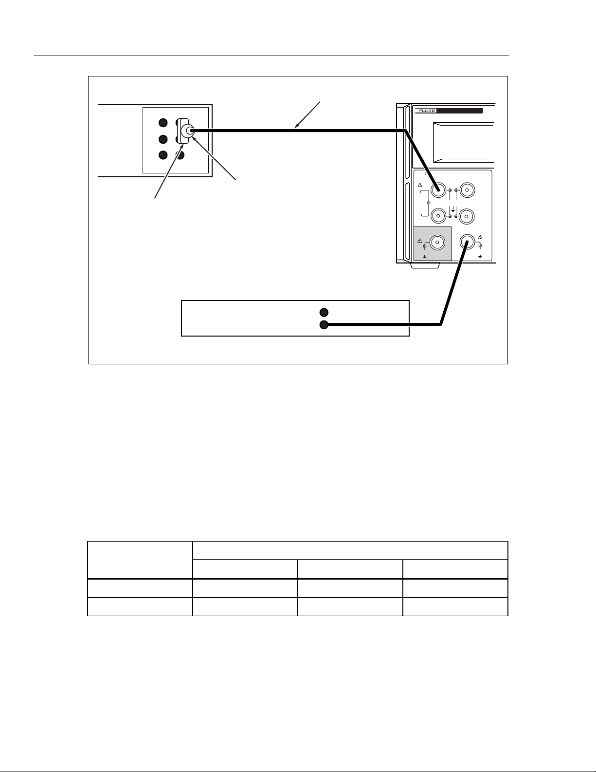
5820A
Service Manual
5820A Cable
50 Ω Feedthrough
Termination
BNC(F) to
Double Banana
Adapter
HP 3458A (Rear)
Figure 3-1. Setup for Scope Calibrator Voltage Square Wave Measurements
CAT
EXT TRIG
130V
PK
MAX
SOURCE
30V DC
MAX
MEASURE
CHAN 1-5
AUX
INPUT
20V PK
MAX
5820AHP 3458A (Front)
OSCILLOSCOPE
5820A
CALIBRATOR • 2GHz
SOURCE/MEASURE
CHAN 1
20V PK
MAX
CHAN 3
CHAN 2
CHAN 4
EXT TRIG
CHAN 5
20V PK
MAX
CHAN 2
CHAN 4
yu054f.eps
3-7. Setup for Scope Calibrator Edge and Wave Gen Square Wave
Measurements
The setup to measure the topline and baseline of Edge and Wave Generator signals
differs slightly from the Voltage Square Wave method described above. The HP 3458A
is triggered by a change in input level instead of an external trigger. The trigger level is
set to 1% of the DCV range, with ac coupling of the trigger signal. The delay after the
trigger event is also changed for the Edge and Wave Generator functions. See Table 3-2.
Refer to Figure 3-2 for the proper equipment connections.
Table 3-3. Edge and Wave Generator HP3458A Settings
HP 3458A Settings
Input Frequency NPLC DELAY (topline) DELAY (baseline)
1 kHz .01 .0002 s .0007 s
10 kHz .001 .00002 s .00007 s
3-8
Page 47

Calibration and Verification
DC Voltage Calibration
3
CAT
EXT TRIG
130V
PK
MAX
SOURCE
30V DC
MAX
MEASURE
CHAN 1-5
AUX
INPUT
20V PK
MAX
5820AHP 3458A
OSCILLOSCOPE
5820A
CALIBRATOR • 2GHz
SOURCE/MEASURE
CHAN 1
20V PK
MAX
CHAN 3
CHAN 2
CHAN 4
EXT TRIG
CHAN 2
CHAN 4
CHAN 5
20V PK
MAX
5820A Cable
50 Ω Feedthrough
Termination
BNC(F) to
Double Banana
Adapter
Figure 3-2. Setup for Scope Calibrator Edge and Wave Gen Square Wave Measurements
For all measurements, the HP 3458A is in DCV, manual ranging, with level triggering
enabled. A convenient method to make these measurements from the HP 3458A’s front
panel is to program these settings into several of the user defined keys on its front panel.
For example, to make topline measurements at 1 kHz, you would set the DMM to
“NPLC .01; LEVEL 1; DELAY .0002; TRIG LEVEL”. To find the average of multiple
readings, you can program one of the keys to “MATH OFF; MATH STAT” and then use
the “RMATH MEAN” function to recall the average or mean value.
yu055f.eps
3-8. DC Voltage Calibr ation
This procedure uses the following equipment:
• Hewlett-Packard 3458A Digital Multimeter
• BNC(f) to Double Banana adapter
• N to BNC cable supplied with the Scope Calibrator
Calibrating dc voltage requires ac voltage calibration.
When dc voltage calibration is started, the calibrator uses a special
configuration of WAVEGEN mode (with a zero frequency, ordinarily
undefined) to source approximately 3 Vdc. After the operator enters the
true dc value, this value is then transferred to the internal DACs and A/D
through a series of internal calibration steps. On firmware version 1.5 and
earlier, the output displayed is 6 V-pp @ 0.00 Hz at this step. This is a
side-effect of the special configuration used. As of firmware version 1.6,
the output display indicates 3 V @ 0.00 Hz.
Set the Calibrator to Cal DCV by pressing the SETUP, CAL and 5820A CAL blue
softkeys then follow these steps to calibrate dc voltage.
Note
Note
3-9
Page 48

5820A
Service Manual
1. Connect the Calibrator Mainframe’s CHAN 1 connector to the HP 3458A input,
using the N to BNC cable and the BNC(f) to Double Banana adapter.
2. Set the HP 3458A to DCV, Auto Range, NPLC = 10, FIXEDZ = on.
3. Press the GO ON blue softkey.
4. Ensure the HP 3458A reading is 0.0 V dc ± 10 µV. If not, adjust R121 on A41 (see
“Hardware Adjustments” in this chapter.)
5. Press the GO ON blue softkey.
6. Calibration voltages 33 V and greater will automatically put the Calibrator
Mainframe output in standby. When this occurs, press on the Calibrator
Mainframe to activate the output. Allow the HP 3458A dc voltage reading to
stabilize. Enter the reading via the Calibrator Mainframe front panel keypad, then
press ENTER.
Note
The Calibrator Mainframe will warn when the entered value is out of
bounds. If this warning occurs, recheck the setup and carefully re-enter the
µ
reading insuring proper multiplier (i.e., m,
, n, p). If the warning still
occurs, repair may be necessary.
7. Repeat steps 6 until the Calibrator Mainframe display indicates that the next steps
calibrate ac Voltage. Press the STORE CONSTS blue softkey to store the new
calibration constants.
AC Voltage must now be calibrated. Continue with the next section.
3-9. AC Voltage Calibr ation
This procedure uses the same equipment and setup as dc voltage calibration. DC
voltages are measured and entered in the Calibrator Mainframe to calibrate the AC
Voltage function.
Set up the Calibrator Mainframe to Cal ACV. Press the NEXT SECTION blue softkey
until the display reads “The next steps calibrate Scope Calibrator ACV”. Then follow
these steps to calibrate ac voltage.
1. Press the GO ON blue softkey.
2. Allow the HP 3458A dc voltage reading to stabilize. Enter the reading via the
Calibrator Mainframe front panel keypad, then press ENTER.
The Calibrator Mainframe will warn when the entered value is out of
bounds. If this warning occurs recheck the setup and carefully re-enter the
reading insuring proper multiplier (i.e., m, u, n, p). If the warning still
occurs, repair may be necessary.
Note
3-10
3. Repeat step 2 until the Calibrator Mainframe display indicates that the next steps
calibrate WAVEGEN. Press the STORE CONSTS blue softkey to store the new
calibration constants.
Page 49

3-10. DC Measurement Calibration
This procedure uses the following equipment:
• 5520A calibrator
To set 5820A to the Voltage Measurement Calibration mode, select the CAL,
MORE CAL, and MEAS V CAL blue softkeys.
1. Using the N to BNC cable, connect the CHAN 1 connector on the Calibrator
Mainframe to the Fluke 5520A Calibrator voltage binding posts using a BNC to
banana connector.
2. Set the Fluke 5520A Calibrator to 6 Vdc (Operate).
3. Enter the actual Fluke 5520A Calibrator output.
4. When prompted by the Calibrator Mainframe, set the Fluke 5520A Calibrator to
-6 Vdc (Operate).
5. Enter the actual Fluke 5520A Calibrator output.
The Calibrator Mainframe will display that the calibration is complete. Press the
STORE CONST blue softkey to store the new calibration constants.
Calibration and Verification
DC Measurement Calibration
3
3-11. Current Calibration
These procedures use the following equipment:
• Hewlett-Packard 3458A Digital Multimeter with cable
• 10 Ω, 100 Ω, and 1000 Ω precision resistor assemblies
Set the Calibrator Mainframe in CURRENT CAL mode. Remove the front panel
Current Loop using the 2 mm hex head driver and proceed with the following
procedures.
3-12. DC Current Calibrati on
1. Set the DMM to measure dc current.
2. Connect the DMM directly to the vacant banana jacks.
3. Take dc current measurements at 110 µA, 1.10 mA and 11.0 mA and enter the values
on the Calibrator front panel.
4. Press the GO ON blue softkey to proceed through the calibration points.
5. Follow the procedures on the front panel until the display reads “900 µA 1000 Hz”.
3-13. AC Current Calibrati on
For the ac calibration, the offset from 0 mA current (called the baseline) is measured and
stored in the Calibrator. Remove the DMM direct connection and set up the DMM to
measure dc volts. Follow the instructions in the section “Setup for Scope Calibrator
Voltage AC Current Measurements” above for setting up the DMM.
1. Plug in the 1000 Ω precision resistor into the Calibrator front panel.
2. Attach the DMM to the ends of the precision resistor.
3. Take voltage measurement across the resistor at 900 µA, convert to mA, and enter
the DMM value on the Calibrator front panel.
4. Press the GO ON blue softkey.
3-11
Page 50

5820A
Service Manual
5. Plug in the 100 Ω precision resistor into the Calibrator front panel.
6. Take voltage measurement across the resistor at 9.00 mA, convert to mA, and enter
the DMM value on the Calibrator front panel.
7. Press the GO ON blue softkey.
8. Plug in the 10 Ω precision resistor into the Calibrator front panel.
9. Take voltage measurement across the resistor at 90.0 mA, convert to mA, and enter
the DMM value on the Calibrator front panel.
10. Press the GO ON blue softkey.
11. To complete the Current calibration, press the STORE CONSTS blue softkey to
store the new calibration constants.
Note
The Calibrator Mainframe will warn when the entered value is out of
bounds. If this warning occurs, check the setup again and carefully reenter the reading insuring proper multiplier (i.e., m, µ, n, p). If the warning
still occurs, repair may be necessary.
3-14. Wave Generator Calibration
This procedure uses the following equipment:
• Hewlett-Packard 3458A Digital Multimeter
• BNC(f) to Double Banana adapter
• N to BNC cable supplied with the Scope Calibrator
Within the calibration menu, press the NEXT SECTION blue softkey until the display
reads “WAVEGEN Cal:”. Then follow these steps to calibrate the Wave Generator:
1. Connect the Calibrator Mainframe’s CHAN 1 connector to the HP 3458A input,
using the N to BNC cable and the BNC(f) to Double Banana adapter.
2. Set the HP 3458A to DCV, NPLC = .01, LEVEL 1, TRIG LEVEL, and the DELAY
to .0002 for measuring the upper part of the wave form (i.e. topline), and the
DELAY to .0007 for measuring the lower part of the wave form (i.e. baseline).
Manually range lock the HP 3458A to the range that gives the most resolution for
the topline measurements. Use this same range for the corresponding baseline
measurements at each step.
3. For each calibration step, take samples for at least two seconds, using the HP 3458A
MATH functions to retrieve the average or mean value. See “Setup for Scope
Calibrator Edge and Wave Generator Measurements” for more details.
3-15. Edge Amplitude Calibration
This procedure uses the following equipment:
3-12
• Hewlett-Packard 3458A Digital Multimeter
• BNC(f) to Double Banana adapter
• N to BNC cable supplied with the Scope Calibrator
• 50 Ω feedthrough termination
Page 51

Calibration and Verification
Leveled Sine Wave Amplitude Calibration
Press the NEXT SECTION blue softkey until the display reads “Set up to measure fast
edge amplitude”. Then follow these steps to calibrate edge amplitude:.
1. Connect the Calibrator Mainframe’s CHAN 1 connector to the HP 3458A input,
using the N to BNC cable and the BNC(f) to Double Banana.
2. Set the HP 3458A to DCV, NPLC = .01, LEVEL 1, TRIG LEVEL, and the DELAY
to .0002 for measuring the upper part of the wave form (i.e. topline), and the
DELAY to .0007 for measuring the lower part of the wave form (i.e. baseline).
Manually lock the HP 3458A to the range that gives the most resolution for the
baseline measurements. Use this same range for the corresponding baseline
measurements at each step. Note that in the EDGE function, the topline is very near
0 V, and the baseline is a negative voltage.
3. For each calibration step, take samples for at least two seconds, using the HP 3458A
MATH functions to enter the average or mean value. See “Setup for Scope
Calibrator Edge and Wave Generator Measurements” for more details.
The “true amplitude” of the wave form is the difference between the topline and baseline
measurements, correcting for the load resistance error. To make this correction, multiply
the readings by (0.5 * (50 + Rload)/Rload), where Rload = actual feedthrough
termination resistance.
3
3-16. Leveled Sine Wave Amplitude Calibration
This procedure uses the following equipment:
• HP 437A Power Meter or equivalent
• HP 8481D Power Sensor
• HP 8482A Power Sensor
• N (female) to BNC (female) adapter
• N to BNC cable supplied with the Scope Calibrator
Select the NEXT SECTION blue softkey until the display reads “Set up to measure
leveled sine amplitude”. Then follow these steps to calibrate Leveled Sine Wave
amplitude.
1. Connect the N to BNC cable to the Calibrator Mainframe’s CHAN 1 connector.
Connect the other end of the N to BNC cable to the 50 Ω feedthrough termination
then to the 5790A INPUT 2 using the BNC(f) to Double Banana adapter. Refer to
Figure 3-3 for the proper equipment connections.
2. Set the 5790A to AUTORANGE, digital filter mode to FAST, restart fine, and Hi
Res on.
3. Press the GO ON blue softkey.
4. Press to activate operating mode on the Calibrator Mainframe.
5. Allow the 5790A rms reading to stabilize. Multiply the 5790A reading by (0.5 * (50
+ Rload) / Rload), where Rload = the actual feedthrough termination resistance, to
correct for the resistance error. Enter the corrected rms reading via the Calibrator
Mainframe front panel keypad, then press ENTER.
3-13
Page 52

5820A
Service Manual
Note
The Calibrator Mainframe will warn when the entered value is out of
bounds. If this warning occurs recheck the setup and calculation and
carefully re-enter the corrected rms reading insuring proper multiplier
(i.e., m, u, n, p). If the warning still occurs, repair may be necessary.
6. Repeat step 5 until the Calibrator Mainframe display indicates that the next steps
calibrate Leveled Sine flatness. Press the STORE CONSTS blue softkey to store the
new calibration constants.
OSCILLOSCOPE
5820A
AC MEASUREMENT
5790A
STANDARD
INPUT 1 INPUT 2
1000V RMS MAX 1000V RMS MAX
SHELL FLOATING
SHUNT
3V RMS MAX
WIDEBAND
7V RMS MAX
10V PEAK
SHELL FLOATING
10V PK
MAX
HI
LO
MAX
GUARDGROUND
SHUNT
INPUT1
INPUT1 INPUT1 INPUT1
2.2 mV 22 mV 220 mV
2.2 V 22 V 220 mV
6789
7 mV 70 mV 700 mV
7V 70V 700V
012 345
UTIL
VIEW
SPEC
MENUS
.
+/-
1kV 2.2 mV
ENTER
REF
DELETE
CLEAR
AUTO
MAN
POWER
I
O
CALIBRATOR • 2GHz
CAT
SOURCE/MEASURE
EXT TRIG
CHAN 1
CHAN 2
PK
MAX
20V PK
SOURCE
CHAN 3
30V DC
MAX
MEASURE
CHAN 1-5
AUX
INPUT
20V PK
MAX
789
MAX
CHAN 4
456
CHAN 4
123
CHAN 5
EXT TRIG
+
0•
/
20V PK
MAX
OPR
VOLT EDGE LEVSINE MARKER
STBY
CHAN 2
130V
µ
m
k sec
M
PREV
MENU
NEW
V
REF
MORE
dBm
n
MODES
CHAN
Hz
MULTxDIV
ENTER
EDIT
RESET
CE
FIELD
SETUP
AUX
INPUT
÷
I
O
Figure 3-3. Connecting the Calibrator Mainframe to the 5790A AC Measurement Standard
3-17. Leveled Sine Wave Flatness Calibration
Leveled Sine Wave flatness calibration is divided into two frequency bands: 50 kHz to
10 MHz (low frequency) and >10 MHz to 600 MHz (high frequency). The equipment
setups are different for each band. Flatness calibration of the low frequency band is
made relative to 50 kHz. Flatness calibration of the high frequency band is made relative
to 10 MHz.
Leveled Sine Wave flatness is calibrated at multiple amplitudes. Both low and high
frequency bands are calibrated at each amplitude. Calibration begins with the low
frequency band, then the high frequency band for the first amplitude, followed by the
low frequency band, then the high frequency band for the second amplitude, and so on,
until the flatness calibration is complete.
Press the NEXT SECTION blue softkey until the display reads “Set up to measure
leveled sine flatness”.
3-18. Low Frequency Calibrati on
Connect the Calibrator Mainframe CHAN 1 connector to the 5790A WIDEBAND input
as described under “Equipment Setup for Low Frequency Flatness”.
Follow these steps to calibrate low frequency Leveled Sine Wave flatness for the
amplitude being calibrated.
yu034f.eps
3-14
1. Press the GO ON blue softkey.
2. Establish the 50 kHz reference:
• Allow the 5790A rms reading to stabilize.
Page 53

• Press the 5790A Set Ref blue softkey. (Clear any previous reference by pressing
the 5790A Clear Ref blue softkey prior to setting the new reference if required.)
3. Press the GO ON blue softkey.
4. Adjust the amplitude using the Calibrator Mainframe front panel knob until the
5790A reference deviation matches the 50 kHz reference within 1000 ppm.
5. Repeat steps 1 to 4 until the Calibrator Mainframe display indicates that the
reference frequency is now 10 MHz. Continue with the high frequency calibration.
3-19. High Frequency Calibrati on
Connect the Calibrator Mainframe CHAN 1 connector to the power meter and power
sensor as described under “Equipment Setup for High Frequency Flatness”.
Follow these steps to calibrate high frequency Leveled Sine Wave flatness for the
amplitude being calibrated.
1. Press the GO ON blue softkey.
2. Establish the 10 MHz reference:
• Press the power meter SHIFT key, then FREQ key and use the arrow keys to
enter the power sensor’s 10 MHz Cal Factor. Ensure that the factor is correct,
then press the power meter ENTER key.
Calibration and Verification
Pulse Width Calibration
3
• Allow the power meter reading to stabilize.
• Press the Power meter REL key.
3. Press the GO ON blue softkey.
4. Press the power meter SHIFT key, then FREQ key and use the arrow keys to enter
the power sensor’s Cal Factor for the frequency displayed on the Calibrator
Mainframe. Ensure that the factor is correct, then press the power meter ENTER
key.
5. Adjust the amplitude using the Calibrator Mainframe front panel knob until the
power sensor reading matches the 10 MHz reference within 0.1%.
6. Repeat steps 1 to 5 until the Calibrator Mainframe display indicates that either the
reference frequency is now 50 kHz or that the next steps calibrate pulse width.
Repeat the low frequency calibration procedure for the next amplitude unless the
Calibrator Mainframe display indicates that the next steps calibrate pulse width.
Press the STORE CONSTS blue softkey to store the new calibration constants.
3-20. Pulse Width Calibration
This procedure uses the following equipment:
• High Frequency Digital Storage Oscilloscope: Tektronix 11801 with Tektronix SD-
22/26 sampling head
• 3 dB attenuator, 3.5 mm (m/f)
• BNC(f) to 3.5 mm(m) adapter (2)
• 2 N to BNC cables supplied with the Scope Calibrator
Press the NEXT SECTION blue softkey until the display reads “Set up to measure
Pulse Width”. Then follow these steps to calibrate pulse width:
1. Connect the N to BNC cable supplied with the Scope Calibrator to the Calibrator
Mainframe’s CHAN 1 connector. Connect the other end of the N to BNC cable to
3-15
Page 54

5820A
Service Manual
one BNC(f) to 3.5 mm(m) adapter then to the DSO’s sampling head through the 3
dB attenuator.
2. Using the second BNC(f) to 3.5 mm(m) adapter and N to BNC cable, connect the
Calibrator Mainframe’s TRIG OUT connector to the 11801’s Trigger Input.
3. Set the DSO to these parameters:
• Main Time Base position (initial):40 ns
• Vertical scale: 200 mV/div, +900 mV offset
• Trigger: source = ext; level = 0.5 V; ext atten = x10; slope = +;
mode = auto
• Measurement Function: positive width
4. Press the GO ON blue softkey.
5. Adjust the DSO horizontal scale and main time base position until the pulse signal
spans between half and the full display. If no pulse is output, increase the pulse
width using the Calibrator Mainframe front panel knob until a pulse is output.
6. If prompted to adjust the pulse width by the Calibrator Mainframe display, adjust the
pulse width to as close to the displayed value as possible using the Calibrator
Mainframe front panel knob, then press the GO ON blue softkey.
7. Allow the DSO width reading to stabilize. Enter the reading via the Calibrator
Mainframe front panel keypad, then press ENTER.
The Calibrator Mainframe issues a warning when the entered value is out
of bounds. If this warning occurs, recheck the setup and carefully re-enter
the reading with the proper multiplier (i.e., m, u, n, p). If the warning still
occurs, enter a value between the displayed pulse width and the previously
entered value. Keep attempting this, moving closer and closer to the
displayed pulse width, until the value is accepted. Complete the pulse width
calibration procedure. The pulse width calibration procedure must now be
repeated until all entered values are accepted the first time without
warning.
8. Repeat steps 5 to 7 until the Calibrator Mainframe display prompts to connect a
resistor. Press the STORE CONSTS blue softkey to store the new calibration
constants.
3-21. MeasZ Calibration
The MeasZ function is calibrated using resistors and capacitors of known values. The
actual resistance and capacitance values are entered while they are being measure by the
Calibrator Mainframe.
The resistors and capacitor must make a solid connection to a BNC(f) to enable a
connection to the end of the N to BNC cable supplied with the Scope Calibrator. The
resistance and capacitance values must be known at this BNC(f) connector. Fluke uses a
HP 3458A DMM to make a 4-wire ohms measurement at the BNC(f) connector to
determine the actual resistance values and an HP 4192A Impedance Analyzer at 10 MHz
to determine the actual capacitance value.
Note
3-16
This procedure uses the following equipment:
• Resistors of known values: 40 Ω, 60 Ω, 600 kΩ and 1.5 MΩ nominal
• adapters to connect resistors to BNC(f) connector
Page 55

Calibration and Verification
MeasZ Calibration
• adapters and capacitors to achieve 5 pF, 28 pF, and 50 pF nominal value at the end
of BNC(f) connector
• N to BNC cable supplied with the Scope Calibrator
5820A
OSCILLOSCOPE
5820A
CALIBRATOR • 2GHz
3
BNC(F)
5820A
Cable
CAT
EXT TRIG
130V
PK
MAX
SOURCE
30V DC
MAX
MEASURE
CHAN 1-5
AUX
INPUT
20V PK
MAX
SOURCE/MEASURE
CHAN 1
20V PK
MAX
CHAN 3
CHAN 2
CHAN 4
EXT TRIG
CHAN 2
CHAN 4
CHAN 5
20V PK
MAX
yu056f.eps
Figure 3-4. Setup for MeasZ Calibration
Set the Calibrator Mainframe in Scope Cal mode at the prompt to connect a 40 Ω
resistor. Then follow these steps to calibrate MeasZ.
1. Connect the N to BNC cable to the SCOPE connector. Connect the other end of the
N to BNC cable to the BNC(f) connector attached to the 40 Ω resistance. Refer to
Figure 3-4 for the proper equipment connections.
2. Press the GO ON blue softkey.
3. Enter the actual 40 Ω resistance.
4. When prompted by the Calibrator Mainframe, disconnect the 40 Ω resistance and
connect the 60 Ω resistance.
5. Press the GO ON blue softkey.
6. Enter the actual 60 Ω resistance.
Note
The Calibrator Mainframe will warn when the entered value is out of
bounds. If this warning occurs, recheck the setup and carefully re-enter the
actual resistance insuring proper multiplier (i.e., m, u, n, p). If the warning
still occurs, repair may be necessary.
7. When prompted by the Calibrator Mainframe, disconnect the 60 Ω resistance and
connect the 0.6 MΩ resistance to the end of the N to BNC cable.
8. Press the GO ON blue softkey.
9. Enter 0.6 MΩ resistance
10. When prompted by the Calibrator Mainframe, disconnect the 0.6 MΩ resistance and
connect the 1.5 MΩ resistance to the end of the N to BNC cable
11. Press the GO ON blue softkey.
3-17
Page 56

5820A
Service Manual
Note
Calibrating the capacitance for the Scope Calibrator uses 4 capacitors,
0 pF, 5 pF, 28 pF, and 50 pF. Starting with 0 (or no input) you proceed
through each capacitor entering the exact value each time.
12. When prompted for the first reference capacitor by the Calibrator Mainframe,
disconnect the 1.5 MΩ resistance and leave nothing attached to the end of the N to
BNC cable.
13. Press the GO ON blue softkey.
14. Enter 0.
15. When prompted by the Calibrator Mainframe, connect the 5 pF capacitor to the end
of the N to BNC cable.
16. Press the GO ON blue softkey.
17. Enter the actual 5 pF capacitance value.
18. When prompted by the Calibrator Mainframe, disconnect the 5 pF capacitor and
connect the 28 pF to the end of the N to BNC cable.
19. Press the GO ON blue softkey.
20. Enter the actual 28 pF capacitance value.
21. When prompted by the Calibrator Mainframe, disconnect the 28 pF capacitor and
connect the 50 pF to the end of the N to BNC cable.
22. Press the GO ON blue softkey.
23. Enter the actual 50 pF capacitance.
24. The Calibrator Mainframe will prompt that the calibration is complete. Press the
STORE CONSTS blue softkey to store the new calibration constants.
3-22. Leveled Sine Wave Flatness Calibration (GHz Option)
Leveled Sine Wave Flatness Calibration is only applicable if the 5820A has the GHz
Option installed. This calibration procedure uses the same equipment as in the 5820A
Leveled Sine Wave Flatness (High Frequency) calibration procedure. See the GHz
section for details.
3-23. 5820A-5 Option
The 5820A-5 Option allows you to calibrate up to five oscilloscope channels
simultaneously without changing cables. This allows you to perform fast, automated
calibrations with documented procedures and results while freeing the operator to
complete other work. You can find this option discussed throughout the manual where
appropriate.
Note
If the 5820A is equipped with the 5-channel option, the Mainframe will
indicate when to move to the next channel.
3-24. Verification
All of the Oscilloscope Calibration functions should be verified at least once per year, or
each time the Scope Calibrator is calibrated. The verification procedures in this section
provide traceable results; however the factory uses different procedures of higher
precision than those described here. The procedures in this manual have been developed
to provide users the ability to verify the Scope Calibrator at their own site if they are
3-18
Page 57

Calibration and Verification
required to do so. Fluke strongly recommends that, if possible, you return your unit to
Fluke for calibration and verification.
All equipment specified for Scope Calibrator verification must be calibrated, certified
traceable if traceability is to be maintained, and operating within their normal specified
operating environment. It is also important to ensure that the equipment has had
sufficient time to warm up prior to its use. Refer to the operating manual for each piece
of equipment for details.
Before you begin verification, you may wish to review all of the procedures in advance
to ensure you have the resources to complete them.
All of the Scope Calibrator functions are listed in Table 3-4, with the verification
technique indicated.
Table 3-4. Verification Methods for Scope Calibrator Functions
Function Verification Method
DC Voltage Procedure provided in this manual.
AC Voltage amplitude Procedure provided in this manual.
Verification
3
AC Voltage frequency Procedure provided in this manual.
DC Voltage
Measurement
Current Procedure provided in this manual.
Edge amplitude Procedure provided in this manual.
Edge frequency, duty
cycle, rise time
Tunnel Diode Pulser
amplitude
Leveled sine wave
amplitude, frequency,
harmonics, and flatness
Time marker period Procedure provided in this manual.
Wave generator
amplitude
Pulse width, period Procedure provided in this manual.
MeasZ resistance,
capacitance
Overload functionality Procedure provided in this manual.
Procedure provided in this manual.
Procedure provided in this manual.
Procedure provided in this manual. See “Voltage and Edge Calibration
and Verification” for details.
Procedures provided in this manual.
Procedure provided in this manual.
Procedure provided in this manual.
3-19
Page 58

5820A
Service Manual
3-25. DC Voltage Verifi cat ion
This procedure uses the following equipment:
• Hewlett-Packard 3458A Digital Multimeter
• BNC(f) to Double Banana adapter
• 50 Ω feedthrough termination
• N to BNC cable supplied with the
Set the Calibrator Mainframe to the Volt menu. Follow these steps to verify the wave
generator function.
3-26. Verification at 1 M
For the 1 MΩ verification, connect the Calibrator Mainframe’s CHAN 1 connector to the
HP 3458A input, using the cable and the BNC(f) to Double Banana adapter.
Make sure the Calibrator Mainframe impedance is set to 1 MΩ (The blue softkey under
Output @ toggles the impedance between 50 Ω and 1 MΩ).
1. Set the HP 3458A to DCV, Auto Range, NPLC = 10, FIXEDZ = on.
2. Program the Calibrator Mainframe to output the voltage listed in Table 3-5. Press
on the Calibrator Mainframe to activate the output.
3. Allow the HP 3458A reading to stabilize, then record the HP 3458A reading for each
voltage in Table 3-5.
4. Compare result to the tolerance column.
3-27. Verification at 50
For the 50 Ω verification, connect the CHAN 1 connector to the HP 3458A input, using
the cable and the 50 Ω termination connected to the N to BNC to Banana Plug adapter.
Make sure the Calibrator Mainframe impedance is set to 50 Ω (The blue softkey under
Output @ toggles the impedance between 50 Ω and 1 MΩ).
Scope Calibrator
Ω
Ω
3-20
1. Set the HP 3458A to DCV, Auto Range, NPLC = 10, FIXEDZ = on.
2. Program the Calibrator Mainframe to output the voltage listed in Table 3-6. Press
on the Calibrator Mainframe to activate the output.
3. Allow the HP 3458A reading to stabilize, then record the HP 3458A reading for each
voltage in Table 3-6.
4. Multiply the readings by (0.5 * (50 + Rload) / Rload), where Rload = the actual
feedthrough termination resistance, to correct for the resistance error.
Page 59

Table 3-5. DC Voltage Verification
(Into 1 MΩ Impedance Unless Noted)
Calibration and Verification
Verification
3
Nominal Value
(V dc)
0 25 µV
0.00125 25.3 µV
-0.00125 25.3 µV
0.00249 25.6 µV
-0.00249 25.6 µV
0.0025 25.6 µV
-0.0025 25.6 µV
0.00625 26.5 µV
-0.00625 26.5 µV
0.0099 27.5 µV
-0.0099 27.5 µV
0.01 27.5 µV
-0.01 27.5 µV
0.0175 29.4 µV
-0.0175 29.4 µV
0.0249 31.2 µV
-0.0249 31.2 µV
0.025 31.2 µV
-0.025 31.2 µV
0.0675 41.8 µV
-0.0675 41.8 µV
0.1099 52.5 µV
-0.1099 52.5 µV
0.11 52.5 µV
-0.11 52.5 µV
0.305 101.50 µV
-0.305 101.50 µV
0.499 150 µV
-0.499 150 µV
Measured Value
(V dc)
Deviation
(V dc) 1-Year Spec.
3-21
Page 60

5820A
Service Manual
Table 3-5. DC Voltage Verification (cont.)
Nominal Value
(V dc)
0.5 150 µV
-0.5 150 µV
1.35 362.5 µV
-1.35 362.5 µV
2.19 572 µV
-2.19 572 µV
2.2 572 µV
-2.2 572 µV
6.6 1.67 mV
-6.6 1.67 mV
10.99 2.77 mV
-10.99 2.77 mV
11 2.77 mV
-11 2.77 mV
70.5 17.65 mV
-70.5 17.65 mV
130 32.5 mV
-130 32.5 mV
6.599 (50 Ω) 16.5 mV
Measured Value
(V dc)
Table 3-6. DC Voltage Verification at 50 Ω
Deviation
(V dc) 1-Year Spec.
Calibrator
Mainframe
Output
0 mV 0.00004 V
2.49 mV 4.623E-05 V
-2.49 mV 4.623E-05 V
9.90 mV 6.475E-05 V
-9.90 mV 6.475E-05 V
24.9 mV 0.0001023 V
-24.9 mV 0.0001023 V
109.9 mV 0.0003148 V
-109.9 mV 0.0003148 V
499 mV 0.0012875 V
-499 mV 0.0012875 V
2.19 V 0.005515 V
-2.19 V 0.005515 V
6.599 V 0.0165375 V
-6.599 V 0.0165375 V
HP 3458A Rdg (V dc) Reading x Correction Tolerance (V dc)
3-22
Page 61

3-28. AC Voltage Amplit ude Veri fication
This procedure uses the following equipment:
• Hewlett-Packard 3458A Digital Multimeter
• BNC(f) to Double Banana adapter
• 50 Ω feedthrough termination
• N to BNC cable supplied with the Scope Calibrator
• N to BNC cable to connect the Calibrator Mainframe TRIG OUT to the HP 3458A
Ext Trig
Set the Calibrator Mainframe to the Volt menu. Follow these steps to verify the ac
voltage function.
Calibration and Verification
Verification
3
3-29. Verification at 1 M
For the 1 MΩ verification, connect the Calibrator Mainframe’s CHAN 1 connector to the
HP 3458A input, using the cable supplied with the Calibrator Mainframe and the BNC(f)
to Double Banana adapter. Connect the Calibrator Mainframe TRIG OUT connector to
the HP 3458A Ext Trig connector located on the rear of that instrument.
Make sure the Calibrator Mainframe impedance is set to 1 MΩ. (The blue softkey under
Output @ toggles the impedance between 50 Ω and 1 MΩ.)
1. When making measurements at 1 kHz, set the HP 3458A to DCV, NPLC = .01,
TRIG EXT, and the DELAY to .0007 for measuring the topline of the wave form,
and the DELAY to .0012 for measuring the baseline of the wave form. Manually
lock the HP 3458A to the range that gives the most resolution for the topline
measurements. Use this same range for the corresponding baseline measurements at
each step.
2. Enable the Calibrator Mainframe external trigger by toggling the blue softkey under
TRIG to /1.
3. Measure the topline first, as indicated in Table 3-7. For each measurement, take
samples for at least two seconds, using the HP 3458A MATH functions to determine
the average or mean value.
4. Measure the baseline of each output after the corresponding topline measurement, as
indicated in Table 3-7. The peak-to-peak value is the difference between the topline
and baseline measurements. Compare the result to the tolerance column.
Ω
5. When making measurements at the other frequencies, set up the HP 3458A (NPLC
and topline and baseline DELAY) per Table 3-2.
3-23
Page 62

5820A
Service Manual
Nominal Value
Table 3-7. AC Voltage Amplitude Verification
(Into 1 MΩ Impedance Unless Noted)
(V p-p)
0.001 1000 5.5 µV
-0.001 1000 5.5 µV
0.025 1000 17.5 µV
-0.025 1000 17.5 µV
0.11 1000 60 µV
-0.11 1000 60 µV
0.5 1000 255 µV
-0.5 1000 255 µV
2.2 1000 1.1 mV
-2.2 1000 1.1 mV
11 1000 5.5 mV
-11 1000 5.5 mV
130 1000 6.5 mV
-130 1000 6.5 mV
Frequency
(Hz)
Measured Value
(V p-p)
Deviation
(V p-p)
1-year Spec.
(V p-p)
3-30. Verification at 50
For the 50 Ω verification, connect the Calibrator Mainframe’s CHAN 1 connector to the
HP 3458A input, using the cable supplied with the Calibrator Mainframe, the external 50
Ω termination, and the BNC(f) to Double Banana adapter. (The 50 Ω termination is
closest to the HP 3458A input.) Connect the Calibrator Mainframe TRIG OUT
connector to the HP 3458A Ext Trig connector located on the rear of that instrument.
Make sure the Calibrator Mainframe impedance is set to 50 Ω. (The blue softkey under
Output @ toggles the impedance between 50 Ω and 1 MΩ). Proceed with the following
steps:
1. Set the HP 3458A to DCV, NPLC = .01, TRIG EXT, and the DELAY to .0007 for
measuring the topline of the wave form, and the DELAY to .0012 for measuring the
baseline of the wave form. Manually lock the HP 3458A to the range that gives the
most resolution for the topline measurements. Use this same range for the
corresponding baseline measurements at each step. See Table 3-8.
2. Enable the Calibrator Mainframe external trigger by toggling the blue softkey under
TRIG to /1.
3. Measure the topline first, as indicated in Table 3-8. For each measurement, take
samples for at least two seconds, using the HP 3458A MATH functions to determine
the average or mean value.
4. Measure the baseline of each output after the corresponding topline measurement, as
indicated in Table 3-8. The peak-to-peak value is the difference between the topline
and baseline measurements. Compare the result to the tolerance column.
Ω
3-24
Page 63

Calibration and Verification
Table 3-8. AC Voltage Verification at 50 Ω
Calibrator
Mainframe
Output
(1 kHz)
1 mV 100 mV dc 0.000043
-1 mV 100 mV dc 0.000043
10 mV 100 mV dc 0.000065
-10 mV 100 mV dc 0.000065
25 mV 100 mV dc 0.000103
-25 mV 100 mV dc 0.000103
110 mV 100 mV dc 0.000315
-110 mV 100 mV dc 0.000315
500 mV 1 V dc 0.00129
HP 3458A
Range
Topline
Reading
Baseline
Reading Peak-to-Peak
Peak-to-Peak x
Correction
Tolerance
(±V)
Verification
3
-500 mV 1 V dc 0.00129
2.2 V 10 V dc 0.00554
-2.2 V 10 V dc 0.00554
6.6 V 10 V dc 0.01654
-6.6 V 10 V dc 0.01654
3-31. AC Voltage Frequency Verifi cat ion
This procedure uses the following equipment:
• PM 6680 Frequency Counter with an ovenized timebase (Option PM 9690 or PM
9691)
• N to BNC cable supplied with the Scope Calibrator
Refer to Figure 3-5 for the proper equipment connections.
3-25
Page 64

5820A
Service Manual
5820A Cable
5820A
OSCILLOSCOPE
5820A
CALIBRATOR • 2GHz
At 50 MHZ
PM 6680A
CAT
EXT TRIG
130V
PK
MAX
SOURCE
30V DC
MAX
MEASURE
CHAN 1-5
AUX
INPUT
20V PK
MAX
SOURCE/MEASURE
CHAN 1
20V PK
MAX
CHAN 3
CHAN 2
CHAN 4
EXT TRIG
20V PK
Figure 3-5. Setup for AC Voltage Frequency Verification
Set the Calibrator Mainframe to the Volt menu. Press on the Calibrator Mainframe
to activate the output. Then follow these steps to verify ac voltage frequency.
1. Set the PM 6680’s FUNCTION to measure frequency on channel A with auto
trigger, measurement time set to 1 second or longer, 1MΩ impedance, and filter off.
2. Using the N to BNC cable, connect the CHAN 1 connector on the Calibrator
Mainframe to PM 6680 channel A.
3. Program the Calibrator Mainframe to output 2.1 V at each frequency listed in Table
3-9.
4. Allow the PM 6680 reading to stabilize, then record the PM 6680 reading for each
frequency listed in Table 3-9. Compare to the tolerance column of Table 3-9.
CHAN 2
CHAN 4
CHAN 5
MAX
yu057f.eps
3-26
Table 3-9. AC Voltage Frequency Verification
Calibrator Mainframe
Frequency
(Output @ 2.1 V p-p)
PM 6680 Reading
(Frequency) Tolerance
10 Hz 3.3 E
100 Hz 33 E
1 kHz 330 E
10 kHz 3,300 E
3-32. DC Measurement Verifi cat i on
This procedure uses the following equipment:
• Fluke 5520A Calibrator
1. Select Voltage Measurement mode.
-6
-6
-6
-6
Page 65

Calibration and Verification
2. Using the N to BNC cable, connect the CHAN 1 connector on the Calibrator
Mainframe to the Fluke 5520A Calibrator voltage binding posts using a BNC to
banana connector.
Record the 5820A reading for each voltage in Table 3-10.
Table 3-10. DC Voltage Measurement Verification
Verification
3
Nominal Value
(V dc)
0 V 0.001
1 V 0.0015
2.5 V 0.00225
5 V 0.0035
6.5 V 0.02625
9.9 V 0.03475
-1 V 0.0015
-2.5 V 0.00225
-5 V 0.0035
-6.5 V 0.02625
-9.9 V 0.03475
3-33. Current Verificati on
This procedure uses the following equipment:
Measured Value Deviation
1-year Spec.
(V p-p)
• Hewlett-Packard 3458A Digital Multimeter with cable
• 1 Ω, 10 Ω, 100 Ω, and 1000 Ω precision resistor assemblies
Remove the front panel Current Loop using the 2 mm hex head driver.
3-34. DC Current Ver if icat ion
1. Connect the DMM directly to the vacant banana jacks on the calibrator.
2. Program the Calibrator Mainframe to output the Currents listed in Table 3-11. Press
on the Calibrator Mainframe to activate the output.
3. Allow the HP 3458A reading to stabilize, then record the HP 3458A reading for each
current in Table 3-11.
4. Compare result to the tolerance column.
3-27
Page 66

5820A
Service Manual
Table 3-11. DC Current Verification
Calibrator Mainframe
output
0.100 mA 0.000750
-0.100 mA 0.000750
0.550 mA 0.001875
-0.550 mA 0.001875
1.099 mA 0.003248
-1.099 mA 0.003248
1.100 mA 0.003250
-1.100 mA 0.003250
5.50 mA 0.014250
-5.50 mA 0.014250
10.99 mA 0.027975
-10.99 mA 0.027975
11.00 mA 0.028000
-11.00 mA 0.028000
50.00 mA 0.125500
-50.00 mA 0.125500
100.0 mA 0.250500
-100.0 mA 0.250500
HP 3458A Reading
(mA dc)
Tolerance (mA dc)
3-35. AC Current Verificat ion
The setup to measure the topline and baseline of ac current uses the HP 3458A triggered
by a change in input level (see Table 3-12 for HP3458A settings). The trigger level is set
to 1% of the DCV range, with ac coupling of the trigger signal. Connect the precision
resistor assemblies, as indicated, to the banana jacks on the front panel. Connect the
DMM to the precision resistor. Set the HP 3458A to DCV, Auto Range, NPLC = 10,
FIXEDZ = on. Use the same delays and settings used in the section “AC Current
Calibration”. Record the HP3458A readings in Table 3-13.
Table 3-12. AC Measurement HP3458A Settings
HP 3458A Settings
Input Frequency NPLC DELAY (topline) DELAY (baseline)
45 Hz .01 .0002 s .012
500 Hz .01 .0002 s .0012 s
1 kHz .01 .0002 s .0005 s
3-28
Page 67

Calibration and Verification
Verification
Table 3-13. AC Current Verification
Actual
Resistor
Nominal Output
Current @
Resistance Value
0.10 mA @ 1k Ω 45 Ω 0.000750
-0.10 mA@ 1k Ω 45 0.000750
0.10 mA@ 1k Ω 500 0.000750
-0.10 mA@ 1k Ω 500 0.000750
0.10 mA@ 1k Ω 1000 0.000750
-0.10 mA@ 1k Ω 1000 0.000750
1.099 mA @ 100 Ω 45 0.003248
-1.099 mA @ 100 Ω 45 0.003248
1.099 mA @ 100 Ω 500 0.003248
Frequency
(Hz)
Value
0.05% (W)
A
Topline
Reading
(Vdc)
B
Baseline
Reading
(Vdc)
C
Calculated
Current
(B-C) ÷ A
(mA)
D
Error
D - Nom
Tolerance
(±mA)
3
-1.099 mA @ 100 Ω 500 0.003248
1.099 mA@ 100 Ω 1000 0.003248
-1.099 mA@ 100 Ω 1000 0.003248
1.10 mA@ 100 Ω 45 0.003250
-1.10 mA@ 100 Ω 45 0.003250
1.10 mA@ 100 Ω 500 0.003250
-1.10 mA@ 100 Ω 500 0.003250
1.10 mA@ 100 Ω 1000 0.003250
-1.10 mA@ 100 Ω 1000 0.003250
10.99 mA@ 10 Ω 45 0.027975
-10.99 mA@ 10 Ω 45 0.027975
10.99 mA@ 10 Ω 500 0.027975
-10.99 mA@ 10 Ω 500 0.027975
10.99 mA@ 10 Ω 1000 0.027975
-10.99 mA@ 10 Ω 1000 0.027975
11.00 mA@ 10 Ω 45 0.028000
-11.00 mA@ 10 Ω 45 0.028000
11.00 mA@ 10 Ω 500 0.028000
-11.00 mA@ 10 Ω 500 0.028000
11.00 mA@ 10 Ω 1000 0.028000
3-29
Page 68

5820A
Service Manual
3-36. Edge Amplitude Verif i cation
For the edge amplitude verification, connect the Calibrator Mainframe’s CHAN 1
connector to the HP 3458A input, using the cable supplied with the Calibrator
Mainframe, the external 50 Ω termination, and the BNC(f) to double banana adapter.
(The 50 Ω termination is closest to the HP 3458A input.)
1. For measurements of a 1 kHz signal, set the HP 3458A to DCV, NPLC = .01,
LEVEL 1, TRIG LEVEL, and the DELAY to .0002 for measuring the upper part of
the wave form (i.e. topline), and the DELAY to .0007 for measuring the lower part
of the wave form (i.e. baseline). For measurements of a 10 kHz signal, set the HP
3458A to DCV, NPLC = .001, LEVEL 1, TRIG LEVEL, and the DELAY to .00002
for measuring the topline, and the DELAY to .00007 for measuring the baseline.
2. Manually lock the HP 3458A to the range that gives the most resolution for the
baseline measurements. Use this same range for the corresponding baseline
measurements at each step. Note that in the EDGE function, the topline is very near
0 V, and the baseline is a negative voltage. See Table 3-14.
3. For each calibration step, take samples for at least two seconds, using the HP 3458A
MATH functions to enter the average or mean value.
4. The peak-to-peak value of the wave form is the difference between the topline and
baseline measurements, correcting for the load resistance error. To make this
correction, multiply the readings by (0.5 * (50 + Rload)/Rload), where Rload =
actual feedthrough termination resistance. Record each reading as indicated in Table
3-14.
Table 3-14. Edge Amplification Verification
Calibrator
Mainframe Edge
Output
100 mV, 1 kHz 100 mV dc 0.0022
1.00V, 1 kHz 1 V dc 0.0202
5 mV, 10 kHz 100 mV dc 0.0003
10 mV, 10 kHz 100 mV dc 0.0004
25 mV, 10 kHz 100 mV dc 0.0007
50 mV, 10 kHz 100 mV dc 0.0012
100 mV, 10 kHz 1 V dc 0.0022
500 mV, 10 kHz 1 V dc 0.0102
1.00 V, 10 kHz 1 V dc 0.0202
2.5 V, 10 kHz 10 V dc 0.0502
HP 3458A
Range
Topline
Reading
Baseline
Reading
Peak-to-
Peak
Peak-to-
Peak x
Correction
Tolerance
3-37. Edge Frequency Verificati on
This procedure uses the following equipment:
• PM 6680 Frequency Counter with an ovenized timebase (Option PM 9690 or PM
9691)
(±V)
3-30
• N to BNC cable supplied with the Scope Calibrator
Page 69

Calibration and Verification
Set the Calibrator Mainframe to the Edge menu. Press on the Calibrator
Mainframe to activate the output. Then follow these steps to verify Edge frequency.
1. Set the PM 6680’s FUNCTION to measure frequency on channel A with auto
trigger, measurement time set to 1 second or longer, 50 Ω impedance, and filter off.
2. Using the N to BNC cable, connect the CHAN 1 connector on the Calibrator
Mainframe to PM 6680 channel A.
3. Program the Calibrator Mainframe to output 2.5 V at each frequency listed in Table
3-15.
4. Allow the PM 6680 reading to stabilize, then record the PM 6680 reading for each
frequency listed in Table 3-15. Compare to the tolerance column of Table 3-15.
Table 3-15. Edge Frequency Verification
Calibrator Mainframe
Frequency
(Output @ 2.5 V p-p)
1 kHz .001 Hz
PM 6680 Reading
(Frequency) Tolerance
Verification
3
10 kHz 0.01 Hz
100 kHz 0.1 Hz
1 MHz 1 Hz
10 MHz 10 Hz
3-38. Edge Duty Cycle Verifi cat ion
This procedure uses the following equipment:
• PM 6680 Frequency Counter
• N to BNC cable supplied with the Scope Calibrator
Set the Calibrator Mainframe to the Edge menu. Press on the Calibrator
Mainframe to activate the output. Then follow these steps to verify Edge duty cycle.
1. Set the PM 6680’s FUNCTION to measure duty cycle on channel A with auto
trigger, measurement time set to 1 second or longer, 50 Ω impedance, and filter off.
2. Using the N to BNC cable, connect the CHAN 1 connector on the Calibrator
Mainframe to PM 6680 channel A.
3. Program the Calibrator Mainframe to output 2.5 V at 1 MHz.
4. Allow the PM 6680 reading to stabilize. Compare the duty cycle reading to 50% ±
5%.
3-39. Edge Rise Time Verifi cat ion
This procedure tests the edge function’s rise time. Aberrations are also checked with the
Tektronix 11801 oscilloscope and SD-22/26 sampling head.
The following equipment is used to verify the edge rise time:
• High Frequency Digital Storage Oscilloscope: Tektronix 11801 with Tektronix SD-
22/26 sampling head
• 3 dB attenuator, 3.5 mm (m/f)
3-31
Page 70

5820A
Service Manual
• BNC(f) to 3.5 mm(m) adapter (2)
• N to BNC cable supplied with the Scope Calibrator
• second N to BNC cable
Connect the N to BNC cable supplied with the Scope Calibrator to the Calibrator
Mainframe’s CHAN 1 connector. Connect the other end of the N to BNC cable to one
BNC(f) to 3.5 mm(m) adapter then to the DSO’s sampling head through the 3 dB
attenuator. Refer to Figure 3-6 for the proper equipment connections.
Using the second BNC(f) to 3.5 mm(m) adapter and N to BNC cable, connect the
Calibrator Mainframe’s EXT TRIG (channel 5) connector to the 11801’s Trigger Input.
Tek 11801
With 5D26 Sampling Head
5820A
OSCILLOSCOPE
5820A
CALIBRATOR • 2GHz
5820A
3 dB Attenaator
3.5 mm (m/f)
Cable
CAT
EXT TRIG
130V
PK
MAX
SOURCE
30V DC
MAX
MEASURE
CHAN 1-5
AUX
INPUT
20V PK
MAX
SOURCE/MEASURE
CHAN 1
20V PK
MAX
CHAN 3
CHAN 2
CHAN 4
EXT TRIG
CHAN 2
CHAN 4
CHAN 5
20V PK
MAX
BNC(F) to
3.5 mm (m)
Adapter
Figure 3-6. Setup for Edge Rise Time Verification
The Calibrator Mainframe should have the Edge menu on the display. Press on the
Calibrator Mainframe to activate the output. Press the softkey under TRIG to select the
TRIG/1 External Trigger output. Program the Calibrator Mainframe to output
250 mV @ 1 kHz. Set the DSO to these parameters:
yu058f.eps
3-32
Digital Storage Oscilloscope Setup
Main Time Base position (initial) 40 ns
Horizontal scale 500 ps/div
Measurement Function Rise Time
1. Program the Calibrator Mainframe to output the voltage and frequency listed in
Table 3-16. Press on the Calibrator Mainframe to activate the output.
2. Change the vertical scale of the DSO to the value listed in the table. Adjust the main
time base position and vertical offset until the edge signal is centered on the display.
Record the rise time measurement in column A of Table 3-16.
3. Correct the rise time measurement by accounting for the SD-22/26 sampling head’s
rise time. The SD-22/26 rise time is specified as <28 ps. Column B = sqrt((Column
2
- (SD-22/26 rise time)2).
A)
4. The edge rise time measured should be less than the time indicated in Table 3-16.
Page 71

Table 3-16. Edge Rise Time Verification
Calibration and Verification
Verification
3
Calibrator Mainframe Output
Voltage Frequency
250 mV 1 kHz 20.0 < 300 ps
250 mV 1 MHz 20.0 < 300 ps
250 mV 10 MHz 20.0 < 350 ps
500 mV 1 kHz 50.0 < 300 ps
500 mV 1 MHz 50.0 < 300 ps
500 mV 10 MHz 50.0 < 350 ps
1 V 1 kHz 100.0 < 300 ps
1 V 1 MHz 100.0 < 300 ps
1 V 10 MHz 100.0 < 350 ps
2.5 V 1 kHz 200.0 < 300 ps
2.5 V 1 MHz 200.0 < 300 ps
2.5 V 10 MHz 200.0 < 350 ps
DSO
Vertical
Axis
(mV/div)
AB
11801
Reading
Corrected
Reading Tolerance
3-40. Edge Aberrations
The following equipment is needed for this procedure:
• High Frequency Digital Storage Oscilloscope: Tektronix 11801 with Tektronix SD-
22/26 sampling head
• N to BNC output cables provided with the Scope Calibrator (2)
Before you begin this procedure, verify that the Scope Calibrator is in the edge mode
(the Edge menu is displayed), program it to output 1 V p-p @ 1 MHz, and press the soft
key under TRIG to select the TRIG/1 External Trigger output. Press to activate the
output and trigger.
Set the DSO vertical to 10 mV/div and horizontal to 10 ns/div. Next, set the signal edge
against the left side of the DSO display. Mentally note the signal amplitude 90 ns from
the edge; use this point as the reference level. It maybe helpful to set the DSO to average
4 per reading. Now set the DSO to 1 ns/div and look at the first 10 ns of the edge signal
with the rising edge at the left edge of the DSO display.
With the vertical setting, each line on the DSO represents a 1% (i.e. 10 mV) of
aberration. Determine that the Scope Calibrator falls within the typical specifications
shown in Table 3-17. For time greater than 10 ns, set the DSO to 10 ns/div. Verify the
aberrations are within specification.
Table 3-17. Edge Aberrations
Time from 50% of Rising Edge Typical Edge Aberrations
0 - 2 ns < 32 mV (3.2%)
2 - 5 ns < 22 mV (2.2%)
5 - 30 ns < 12 mV (1.2%)
> 30 ns < 7 mV (0.7%)
3-33
Page 72

5820A
Service Manual
3-41. Tunnel Diode Pulser Drive Ampl itude Verification
This procedure uses the following equipment:
• Hewlett-Packard 3458A Digital Multimeter
• BNC(f) to Double Banana adapter
• N to BNC cable supplied with the Scope Calibrator
Set the Calibrator Mainframe to Edge. Proceed with the following steps:
1. Connect the Calibrator Mainframe’s CHAN 1 connector to the HP 3458A input,
using the N to BNC cable and the BNC(f) to Double Banana adapter.
2. Activate the TD Pulser output by pushing the TDPULSE blue softkey. The output
should now be at 80 V peak-to-peak, 100 kHz, STANDBY.
3. Set the HP 3458A to DCV, NPLC = .001, LEVEL 1, TRIG LEVEL, and the DELAY
to .00012 for measuring the topline and DELAY to .00007 for measuring the
baseline. Manually range lock the HP 3458A to the 100 V dc range.
4. Change the Calibrator Mainframe output frequency to 10 kHz. Push the operate key,
and use the HP 3458A to measure the topline and baseline.
5. The peak-to-peak value is the difference between the topline and baseline. Record
these values in Table 3-18, and compare against the listed tolerance.
Table 3-18. Tunnel Diode Pulser Verification
Nominal Value
(V p-p)
11 100 0.2202
11 10000 0.2202
55 100 1.1002
55 10000 1.1002
100 100 2.0002
100 10000 2.0002
Frequency
(Hz)
Measured Value
(V p-p)
3-42. Leveled Sine Wave Amplit ude Verification
This procedure uses the following equipment:
• 5790A AC Measurement Standard
• BNC(f) to Double Banana Plug adapter
• 50 Ω feedthrough termination
• N to BNC cable supplied with the Scope Calibrator
Set the Calibrator Mainframe to the Levsine menu. Press on the Calibrator
Mainframe to activate the output. Then follow these steps to verify the leveled sine wave
amplitude.
1. Connect the N to BNC cable to the Calibrator Mainframe’s CHAN 1 connector.
Connect the other end of the N to BNC cable to the 50 Ω feedthrough termination
then to the 5790A INPUT 2 using the BNC(f) to Double Banana adapter.
Deviation
(V p-p)
1-Year Spec.
(V p-p)
3-34
2. Set the 5790A to AUTORANGE, digital filter mode to FAST, restart fine, and Hi
Res on.
3. Program the Calibrator Mainframe to output the voltage listed in Table 3-19.
Page 73

Calibration and Verification
4. Allow the 5790A reading to stabilize, then record the 5790A’s rms reading for each
voltage listed in Table 3-19.
5. Multiply the rms reading by the conversion factor of 2.8284 to convert it to the peakto-peak value.
6. Multiply the peak-to-peak value by (0.5 * (50 + Rload) / Rload), where Rload = the
actual feedthrough termination resistance, to correct for the resistance error.
Compare result to the tolerance column.
Table 3-19. Leveled Sine Wave Amplitude Verification
Calibrator
Mainframe
Output
(@ 50 kHz)
5.0 mV 400 µV
7.5 mV 450 µV
9.9 mV 498 µV
10.0 mV 500 µV
25.0 mV 800 µV
39.0 mV 1.08 mV
40.0 mV 1.10 mV
70.0 mV 1.70 mV
99.0 mV 2.28 mV
100.0 mV 2.30 mV
250.0 mV 5.30 mV
399.0 mV 8.28 mV
0.4 V 8.3 mV
0.8 V 16.3 mV
1.2 V 24.3 mV
1.3 V 26.3 V
3.4 V 68.3 mV
5.5 V 110.3 mV
5790A Reading
(V rms)
5790A Reading x
2.8284 (V p-p)
V p-p value x
Correction
Tolerance
(V p-p)
Verification
3
3-43. MHz Leveled Sine Wave Flatness Verification
Leveled Sine Wave flatness verification is divided into two frequency bands: 50 kHz to
10 MHz (low frequency) and >10 MHz to 600 MHz (high frequency). The equipment
setups are different for each band. Leveled Sine Wave flatness is measured relative to 50
kHz. This is determined directly in the low frequency band. The high frequency band
requires a “transfer” measurement be made at 10 MHz to calculate a flatness relative to
50 kHz.
3-44. Equipment Setup for Low Fr equency Flatness
All low frequency flatness procedures use the following equipment.
• 5790A/03 AC Measurement Standard with Wideband option
• BNC(f) to Type N(m) adapter
• N to BNC cable supplied with the Scope Calibrator
3-35
Page 74

5820A
Service Manual
3-45. Equipment Setup for High Fr equency Flatness
Connect the Calibrator Mainframe CHAN 1 connector to the 5790A WIDEBAND input
with the BNC(f) to Type N(m) adapter. Set the 5790A to AUTORANGE, digital filter
mode to FAST, restart fine, and Hi Res on.
All high frequency flatness procedures use the following equipment:
• Hewlett-Packard 437B Power Meter
• Hewlett-Packard 8482A and 8481D Power Sensors
• BNC(f) to Type N(f) adapter
• N to BNC cable supplied with the Calibrator Mainframe
Note
When high frequencies at voltages below 63 mV p-p are verified, use the
8481D Power Sensor. Otherwise, use the 8482A Power Sensor.
Connect the HP 437B Power Meter to either the 8482A or the 8481D Power Sensor. For
more information on connecting the two instruments, see the power meter and power
sensor operators manuals.
Connect the power meter/power sensor combination to the CHAN 1 connector on the
Calibrator Mainframe.
The Hewlett-Packard 437B Power Meter must be configured by setting the parameters
listed below. Zero and self-calibrate the power meter with the power sensor being used.
Refer to the Hewlett-Packard 437B Operators Manual for details.
• PRESET
• RESOLN 3
• AUTO FILTER
• WATTS
• SENSOR TABLE 0 (default)
3-46. Low Frequency Verification
This procedure provides an example of testing low frequency flatness using a 5.5 V
output. Follow the same procedure for testing other amplitudes, only compare results
against the flatness specification listed in Table 3-20.
1. Program the Calibrator Mainframe for an output of 5.5 V @ 500 kHz. Press on
the Calibrator Mainframe to activate the output.
2. Allow the 5790A reading to stabilize. The 5790A should display approximately 1.94
V rms. Enter the 5790A reading in Column A of Table 3-20.
3. Enter 50 kHz into the Calibrator Mainframe. Allow the 5790A reading to stabilize,
then enter the 5790A reading in Column B of Table 3-20.
3-36
4. Enter the next frequency listed in Table 3-20. Allow the 5790A reading to stabilize,
then enter the reading into Column A of the table.
5. Enter 50 kHz into the Calibrator Mainframe. Allow the 5790A reading to stabilize,
then enter the 5790A reading in Column B of Table 3-20.
6. Repeat steps 4 and 5 for all of frequencies listed in Table 3-20. Continue until you
have completed Columns A and B.
Page 75

Calibration and Verification
7. When you have completed Columns A and B, press to remove the Calibrator
Mainframe’s output. Complete Table 3-20 by performing the calculations for
column C. Compare Column C to the specifications listed in the final column.
Table 3-20. Low Frequency Flatness Verification at 5.5 V
Calibrator
Mainframe
Frequency
500 kHz ±1.50
1 MHz ±1.50
2 MHz ±1.50
5 MHz ±1.50
10 MHz ±1.50
Complete Columns A-C as follows:
A Enter 5790A Reading (mV) for the present frequency.
B Enter 5790A Reading (mV) for 50 kHz.
C Compute and enter the Calibrator Mainframe Flatness Deviation (%): 100 * ((Column A entry)-
(Column B entry))/ (Column B entry)
AB
50 kHz
C
Calibrator
Mainframe Flatness
Specification (%)
Verification
3
3-47. High Frequency Verification
This procedure provides an example of testing high frequency flatness using a 5 mV to
5.5 V output. Follow the same procedure for testing other amplitudes, only compare
results against the flatness specification listed in Table 3-21. For this voltage range, you
will use the model HP 8482A power sensor.
1. Program the Calibrator Mainframe for an output of 5 mV @ 30 MHz. Press on
the Calibrator Mainframe to activate the output.
2. Allow the power meter reading to stabilize. The power meter should display
approximately 75 mW. Enter the power meter’s reading in Column A of Table 3-21.
3. Enter 10 MHz into the Calibrator Mainframe. Allow the power meter reading to
stabilize, then enter the power meter’s reading in Column B of Table 3-21.
4. Enter the next frequency listed in Table 3-21. Allow the power meter’s reading to
stabilize, then enter the reading into Column A of the table.
5. Enter 10 MHz into the Calibrator Mainframe. Allow the power meter reading to
stabilize, then enter the power meter’s reading in Column B of Table 3-21.
6. Repeat steps 4 and 5 for all of frequencies listed in Table 3-21. Continue until you
have completed Columns A and B.
7. When you have completed Columns A and B, press to remove the Calibrator
Mainframe’s output. Complete Table 3-21 by performing the calculations for each
column. Compare Column G to the specifications listed in the final column.
3-37
Page 76

5820A
Service Manual
Table 3-21. High Frequency Flatness Verification
Amplitude
(V)
0.005
0.0075
Calibrator
Mainframe
Freq.
(MHz)
50 MHz
100 MHz
150 MHz
200 MHz
250 MHz
300 MHz
350 MHz
400 MHz
450 MHz
500 MHz
550 MHz
600 MHz
50 MHz
AB
50 kHz
CD E
Calibrator Mainframe
Flatness Spec. (%)
±3.50
±3.50
±4.00
±4.00
±4.00
±4.00
±5.50
±5.50
±5.50
±5.50
±6.00
±6.00
±2.83
100 MHz
150 MHz
200 MHz
250 MHz
300 MHz
350 MHz
400 MHz
450 MHz
500 MHz
550 MHz
600 MHz
Complete Columns A-E as follows:
A Enter the 437B present frequency Reading (W).
B Enter the 437B 50 kHz Reading (W).
C Apply power sensor correction factor for present frequency (W): CF * (Column A
entry)
D Apply power sensor correction factor for 50 kHz (W): CF * (Column B entry)
E Compute and enter Error relative to 50 kHz plus floor (%): 100 * [(sqrt(Column
B/Column D entry) -1) ± 100*(100µV/nominal voltage)].
±2.83
±3.33
±3.33
±3.33
±3.33
±4.83
±4.83
±4.83
±4.83
±5.33
±5.33
3-38
Page 77

Table 3-21. High Frequency Flatness Verification (cont.)
Calibration and Verification
Verification
3
Amplitude
(V)
0.0099
0.01
Calibrator
Mainframe
Freq.
(MHz)
50 MHz
100 MHz
150 MHz
200 MHz
250 MHz
300 MHz
350 MHz
400 MHz
450 MHz
500 MHz
550 MHz
600 MHz
50 MHz
AB
50 kHz
CD E
Calibrator Mainframe
Flatness Spec. (%)
±2.51
±2.51
±3.01
±3.01
±3.01
±3.01
±4.51
±4.51
±4.51
±4.51
±5.01
±5.01
±2.50
100 MHz
150 MHz
200 MHz
250 MHz
300 MHz
350 MHz
400 MHz
450 MHz
500 MHz
550 MHz
600 MHz
Complete Columns A-E as follows:
A Enter the 437B present frequency Reading (W).
B Enter the 437B 50 kHz Reading (W).
C Apply power sensor correction factor for present frequency (W): CF * (Column A
entry)
D Apply power sensor correction factor for 50 kHz (W): CF * (Column B entry)
E Compute and enter Error relative to 50 kHz plus floor (%): 100 * [(sqrt(Column
B/Column D entry) -1) ± 100*(100µV/nominal voltage)].
±2.50
±3.00
±3.00
±3.00
±3.00
±4.50
±4.50
±4.50
±4.50
±5.00
±5.00
3-39
Page 78

5820A
Service Manual
Table 3-21. High Frequency Flatness Verification (cont.)
Amplitude
(V)
0.025
0.039
Calibrator
Mainframe
Freq.
(MHz)
50 MHz
100 MHz
150 MHz
200 MHz
250 MHz
300 MHz
350 MHz
400 MHz
450 MHz
500 MHz
550 MHz
600 MHz
50 MHz
AB
50 kHz
CD E
Calibrator Mainframe
Flatness Spec. (%)
±1.90
±1.90
±2.40
±2.40
±2.40
±2.40
±3.90
±3.90
±3.90
±3.90
±4.40
±4.40
±1.75
100 MHz
150 MHz
200 MHz
250 MHz
300 MHz
350 MHz
400 MHz
450 MHz
500 MHz
550 MHz
600 MHz
Complete Columns A-E as follows:
A Enter the 437B present frequency Reading (W).
B Enter the 437B 50 kHz Reading (W).
C Apply power sensor correction factor for present frequency (W): CF * (Column A
entry)
D Apply power sensor correction factor for 50 kHz (W): CF * (Column B entry)
E Compute and enter Error relative to 50 kHz plus floor (%): 100 * [(sqrt(Column
B/Column D entry) -1) ± 100*(100µV/nominal voltage)].
±1.75
±2.26
±2.26
±2.26
±2.26
±3.75
±3.75
±3.75
±3.75
±4.26
±4.26
3-40
Page 79

Table 3-21. High Frequency Flatness Verification (cont.)
Calibration and Verification
Verification
3
Amplitude
(V)
0.04
0.07
Calibrator
Mainframe
Freq.
(MHz)
50 MHz
100 MHz
150 MHz
200 MHz
250 MHz
300 MHz
350 MHz
400 MHz
450 MHz
500 MHz
550 MHz
600 MHz
50 MHz
AB
50 kHz
CD E
Calibrator Mainframe
Flatness Spec. (%)
±1.75
±1.75
±2.25
±2.25
±2.25
±2.25
±3.75
±3.75
±3.75
±3.75
±4.25
±4.25
±1.64
100 MHz
150 MHz
200 MHz
250 MHz
300 MHz
350 MHz
400 MHz
450 MHz
500 MHz
550 MHz
600 MHz
Complete Columns A-E as follows:
A Enter the 437B present frequency Reading (W).
B Enter the 437B 50 kHz Reading (W).
C Apply power sensor correction factor for present frequency (W): CF * (Column A
entry)
D Apply power sensor correction factor for 50 kHz (W): CF * (Column B entry)
E Compute and enter Error relative to 50 kHz plus floor (%): 100 * [(sqrt(Column
B/Column D entry) -1) ± 100*(100µV/nominal voltage)].
±1.64
±2.14
±2.14
±2.14
±2.14
±3.64
±3.64
±3.64
±3.64
±4.14
±4.14
3-41
Page 80

5820A
Service Manual
Table 3-21. High Frequency Flatness Verification (cont.)
Amplitude
(V)
0.099
0.100
Calibrator
Mainframe
Freq.
(MHz)
50 MHz
100 MHz
150 MHz
200 MHz
250 MHz
300 MHz
350 MHz
400 MHz
450 MHz
500 MHz
550 MHz
600 MHz
50 MHz
AB
50 kHz
CD E
Calibrator Mainframe
Flatness Spec. (%)
±1.60
±1.60
±2.10
±2.10
±2.10
±2.10
±3.60
±3.60
±3.60
±3.60
±4.10
±4.10
±1.60
100 MHz
150 MHz
200 MHz
250 MHz
300 MHz
350 MHz
400 MHz
450 MHz
500 MHz
550 MHz
600 MHz
Complete Columns A-E as follows:
A Enter the 437B present frequency Reading (W).
B Enter the 437B 50 kHz Reading (W).
C Apply power sensor correction factor for present frequency (W): CF * (Column A
entry)
D Apply power sensor correction factor for 50 kHz (W): CF * (Column B entry)
E Compute and enter Error relative to 50 kHz plus floor (%): 100 * [(sqrt(Column
B/Column D entry) -1) ± 100*(100µV/nominal voltage)].
±1.60
±2.10
±2.10
±2.10
±2.10
±3.60
±3.60
±3.60
±3.60
±4.10
±4.10
3-42
Page 81

Table 3-21. High Frequency Flatness Verification (cont.)
Calibration and Verification
Verification
3
Amplitude
(V)
0.25
0.399
Calibrator
Mainframe
Freq.
(MHz)
50 MHz
100 MHz
150 MHz
200 MHz
250 MHz
300 MHz
350 MHz
400 MHz
450 MHz
500 MHz
550 MHz
600 MHz
50 MHz
AB
50 kHz
CD E
Calibrator Mainframe
Flatness Spec. (%)
±1.54
±1.54
±2.04
±2.04
±2.04
±2.04
±3.54
±3.54
±3.54
±3.54
±4.04
±4.04
±1.52
100 MHz
150 MHz
200 MHz
250 MHz
300 MHz
350 MHz
400 MHz
450 MHz
500 MHz
550 MHz
600 MHz
Complete Columns A-E as follows:
A Enter the 437B present frequency Reading (W).
B Enter the 437B 50 kHz Reading (W).
C Apply power sensor correction factor for present frequency (W): CF * (Column A
entry)
D Apply power sensor correction factor for 50 kHz (W): CF * (Column B entry)
E Compute and enter Error relative to 50 kHz plus floor (%): 100 * [(sqrt(Column
B/Column D entry) -1) ± 100*(100µV/nominal voltage)].
±1.52
±2.02
±2.02
±2.02
±2.02
±3.52
±3.52
±3.52
±3.52
±4.02
±4.02
3-43
Page 82

5820A
Service Manual
Table 3-21. High Frequency Flatness Verification (cont.)
Amplitude
(V)
0.4
0.8
Calibrator
Mainframe
Freq.
(MHz)
50 MHz
100 MHz
150 MHz
200 MHz
250 MHz
300 MHz
350 MHz
400 MHz
450 MHz
500 MHz
550 MHz
600 MHz
50 MHz
AB
50 kHz
CD E
Calibrator Mainframe
Flatness Spec. (%)
±1.52
±1.52
±2.02
±2.02
±2.02
±2.02
±3.52
±3.52
±3.52
±3.52
±4.02
±4.02
±1.51
100 MHz
150 MHz
200 MHz
250 MHz
300 MHz
350 MHz
400 MHz
450 MHz
500 MHz
550 MHz
600 MHz
Complete Columns A-E as follows:
A Enter the 437B present frequency Reading (W).
B Enter the 437B 50 kHz Reading (W).
C Apply power sensor correction factor for present frequency (W): CF * (Column A
entry)
D Apply power sensor correction factor for 50 kHz (W): CF * (Column B entry)
E Compute and enter Error relative to 50 kHz plus floor (%): 100 * [(sqrt(Column
B/Column D entry) -1) ± 100*(100µV/nominal voltage)].
±1.51
±2.01
±2.01
±2.01
±2.01
±3.51
±3.51
±3.51
±3.51
±4.01
±4.01
3-44
Page 83

Table 3-21. High Frequency Flatness Verification (cont.)
Calibration and Verification
Verification
3
Amplitude
(V)
1.2
1.3
Calibrator
Mainframe
Freq.
(MHz)
50 MHz
100 MHz
150 MHz
200 MHz
250 MHz
300 MHz
350 MHz
400 MHz
450 MHz
500 MHz
550 MHz
600 MHz
50 MHz
AB
50 kHz
CD E
Calibrator Mainframe
Flatness Spec. (%)
±1.51
±1.51
±2.01
±2.01
±2.01
±2.01
±3.51
±3.51
±3.51
±3.51
±4.01
±4.01
±1.51
100 MHz
150 MHz
200 MHz
250 MHz
300 MHz
350 MHz
400 MHz
450 MHz
500 MHz
550 MHz
600 MHz
Complete Columns A-E as follows:
A Enter the 437B present frequency Reading (W).
B Enter the 437B 50 kHz Reading (W).
C Apply power sensor correction factor for present frequency (W): CF * (Column A
entry)
D Apply power sensor correction factor for 50 kHz (W): CF * (Column B entry)
E Compute and enter Error relative to 50 kHz plus floor (%): 100 * [(sqrt(Column
B/Column D entry) -1) ± 100*(100µV/nominal voltage)].
±1.51
±2.01
±2.01
±2.01
±2.01
±3.51
±3.51
±3.51
±3.51
±4.01
±4.01
3-45
Page 84

5820A
Service Manual
Table 3-21. High Frequency Flatness Verification (cont.)
Amplitude
(V)
3.4
5.5
Calibrator
Mainframe
Freq.
(MHz)
50 MHz
100 MHz
150 MHz
200 MHz
250 MHz
300 MHz
350 MHz
400 MHz
450 MHz
500 MHz
550 MHz
600 MHz
50 MHz
AB
50 kHz
CD E
Calibrator Mainframe
Flatness Spec. (%)
±1.50
±1.50
±2.00
±2.00
±2.00
±2.00
±3.50
±3.50
±3.50
±3.50
±4.00
±4.00
±1.50
100 MHz
150 MHz
200 MHz
250 MHz
300 MHz
350 MHz
400 MHz
450 MHz
500 MHz
550 MHz
600 MHz
Complete Columns A-E as follows:
A Enter the 437B present frequency Reading (W).
B Enter the 437B 50 kHz Reading (W).
C Apply power sensor correction factor for present frequency (W): CF * (Column A
entry)
D Apply power sensor correction factor for 50 kHz (W): CF * (Column B entry)
E Compute and enter Error relative to 50 kHz plus floor (%): 100 * [(sqrt(Column
B/Column D entry) -1) ± 100*(100µV/nominal voltage)].
±1.50
±2.00
±2.00
±2.00
±2.00
±3.50
±3.50
±3.50
±3.50
±4.00
±4.00
3-46
Page 85

3-48. < 600 MHz Leveled Sine Harmonic Verification
This procedure uses the following equipment:
• Hewlett-Packard 8590A (or better) Spectrum Analyzer
• BNC(f) to Type N(m) adapter
• N to BNC cable supplied with the Scope Calibrator
See Figure 3-7 for the proper equipment connections.
Calibration and Verification
Verification
3
HP 8590A or equivalant
BNC(F)
to Type N (M)
5820A
Cable
CAT
EXT TRIG
130V
PK
MAX
SOURCE
30V DC
MAX
MEASURE
CHAN 1-5
AUX
INPUT
20V PK
MAX
5820A
OSCILLOSCOPE
5820A
CALIBRATOR • 2GHz
SOURCE/MEASURE
CHAN 1
20V PK
MAX
CHAN 3
CHAN 2
CHAN 4
EXT TRIG
CHAN 5
20V PK
MAX
CHAN 2
CHAN 4
Adapter
yu059f.eps
Figure 3-7. Setup for Leveled Sine Wave Harmonics Verification
Set the Calibrator Mainframe to the Levsine menu. Follow these steps to verify the
leveled sine wave harmonics.
1. Using the N to BNC cable and BNC(f) to Type N(m) adapter, connect the CHAN 1
connector on the Calibrator Mainframe to the HP 8590A.
2. Program the Calibrator Mainframe to 5.5 V p-p at each frequency listed in Table
3-22. Press on the Calibrator Mainframe to activate the output.
3. Set HP 8590A start frequency to the Calibrator Mainframe output frequency. Set HP
8590A stop frequency to 10 times the Calibrator Mainframe output frequency. Set
the HP 8590A reference level at +19 dBm.
4. Record the harmonic level reading for each frequency and harmonic listed in Table
3-22. For harmonics 3, 4, and 5, record the highest harmonic level of the three
measured. Harmonics should be below the levels listed in the tolerance column of
Table 3-22.
3-47
Page 86

5820A
Service Manual
Table 3-22. Leveled Sine Wave Harmonics Verification
Calibrator Mainframe
Output Frequency
(@ 5.5 V p-p) Harmonic HP 8590A Reading (dB) Tolerance
50 kHz 2 -33 dB
50 kHz 3, 4, 5 -38 dB
100 kHz 2 -33 dB
100 kHz 3, 4, 5 -38 dB
200 kHz 2 -33 dB
200 kHz 3, 4, 5 -38 dB
400 kHz 2 -33 dB
400 kHz 3, 4, 5 -38 dB
800 kHz 2 -33 dB
800 kHz 3, 4, 5 -38 dB
1 MHz 2 -33 dB
1 MHz 3, 4, 5 -38 dB
2 MHz 2 -33 dB
2 MHz 3, 4, 5 -38 dB
4 MHz 2 -33 dB
4 MHz 3, 4, 5 -38 dB
8 MHz 2 -33 dB
8 MHz 3, 4, 5 -38 dB
10 MHz 2 -33 dB
10 MHz 3, 4, 5 -38 dB
20 MHz 2 -33 dB
20 MHz 3, 4, 5 -38 dB
40 MHz 2 -33 dB
40 MHz 3, 4, 5 -38 dB
80 MHz 2 -33 dB
80 MHz 3, 4, 5 -38 dB
100 MHz 2 -33 dB
100 MHz 3, 4, 5 -38 dB
200 MHz 2 -33 dB
200 MHz 3, 4, 5 -38 dB
400 MHz 2 -33 dB
400 MHz 3, 4, 5 -38 dB
600 MHz 2 -33 dB
600 MHz 3, 4, 5 -38 dB
3-48
3-49. Time Marker Verification
This procedure uses the following equipment:
• PM 6680 Frequency Counter with a prescaler for the Channel C input
(Option PM 9621, PM 9624, or PM 9625) and ovenized timebase (Option PM 9690
or PM 9691)
• BNC(f) to Type N(m) adapter
• N to BNC cable supplied with the Scope Calibrator
Set the PM 6680’s FUNCTION to measure frequency with auto trigger, measurement
time set to 1 second or longer, and 50 Ω impedance.
Set the Calibrator Mainframe to Marker mode. Press on the Calibrator Mainframe
to activate the output. Then follow these steps to for each period listed in Table 3-23.
Page 87

Calibration and Verification
Verification
1. Program the Calibrator Mainframe to the output as listed in Table 3-23.
2. Using the N to BNC cable, connect the CHAN 1 connector on the Calibrator
Mainframe to the PM 6680 at the channel indicated in Table 3-23. You will need the
BNC-N adapter for the connection to Channel C.
3. Set the filter on the PM 6680 as indicated in the table. Allow the PM 6680 reading to
stabilize, then record the PM 6680 reading for each frequency listed for the
Calibrator Mainframe.
4. Invert the PM 6680’s frequency reading to derive the period. For example, a reading
of 1.000006345 kHz has a period of:
1/1.000006345 kHz = 0.999993655 ms.
Record the period in the table and compare to the tolerance column.
Table 3-23. Marker Generator Verification
3
Period
(s)
Measured Value
(s)
Deviation
(s)
1-Year Spec.
(s)
5 1.4 x 10
2 2.5 x 10
0.05 1.4 x 10
0.02 2.0 x 10
0.01 1.0 x 10
1.0 x 10
5.0 x 10
3.5 x 10
2.0 x 1-
1.0 x 10
5.0 x 10
2.0 x 10
-7
-8
-8
-8
-8
-9
-9
1.0 x 10
5.0 x 10
3.5 x 10
2.0 x 10
1.0 x 10
5.0 x 10
2.0 x 10
-4
-5
-7
-8
-8
-13
-14
-14
-14
-14
-15
-15
3-49
Page 88

5820A
Service Manual
3-50. Wave Generator Verificat i on
This procedure uses the following equipment:
• 5790A AC Measurement Standard
• BNC(f) to Double Banana adapter
• 50 Ω feedthrough termination
• N to BNC cable supplied with the Calibrator Mainframe
See Figure 3-8 for the proper equipment connections.
BNC (F) to
Double Banana
Adapter
50 Ω
Feed Through
Termination
5820A
Cable
CAT
EXT TRIG
130V
PK
MAX
SOURCE
30V DC
MAX
MEASURE
CHAN 1-5
AUX
INPUT
20V PK
MAX
5820A
OSCILLOSCOPE
5820A
CALIBRATOR • 2GHz
SOURCE/MEASURE
CHAN 1
20V PK
MAX
CHAN 3
CHAN 2
CHAN 4
EXT TRIG
CHAN 2
CHAN 4
CHAN 5
20V PK
MAX
Figure 3-8. Setup for Wave Generator Function
Set the Calibrator Mainframe to the Wavegen menu. Press on the Calibrator
Mainframe to activate the output. Set the offset to 0 mV, and the frequency to 1 kHz.
Then follow these steps to verify the wave generator function.
3-51. Verification at 1 M
Set the Calibrator Mainframe impedance to 1 MΩ (The blue softkey under SCOPE Z
toggles the impedance between 50 Ω and 1 MΩ).
1. Connect the N to BNC cable to the Calibrator Mainframe’s CHAN 1 connector.
Connect the other end of the N to BNC cable to the 5790A INPUT 2 using the
BNC(f) to Double Banana adapter.
2. Set the 5790A to AUTORANGE, digital filter mode to FAST, restart fine, and Hi
Res on.
3. Program the Calibrator Mainframe to output the wave type and voltage listed in
Table 3-24.
4. Allow the 5790A reading to stabilize, then record the 5790A rms reading for each
wave type and voltage in Table 3-24.
5. Multiply the rms reading by the conversion factor listed to convert it to the peak-to-
peak value. Compare result to the tolerance column.
yu060f.eps
Ω
3-50
Page 89

Calibration and Verification
Table 3-24. Wave Generator Verification at 1 MΩ
Calibrator
Calibrator
Mainframe
Wave Type
square 1.8 mV 2.0000 0.000154 V
square 11.9 mV 2.0000 0.000457 V
square 21.9 mV 2.0000 0.00075 V
square 22.0 mV 2.0000 0.00076 V
square 56.0 mV 2.0000 0.00178 V
square 89.9 mV 2.0000 0.002797 V
square 90 mV 2.0000 0.0028 V
square 155 mV 2.0000 0.00475 V
square 219 mV 2.0000 0.00667 V
square 220 mV 2.0000 0.0067 V
square 560 mV 2.0000 0.0169 V
square 899 mV 2.0000 0.02707 V
square 0.90 V 2.0000 0.0271 V
square 3.75 V 2.0000 0.1126 V
square 6.59 V 2.0000 0.1978 V
square 6.6 V 2.0000 0.1981 V
square 30.8 V 2.0000 0.9241 V
square 55.0 V 2.0000 1.6501 V
sine 1.8 mV 2.8284 0.000154 V
sine 21.9 mV 2.8284 0.000757 V
sine 89.9 mV 2.8284 0.002797 V
sine 219 mV 2.8284 0.00667 V
sine 899 mV 2.8284 0.02707 V
sine 6.59 V 2.8284 0.1978 V
sine 55 V 2.8284 1.6501 V
triangle 1.8 mV 3.4641 0.000154 V
triangle 21.9 mV 3.4641 0.000757 V
triangle 89.9 mV 3.4641 0.002797 V
triangle 219 mV 3.4641 0.00667 V
triangle 899 mV 3.4641 0.02707 V
triangle 6.59 V 3.4641 0.1978 V
triangle 55 V 3.4641 1.6501 V
Mainframe
Output
(@ 10 kHz)
5790A
Reading
(V rms)
Conversion
Factor
5790A Reading x
Conversion Factor
(V p-p)
Tolerance
(V p-p)
Verification
3
3-51
Page 90

5820A
Service Manual
3-52. Verification at 50
Ω
Set the Calibrator Mainframe impedance to 50 Ω (The blue softkey under SCOPE Z
toggles the impedance between 50 Ω and 1 MΩ).
1. Connect the N to BNC cable to the Calibrator Mainframe’s CHAN 1 connector.
Connect the other end of the N to BNC cable to the 50 Ω feedthrough termination
then to the 5790A INPUT 2 using the BNC(f) to Double Banana adapter.
2. Set the 5790A to AUTORANGE, digital filter mode to FAST, restart fine, and Hi
Res on.
3. Program the Calibrator Mainframe to output the wave type and voltage listed in
Table 3-25.
4. Allow the 5790A reading to stabilize, then record the 5790A rms reading for each
wave type and voltage in Table 3-25.
5. Multiply the rms reading by the conversion factor listed to convert it to the peak-to-
peak value.
6. Multiply the peak-to-peak value by (0.5 * (50 + Rload) / Rload), where Rload = the
actual feedthrough termination resistance, to correct for the resistance error.
Compare result to the tolerance column.
Table 3-25. Wave Generator Verification at 50 Ω
Calibrator
Mainframe
Wave
Type
square 1.8 mV 2.0000 0.000154 V
Calibrator
Mainframe
Output
(10 kHz)
5790A
Reading
(V rms)
Conversion
Factor
5790A Rdg x
Conversion
Factor (V p-p)
V p-p Value
x correction
Tolerance
(V p-p)
square 6.4 mV 2.0000 0.000292 V
square 10.9 mV 2.0000 0.000427 V
square 11.0 mV 2.0000 0.00043 V
square 28.0 mV 2.0000 0.00094 V
square 44.9 mV 2.0000 0.001447 V
square 45 mV 2.0000 0.00145 V
square 78 mV 2.0000 0.00244 V
square 109 mV 2.0000 0.00337 V
square 110 mV 2.0000 0.0034 V
square 280 mV 2.0000 0.0085 V
square 449 mV 2.0000 0.01357 V
square 450 mV 2.0000 0.0136 V
square 780 mV 2.0000 0.0235 V
square 1.09 V 2.0000 0.0328 V
square 1.10 V 2.0000 0.0331 V
square 1.80 V 2.0000 0.0541 V
3-52
Page 91

Table 3-25. Wave Generator Verification at 50 Ω (cont.)
Calibration and Verification
Verification
3
Calibrator
Calibrator
Mainframe
Wave Type
square 2.50 V 2.0000 0.0751 V
sine 1.8 mV 2.8284 0.000154 V
sine 10.9 mV 2.8284 0.000427 V
sine 44.9 mV 2.8284 0.001447 V
sine 109 mV 2.8284 0.00337 V
sine 449 mV 2.8284 0.01357 V
sine 1.09 V 2.8284 0.0328 V
sine 2.50 V 2.8284 0.0751 V
triangle 1.8 mV 3.4641 0.000154 V
triangle 10.9 mV 3.4641 0.000427 V
triangle 44.9 mV 3.4641 0.001447 V
triangle 109 mV 3.4641 0.00337 V
triangle 449 mV 3.4641 0.01357 V
Mainframe
Output
(10 kHz)
5790A
Reading
(V rms)
Conversion
Factor
5790A Rdg x
Conversion
Factor
(V p-p)
V p-p Value
x
Correction
Tolerance
(V p-p)
triangle 1.09 V 3.4641 0.0328 V
triangle 2.50 V 3.4641 0.0751 V
3-53. Pulse Width Verifi cat i on
The following equipment is used to verify the pulse width:
• High Frequency Digital Storage Oscilloscope: Tektronix 11801 with Tektronix SD-
22/26 sampling head
• 3 dB attenuator, SMA (m/f)
• BNC(f) to SMA adapter (2)
• N to BNC cable supplied with the Scope Calibrator (2)
Put the Calibrator into standby. Connect the N to BNC cable supplied with the Scope
Calibrator to the Calibrator Mainframe’s CHAN 1 connector. Connect the other end of
the N to BNC cable to one BNC(f) to SMA(m) adapter then to the DSO's sampling head
through the 3-dB attenuator.
Using the second BNC(f) to SMA(m) adapter and N to BNC cable, connect the
Calibrator Mainframe’s EXT TRIG (channel 5) connector to the 11801’s Trigger Input.
On the Calibrator keypad, select 5. On the display, press the soft key under Pulse.
Press the soft key under TRIG to select the TRIG/1 External Trigger output. Press
on the Calibrator to activate the output.
Auto set the Digital Scope. Then set the Digital Scope to these starting values:
Main Time Base position (initial) 2 ns/div
Vertical scale 200 mV/div
3-53
Page 92

5820A
Service Manual
Trigger source = ext; level = 200 mV; ext atten = x10;
slope = +; mode = auto
Measurement Function positive width
1. Program the Calibrator Mainframe to output the pulse width and period at 1.5 V as
listed in Table 3-26.
2. Change the horizontal scale of the DSO so that you can view one positive pulse
width. Record the width measurement made by the DSO. Compare to the tolerance
column of Table 3-26.
3. Change the pulse amplitude and repeat the measurements for an amplitude of 0.15
V. You will need to change the vertical scale of the DSO.
Table 3-26. Pulse Generator Verification: Pulse Width
Nominal Value
(V p-p)
1.5 1 .0 x 10
1.5 9 .9 x 10
1.5 79.9 x 10
1.5 500.0 x 10
0.150 1.0 x 10
0.150 9.9 x 10
0.150 79.9 x 10
0.150 500.0 x 10
Pulse Width
(s)
-9
-9
-9
-9
Period
(s)
200.0 x 10
200.0 x 10
-9
-9
1.000 x 10
10.00 x 10
200.0 x 10
200.0 x 10
-9
-9
1.000 x 10
10.00 x 10
Measured
Value (s)
-9
-9
-6
-6
-9
-9
-6
-6
3-54. Pulse Skew Calibrat ion and Verification
The following equipment is used to Calibrate and verify Pulse Skew:
• High Frequency Digital Storage Oscilloscope: Tektronix 11801 with Tektronix SD-
22/26 sampling head
• SMA T m-f-m connector
• 3 dB attenuator, SMA (m/f)
• BNC(f) to SMA adapter (2)
• 0.5 m SMA (m) - SMA (m) cable
• N to BNC cable supplied with the Scope Calibrator (2)
Deviation
(s)
1-Year Spec.
(s)
250 x 10
700 x 10
4.2 x 10
-12
-12
-9
25.2 x 10
250 x 10
700 x 10
4.2 x 10
-12
-12
-9
25.2 x 10
-9
-9
3-54
The skew function was introduced in December 1998. It is available only in Scope
Calibrators shipped since that time. Skew calibration and verification is normally
performed as part of the pulse width calibration and verification procedure.
For these procedures, skew is measured from 30% of the trigger signal amplitude to 30%
of pulse amplitude. As an example, the trigger output is ~1.0 V into 50 Ω, if the pulse
amplitude is 1.5 V, the skew would be measured from 450 mV point on the pulse to 300
mV on the trigger.
Put the Calibrator into standby. Connect the N to BNC cable supplied with the Scope
Calibrator to the Calibrator Mainframe’s CHAN 1 connector. Connect the other end of
Page 93

the N to BNC cable to one BNC(f) to SMA(m) adapter then to the DSO’s channel 1
sampling head through the 3 dB attenuator.
Using the second N to BNC cable, connect to the Calibrator Mainframe’s EXT TRIG
(channel 5) connector. Connect the BNC end of the cable to a BNC(f) to SMA(m)
adapter. Next, connect the adapter to one end of the SMA T connector. Connect the T
connector to the 3 dB attenuator and attached the attenuator to the DSO's channel 2
sampling head. The other end of the T connector should be connected through a 0.5-M
cable to the trigger input of the DSO.
3-55. Calibration
On the Scope Calibrator keypad, select SETUP. On the display select the Cal soft key.
Next select Cal 58XXA soft key. For the next soft key selections, press Options followed
by Next until you see the message, “Adjust Trigger Skew to 0.0”. Follow the front panel
skew calibration procedure until you see the message, “Connect 40 ohm Resistor”. At
this point select Options and then Save the calibration constants.
3-56. Verification
On the Calibrator keypad, select 5. On the display, press the soft key under Pulse.
Press the soft key under TRIG to select the TRIG/1 External Trigger output. Program the
Calibrator Mainframe to output 1 ns pulse width and 3 µs period at 1.5 V with no skew
(i.e. the rising trigger edge against the rising pulse). Press on the Calibrator to
activate the output. Press the soft key under SKEW.
Calibration and Verification
Verification
3
Auto set the DSO. Then set the DSO to these starting values:
Main Time Base position (initial) 2 ns/div
Vertical scale channel 1 (Pulse) 200 mV/div
Vertical scale channel 2 (Ext Trig) 100 mV/div
Trigger source = ext; level = 200 mV; ext atten = x1; slope = +;
mode = auto
Measurement Function none
1. Set skew = 0.0 ns. Verify the skew between the 30% level of the trigger and pulse
edge is less than 500 ps.
2. Use the values in the Table 3-27 to verify the skew specification. Change the
horizontal scale of the DSO as needed. Record the skew measurement made and
compare to the tolerance column of Table 3-27. Continue through the values in the
table recording results.
Table 3-27. Pulse Skew
Measured
Pulse
Amp.
1.5 V pulse skew 0.0E-09 1.0E-09 3.0E-06 500.0E-12
Function Measurement Skew Width Period
Value Deviation Spec (s)
1.5 V pulse skew -10.0E-09 1.0E-09 3.0E-06 500.0E-12
1.5 V pulse skew -5.00E-09 1.0E-09 3.0E-06 500.0E-12
1.5 V pulse skew 15.0E-09 1.0E-09 3.0E-06 500.0E-12
1.5 V pulse skew 30.0E-09 1.0E-09 3.0E-06 500.0E-12
3-55
Page 94

5820A
Service Manual
3-57. Pulse Period Verifi cat ion
This procedure uses the following equipment:
• PM 6680 Frequency Counter with an ovenized timebase (Option PM 9690 or
PM 9691)
• N to BNC cable supplied with the Scope Calibrator
Set the Calibrator Mainframe to the Pulse menu. Press on the Calibrator
Mainframe to activate the output. Then follow these steps to verify the Pulse period.
1. Set the PM 6680’s FUNCTION to measure period on channel A with auto trigger,
DC couple, 50 Ω impedance, and filter off.
2. Using the N to BNC cable, connect the CHAN 1 connector on the Calibrator
Mainframe to PM 6680 channel A.
3. Program the Calibrator Mainframe to output the pulse width and period (at 1.5 V) as
listed in Table 3-28.
4. Allow the PM 6680 reading to stabilize, then record the PM 6680 reading for each
period listed for the Calibrator Mainframe.
Table 3-28. Pulse Generator Verification: Period
Nominal Value
(V p-p)
1.5 5 .0 x 10
1.5 500 x 10
1.5 500 x 10
Pulse Width
(s)
-9
Period
(s)
200 x 10
-9
-9
0.01 3.3 x 10
0.02 6.6 x 10
3-58. MeasZ Resistance Verif i cat ion
The MeasZ resistance function is verified by measuring resistors of known values. The
measurement value is then compared to the resistor actual value.
The resistors must make a solid connection to a BNC(f) to enable a connection to the end
of the N to BNC cable supplied with the Scope Calibrator. The resistance values must be
known at this BNC(f) connector. Fluke uses an HP 3458A DMM to make a 4-wire ohms
measurement at the BNC(f) connector to determine the actual resistance values.
This procedure uses the following equipment:
• Resistors of known values: 1.5 MΩ, 1 MΩ, 60 Ω, 50 Ω, 40 Ω nominal
• adapters to connect resistors to BNC(f) connector
• N to BNC cable supplied with the Scope Calibrator
Measured
Value (s)
-9
Deviation
(s)
1-Year Spec.
(s)
-15
66 x 10
-9
-9
3-56
Set the Calibrator Mainframe to the MeasZ menu. Follow these steps to verify the
MeasZ resistance function.
1. Set the Calibrator Mainframe MeasZ resistance range as indicated in Table 3-26.
(The blue softkey under MEASURE toggles the MeasZ ranges).
2. Using the N to BNC cable, connect the CHAN 1 connector to the BNC(f) connector
attached to the nominal resistance values indicated in Table 3-26. The 600 KΩ
nominal value can be achieved by connecting the 1.5 MΩ and 1 MΩ resistors in
parallel.
Page 95

Calibration and Verification
3. Allow the Calibrator Mainframe reading to stabilize, then record the Calibrator
Mainframe resistance reading for each nominal value listed in Table 3-26. Compare
the Calibrator Mainframe resistance readings to the actual resistance values and the
tolerance column of Table 3-26.
Table 3-26. MeasZ Resistance Verification
Verification
3
Calibrator
Mainframe
MeasZ
Range
res 50 Ω 40 Ω 0.04 Ω
res 50 Ω 50 Ω 0.05 Ω
res 50 Ω 60 Ω 0.06 Ω
res 1 MΩ 600 kΩ 600 Ω
res 1 MΩ 1 MΩ 1 kΩ
res 1 MΩ 1.5 MΩ 1.5 kΩ
Nominal
Resistance
Value
Calibrator
Mainframe
Resistance
Reading
Actual
Resistance
Value Tolerance
3-59. MeasZ Capacitance Verif i cat ion
The MeasZ capacitance function is verified by measuring capacitors of known values.
The measurement value is then compared to the capacitor actual value.
The capacitors must make a solid connection to a BNC(f) to enable a connection to the
end of the N to BNC cable supplied with the Scope Calibrator. Due to the small
capacitance values, care must be taken to know the actual capacitance at this BNC(f)
connector. The capacitance values must be determined at a 10 MHz oscillator frequency.
Fluke uses an HP 4192A Impedance Analyzer at 10 MHz to determine the actual
capacitance values.
This procedure uses the following equipment:
• Adapters and capacitors to achieve 5 pF, 29 pF, 49 pF nominal values at the end of
BNC(f) connector
• N to BNC cable supplied with the Scope Calibrator
Set the Calibrator Mainframe to the MeasZ menu. Follow these steps to verify the
MeasZ capacitance function.
1. Set the Calibrator Mainframe MeasZ capacitance range to cap. (The blue softkey
under MEASURE toggles the MeasZ ranges).
2. Connect the N to BNC cable to the Calibrator Mainframe CHAN 1 connector, but do
not connect any thing to the end of this cable.
3. Allow the Calibrator Mainframe reading to stabilize, then press the SET OFFSET
blue softkey to zero the capacitance reading.
4. Connect the end of the N to BNC cable to the BNC(f) connector attached to the
nominal capacitor values indicated in Table 3-27.
5. Allow the Calibrator Mainframe reading to stabilize, then record the Calibrator
Mainframe capacitance reading for each nominal value listed in Table 3-27.
Compare the Calibrator Mainframe capacitance readings to the actual capacitance
values and the tolerance column of Table 3-30.
3-57
Page 96

5820A
Service Manual
3-60. Overload Function Veri f ication
Table 3-27. MeasZ Capacitance Verification
Calibrator
Mainframe
Nominal
Capacitance Value
Capacitance
Reading
Actual
Capacitance Value Tolerance
5 pF 0.75 pF
29 pF 1.95 pF
49 pF 2.95 pF
This procedure uses the following equipment:
• 50 Ω feedthrough termination
• N to BNC cable supplied with the Calibrator Mainframe
See Figure 3-9 for the proper equipment connections.
5820A
OSCILLOSCOPE
5820A
CALIBRATOR • 2GHz
5820A Cable
CAT
SOURCE/MEASURE
EXT TRIG
CHAN 1
CHAN 2
CHAN 2
MAX
CHAN 4
CHAN 4
CHAN 5
EXT TRIG
20V PK
MAX
yu061f.eps
50 Ω Feedthrough
Termination
130V
PK
MAX
SOURCE
30V DC
MAX
MEASURE
CHAN 1-5
AUX
INPUT
20V PK
20V PK
CHAN 3
MAX
Figure 3-9. Setup for Overload Function Verification
Set the Calibrator Mainframe to the Overload menu. Connect the N to BNC cable to the
Calibrator Mainframe CHAN 1 connector. Then follow these steps to verify the overload
function.
1. Connect the 50 Ω feedthrough termination to the end of the N to BNC cable.
3-58
2. Program the Calibrator Mainframe output for 5.000 V, dc (OUT VAL blue softkey),
and time limit = 60 s (T LIMIT blue softkey).
3. Press on the Calibrator Mainframe to activate the output and verify that the
OPR display timer increments.
Page 97

4. Remove the 50 Ω feedthrough termination before 60 seconds and verify that
Calibrator Mainframe goes to STBY.
5. Reconnect the 50 Ω feedthrough termination to the end of the N to BNC cable.
6. Program the Calibrator Mainframe output for 5.000 V, AC (OUT VAL blue
softkey).
7. Press on the Calibrator Mainframe to activate the output and verify that the
OPR display timer increments.
8. Remove the 50 Ω feedthrough termination before 60 seconds and verify that
Calibrator Mainframe goes to STBY.
3-61. Hardware Adjustments
Hardware adjustments must be made to the leveled sine and edge functions each time the
5820A is repaired. In addition to the adjustment procedures, this section provides lists of
the required equipment and some recommendations on models that have the capabilities
required by these procedures. Equivalent models can be substituted if necessary.
3-62. Equipment Required
The following equipment is necessary for performing the hardware adjustments
described in this section. The models listed are recommended for providing accurate
results.
Calibration and Verification
Hardware Adjustments
3
• Standard adjustment tool for adjusting the pots and trimmer caps
• Extender Card
• Oscilloscope Mainframe and Sampling Head (Tektronix 11801 with SD-22/26 or
Tektronix TDS 820 with 8 GHz bandwidth)
• 10 dB Attenuator (Weinschel 9-10 (SMA), or Weinschel 18W-10, or equivalent)
• Cable provided with 5820A
• Spectrum Analyzer (Hewlett-Packard 8590A)
3-63. Adjusting the Level ed Si ne Wave Function
There are two adjustment procedures that need to be made for the leveled sine wave
function. The first procedure adjusts the balance out of the LO VCO so that the signal is
balanced between the two VCOs. The second procedure adjusts the harmonics.
3-64. Equipment Setup
This procedure uses the spectrum analyzer. Before you begin this procedure, verify that
the Calibrator Mainframe is in leveled sine wave mode (the Levsine menu is displayed),
and program it to output 5.5 V p-p @ 600 MHz. Press to activate the output.
Refer to Figure 3-7 for setup connections and connect the Calibrator Mainframe to the
Spectrum Analyzer. Adjust the Spectrum Analyzer so that it displays one peak across its
horizontal center line. The far right of the peak is fixed at the far right of the center line,
as shown below.
3-65. Adjusting the Leveled Sine Wave VCO Balance
Once you have completed the setup described above, perform the following procedure to
adjust the VCO balance for the leveled sine wave function.
3-59
Page 98

5820A
Service Manual
1. Program the Calibrator Mainframe for an output of 5.5 V @ 600 MHz.
2. Set the Spectrum Analyzer to the parameters listed below:
Spectrum Analyzer Setup
Start Frequency 10 MHz
Stop Frequency 800 MHz
Resolution Bandwidth 30 kHz
Video Bandwidth 3 kHz
Reference Level 20 dBm
The Spectrum Analyzer will display a spur at 153 MHz. Refer to Figure 3-10 to
identify the spur.
3. You need to adjust the wave until the spur is at a minimum. To do this, slowly rotate
R1 (shown in Figure 3-10) counterclockwise until the spur is at a minimum. As you
adjust it, the spur will move down the waveform, towards the right. As soon as the
spur is minimized, stop rotating R1. If you rotate it too far, the spur will reappear.
Once you have turned R1 to the point at which the spur is at a minimum, the signal
is balanced between the VCOs, and you have completed the adjustment.
153 MHz
Spur
Figure 3-10. Adjusting the Leveled Sine Wave Balance
3-66. Adjusting the Leveled Sine Wave Harmonics
The following procedure adjusts the harmonics for the leveled sine wave function.
Note
This procedure should only be used for adjusting the leveled sine wave
harmonics. Do not use this procedure as a verification test. The
specifications in this procedure are not valid for verification.
1. Set the Spectrum Analyzer to the parameters listed below:
R1
om052f.eps
3-60
Spectrum Analyzer Setup
Start Frequency 50 MHz
Stop Frequency 500 MHz
Page 99

Calibration and Verification
Hardware Adjustments
Resolution Bandwidth 3 MHz
Video Bandwidth 3 kHz
Reference Level 20 dBm
2. Use your Spectrum Analyzer’s Peak Search function to find the desired reference
signal. The Analyzer should show the fundamental, and second and third harmonics.
The harmonics need to be adjusted so that the second harmonic is at 33 dBc and
third harmonic should typically be at 38 dBc as shown in Figure 3-11.
3. To adjust the harmonics, adjust R8, as shown in Figure 3-11 until the peaks of the
second and third harmonic are at the correct dB level. You may find that you can
place the second harmonic at 33 dBc but the third harmonic is not at 38 dBc. If this
is the case, continue adjusting R8. The second harmonic will fluctuate, but there is a
point at which both harmonics will be at the correct decibel level.
3
33 dBc
2nd harmonic
38 dBc
3rd harmonic
Figure 3-11. Adjusting the Leveled Sine Wave Harmonics
3-67. Adjusting the Aberrat i ons f or the Edge Function
Adjustments need to be made after repair to the edge function to adjust the edge
aberrations.
Note
To verify the edge aberrations back to national standards, you should send
your Calibrator Mainframe to Fluke, or other facility that has established
traceability for aberrations. Fluke, for example, has a reference pulse that
is sent to the National Institute of Standards and Technology (NIST) for
characterization. This information is then transferred to high speed
sampling heads, which are used to adjust and verify the 5820A.
R8
aag051f.eps
3-68. Equipment Setup
The following equipment is needed for this procedure:
• Oscilloscope: Tektronix 11801 with SD22/26 input module or Tektronix TDS 820
with 8 GHz bandwidth.
• 10 dB Attenuator: Weinschel 9-10 (SMA) or Weinschel 18W-10 or equivalent
3-61
Page 100

5820A
Service Manual
3-69. Adjusting the Edge Aberrat ions
• Output cable provided with the 5820A
Before you begin this procedure, verify that the 5820A is in the edge mode (the Edge
menu is displayed), and program it to output 1 V p-p @ 1 MHz. Press to activate
the output.
Refer to Figure 3-6 for the proper setup connections and connect the Calibrator
Mainframe to the oscilloscope. Set the oscilloscope vertical to 10 mV/div and horizontal
to 1 ns/div. Set the oscilloscope to look at the 90% point of the edge signal; use this
point as the reference level. Set the oscilloscope to look at the first 10 ns of the edge
signal with the rising edge at the left edge of the oscilloscope display.
Refer to Figure 3-12 while making the following adjustments:
1. Adjust A90R13 to set the edge signal at the right edge of oscilloscope display, at 10
ns, to the reference level set above.
2. Adjust A90R36 so the first overshoot is the same amplitude as the next highest
aberration.
3. Adjust A90R35 so that the second and third overshoot aberrations are the same
amplitude as the first aberration.
4. Adjust A90R12 to set the edge signal occurring between 2 ns and 10 ns to the
reference level set above.
5. Readjust A90R36 and A90R35 to obtain equal amplitudes for the first, second, and
third aberrations.
6. Adjust A90R13 to set the edge signal occurring between 0 ns and 2 ns to the
reference point set above. Center any aberrations so the peaks are equal above and
below the reference level.
7. Readjust A90R12 if necessary to keep the edge signal occurring between 2 ns and 10
ns at the reference level.
8. Readjust A90R13 if necessary to keep the edge signal occurring between 0 ns and 2
ns at the reference level.
9. Set the UUT output to 250 mV and the oscilloscope vertical to 2 mV/div. Check the
aberrations.
10. Connect the 10 dB attenuator to the oscilloscope input. Connect the UUT to the
attenuator and program the UUT output to 2.5 V.
11. Set the oscilloscope vertical to 5 mV/div. Check the aberrations.
12. Check for rise time < 300 ps at 250 mV, 1 V, and 2.5 V outputs.
3-62
 Loading...