

Page 1

5725A
®
Amplifier
Instruction Manual
PN 823435
January 1989
Rev. 6, 6/96
© 1993, 1996 Fluke Corporation, All rights reserved. Printed in U.S.A.
All product names are trademarks of their respective companies.
Page 2

Page 3

Table of Contents
Chapter Title Page
1 Introduction and Specifications........................................................ 1-1
1-1. Introduction.......................................................................................... 1-3
1-2. Where to Go From Here....................................................................... 1-4
1-3. How to Use the Manuals...................................................................... 1-5
1-4. 5725A Instruction Manual............................................................... 1-5
1-5. 5700A Operator Manual .................................................................. 1-5
1-6. 5700A Operator Reference Guide ................................................... 1-5
1-7. 5700A Remote Programming Reference Guide............................... 1-5
1-8. 5700A Service Manual..................................................................... 1-6
1-9. Specifications....................................................................................... 1-6
2 Installation.......................................................................................... 2-1
2-1. Introduction.......................................................................................... 2-3
2-2. Unpacking and Inspection.................................................................... 2-3
2-3. Service Information.............................................................................. 2-5
2-4. Placement and Rack Mounting............................................................. 2-5
2-5. Cooling Considerations........................................................................ 2-5
2-6. Connecting to the 5700A Calibrator .................................................... 2-6
2-7. Selecting Line Voltage......................................................................... 2-7
2-8. Accessing the Fuse............................................................................... 2-8
2-9. Connecting to Line Power.................................................................... 2-9
3 Operating Notes................................................................................. 3-1
3-1. Introduction.......................................................................................... 3-3
3-2. Front Panel Features............................................................................. 3-4
3-3. Rear Panel Features.............................................................................. 3-6
3-4. Turning on the 5725A Amplifier.......................................................... 3-8
3-5. Warm Up.............................................................................................. 3-8
3-6. 5725A Operating Functions and Modes............................................... 3-9
3-7. Standby............................................................................................. 3-9
3-8 Voltage Standby............................................................................... 3-10
3-9. Current Standby ............................................................................... 3-11
3-10. Voltage Operate ............................................................................... 3-12
3-11. Current Operate................................................................................ 3-13
3-12. Conditions That Activate the 5725A.................................................... 3-14
i
Page 4

5725A
Instruction Manual
4 Theory of Operation........................................................................... 4-1
4-1. Introduction.......................................................................................... 4-3
4-2. Overall Functional Description............................................................ 4-3
4-3. 1100V AC Range Functional Description....................................... 4-5
4-4. 11A Range Functional Description.................................................. 4-6
4-5. Operation in the 11A DC Range.................................................. 4-7
4-6. Operation in the 11A AC Range.................................................. 4-7
4-7. Voltage and Current Standby Modes............................................... 4-7
4-8. Voltage Standby........................................................................... 4-7
4-9. Current Standby........................................................................... 4-7
4-10. How the 5700A and 5725A Communicate...................................... 4-8
4-11. Description of the Out-Guard Lines (5725A Side) ..................... 4-8
4-12. Description of the In-Guard Lines............................................... 4-9
4-13. Functional Summaries by Assembly................................................ 4-10
4-14. Detailed Circuit Description ................................................................ 4-11
4-15. Interconnect Assembly (A1)............................................................ 4-11
4-16. Power Supply Assembly (A4).......................................................... 4-12
4-17. High Voltage Supply Section...................................................... 4-13
4-18. Switching Section........................................................................ 4-14
4-19. Current-Limit Section.................................................................. 4-15
4-20. System Supply Section................................................................ 4-15
4-21. Fan Supply Section...................................................................... 4-16
4-22. Digital Assembly (A5)..................................................................... 4-16
4-23. Microcomputer ............................................................................ 4-16
4-24. External RAM.............................................................................. 4-16
4-25. External ROM.............................................................................. 4-16
4-26. EEROM ....................................................................................... 4-18
4-27. Data Latch.................................................................................... 4-18
4-28. Strobe Lines................................................................................. 4-18
4-29. Led Driver.................................................................................... 4-18
4-30. Optoisolator Link......................................................................... 4-18
4-31. Break-Detect Circuitry................................................................. 4-19
4-32. Power Up and Reset Circuitry..................................................... 4-19
4-33. Watchdog Timer.......................................................................... 4-19
4-34. Current Amplifier Assembly (A2)................................................... 4-19
4-35. Error Amplifier Section............................................................... 4-21
4-36. Output Stage Section................................................................... 4-22
4-37. Monitor Section........................................................................... 4-22
4-38. Control and Switching Section.................................................... 4-23
4-39. Power Supply Section.................................................................. 4-23
4-40. High Voltage Amplifier (A3)........................................................... 4-24
4-41. Input Amplifier............................................................................ 4-24
4-42. Integrator...................................................................................... 4-26
4-43. Window Comparator ................................................................... 4-26
4-44. Input Clamp................................................................................. 4-26
4-45. Transconductance and Cascode Stage......................................... 4-27
4-46. Midstage ...................................................................................... 4-27
4-47. Midstage -400V Filter ................................................................. 4-27
4-48. High Voltage Heat Sink Assemblies ........................................... 4-27
4-49. Autobias Current Source ............................................................. 4-28
4-50. Autobias Sense Circuit ................................................................ 4-28
4-51. High Voltage Amplifier Feedback............................................... 4-29
4-52. Signal Transformers .................................................................... 4-29
4-53. Temperature Monitoring.............................................................. 4-29
ii
Page 5

Contents
4-54. High Voltage Sense Assembly (A6)................................................ 4-30
4-55. Sense Amplifier Section.............................................................. 4-32
4-56. Analog Monitor Section .............................................................. 4-34
4-57. Serial Interface/Guard Crossing Section..................................... 4-35
4-58. Analog Input Switching Section.................................................. 4-35
4-59. Control Section............................................................................ 4-36
4-60. AC Line Voltage Selection Section............................................. 4-37
5 Calibration and Verification .............................................................. 5-1
5-1. Introduction.......................................................................................... 5-3
5-2. Where to Find Further Information...................................................... 5-3
6 Maintenance....................................................................................... 6-1
6-1. Introduction.......................................................................................... 6-3
6-2. Replacing the Fuse ............................................................................... 6-3
6-3. Cleaning the Air Filter.......................................................................... 6-4
6-4. General Cleaning.................................................................................. 6-5
6-5. Cleaning PCA’s..................................................................................... 6-5
6-6. Access Procedures................................................................................ 6-6
6-7. Initial Access Procedure .................................................................. 6-7
6-8. Accessing the Power Supply Assembly (A4).................................. 6-9
6-9. Accessing the Digital Assembly (A5).............................................. 6-9
6-10. Accessing the Current Amplifier Assembly (A2)............................ 6-11
6-11. Accessing the High Voltage Amplifier (A3) ................................... 6-12
6-12. Accessing the High Voltage Sense Assembly (A6)......................... 6-13
6-13. Accessing the High Voltage Output Transistors.............................. 6-14
6-14. Accessing the Interconnect Assembly (A1)..................................... 6-14
6-15. Enabling Front or Rear Binding Posts.................................................. 6-15
(continued)
7 Troubleshooting................................................................................. 7-1
7-1. Introduction.......................................................................................... 7-3
7-2. 5725A Fault Codes............................................................................... 7-3
7-3. Self Diagnostics.................................................................................... 7-3
7-4. Manual Tests for Fault Isolation.......................................................... 7-6
7-5. Problems 1 or 2: Fault at Power-Up or When Entering
Voltage Standby............................................................................... 7-7
7-6. Problem 3: Fault When Entering Voltage Operate.......................... 7-8
7-7. Problem 4: Fault When Entering Current Standby.......................... 7-8
7-8. Problem 5: Fault When Entering Current Operate .......................... 7-8
7-9. Reduced-Voltage Troubleshooting Mode............................................ 7-8
7-10. Testing the Power Supply By Itself...................................................... 7-9
8 List of Replaceable Parts .................................................................. 8-1
8-1. Introduction.......................................................................................... 8-3
8-2. How to Obtain Parts............................................................................. 8-3
8-3 Manual Status Information................................................................... 8-3
8-4. Newer Instruments................................................................................ 8-3
8-5. Service Centers..................................................................................... 8-4
9 Schematic Diagrams.......................................................................... 9-1
Index
iii
Page 6

5725A
Instruction Manual
iv
Page 7

List of Tables
Table Title Page
2-1. Standard Equipment............................................................................................... 2-3
2-2. Line Power Cord Types Available from Fluke...................................................... 2-4
3-1. Front Panel Features.............................................................................................. 3-5
3-2. Rear Panel Features............................................................................................... 3-7
4-1. Internal Fuse Data.................................................................................................. 4-13
4-2. Signal Transformer Usage..................................................................................... 4-29
4-3. High-Quality Reference Name Destination........................................................... 4-33
4-4. Signals Monitored by the Analog Monitor Section............................................... 4-34
7-1. 5725A Fault Codes................................................................................................ 7-4
7-2. Analog Monitor Faults........................................................................................... 7-7
8-1. Final Assembly...................................................................................................... 8-4
8-2. A1 Interconnect PCA............................................................................................. 8-14
8-3. A2 Current Amplifier PCA.................................................................................... 8-16
8-4. A3 High Voltage Amplifier PCA .......................................................................... 8-20
8-5. A4 Power Supply PCA.......................................................................................... 8-24
8-6. A5 Digital PCA...................................................................................................... 8-28
8-7. A6 High Voltage Sense PCA................................................................................. 8-30
8-8. A12 Transformer Enclosure Assembly.................................................................. 8-34
8-9. A30 Inductor PCA................................................................................................. 8-39
v
Page 8

5725A
Instruction Manual
vi
Page 9

List of Figures
Figure Title Page
2-1. Line Power Cords Available for Fluke Instruments.............................................. 2-4
2-2. Correct Way to Dress Interface Cable................................................................... 2-6
2-3. Line Power Label and Switch Location................................................................. 2-7
2-4. Accessing the Fuse ................................................................................................ 2-8
3-1. Front Panel Features.............................................................................................. 3-4
3-2. Rear Panel Features............................................................................................... 3-6
4-1. 5725A Overall Block Diagram.............................................................................. 4-4
4-2. Digital Assembly Block Diagram.......................................................................... 4-17
4-3. Current Amplifier Assembly Block Diagram........................................................ 4-20
4-4. High Voltage Amplifier Assembly Block Diagram............................................... 4-25
4-5. High Voltage Sense Assembly Block Diagram..................................................... 4-31
6-1. Accessing the Fuse ................................................................................................ 6-4
6-2. Accessing the Air Filter......................................................................................... 6-5
6-3. Assembly Location Diagram................................................................................. 6-6
6-4. Initial Access Procedure........................................................................................ 6-8
6-5. Accessing the Digital Assembly............................................................................ 6-10
6-6. Correct Way to Dress Cables................................................................................. 6-12
6-7. Enabling Front or Rear Binding Posts................................................................... 6-16
8-1. Final Assembly...................................................................................................... 8-6
8-2. A1 Interconnect PCA............................................................................................. 8-15
8-3. A2 Current Amplifier PCA.................................................................................... 8-19
8-4. A3 High Voltage Amplifier PCA .......................................................................... 8-23
8-5. A4 Power Supply PCA.......................................................................................... 8-27
8-6. A5 Digital PCA...................................................................................................... 8-29
8-7. A6 High Voltage Sense PCA................................................................................. 8-33
8-8. A12 Transformer Enclosure Assembly.................................................................. 8-35
8-9. A30 Inductor PCA................................................................................................. 8-40
9-7. A12 Transformer Enclosure Assembly.................................................................. 9-3
vii
Page 10

5725A
Instruction Manual
viii
Page 11

Interference Information
This equipment generates and uses radio frequency energy and if not installed and used in strict
accordance with the manufacturer’s instructions, may cause interference to radio and television
reception. It has been type tested and found to comply with the limits for a Class B computing
device in accordance with the specifications of Part 15 of FCC Rules, which are designed to
provide reasonable protection against such interference in a residential installation.
Operation is subject to the following two conditions:
This device may not cause harmful interference.
•
This device must accept any interference received, including interference that may cause
•
undesired operation.
There is no guarantee that interference will not occur in a particular installation. If this equipment
does cause interference to radio or television reception, which can be determined by turning the
equipment off and on, the user is encouraged to try to correct the interference by one of more of
the following measures:
Reorient the receiving antenna
•
Relocate the equipment with respect to the receiver
•
Move the equipment away from the receiver
•
Plug the equipment into a different outlet so that the computer and receiver are on different
•
branch circuits
If necessary, the user should consult the dealer or an experienced radio/television technician for
additional suggestions. The user may find the following booklet prepared by the Federal
Communications Commission helpful: How to Identify and Resolve Radio-TV Interference
Problems. This booklet is available from the U.S. Government Printing Office, Washington, D.C.
20402. Stock No. 004-000-00345-4.
Declaration of the Manufacturer or Importer
We hereby certify that the Fluke Model 5725A Amplifier is in compliance with BMPT Vfg 243/1991
and is RFI suppressed. The normal operation of some equipment (e.g. signal generators) may be
subject to specific restrictions. Please observe the notices in the users manual. The marketing and
sales of the equipment was reported to the Central Office for Telecommunication Permits (BZT).
The right to retest this equipment to verify compliance with the regulation was given to the BZT.
Bescheinigung des Herstellers/Importeurs
Hiermit wird bescheinigt, daβ Fluke Models 5725A Amplifier in Übereinstimung mit den
Bestimmungen der BMPT-AmtsblVfg 243/1991 funk-entstört ist. Der vorschriftsmäßige Betrieb
mancher Geräte (z.B. Meßsender) kann allerdings gewissen Einschränkungen unterliegen.
Beachten Sie deshalb die Hinweise in der Bedienungsanleitung. Dem Bundesamt für Zulassungen
in der Telekcommunikation wurde das Inverkehrbringen dieses Gerätes angezeigt und die
Berechtigung zur Überprüfung der Seire auf Einhaltung der Bestimmungen eingeräumt.
Fluke Corporation
Page 12

Page 13
OPERATOR SAFETY
SUMMARY
WARNING
HIGH VOLTAGE
is used in the operation of this equipment
LETHAL VOLTAGE
may be present on the terminals, observe all safety precautions!
To avoid electrical shock hazard, the operator should not electrically
contact the output hi or sense hi binding posts. During operation, lethal
voltages of up to 1100V ac or dc may be present on these terminals.
Whenever the nature of the operation permits, keep one hand away from
equipment to reduce the hazard of current flowing thought vital organs of
the body.
Terms in this Manual
This instrument has been designed and tested in accordance with IEC Publication 348,
Safety Requirements for Electronic Measuring Apparatus. This manual contains information
and warnings which have to be followed by the user to ensure safe operation and to retain
the instrument in safe condition.
Warning statements identify conditions or practices that could result in personal injury or
loss of life.
Caution statements identify conditions or practices that could result in damage to the
equipment or other property.
Page 14

Symbols Marked on Equipment
DANGER — High Voltage
Protective ground (earth) terminal
Attention — refer to the manual. This symbol indicates that information about
the usage of a feature is contained in the manua
Power Source
The 5725A is intended to operate from a power source that will not apply more than
264V ac rms between the supply conductors or between either supply conductor and
ground. A protective ground connection by way of the grounding conductor in the power
cord is essential for safe operation.
Use the Proper Fuse
To avoid fire hazard, use only the fuse specified on the line voltage selection switch
label, and which is identical in type voltage rating, and current rating.
Grounding the 5725A
l.
The 5725A is Safety Class I (grounded enclosure) instruments as defined in IEC 348.
The enclosure is grounded through the grounding conductor of the power cord. To avoid
electrical shock, plug the power cord into a properly wired earth grounded receptacle
before connecting anything to any of the 5725A or 5700A terminals. A protective ground
connection by way of the grounding conductor in the power cord is essential for safe
operation.
Use the Proper Power Cord
Use only the power cord and connector appropriate for proper operation of a 5725A in
your country.
Use only a power cord that is in good condition.
Refer cord and connector changes to qualified service personnel.
Do Not Operate in Explosive Atmospheres
To avoid explosion, do not operate the 5725A in an atmosphere of explosive gas.
Do Not Remove Cover
To avoid personal injury or death, do not remove the 5725A cover. Do not operate the
5725A without the cover properly installed. There are no user-serviceable parts inside
the 5725A, so there is no need for the operator to ever remove the cover.
Do Not Attempt to Operate if Protection May be Impaired
If the 5725A appears damaged or operates abnormally, protection may be impaired. Do
not attempt to operate it. When is doubt, have the instrument serviced.
Page 15

SERVICING SAFETY
SUMMANY
FOR QUALIFIED SERVICE
PERSONNEL ONLY
Also refer to the preceding Operator Safety Summary
Do Not Service Alone
Do not perform internal service or adjustment of this product unless another person
capable of rendering first aid and resuscitation is present.
Use Care When Servicing With Power On
Dangerous voltage exist at many points inside this product. To avoid personal injury, do
not touch exposed connections and components while power is on.
Whenever the nature of the operation permits, keep one hand away from equipment to
reduce the hazard of current flowing through vital organs of the body.
Do not wear a grounded wrist strap while working on this product. A grounded wrist strap
increase the risk of current flowing through the body.
Disconnect power before removing protective panels, soldering, or replacing components.
High voltage may still be present even after disconnecting power.
Page 16

FIRST AID FOR ELECTRIC SHOCK
Free the Victim From the Live Conductor
Shut off high voltage at once and ground the circuit. If high voltage cannot be turned off
quickly, ground the circuit.
If the circuit cannot be broken or grounded, use a board, dry clothing, or other
nonconductor to free the victim.
Get Help!
Yell for help. Call an emergency number. Request medical assistance.
Never Accept Ordinary and General Tests for Death
Symptoms of electric shock may include unconsciousness, failure to breathe, absence of
pulse, pallor, and stiffness, and well as severe burns.
Treat the Victim
If the victim is not breathing, begin CPR or mouth-to-mouth resuscitation if you are
certified.
Page 17

Chapter 1
Introduction and Specifications
Title Page
1-1. Introduction.......................................................................................... 1-3
1-2. Where to Go From Here....................................................................... 1-4
1-3. How to Use the Manuals...................................................................... 1-5
1-4. 5725A Instruction Manual............................................................... 1-5
1-5. 5700A Operator Manual .................................................................. 1-5
1-6. 5700A Operator Reference Guide ................................................... 1-5
1-7. 5700A Remote Programming Reference Guide............................... 1-5
1-8. 5700A Service Manual..................................................................... 1-6
1-9. Specifications....................................................................................... 1-6
1-1
Page 18

5725A
Instruction Manual
1-2
Page 19

Introduction and Specifications
Introduction
Introduction 1-1.
The Fluke 5725A Amplifier enhances the 5700A Calibrator in the ac voltage, ac current,
and dc current functions. The 5725A operates under complete control of the 5700A
through an interface cable supplied with the 5725A.
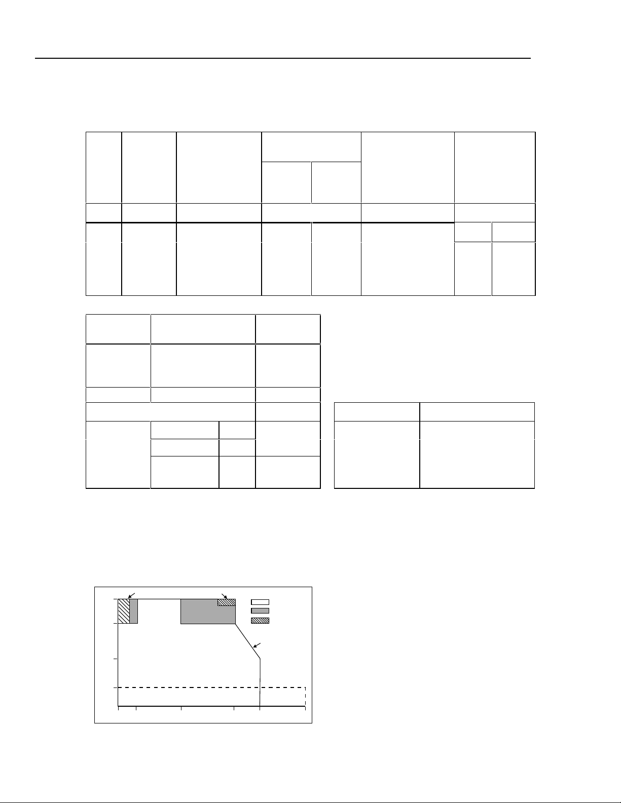
A diagram in the specifications tables at the end of this section illustrates the extended ac
volt-hertz product achieved by using a 5725A. Increased ac voltage load limits allow
using the 5700A Calibrator in systems with long cables.
Voltage output from the 5725A is available at the 5700A Calibrator front or rear binding
posts. This eliminates the need to move cables during a procedure that requires amplified
as well as standard calibrator outputs.
The 5725A front or rear panel OUTPUT binding posts are only for current output.
Extended-range ac and dc current is supplied through them. Since most meters with a
high current range use a separate high current input terminal, this configuration normally
eliminates the need to move cables during a procedure. If a single-point current output is
needed, the 5700A Calibrator can be configured to source all current outputs through the
5725A binding posts.
Enhancements to 5700A ac voltage output capability provided by the 5725A are as
follows:
1
• Frequency limits at higher voltage increase to 100 kHz at 750V, 30 kHz at 1100V.
• Load limits are to 70 mA for frequencies above 5 kHz, and to 50 mA for frequencies
less than 5 kHz.
• Capacitive load limits are increased to 1000 pF.
Model 5725A operating functions and ranges are as follows:
• AC voltage: 220 to 1100V rms up to 70 mA (50 mA < 5 kHz), 40 Hz to 30 kHz; 220
to 750V rms up to 70 mA, 30 kHz to 100 kHz
• DC current: 0 to ±11A
• AC current: 1 to 11A rms, 40 Hz to 10 kHz
1-3
Page 20

5725A
Instruction Manual
Where to Go From Here 1-2.
This manual is the operator and service manual for the 5725A. However, because the
5725A operates under the control of the 5700A Calibrator, most operating instructions
for the 5725A are in the 5700A manuals. Topics such as selecting output values,
connecting to a UUT (Unit Under Test), and self calibration are covered in the 5700A
Operator Manual. The list below gives some specific pointers, and the text further on
describes how to use all the manuals to find 5725A information.
For More Information About: Refer To:
• Unpacking and setup Section 2 of this manual
• Installation and rack mounting Section 2 of this manual and the
Y5735/Y5737 Instruction Sheet
• AC line power and interface cabling Section 2 of this manual
• Controls, indicators, and binding
Section 3 of this manual
posts
• 5725A service information Sections 4 through 9 of this manual
• Operating the amplifier Section 3 of this manual and Section 4 of
the 5700A Operator Manual
• Cabling to a Unit Under Test Section 4 of the 5700A Operator Manual
• Self calibration Section 7 of the 5700A Operator Manual
• Full verification Section 3 of the 5700A Service Manual
• IEEE-488 or serial remote operation Section 5 of the 5700A Operator Manual
• 5700A/5725A specifications Section 1 of this manual
• Theory of operation Section 4 and 9 of this manual
• Troubleshooting Section 6 of this manual
• Ordering a part Section 8 of this manual
1-4
Page 21

Introduction and Specifications
How to Use the Manuals
How to Use the Manuals 1-3.
The following paragraphs describe how each manual addresses the 5725A.
5725A Instruction Manual 1-4.
Use the 5725A Instruction Manual for installing the 5725A, learning about its front and
rear panel features, and for all service-related topics such as maintenance,
troubleshooting, parts lists, and schematics. (The 5725A Instruction Manual is the
service and operator manual for the 5725A.)
Although the instruction manual also contains a section devoted to 5725A operating
notes, once the 5725A is up and running you will find that the 5700A Operator Manual
contains most of the information you need to operate the 5725A.
5700A Operator Manual 1-5.
The 5700A Operator Manual contains the following information pertaining to the
5725A:
• Specifications for both the 5700A and 5725A (these same specifications are in this
Instruction Manual)
1
• Cable connections to a UUT for amplified voltage and current
• Front panel (local) operation
• Remote control operation, IEEE-488 or RS-232
• Self calibration
• Fault codes (these appear on the 5700A Control Display, or are read from the 5700A
in remote control operation)
• Calibration constant symbolic names
• Glossary of calibration-related terms
The 5700A Operator Manual comes with two pocket-sized booklets: one for front panel
operation and one for remote programming.
5700A Operator Reference Guide 1-6.
The 5700A Operator Reference Guide contains a summary of operating instructions
from the Operator Manual. This booklet contains information needed to start up and
operate the 5700A, but since the 5700A controls the 5725A, much of this information
applies to the 5725A. The booklet is included in the binder with the 5700A Operator
Manual.
5700A Remote Programming Reference Guide 1-7.
The 5700A Remote Programming Reference Guide contains a summary of remote
commands for the 5700A. It also contains information needed to determine system status
using the status byte and registers. Remote commands and system status apply to a
5725A under control of the 5700A. This booklet is also included in the binder with
5700A Operator Manual.
1-5
Page 22

5725A
Instruction Manual
5700A Service Manual 1-8.
Specifications 1-9.
The 5700A Service Manual is a maintenance guide for the 5700A. The following 5725A
topics are included in the 5700A Service Manual:
• Specifications for both the 5700A and 5725A (these same specifications are in this
Instruction Manual)
• Full verification of the 5700A and 5725A (recommended every two years)
• Calibration of the 5700A and 5725A (same procedure as in the 5700A Operator
Manual)
Specifications are valid after allowing a warm-up period of 30 minutes, or if the 5725A
has been recently on, twice the time the 5725A has been turned off. For example, if the
5725A has been turned off for five minutes, the warm-up period is ten minutes.
Absolute uncertainty includes stability, temperature coefficient, linearity, line and load
regulation, and traceability to external standards. You do not need to add anything to
absolute uncertainty to determine the ratios between 5700A/5725A uncertainties and the
uncertainties of your calibration workload.
Relative uncertainty specifications are provided for enhanced accuracy applications.
These specifications apply when range constants are adjusted (see "Range Calibration"
in the 5700A Operator Manual). To calculate absolute uncertainty, you must combine
the uncertainties of your external standards and techniques with relative uncertainty.
Secondary performance specifications and operating characteristics are included in the
uncertainty specifications. They are also provided separately for special calibration
requirements such as stability or linearity testing.
1-6
Page 23
DC Voltage
Introduction and Specifications
Specifications
1
Range Resolution
Absolute Uncertainty
± 5°C from calibration temperature
24 Hours 90 Days 180 Days 1 Year 24 Hours 90 Days
Relative Uncertainty
± 1°C
± (ppm output + µV) ± (ppm output + µV)
220 mV 10 nV 6.5 + .75 7 + .75 8 + .75 9 + .8 2.5 + .5 4 + .5
2.2V 100 nV 3.5 + 1.2 6 + 1.2 7 + 1.2 8 + 1.2 2.5 + 1.2 4 + 1.2
11V 1 µV 3.5 + 3 5 + 4 7 + 4 8 + 4 1.5 + 3 3.5 + 4
22V 1 µV 3.5 + 6 5 + 8 7 + 8 8 + 8 1.5 + 6 3.5 + 8
220V 10 µV 5 + 100 6 + 100 8 + 100 9 + 100 2.5 + 100 4 + 100
1100V 100 µV 7 + 600 8 + 600 10 + 600 11 + 600 3 + 600 4.5 + 600
Secondary Performance Specifications and Operating Characteristics
Included in Uncertainty Specifications
Range
Stability
± 1°C
24 Hours
Temperature Coefficient
[Note]
0°-10°C
10°-40°C
and
Linearity
± 1°C
Bandwidth
0.1-10 Hz
Noise
Bandwidth
10-10 kHz
40°-50°C pk-pk RMS
± (ppm output + µV) ± (ppm output + µV)/°C ± (ppm output + µV) µV
220 mV
2.2V
11V
22V
220V
1100V
Note: Temperature coefficient is an adder to uncertainty specifications that does not apply unless operating more than ±5°C from calibration
temperature.
.3 + .3
.3 + 1
.3 + 2.5
.4 + 5
.5 + 40
.5 + 200
.4 + .1
.3 + .1
.15 + .2
.2 + .4
.3 + 5
.5 + 10
1.5 + .5
1.5 + 2
1 + 1.5
1.5 + 3
1.5 + 40
3 + 200
1 + .2
1 + .6
.3 + 2
.3 + 4
1 + 40
1 + 200
.15 + .1
.15 + .4
.15 + 2
.15 + 4
.15 + 60
.15 + 300
5
15
50
50
150
500
Minimum output: 0V for all ranges, except 100V for 1100V range
Maximum load: 50 mA for 2.2V through 220V ranges; 20 mA for 1100V range; 50Ω output impedance on
220 mV range; all ranges <1000 pF,>25Ω
Load regulation: <0.2 ppm + 0.2 µV change, full load to no load
Line regulation: <0.1 ppm change, ±10% of selected nominal line
Settling time: 3 seconds to full accuracy; + 1 second for range or polarity change; + 1 second for 1100V
range
Overshoot: <5%
Common mode rejection: 140 dB, DC to 400 Hz
Remote sensing: Available 0V to ±1100V, on 2.2V through 1100V ranges
1-7
Page 24
5725A
Instruction Manual
AC Voltage
Range Resolution Frequency
2.2 mV 1 nV
22 mV 10 nV
220 mV 100 nV
2.2V 1 µV
22V 10 µV
220V 100 µV
1100V 11 mV 50-1k 75 + 4 80 + 4 85 + 4 90 + 4 50 + 4 55 + 4
5725A Amplifier:
1100V
750V
1 mV
Hz
10-20
20-40
40-20k
20k-50k
50k-100k
100k-300k
300k-500k
500k-1M
10-20
20-40
40-20k
20k-50k
50k-100k
100k-300k
300k-500k
500k-1M
10-20
20-40
40-20k
20k-50k
50k-100k
100k-300k
300k-500k
500k-1M
10-20
20-40
40-20k
20k-50k
50k-100k
100k-300k
300k-500k
500k-1M
10-20
20-40
40-20k
20k-50k
50k-100k
100k-300k
300k-500k
500k-1M
10-20
20-40
40-20k
20k-50k
50k-100k
100k-300k
300k-500k
500k-1M
40-1k
1k-20k
20k-30k
30k-50k
50k-100k
Absolute Uncertainty
5°C from calibration temperature
±
24 Hours 90 Days 180 Days 1 Year 24 Hours 90 Days
(ppm output + µV)
±
500 + 5
200 + 5
100 + 5
340 + 5
800 + 8
.11% + 15
.15% + 30
.4% + 40
500 + 6
200 + 6
100 + 6
340 + 6
800 + 8
.11% + 15
.15% + 30
.4% + 40
500 + 16
200 + 10
95 + 10
300 + 10
750 + 30
940 + 30
.15% + 40
.30% + 100
500 + 100
150 + 30
70 + 7
120 + 20
230 + 80
400 + 150
.10% + 400
.20% + 1 mV
500 + 1 mV
150 + 300
70 + 70
120 + 200
230 + 400
500 + 1.7 mV
.12% + 5 mV
.26% + 9 mV
(ppm output + mV)
±
500 + 10
150 + 3
75 + 1
200 + 4
500 + 10
.15% + 110
.50% + 110
1.20% + 220
75 + 4
105 + 6
230 + 11
230 + 11
600 + 45
550 + 5
220 + 5
110 + 5
370 + 5
900 + 8
.12% + 15
.17% + 30
.44% + 4
550 + 6
220 + 6
110 + 6
370 + 6
900 + 8
.12% + 15
.17% + 30
.44% + 4
550 + 16
220 + 10
100 + 10
330 + 10
800 + 30
.1% + 30
.17% + 40
.33% + 100
550 + 100
170 + 30
75 + 7
130 + 20
250 + 80
440 + 150
.11% + 400
.22% + 1 mV
550 + 1 mV
170 + 300
75 + 70
130 + 200
250 + 400
550 + 1.7 mV
.13% + 5 mV
.28% + 9 mV
550 + 10
170 + 3
80 + 1
220 + 4
550 + 10
.15% + 110
.52% + 110
1.25% + 220
80 + 4
125 + 6
360 + 11
360 + 11
.13% + 45
600 + 5
230 + 5
120 + 5
390 + 5
950 + 8
.13% + 15
.17% + 30
.47% + 40
600 + 6
230 + 6
120 + 6
390 + 6
950 + 8
.13% + 15
.17% + 30
.47% + 40
600 + 16
230 + 10
110 + 10
350 + 10
850 + 30
.11% + 30
.17% + 40
.35% + 100
600 + 100
170 + 30
80 + 7
140 + 20
270 + 80
470 + 150
.12% + 400
.23% + 1 mV
600 + 1 mV
170 + 300
80 + 70
140 + 200
270 + 400
550 + 1.7 mV
.13% + 5 mV
.29% + 9 mV
600 + 10
170 + 3
85 + 1
240 + 4
600 + 10
.16% + 110
.53% + 110
1.25% + 220
85 + 4
135 + 6
440 + 11
440 + 11
.16% + 45
600 + 5
240 + 5
120 + 5
410 + 5
950 + 8
.13% + 15
.18% + 30
.48% + 40
600 + 6
240 + 6
120 + 6
410 + 6
950 + 8
.13% + 15
.18% + 30
.48% + 40
600 + 16
240 + 10
110 + 10
360 + 10
900 + 30
.11% + 30
.18% + 40
.36% + 100
600 + 100
180 + 30
85 + 7
140 + 20
280 + 80
480 + 150
.12% + 400
.24% + 1 mV
600 + 1 mV
180 + 300
85 + 70
140 + 200
280 + 400
600 + 1.7 mV
.14% + 5 mV
.30% + 9 mV
600 + 10
180 + 3
90 + 1
250 + 4
600 + 10
.16% + 110
.54% + 110
1.30% + 220
90 + 4
165 + 6
600 + 11
600 + 11
.23% + 45
Relative Uncertainty
±
(ppm output + µV)
±
500 + 5
200 + 5
60 + 5
100 + 5
220 + 8
400 + 15
.10% + 30
.3% + 30
500 + 6
200 + 6
60 + 6
100 + 6
220 + 8
400 + 15
.10% + 30
.3% + 30
500 + 16
200 + 10
60 + 10
100 + 10
220 + 30
400 + 30
.1% + 40
.3% + 100
500 + 100
150 + 30
40 + 7
100 + 20
200 + 80
400 + 150
.1% + 400
.2% + 1 mV
500 + 1 mV
150 + 300
40 + 70
100 + 200
200 + 400
500 + 1.7 mV
.12% + 5 mV
.26% + 9 mV
(ppm output + mV)
±
500 + 10
150 + 3
45 + 1
100 + 1
300 + 10
.15% + 110
.50% + 110
1.20% + 220
50 + 4
85 + 6
160 + 11
160 + 11
380 + 45
1°C
550 + 5
220 + 5
65 + 5
110 + 5
240 + 8
440 + 15
.11% + 30
.33% + 30
550 + 6
220 + 6
65 + 6
110 + 6
240 + 8
440 + 15
.11% + 30
.33% + 30
550 + 16
220 + 10
65 + 10
110 + 10
240 + 30
440 + 30
.11% + 40
.33% + 100
550 + 100
170 + 30
45 + 7
110 + 20
220 + 80
440 + 150
.11% + 400
.22% + 1 mV
550 + 1 mV
170 + 300
45 + 70
110 + 200
220 + 400
550 + 1.7 mV
.13% + 5 mV
.28% + 9 mV
550 + 10
170 + 3
50 + 1
110 + 1
330 + 10
.15% + 100
.52% + 110
1.20% + 220
55 + 4
105 + 6
320 + 11
320 + 11
.12% + 45
1-8
Page 25
Introduction and Specifications
AC Voltage (continued)
Secondary Performance Specifications and Operating Characteristics
Included in Uncertainty Specifications
Stability
Range Frequency ± 1°C
Hz ± µV ±µV/°C Ω± (% output + µV)
10-20
20-40
40-20k
2.2 mV
22 mV
220 mV
2.2V
22V
220V
1100V 50-1k 20 + .5 2 5 10 + 1 .07
20k-50k
50k-100k
100k-300k
300k-500k
500k-1M
10-20
20-40
40-20k
20k-50k
50k-100k
100k-300k
300k-500k
500k-1M
10-20
20-40
40-20k
20k-50k
50k-100k
100k-300k
300k-500k
500k-1M
10-20
20-40
40-20k
20k-50k
50k-100k
100k-300k
300k-500k
500k-1M
10-20
20-40
40-20k
20k-50k
50k-100k
100k-300k
300k-500k
500k-1M
10-20
20-40
40-20k
20k-50k
50k-100k
100k-300k
300k-500k
500k-1M
24 Hours
5
5
2
2
3
3
5
5
5
5
2
2
3
5
10
15
± (ppm output + µV) ± (ppm output µV)/°C
150 + 20
80 + 15
12 + 2
10 + 2
10 + 2
20 + 4
100 + 10
200 + 20
150 + 20
80 + 15
12 + 4
15 + 5
15 + 5
30 + 10
70 + 20
150 + 50
150 + 20
80 + 15
12 + 8
15 + 10
15 + 10
30 + 15
70 + 100
150 + 100
150 + 200
80 + 150
12 + 80
15 + 100
15 + 100
30 + 400
100 + 10 mV
200 + 20 mV
±(ppm output + mV) ±(ppm output)/°C ±(% output)
Temperature
Coefficient
10°-40°C
.05
.05
.05
.1
.2
.3
.4
.5
.2
.2
.2
.4
.5
.6
1
1
2 + 1
2 + 1
2 + 1
15 + 2
15 + 4
80 + 5
80 + 5
80 + 5
50 + 10
15 + 5
2 + 1
10 + 2
10 + 4
80 + 15
80 + 40
80 + 100
50 + 100
15 + 30
2 + 10
10 + 20
10 + 40
80 + 150
80 + 300
80 + 500
50 + 1 mV
15 +300
2 + 80
10 + 100
10 + 500
80 + 600
80 + 800
80 + 1 mV
0°-10°C
and
40°-50°C
.05
.05
.05
.1
.2
.3
.4
.5
.3
.3
.3
.5
.5
.6
1
1
2 + 1
2 + 1
2 + 1
15 + 2
15 + 4
80 + 5
80 + 5
80 + 5
50 + 10
15 + 5
5 + 2
15 + 4
20 + 4
80 + 15
80 + 40
80 + 100
50 + 100
15 + 40
4 + 15
20 + 20
20 + 40
80 + 150
80 + 300
80 + 500
50 + 1 mV
15 + 300
4 + 80
20 + 100
20 + 500
80 + 600
80 + 800
80 + 1 mV
Output Impedance Bandwidt h
50
50
50
Load Regulation
± (ppm output + µV)
10 + 2
10 + 2
10 + 4
30 + 10
120 + 16
300 ppm
600 ppm
.12%
10 + 20
10 + 20
10 + 30
30 + 50
80 + 80
100 + 700
200 + 1.1 mV
600 + 3.0 mV
10 + .2 mV
10 + .2 mV
10 + .3 mV
30 + .6 mV
80 + 3 mV
250 + 25 mV
500 + 50 mV
1000 + 110 mV
Maximum
Distortion
10 Hz-10 MHz
.05 + 10
.035 + 10
.035 + 10
.035 + 10
.035 + 10
.3 + 30
.3 + 30
2 + 30
.05 + 11
.035 + 11
.035 + 11
.035 + 11
.035 + 11
.3 + 30
.3 + 30
1 + 30
.05 + 16
.035 + 16
.035 + 16
.035 + 16
.035 + 16
.3 + 30
.3 + 30
2 + 30
.05 + 80
.035 + 80
.035 + 80
.035 + 80
.035 + 80
.3 + 110
.3 + 110
1 + 110
.05 + 700
.035 + 700
.035 + 700
.035 + 700
.035 + 700
.3 + 800
.3 + 800
2 + 800
.05 + 10 mV
.05 + 10 mV
.05 + 10 mV
.05 + 10 mV
.1 + 13 mV
1.5 + 50 mV
1.5 + 50 mV
3.5 + 100 mV
Specifications
1
1-9
Page 26
5725A
Instruction Manual
AC Voltage (continued)
Secondary Performance and Operating Characteristics (continued)
Included in Uncertainty Specifications
5725A Amplifier:
Stability
Temperature Coefficient
Range Frequency ±1°C
24 Hours
10°-40°C
Hz ±(ppm output + mV) ±(ppm output)/°C ±(ppm output + m V )
1100V
1k-20k
20k-50k
50k-100k
40-1k
Voltage
Maximum Current
Range
2.2V [Note 1]
22V
220V
1100V 6 mA 600 pF
5725A Amplifier: 1000 pF [Note 2]
1100V 5 kHz-30 kHz 70 mA
Notes:
1. 2.2V Range, 100 kHz-1.2 MHz only: uncertainty specifications cover
loads to 10 mA or 1000 pF. For higher loads, load regulation is
added.
2. The 5725A will drive up to 1000 pF of load capacitance. Uncertainty
specifications include loads to 300 pF and 150 pF as shown under
"Load Limits." For capacitance’s up to the maximum of 1000 pF, add
"Load Regulation."
3. Applies from 0°C to 40°C
100V
220V
22V
VOLTAGE
3.5V
40 Hz 30 kHz
VOLT-HERTZ CAPABILITY
10 Hz 50 Hz 1 kHz 100 kHz 1 MHz
50 mA, 0°C-40°C
20 mA, 40°C-50°C
40 Hz-5 kHz 50 mA <20 7
30 kHz-100 kHz 70 mA
10 + .5
15 + 2
40 + 2
130 + 2
Limits
FREQUENCY
[Note 3]
5
5
10
30
Load Limits
>50Ω,
1000 pF
300 pF 120-120k 5
150 pF
5700A
5725A
5205A or
5215A
7
2.2 x 10
V-Hz
5700A-03
30 MHz
Load Regulation Distortion
0°-10°C
and
[Note 2] Bandwidth
10 Hz-10 MHz
40°-50°C
±(% output)
150 pF 1000 pF
5
5
10
30
Output display formats: Voltage or dBm, dBm reference
600Ω.
Minimum output: 10% on each range
External sense: Selectable for 2.2v, 22V, 220V, and
1100V ranges; 5700A <100 kHz, 5725A <30 kHz
Settling time to full accuracy:
10 + 1
90 + 6
275 + 11
500 + 30
.10
.10
.30
.40
Frequency (Hz) Settling time (seconds)
>120k 2
+ 1 second for amplitude or frequency range change; + 2
seconds for 5700A 1100V range; + 4 seconds for 5725A
1100V range
Overshoot: <10%
Common mode rejection: 140 dB, DC to 400 Hz
Frequency:
Ranges (Hz):
10.000-11.999, 12.00-119.99
120.0-1199.9, 1.200k-11.999k
12.00k-119.99k, 120.0k-1.1999
Uncertainty: ±0.01%
Resolution: 11.999 counts
Phase lock: Selectable rear panel BNC input
Phase uncertainty (except 1100V range):
>30 Hz: ±1° + 0.05°/kHz), <30 Hz: ±3
Input voltage: 1V to 10V rms sine wave (do not exceed 1V for
mV ranges)
Frequency range: 10 Hz to 1.1999 MHz
Lock range: ±2% of frequency
Lock-in time: Larger of 10/frequency or 10 msec
Phase reference: Selectable, rear panel BNC output
Range: ±180
Phase Uncertainty (except 1100V range):
±1°
Stability: ±0.1°
Resolution: 1°
Output level: 2.5V rms ±0.2V
Frequency range: 50 kHz to 1 kHz, useable 10 Hz to 1.1999
MHz
°
at quadrature points (0°, ±90°, ±180°) elsewhere ±2
°
.10
.15
.30
.40
°
1-10
Page 27
Introduction and Specifications
Specifications
Resistance
Nominal
Value
Ω ±ppm ±ppm
0
1
1.9
10
19
100
190
1k
1.9k
10k
19k
100k
190k
1M
1.9M
10M
19M
100M
±5°C from calibration temperature [Note 1]
24 Hours 90 Days 180 Days 1 Year 24 Hours 90 Days
50
µΩ
85
85
26
24
15
15
11
11
9
9
11
11
16
17
33
43
110
50
µΩ
95
95
28
26
17
17
12
12
11
11
13
13
18
19
37
47
120
50
µΩ
100
100
30
28
18
18
13
13
12
12
14
14
20
21
40
50
125
50
µΩ
110
110
33
31
20
20
15
15
14
14
16
16
23
24
46
55
130
Secondary Performance Specifications and Operating Characteristics
Included in Uncertainty Specifications
Absolute Uncertainty of Characterized Value
Nominal Stability
Value
±1°C
24 Hours
Temperature
Coefficient
[Note 2]
10°-40°C
0°-10°C
and
Full
Spec
Load
Range
[Note 3]
Maximum
Peak
Current
40°-50°C Value
Ω±ppm ±ppm/°C mA mA ±ppm ±mΩ
0
13245
1.9 25 6 7
10 5 2 3
19 4 2 3
100 2 2 3
190 2 2 3
1k 2 2 3
1.9k 2 2 3
10k 2 2 3
19k 2 2 3
100k 2 2 3
190k 2 2 3
1M 2.5 2.5 6
1.9M 3.5 3 10
10M 10 5 20
19M 20 8 40
100M 50 12 100
Notes:
1. Specifications apply to displayed value. 4-wire connections, except 100 mΩ.
2. Temperature coefficient is an adder to uncertainty specifications that does not apply unless operated more than 5°C from calibration
temperature, or calibrated outside the range 19°C to 24°C. Two examples:
a) Calibrate at 20°C: Temperature coefficient adder is not required unless operated below 15°C or above 25°C.
b) Calibrate at 26°C: Add 2°C temperature coefficient adder. Additional temperature coefficient adder is not required unless operated below
21°C or above 31°C.
3. Refer to current derating factors table for loads outside of this range.
4. Active two-wire compensation may be selected for values less than 100 kΩ, with either the front panel
reference plane. Active compensation is limited to 11 mA load, and to 2V burden. Two wire compensation can be used only with Ω meters that
source continuous (not pulsed) dc current.
8-500 500
8-100 700 500 2 4
8-100 500 500 2 4
8-11 220 300 2 4
8-11 160 300 2 4
8-11 70 150 2 4
8-11 50 150 2 4
1-2 22 150 10 15
1-1.5 16 150 10 15
100-500 µA 7 150 50 60
50-250 µA 5 150 100 120
10-100 µA 1 150
5-50 µA 500 µA 150
5-20 µA 100 µA 200
2.5-10 µA50
.5-2 µA10
.25-1 µA5
50-200 nA 1 µA 500
A 200
µ
A 300
µ
A 300
µ
Relative Uncertainty
50
µΩ
32
25
5
4
2
2
2
2
2
2
2
2
2.5
3.5
10
20
50
Maximum
Difference
of
Characterized
to Nominal
or the meter input terminals
±1°C
50
µΩ
40
33
8
7
4
4
3.5
3.5
3.5
3.5
3.5
3.5
5
6
14
24
60
Two-Wire Adder
active
compensation
[Note 4]
Lead
Resistance
0.1Ω 1Ω
24
as
1
1-11
Page 28
5725A
Instruction Manual
Current Derating Factors
Nominal Value Value of Derating Factor K for Over or Under Current
Ω
I<I
L
(Note 1)
Two-Wire Comp
Four-Wire
I<I
L
(Note 1)
Four-Wire
I
<I<I
U
(Note 2)
MAX
SHORT
1
1.9
10
19
100
190
1k
1.9k
10k
19k
100k
190k
1M
1.9M
10M
19M
100M
4.4
4.4
4.4
4.4
4.4
4.4
4.4
4.4
4.4
5000
5000
0.3
300
160
30
16
3.5
2.5
0.4
0.4
50
50
7.5
4.0
1.0
0.53
0.2
0.53
0.1
4 X 10
1.5 X 10
1.6 X 10
3 X 10
1 X 10
1.9 X 10
0.1
0.19
2.0
3.8
2 X 10
3.8 X 10
1.5 X 10
2.9 X 10
1 X 10
1.9 X 10
-5
-4
-3
-3
-2
-2
-5
-5
-4
-4
-3
-3
Notes:
, errors occur due to thermally generated voltages within the 5700A. Use the following equation to determine the error, and add
1. For I<I
L
this error to the corresponding UNCERTAINTY or STABILITY specification.
Error = K(I
- I)/(IL X I)
L
Where: Error is in mΩ for all TWO-WIRE COMP values and FOUR-WIRE SHORT, and in ppm for the remaining FOUR-WIRE values.
1-12
K is the constant from the above table;
are expressed in mA for SHORT to 1.9 kΩ;
I and I
L
are expressed in µA for 10 kΩ to 100 M
2. For I
I and I
L
<I<I
errors occur due to self-heating of the resistors in the 5700A. Use the following equation to determine the error in ppm and
U
MAX
Ω
add this error to the corresponding UNCERTAINTY or STABILITY specification.
2
2
-I
Error in ppm = K(I
)
U
Where: K is the constant from the above table;
are expressed in mA for SHORT to 19 kΩ;
I and I
U
are expressed in µA for 100 kΩ to 100 M
I and I
U
Ω
Page 29
DC Current
Range
Introduction and Specifications
Absolute Uncertainty
±5°C from calibration temperature
Resolution
For fields strengths >1 V/m but <3 V/m, add 1% of
range
24 Hours 90 Days 180 Days 1 Year 24 Hours 90 Days
nA ± (ppm output + nA) ± (ppm output + nA)
Relative Uncertainty ±1°C
Specifications
1
220 µA
2.2 mA
22 mA
.1
1
10
45 + 10
45 + 10
45 + 100
50 + 10
50 + 10
50 + 100
55 + 10
55 + 10
55 + 100
60 + 10
60 + 10
60 + 100
24 + 2
24 + 5
24 + 50
26 + 2
26 + 5
26 + 50
µA ± (ppm output + µA) ± (ppm output + µA)
220 mA
2.2A
[Note 1]
5725A Amplifier:
11A 10 330 + 470 340 + 480 350 + 480 360 + 480 100 + 130 110 + 130
Secondary Performance Specifications and Operating Characteristics
Included in Uncertainty Specifications
Range Stability ±1°C 24
V ± (ppm output + nA) ± (ppm output + nA)/°C ±nA/V Ω ppm output + nA nA
220 µA
2.2 mA
22 mA
220 mA
2.2A
5725A: ± (ppm output + µA) ± (ppm output + µA)/°C ppm output + µA µA
11A 25 + 100 20 + 75 30 + 120 4 0 4 15 + 70 175
Notes:
Maximum output from 5700A terminals is 2.2A. Uncertainty specifications for 220 µA and 2.2 mA ranges are increased by 1.3 X when
supplied through 5725A terminals.
Specifications are otherwise identical for all output locations.
1. Add to uncertainty specifications:
±200 X I
±10 X I
2. Temperature coefficient is an adder to uncertainty specifications. It does not apply unless operating more than ±5°C from calibration
temperature.
3. Burden voltage adder is an adder to uncertainty specifications that does not apply unless burden voltage is greater than 0.5V.
4. For higher loads, multiply uncertainty specification by:
5. 5700A compliance limit is 2V for outputs from 1A to 2.2A. 5725A Amplifier may be used in range-lock mode down to 0A.
Minimum output: 0 for all ranges, including 5725A.
Settling time to full accuracy: 1 second for µA and mA ranges; 3 seconds for 2.2A range; 6 seconds for 11A range; + 1 second for range
or polarity change
Overshoot: <5%
.1
1
Hours
5 + 1
5 + 5
5 + 50
8 + 300
9 + 7 µA
2
ppm for >100 mA on 220 mA range
2
ppm for >1A on 2.2A range
1 +
maximum load for full accuracy
55 + 1
75 + 30
Temperature Coefficient
10°-40°C
1 + .40
1 + 2
1 + 20
1 + 200
1 + 2.5 µΑ
0.1 x actual load
60 + 1
80 + 30
[Note 2]
0°-10°C
and
40°-50°C [Note 4] pk-pk RMS
3 + 1
3 + 10
3 + 100
3 + 1 µA
A3 + 10 µA
65 + 1
90 + 30
Compliance
Limits
10
10
10
10
3
[Note 5]
70 + 1
95 + 30
Burden
Voltage
Adder
[Note 3]
.2
.2
10
100
2 µA
Maximum
Load
For Full
Accuracy
20k
2k
200
20
2
26 + .3
40 + 7
Bandwidth
0.1-10 Hz
6 + .9
6 + 5
6 + 50
9 + 300
12 + 1.5 µA
30 + .3
45 + 7
Noise
Bandwidth
10-10 kHz
500
20 µA
10
10
50
1-13
Page 30
5725A
Instruction Manual
AC Current
Range Resolution
220 µA1 nA
2.2 mA 10 nA
22 mA 100 nA
220 mA 1 µA
2.2A 10 µA
5725A Amplifier:
11A 100 µA
Frequency
Hz
10-20
20-40
40-1k
1k-5k
5k-10k
10-20
20-40
40-1k
1k-5k
5k-10k
10-20
20-40
40-1k
1k-5k
5k-10k
Hz
10-20
20-40
40-1k
1k-5k
5k-10k
20-1k
1k-5k
5k-10k
40-1k
1k-5k
5k-10k
Absolute Uncertainty
5°C from calibration temperature
±
For fields strengths >1 V/m but <3 V/m, add 1% of range
24 Hours 90 Days 180 Days 1 Year 24 Hours 90 Days
(ppm output + nA)
±
650 + 30
350 + 25
120 + 20
500 + 50
.15% + 100
650 + 50
350 + 40
120 + 40
500 + 500
.15% + 1 µA
650 + 500
350 + 400
120 + 400
500 + 5 µA
.15% + 10 µA
650 + 5
350 + 4
120 + 4
500 + 50
.15% + 100
600 + 40
700 + 100
.80% + 200
370 + 170
800 + 380
.3% + 750
700 + 30
380 + 25
140 + 20
600 + 50
.16% + 100
700 + 50
380 + 40
140 + 40
600 + 500
.16% + 1 µA
700 + 500
380 + 400
140 + 400
600 + 5 µA
.16% + 10 µA
(ppm output + µA)
±
700 + 5
380 + 4
150 + 4
600 + 50
.16% + 100
650 + 40
750 + 100
.90% + 200
400 + 170
850 + 380
.33% + 750
750 + 30
410 + 25
150 + 20
650 + 50
.17% + 100
750 + 50
410 + 40
150 + 40
650 + 500
.17% + 1 µA
750 + 500
410 + 400
150 + 400
650 + 5 µA
.17% + 10 µA
750 + 5
410 + 4
170 + 4
650 + 50
.17% + 100
700 + 40
800 + 100
.95% + 200
440 + 170
900 + 380
.35% + 750
800 + 30
420 + 25
160 + 20
700 + 50
.18% + 100
800 + 50
420 + 40
160 + 40
700 + 500
.18% + 1 µA
800 + 500
420 + 400
160 + 400
700 + 5 µA
.18% + 10 µA
800 + 5
420 + 4
180 + 4
700 + 50
.18% + 100
750 + 40
850 + 100
1.0% + 200
460 + 170
950 + 380
.36% + 750
Relative Uncertainty
(ppm output + nA)
±
450 + 30
270 + 25
110 + 20
450 + 50
.14% + 100
450 + 50
270 + 40
110 + 40
450 + 500
.14% + 1 µA
450 + 500
270 + 400
110 + 400
450 + 5 µA
.14% + 10 µA
(ppm output + µA)
±
450 + 5
280 + 4
110 + 4
450 + 50
.14% + 100
600 + 40
650 + 100
.75% + 200
300 + 170
700 + 380
.28% + 750
1°C
±
.15% + 100
.15% + 1 µA
500 + 5 µA
.15% + 10 µA
.15% + 100
.85% + 200
.32% + 750
500 + 30
300 + 25
120 + 20
500 + 50
500 + 50
300 + 40
120 + 40
500 + 500
500 + 500
300 + 400
120 + 400
500 + 5
300 + 4
130 + 4
500 + 50
650 + 40
750 + 100
330 + 170
800 + 380
1-14
Page 31

Introduction and Specifications
Specifications
AC Current (continued)
Secondary Performance Specifications and Operating Characteristics
Included in Uncertainty Specifications
Stability
Range Frequency
Hz ± (ppm output + nA) ± (ppm output + nA)/°C V rms Ω± (% output + µA)
10-20
220 µA
2.2 mA
22 mA
220 mA
2.2A
5725A Amplifier: ± (% output)
11A
Notes:
Maximum output from 5700A terminals is 2.2A. Uncertainty specifications for 220 µA and 2.2 mA ranges are increased by 1.3 x plus 2 µA when
supplied through 5725A terminals. Specifications are otherwise identical for all output locations.
1. Temperature coefficient is an adder to uncertainty specifications that does not apply unless operating more than ±5°C from calibration temperature.
2. For larger resistive loads multiply uncertainty specifications by:
(
maximum load for full acuracy
3. 1.5V compliance limit above 1A. 5725A Amplifier may be used in range-lock mode down to 1A.
4. For resistive loads within rated compliance voltage limits.
Minimum output:: 9 µA for 220 µA range, 10% on all other ranges. 1A minimum for 5725A.
Inductive load limits: 400 µH (5700A or 5725A). 20 µH for 5700A output >1A.
Power factors: 5700A, 0.9 to 1; 5725A, 0.1 to 1. Subject to compliance voltage limits.
Frequency:
Range (Hz):
10.000-11.999, 12.00-119.99,
120.0-1199.9, 1.200k-10.000k
Uncertainty: ±0.01%
Resolution: 11,999 counts
Settling time to full accuracy: 5 seconds for 5700A ranges; 6 seconds for 5725A 11A range; +1 second for amplitude or frequency range change.
Overshoot: <10%
20-40
40-1k
1k-5k
5k-10k
10-20
20-40
40-1k
1k-5k
5k-10k
10-20
20-40
40-1k
1k-5k
5k-10k
Hz ± (ppm output + µA) ± (ppm output + µA)/°C
10-20
20-40
40-1k
1k-5k
5k-10k
20-1k
1k-5k
5k-10k
40-1k
1k-5k
5k-10k
actual load
±1°C
24 Hours
150 + 5
80 + 5
30 + 3
50 + 20
400 + 100
150 + 5
80 + 5
30 + 3
50 + 20
400 + 100
150 + 50
80 + 50
30 + 30
50 + 500
400 + 1 µA
150 + .5
80 + .5
30 + .3
50 + 3
400 + 5
50 + 5
80 + 20
800 + 50
75 + 100
100 + 150
200 + 300
2
)
Temperature Coefficient
[Note 1]
0°-10°C
10°-40°C
50 + 5
20 + 5
4 + .5
10 + 1
20 + 100
50 + 5
20 + 4
4 + 1
10 + 100
50 + 400
50 + 10
20 + 10
4 + 10
10 + 500
50 + 1 µA
50 + .05
20 + .05
4 + .1
10 + 2
50 + 5
4 + 1
10 + 5
50 + 10
20 + 75
40 + 75
100 + 75
and
40°-50°C
50 + 5
20 + 5
10 + .5
20 + 1
20 + 100
50 + 5
20 + 4
10 + 2
20 + 100
50 + 400
50 + 10
20 + 10
10 + 20
20 + 400
50 + 1 µA
50 + .05
20 + .05
10 + .1
20 + 2
50 + 5
10 + 1
20 + 5
50 + 10
30 + 75
50 + 75
100 + 75
Compliance
Limits For Full
72k
7 500
7 150
715
1.4
[Note 3]
33
Maximum
Resistive
Load
Accuracy
[Note 2]
.5
Noise and
Distortion
Bandwidth
10 Hz-50 kHz
<0.5V Burden
.05 + .1
.05 + .1
.05 + .1
.25 + .5
.5 + 1
.05 + .1
.05 + .1
.05 + .1
.25 + .5
.5 + 1
.05 + .1
.05 + .1
.05 + .1
.25 + .5
.5 + 1
.05 + 10
.05 + 10
.05 + 10
.25 + 50
.5 + 100
.5 + 100
.3 + 500
1 + 1 mA
.
05
[Note 4]
.
12
.
5
1
1-15
Page 32

5725A
Instruction Manual
Wideband AC Voltage (Option -03)
Specifications apply to the end of the cable and 50Ω termination used for calibration:
Range
±5°C from calibration temperature
30 Hz-500 kHz
Absolute Uncertainty
Volts dBm
Resolution
24 Hours 90 Days 180 Days 1 Year
± (% output + µV)
1.1 mV -46 10 nV .4 + .4 .5 + .4 .6 + .4 .8 + 2
3 mV -37 10 nV .4 + 1 .45 + 1 .5 + 1 .7 + 3
11 mV -26 100 nV .2 + 4 .35 + 4 .5 + 4 .7 + 8
33 mV -17 100 nV .2 + 10 .3 + 10 .45 + 10 .6 + 16
110 mV -6.2 1 µV .2 + 40 .3 + 40 .45 + 40 .6 + 40
330 mV +3.4 1 µV 0.2 + 100 0.25 + 100 .35 + 100 .5 + 100
1.1V +14 10 µV .2 + 400 .25 + 400 .35 + 400 .5 + 400
3.5V +24 10 µV 15 + 500 .2 + 500 .3 + 500 .4 + 500
Settling
Time To
Full
Accuracy
Harmonic
Distortion
Frequency
Frequency
Resolution
Amplitude Flatness, 1 kHz
Reference
Voltage Range
Temperature
Coefficient
1.1 mV 3 mV >3 mV
Hz Hz ±% ±ppm/°C Seconds dB
10-30 .01 .3 .3 .3 100 7 -40
30-120 .01 .1 .1 .1 100 7 -40
120-1.2k .1 .1 .1 .1 100 5 -40
1.2k-12k 1 .1 .1 .1 100 5 -40
12k-120k 10 .1 .1 .1 100 5 -40
120k-1.2M 100 .2 + 3 µV.1 + 3 µV.1 + 3 µV 100 5 -40
1.2M-2M 100k .2 + 3 µV.1 + 3 µV.1 + 3 µV 100 0.5 -40
2M-10M 100k .4 + 3 µV.3 + 3 µV.2 + 3 µV 100 0.5 -40
10M-20M 1M .6 + 3 µV.5 + 3 µV.4 + 3 µV 150 0.5 -34
20M-30M 1M 1.5 + 15 µV 1.5 + 3 µV1 + 3 µV 300 0.5 -34
1-16
Additional Operating Information:
dBm reference = 50Ω
Range boundaries are at voltage points, dBm levels are approximate .
Power
dBm = 10 log (
0.22361V across 50Ω = 1 mW or 0 dBm
Minimum output: 300 µV (-57 dBm)
Frequency uncertainty: ±0.01%
Frequency resolution: 11,999 counts to 1.1999 MHz, 119 counts to 30 MHz.
Overload protection: A short circuit on the wideband output will not result in damage. After settling time,
),
1 mW
normal operation is restored upon removal.
Page 33

Introduction and Specifications
Specifications
General Specifications:
Warm-Up time: 2 X the time since last warmed up, to a maximum of 30 minutes.
System installation: Rear output configuration and rack- mount kit available.
Standard interfaces: IEEE-488, RS-232, 5725A, 5205A or 5215A, 5220A, phase lock in (BNC), phase
reference out (BNC).
Temperature performance: Operating: 0°C to 50°C.
Calibration: 15°C to 35°C. Storage: -40°C to 75°C.
Relative humidity: Operating: <80% to 30°C, <70% to 40°C, <40% to 50°C.
Storage: <95%, non-condensing.
Safety: Designed to comply with UL1244 (1987); IEC 348-1978; IEC 66E (CO) 4; CSA 556B.
Guard isolation: 20 volts
EMI/RFI: Designed to comply with FCC Rules Part 15, Subpart J, Class B; VDE 0871, Class B.
Reliability: MIL-T-28800D, para. 3.13.3.
Line Power: 47 to 63 Hz; ±10% allowed about selectable nominal line voltage: 100V, 110V, 115V, 120V,
200V, 220V, 230V, 240V. Maximum power: 5700A, 300 VA; 5725A, 750 VA.
1
Electromagnetic Compatibility: This instrument is designed to operate in Standards Laboratory
environments where in electromagnetic is highly controlled. If used in areas with RF fields >0.78 V/m there
could be errors in measurements.
Size:
5700A: Height 17.8 cm (7 in), standard rack increment, plus 1.5 cm (0.6 in) for feet; Width 43.2 cm (17 in),
standard rack width; Depth 63.0 cm (24.8 in), overall; 57.8 cm (22.7 in), rack depth.
5725A: Height 13.3 cm, (5.25 in); Width and depth same as 5700A. Both units project 5.1 cm, (2 in) from
rack front.
Weight: 5700A: 27 kg (62 lbs); 5725A: 32 kg (70 lbs).
43.2 cm (17 in)
17.8 cm (7 in)
63 cm (24.8 in)
6.35 cm (2.5 in)
FOR CABLE
ACCESS
1-17
Page 34

5725A
Instruction Manual
1-18
Page 35

Chapter 2
Installation
Title Page
2-1. Introduction.......................................................................................... 2-3
2-2. Unpacking and Inspection.................................................................... 2-3
2-3. Service Information.............................................................................. 2-5
2-4. Placement and Rack Mounting............................................................. 2-5
2-5. Cooling Considerations........................................................................ 2-5
2-6. Connecting to the 5700A Calibrator .................................................... 2-6
2-7. Selecting Line Voltage......................................................................... 2-7
2-8. Accessing the Fuse............................................................................... 2-8
2-9. Connecting to Line Power.................................................................... 2-9
2-1
Page 36

5725A
Instruction Manual
2-2
Page 37

Installation
Introduction
Warning
The 5725A amplifier is capable of supplyi ng l et hal voltages. Do
not touch the 5700A output terminals. Read t hi s section before
operating the 5725A.
Introduction 2-1.
This section provides instructions for unpacking and installing the 5725A. Procedures
for line voltage selection, fuse replacement, and connection to line power and the 5700A
Calibrator are provided here. Read this section before operating the 5725A.
Instructions for connecting cables to a UUT (Unit Under Test) are in Section 4 of the
5700A Operator Manual.
Unpacking and Inspection 2-2.
The 5725A is shipped in a container that is specially designed to prevent damage during
shipping. Inspect the 5725A carefully for damage, and immediately report any damage
to the shipper. Instructions for inspection and claims are included in the shipping
container.
2
If you need to reship the 5725A, use the original container. If it is not available, you can
order a new container from Fluke by identifying the amplifier’s model and serial number.
When you unpack the 5725A, check for all the standard equipment listed in Table 2-1.
Report any shortage to the place of purchase or to the nearest Technical Service Center.
(A List of Technical Service Centers is located in Section 8 of this manual.) If
performance tests are required for your acceptance procedures, refer to Section 3 of the
5700A Service Manual for instructions.
Line power cords available from Fluke are listed in Table 2-2 and illustrated in
Figure 2-1.
Table 2-1. Standard Equipment
Item Model or Part Number
Amplifier 5725A
Line Power Cord (See Table 2-2 and Figure 2-1)
Shielded 5700A/5725A Interface Cable 842901
5725A Instruction Manual 823435
Spare 4A, 250V Fuse 216846
Certificate of Calibration (None)
2-3
Page 38

5725A
Instruction Manual
Table 2-2. Line Power Cord Types Available from Fluke
TYPE VOLTAGE/CURRENT FLUKE OPTION NUMBER
North America 120V/15A LC-1
North America 240V/15A LC-2
Universal Euro 220V/16A LC-3
United Kingdom 240V/13A LC-4
Switzerland 220V/10A LC-5
Australia 240V/10A LC-6
South Africa 240V/5A LC-7
LC-1 LC-2 LC-3 LC-4
LC-5 LC-6 LC-7
Figure 2-1. Line Power Cords Available for Fluke Instruments
aq2f.eps
2-4
Page 39

Installation
Service Information
Service Information 2-3.
Each 5725A Amplifier is warranted to the original purchaser for a period of one year
beginning on the date received. The warranty is located at the front of this manual.
Factory-authorized service and technical advice for the 5725A is available at Fluke
Service Centers. Section 8 contains a list of Service Centers.
Warning
Servicing described in this manual is t o be done by qual i fied
service personnel only. To avoid electrical shock, do not
service the 5725A unless you are qualified to do so.
The owner may choose to repair a 5725A using the troubleshooting information in
Section 7 to isolate a faulty module, then use the Module Exchange Program. Refer to
the Fluke catalog or contact a Service Center representative for the module exchange
procedure.
Placement and Rack Mounting 2-4.
You can stack the 5725A on top of or below the 5700A Calibrator. (Choose the
configuration that provides the easiest access to the 5700A Calibrator controls.) Or, you
can mount the 5725A in a standard-width, 24-inch (61-cm) deep equipment rack. For
bench-top stacking, the 5725A is equipped with non-skid feet. To mount the 5725A in an
equipment rack, order the accessory 5725A Rack Mount Kit, Model Y5735. An
instruction sheet is packed with the kit.
2
Caution
Use only the rack mount slides included in the Y5735 kit. Rack
mount slides intended for other instrument s can block the side
ventilation holes on the 5725A and cause overheating.
Cooling Considerations 2-5.
Caution
Damage caused by overheating may occur if the area around
the air intake is restricted, the int ake ai r i s t oo w arm, or t he f an
filter becomes clogged.
Accuracy and dependability of all internal parts of the 5725A are enhanced by
maintaining the coolest possible internal temperature. By observing the following rules
you can lengthen the life of the 5725A:
• The area around the fan filter must be at least 3 inches from nearby walls or rack
enclosures.
• Exhaust perforations on the sides of the 5725A must be clear of obstructions. Most
of the heat exits from the side vents near the front.
• Air entering the instrument must be room temperature. Make sure that exhaust from
another instrument is not directed into the fan inlet.
• Clean the fan filter every 30 days, or more frequently if the 5725A is operated in a
dusty environment. (Instructions for cleaning the fan filter are in Section 6.)
2-5
Page 40

5725A
Instruction Manual
Connecting to the 5700A Calibrator 2-6.
Proceed as follows to connect the 5725A to the 5700A:
1. Turn the power off for both instruments and disconnect their line power cords.
2. Connect either end of the interface cable to the 5725A connector labeled 5700A.
Dress the cable only as Figure 2-2 shows. The figure shows how to dress the cable in
installation arrangements with the 5725A on top or bottom.
3. Connect the other end to the 5700A connector labeled 5725A.
The 5700A/5725A interface cable provides all the digital and analog control signals for
the amplifier, and it provides conductors to route amplified voltage to the 5700A
OUTPUT binding posts.
5700A
5725A
5725A
AMPLIFIER
5700A
CALIBRATOR
5700A
CALIBRATOR
5725A
5700A
5725A
AMPLIFIER
aq3f.eps
Figure 2-2. Correct Way to Dress Interface Cable
2-6
Page 41

Installation
Selecting Line Voltage
Selecting Line Voltage 2-7.
The 5725A arrives from the factory configured for the line voltage normally appropriate
for the country of purchase, or as specified at the time of purchase. Check the line power
label on the rear panel of the 5725A to verify that the line voltage matches local line
power. Figure 2-3 shows the location of the line power label and switches, and the
switch settings for each line voltage.
The 5725A can be set to operate from eight different nominal line voltages; each voltage
setting has a voltage tolerance of ±10% and a frequency range of 47 to 63 Hz. The line
voltage switches are located on the bottom left side of the rear panel.
To change the line voltage setting, set the line voltage selection switches to the correct
setting shown in Figure 2-3.
CAUTION
FOR FIRE PROTECTION
REPLACE ONLY WITH A 250V FUSE
OF INDICATED RATING.
2
CHASSIS
GROUND
WARNING
GROUNDING
CONNECTOR IN POWER CORD
MUST BE CONNECTED TO
ENSURE PROTECTION FROM
ELECTRONIC SHOCK.
47-63 Hz
750VA MAX
!
FUSE
VOLTAGE
SELECTION
100V
110V
115V
120V
200V
220V
230V
240V
CAUTION
FOR FIRE PROTECTION
REPLACE ONLY WITH A 250V FUSE
OF INDICATED RATING.
VOLTAGE
FUSE
SELECTION
S2 S3 S4
100V
!
110V
F8A 250V
(FAST)
115V
120V
S2 S3 S4
200V
!
220V
F4A 250V
(FAST)
230V
240V
S4S3S2
S2 S3 S4
S2 S3 S4
FUSE
!
F8A 250V
(FAST)
!
F4A 250V
(FAST)
JOHN FLUKE MFG. CO., INC.
MADE IN U.S.A.
PATENTS PENDING
NO INTERNAL USER SERVICEABLE
PARTS REFER SERVICE TO
QUALIFIED SERVICE PERSONNEL
TO CLEAN FILTER
REMOVE FROM INSTRUMENT
AND FLUSH WITH WARM
SOAPY WATER
5700A CALIBRATOR
CURRENT
OUTPUT
HI
11A MAX
20V PK
LO
MAX
CALIBRATION
ENABLE NORMAL
Figure 2-3. Line Power Label and Switch Location
aq4f.eps
2-7
Page 42

5725A
Instruction Manual
Accessing the Fuse 2-8.
wCaution
To prevent instrument damage, verify that the correct f use i s
installed for the line voltage setting. Acceptable fuse types are
Bussman type MTH or Littelfuse type 312 or equival ent , of the
appropriate amperage rating. Use only a 4A, 250V fast- blow
fuse when the line voltage selection switches are set in the
range 200-240V.
Note
A spare 4A, 250V fuse is shipped with the 5725A to ensure that one is
available for use on the 200-240V range.
The line power fuse is accessible on the rear panel. The fuse rating label to the right of
the fuse holder (labeled FUSE) shows the correct replacement fuse rating for each line
voltage setting. To check or replace the fuse, refer to Figure 2-4 and proceed as follows:
1. Turn off the POWER switch and disconnect the line power cord from ac line power.
2. Insert the blade of a standard screwdriver in the slot of the fuse holder labeled FUSE.
3. Turn the screwdriver counterclockwise until the cap and fuse pop free.
4. To reinstall the fuse, reverse this procedure.
JOHN FLUKE MFG. CO., INC.
MADE IN U.S.A.
PATENTS PENDING
NO INTERNAL USER SERVICEABLE
PARTS REFER SERVICE TO
QUALIFIED SERVICE PERSONNEL
TO CLEAN FILTER
REMOVE FROM INSTRUMENT
AND FLUSH WITH WARM
SOAPY WATER
5700A CALIBRATOR
CURRENT
OUTPUT
20V PK
MAX
CHASSIS
GROUND
WARNING
GROUNDING
CONNECTOR IN POWER CORD
MUST BE CONNECTED TO
ENSURE PROTECTION FROM
ELECTRONIC SHOCK.
47-63 Hz
750VA MAX
!
FUSE
CAUTION
FOR FIRE PROTECTION
REPLACE ONLY WITH A 250V FUSE
OF INDICATED RATING.
VOLTAGE
FUSE
SELECTION
S2 S3 S4
100V
!
110V
F8A 250V
(FAST)
115V
120V
S2 S3 S4
200V
!
220V
F4A 250V
(FAST)
230V
240V
S4S3S2
Figure 2-4. Accessing the Fuse
HI
11A MAX
LO
CALIBRATION
ENABLE NORMAL
aq5f.eps
2-8
Page 43

Installation
Connecting to Line Power
Connecting to Line Power 2-9.
Warning
To avoid shock hazard, connect the factory-supplied, threeconductor line power cord to a properly grounded power outlet.
Do not use a two-conductor adapter or extension cord; this will
break the protective ground connection.
After verifying that the line voltage selection switches are correctly set, verify that the
correct fuse is installed. Connect the 5725A to a properly grounded three-prong outlet.
2
2-9
Page 44

5725A
Instruction Manual
2-10
Page 45

Chapter 3
Operating Notes
Title Page
3-1. Introduction.......................................................................................... 3-3
3-2. Front Panel Features............................................................................. 3-4
3-3. Rear Panel Features.............................................................................. 3-6
3-4. Turning on the 5725A Amplifier.......................................................... 3-8
3-5. Warm Up.............................................................................................. 3-8
3-6. 5725A Operating Functions and Modes............................................... 3-9
3-7. Standby............................................................................................. 3-9
3-8. Voltage Standby............................................................................... 3-10
3-9. Current Standby ............................................................................... 3-11
3-10. Voltage Operate ............................................................................... 3-12
3-11. Current Operate................................................................................ 3-13
3-12. Conditions That Activate the 5725A.................................................... 3-14
3-1
Page 46

5725A
Instruction Manual
3-2
Page 47

Operating Notes
Introduction
Introduction 3-1.
This section provides setup and operation information for the 5725A Amplifier. This
section begins with a reference for the 5725A front and rear panel features. Information
about setting up and powering up the 5725A follows. Please read this information before
operating the amplifier. Also contained in this section is a description of all 5725A
operating functions and modes. Because the amplifier operates under complete control of
the 5700A Calibrator, operating instructions such as how to call up a specific output
value are contained in Section 4 of the 5700A Operator Manual. Operating the 5725A in
remote control is covered in Section 5 of the 5700A Operator Manual.
3
3-3
Page 48

5725A
Instruction Manual
Front Panel Features 3-2.
Front panel features are called out in Figure 3-1. Each front panel feature is described in
Table 3-1.
1
4
3
2
CURRENT
HI
LO
OUTPUT
11A
MAX
2OV
PK
MAX
8
VOLTAGE MODE
CURRENT MODE
5725A STANDBY
FAULT
OVERLOAD
CABLE OFF
6
POWER
5
7
Figure 3-1. Front Panel Features
aq6f.eps
3-4
Page 49

Table 3-1. Front Panel Features
A CURRENT OUTPUT Binding Posts
The source of all amplified current if the 5725A is configured for front output. You can set the
5700A to source all unamplified as well as amplified current through these binding posts. The
LO binding post is isolated from ground when in the current function, and is open-circuited at
other times. Cable and connection recommendations are made in Section 4 of the 5700A
Operator Manual.
B 5725A STANDBY Indicator
Lit whenever the 5725A is in any of three standby modes. This indicator is lit alone in standby
mode; it is lit at the same time as VOLTAGE MODE in voltage standby mode; and it is lit at the
same time as CURRENT MODE in current standby mode. (See "5725A Operating Functions
and Modes," further on in this section.)
C CURRENT MODE Indicator
Lit when the 5725A is in current standby or current operate mode. In current standby mode, the
STANDBY indicator is also lit. (See "5725A Operating Functions and Modes," further on in this
section.)
D VOLTAGE MODE Indicator
Operating Notes
Rear Panel Features
3
Lit when the 5725A is in voltage standby or voltage operate mode. In voltage standby mode, the
STANDBY indicator is also lit. (See "5725A Operating Functions and Modes," further on in this
section.)
E POWER Switch
Turns the power on and off. The switch is a push-push type; the first push turns the power on
and locks the switch in, and the second push turns the power off and releases the switch.
F CABLE OFF Indicator
Lit when the 5700A/5725A interface cable is not connected, or when the 5700A power is turned
off. This condition also lights the FAULT indicator.
G OVERLOAD Indicator
Lights on entering current operate mode in overcompliance conditions (load not connected to
the proper binding posts, or load resistance too high). The OVERLOAD indicator also lights on
entering voltage operate mode if the load resistance is too low.
H FAULT Indicator
Lit whenever any fault condition is detected. Normally, a fault code and message appears on
the 5700A Control Display when this happens. The FAULT indicator also comes on with the
CABLE OFF indicator when the 5700A/5725A interface cable is not connected. In case of a
FAULT indication, check the 5700A/5725A interface cable connections, make sure the 5700A
power is on, and check that the load is appropriate and connected to the correct binding posts.
Refer to "Service Information" in Section 2, or to Section 7, Troubleshooting, in case of a FAULT
indication that appears to be a malfunction.
3-5
Page 50

5725A
Instruction Manual
Rear Panel Features 3-3.
Rear panel features are called out in Figure 3-2. Each rear panel feature is briefly
described in Table 3-2.
1
JOHN FLUKE MFG. CO., INC.
MADE IN U.S.A.
PATENTS PENDING
NO INTERNAL USER SERVICEABLE
PARTS REFER SERVICE TO
QUALIFIED SERVICE PERSONNEL
TO CLEAN FILTER
REMOVE FROM INSTRUMENT
AND FLUSH WITH WARM
SOAPY WATER
5700A CALIBRATOR
20V PK
CURRENT
OUTPUT
HI
11A MAX
LO
MAX
CALIBRATION
ENABLE NORMAL
CHASSIS
GROUND
WARNING
GROUNDING
CONNECTOR IN POWER CORD
MUST BE CONNECTED TO
ENSURE PROTECTION FROM
ELECTRONIC SHOCK.
47-63 Hz
750VA MAX
!
FUSE
CAUTION
FOR FIRE PROTECTION
REPLACE ONLY WITH A 250V FUSE
OF INDICATED RATING.
VOLTAGE
FUSE
SELECTION
S2 S3 S4
100V
!
110V
F8A 250V
(FAST)
115V
120V
S2 S3 S4
200V
!
220V
F4A 250V
(FAST)
230V
240V
S4S3S2
9
7
8
6
5
4
3
2
aq7f.eps
Figure 3-2. Rear Panel Features
3-6
Page 51

Table 3-2. Rear Panel Features
A CURRENT OUTPUT Binding Posts
The source of all amplified current if the 5725A is configured for rear output. You can set the
5700A to source all its unamplified as well as amplified current through these binding posts. The
LO binding post is isolated from ground when in the current function, and is open-circuited at
other times. Cable and connection recommendations are made in Section 4 of the 5700A
Operator Manual.
B CALIBRATION Switch
A slide switch that enables and disables writing to the nonvolatile memory that stores 5725A
calibration constants. Switching to ENABLE allows writing to the memory, and switching to
NORMAL protects data in memory from being overwritten. The switch must be in the ENABLE
position to store corrections generated during calibration. The switch is recessed to allow a
metrologist to cover it with a calibration seal to guarantee calibrator integrity.
C 5700A CALIBRATOR Connector
Provides the analog and digital interface to the 5700A Calibrator. After connecting to the 5700A,
you control the 5725A from the 5700A front panel or by sending remote commands to the
5700A. Refer to "Using an Auxiliary Amplifier" in Section 4, or for remote operation to Section 5,
of the 5700A Operator Manual for details.
Operating Notes
Turning on the 5725A Amplifier
3
D Fan Filter
Covers the air intake to keep dust and debris out of the instrument. The fan directs a constant
cooling air flow throughout the chassis.
E Line Voltage/Fuse Rating Label
Shows the various settings of the line voltage switches, and the correct replacement fuse for
operating voltages of 110 (90 to 132) and 220 (180 to 264) volts ac. Refer to "Accessing the
Fuse" in Section 2 for the fuse replacement procedure.
F Line Voltage Selection Switches
Select the operating line voltage. Refer to "Selecting Line Voltage" in Section 2 for instructions
on how to select operating line voltage.
G Fuse Holder
The line power fuse. Refer to "Accessing the Fuse" in Section 2 for fuse rating information and
the fuse replacement procedure.
H CHASSIS GROUND Connector
If the 5725A is the location of the ground reference point in a system, the CHASSIS GROUND
binding post can be used for connecting other instruments to earth ground. (The chassis is
connected to earth ground through the three-conductor line cord.)
I Line Power Input
A grounded male three-prong connector that accepts the line power cord.
3-7
Page 52

5725A
Instruction Manual
Turning on the 5725A Amplifier 3-4.
Warning
To avoid electric shock, make sure the 5725A is safely
grounded as described in section 2.
Caution
Before turning the 5725A on, make sure that the li ne voltage
selection switches are set properly for your line voltage. Refer
to Figure 2-3 or the line voltage switch label and check the line
voltage setting now if you have not al ready done so.
When you turn on the 5725A, all six front panel indicators light briefly and the 5725A
undergoes a self test. If the self test fails, a fault message on the 5700A Control Display
identifies the failure, indicating that you should service the 5725A.
After the 5725A passes its self test, it transfers its calibration constants to the 5700A.
During the transfer, the BOOST indicator on the 5700A flashes. For the few seconds that
the BOOST indicator is flashing, the 5725A is not usable. After the transfer is complete,
the 5725A is in standby mode. (See "5725A Operating Functions and Modes" for more
information about standby mode.)
Warm Up 3-5.
When you turn on a cold 5725A, warm it up for 30 minutes to allow the components
inside to stabilize. This ensures that the 5725A meets or exceeds the specifications listed
in Section 1.
If you turn off the 5725A after it has warmed up, allow it to warm up again for at least
twice the length of time it was turned off (up to a maximum of 30 minutes of warm-up).
For example, if the 5725A is turned off for 10 minutes, allow it to warm up again for at
least 20 minutes.
3-8
Page 53

Operating Notes
5725A Operating Functions and Modes
5725A Operating Functions and Modes 3-6.
Warning
Both the 5700A and 5725A can produce fatal voltages. boosted
voltage operation produces high voltage at higher current
levels than normally available f rom the 5700A. during 5725A
voltage operation, the potential risk of injury or fatal accident is
greater than during unamplified 5700A voltage operat ion.
The 5725A has five normal modes of operation, including active output in its three
output functions: ac voltage, dc current, and ac current. The five normal operating modes
are:
• Standby (also referred to as "dormant" on the schematics)
• Voltage Standby
• Current Standby
• Voltage Operate
• Current Operate
Each normal operating mode is described in the following paragraphs. For the meaning
of FAULT, OVERLOAD, or CABLE OFF indications, refer to Table 3-1.
3
Standby 3-7.
NO OUTPUT
CURRENT
OUTPUT
HI
LO
OPR
EX SNS
OUTPUT
VOLTAGE MODE
CURRENT MODE
11A
MAX
2OV
PK
MAX
5725A STANDBY
FAULT
OVERLOAD
CABLE OFF
NO
OUTPUT
HI
LO
HI
V A
Ω
AUX
CURRENT
SENSE
V A
Ω
GUARD
WIDEBAND
HI
LO
GROUND
STBY
87
5
4
2
1
0
+/-
EX GRD
W BND
9
6
3
m
•
Standby mode is when only the 5725A STANDBY indicator is lit. In standby mode, the
5725A is not supplying an output. However, the 5700A, depending on how it is set, can
be supplying up to 1100V or 2.2A. Standby occurs under any of the following
conditions:
• At power-up with no pending 5725A entry on the 5700A.
• When the 5725A is not selected in a 5700A setup menu as the amplifier for the
5700A output function in use, and the 5725A is not selected as the output location
for all 5700A current.
BOOST
OFF
BOOST
µ
k
M
aq8i.eps
3-9
Page 54

5725A
Instruction Manual
Voltage Standby 3-8.
NO OUTPUT
CURRENT
OUTPUT
HI
LO
OUTPUT
VOLTAGE MODE
CURRENT MODE
11A
MAX
2OV
PK
MAX
5725A STANDBY
FAULT
OVERLOAD
CABLE OFF
NO
OUTPUT
HI
LO
HI
V A
Ω
AUX
CURRENT
SENSE
V A
Ω
GUARD
WIDEBAND
HI
LO
µ
GROUND
•
Voltage standby mode is when both VOLTAGE MODE and 5725A STANDBY
indicators are lit. In voltage standby mode, the 5725A is not supplying an output.
Voltage standby occurs if "5725A" is selected in a 5700A setup menu as the voltage
amplifier, and the next two conditions are true:
• An ac voltage 220V or above is showing on the 5700A Output Display with the
STANDBY annunciator lit.
• The BOOST indicator on the 5700A is lit.
Note
If condition 1 is true, the BOOST indicator can be toggled on and off by
pressing the 5700A BOOST key. If the BOOST indicator is off, the 5725A is
in standby mode, not voltage standby.
BOOST
LIT
aq9i.eps
3-10
Page 55

Operating Notes
5725A Operating Functions and Modes
Current Standby 3-9.
3
NO OUTPUT
CURRENT
OUTPUT
HI
LO
BOOST
LIT
OUTPUT
VOLTAGE MODE
CURRENT MODE
11A
MAX
2OV
PK
MAX
5725A STANDBY
FAULT
OVERLOAD
CABLE OFF
NO
OUTPUT
HI
LO
HI
V A
Ω
AUX
CURRENT
SENSE
V A
Ω
GUARD
WIDEBAND
HI
LO
µ
GROUND
•
aq10i.eps
Current standby mode is when both CURRENT MODE and 5725A STANDBY
indicators are lit. In current standby mode, the 5725A is not supplying an output. Current
standby occurs under any of the following conditions:
• When the 5700A current output location is set to "5725A", and any ac or dc current
level is showing on the 5700A Output Display with the STANDBY annunciator lit.
• If "5725A" is selected in a 5700A setup menu as the current amplifier, and any of the
following conditions are true:
1. An ac or dc current 2.2A or above is showing on the 5700A Output Display with
the STANDBY annunciator lit.
2. Any level of dc current is showing on the 5700A Output Display with the
STANDBY annunciator lit, and the BOOST key on the 5700A is pressed so that
the BOOST indicator is lit.
3. An ac current 1A or above is showing on the 5700A Output Display with the
STANDBY annunciator lit, and the BOOST key on the 5700A is pressed so that
the BOOST indicator is lit.
4. The 5700A is ranged locked on the 11A range, and any dc current or an ac
current 1A or above is showing on the Output Display with the STANDBY
annunciator lit.
3-11
Page 56

5725A
Instruction Manual
Voltage Operate 3-10.
NO OUTPUT
CURRENT
OUTPUT
HI
LO
BOOST
LIT
VOLTAGE MODE
CURRENT MODE
11A
MAX
2OV
PK
MAX
5725A STANDBY
FAULT
OVERLOAD
CABLE OFF
VOLTAGE
OUTPUT
HERE
OUTPUT
HI
LO
HI
V A
Ω
AUX
CURRENT
SENSE
V A
Ω
GUARD
WIDEBAND
HI
LO
µ
GROUND
•
aq11i.eps
Warning
Both the 5700A and 5725A can produce fatal voltages. boosted
voltage operation produces high voltage at higher current
levels than normally available f rom the 5700A. during voltage
operation, the potential risk of inj ury or f at al acci dent i s great er
than during normal operation.
Voltage operate mode is when only the VOLTAGE MODE indicator is lit. In voltage
operate mode, amplified voltage output is available at the 5700A binding posts. Voltage
operate occurs if "5725A" is selected in a 5700A setup menu as the voltage amplifier,
and the next two conditions are true:
• An ac voltage 220V or above is showing on the 5700A Output Display with the
OPERATE annunciator lit.
3-12
• The BOOST indicator on the 5700A is lit.
Note
If condition 1 is true, the BOOST indicator can be toggled on and off by
pressing the 5700A BOOST key. If the BOOST indicator is off, then the
5725A is in standby mode.
Note
Under certain settings of ac voltage, especially high voltage between 1 to 5
kHz, a whine from the 5725A is audible. This originates from the output
transformer, and is normal.
Page 57

Operating Notes
Conditions That Activate the 5725A
Current Operate 3-11.
CURRENT
OUTPUT
HERE
OUTPUT
SENSE
Ω
V A
V A
AUX
Ω
GUARD
WIDEBAND
HI
LO
GROUND
HI
LO
CURRENT
OUTPUT
VOLTAGE MODE
CURRENT MODE
11A
MAX
2OV
PK
MAX
5725A STANDBY
FAULT
OVERLOAD
CABLE OFF
NO
OUTPUT
HI
LO
HI
CURRENT
Note
An overcompliance fault occurs if a low-resistance load is not connected to
the enabled 5725A binding posts when entering current operate mode.
•
BOOST
LIT
µ
aq12i.eps
3
Current operate mode is when only the CURRENT MODE indicator is lit. In current
operate mode, current output (either 5725A amplified current or redirected 5700A
current) is available at the 5725A binding posts. Current operate occurs under the
following conditions:
• When, on the 5700A, the current output location is set to "5725A", and any ac or dc
current level is showing on the 5700A Output Display with the OPERATE
annunciator lit.
• If "5725A" is selected in a 5700A setup menu as the current amplifier, and any of the
following conditions are true:
1. An ac or dc current 2.2A or above is showing on the 5700A Output Display with
the OPERATE annunciator lit.
2. Any level of dc current is showing on the 5700A Output Display with the
OPERATE annunciator lit, and the BOOST key on the 5700A is pressed so that
the BOOST indicator is lit.
3. An ac current 1A or above is showing on the 5700A Output Display with the
OPERATE annunciator lit, and the BOOST key on the 5700A is pressed so that
the BOOST indicator is lit.
4. The 5700A is ranged locked on the 11A range, and any dc current or an ac
current 1A or above is showing on the Output Display with the OPERATE
annunciator lit.
Note
Under certain settings of ac current, especially high current at frequencies
above 1 kHz, a whine from the 5725A is audible. This is caused by a piezo
effect in the current output transistors, and is normal.
3-13
Page 58

5725A
Instruction Manual
Conditions That Activate the 5725A 3-12.
When the 5725A is connected to the 5700A, and is selected as the amplifier for the
active output function, it supplies an output under the conditions shown in the following
list. (These conditions are the same as VOLTAGE OPERATE and CURRENT
OPERATE as previously described.)
• Whenever current above 2.2A is selected and the 5700A is set to operate. (Output
available at the 5725A binding posts.)
• Whenever ac voltage in the 220-1100V range is selected and the 5700A is set to
operate. Note that the 5725A takes over the 1100V ac range of the 5700A if the
5725A is selected as the voltage amplifier in a setup menu. (Output available at the
5700A binding posts.)
• Whenever the 5700A BOOST key is toggled on while the 5700A output setting is in
the operating range of the 5725A, voltage or current. (Output location is 5725A for
current, 5700A for voltage.)
• If the "Range" softkey is set to "LOCKED" while supplying a current greater than
2.2A, then the 5725A stays active if the 5700A output setting is adjusted down to 0A
dc, or down to 1A ac. (Output available at the 5725A binding posts.)
Regardless of the "BOOST AMP TYPES" setting in the 5700A setup menus, all
unamplified 5700A current is supplied through the 5725A binding posts when, on the
5700A, the current output location is set to "5725A"; the 5700A output is set to any ac or
dc current level; and the 5700A OPERATE annunciator is lit.
3-14
Page 59

Chapter 4
Theory of Operation
Title Page
4-1. Introduction.......................................................................................... 4-3
4-2. Overall Functional Description............................................................ 4-3
4-3. 1100V AC Range Functional Description....................................... 4-5
4-4. 11A Range Functional Description.................................................. 4-6
4-5. Operation in the 11A DC Range.................................................. 4-7
4-6. Operation in the 11A AC Range.................................................. 4-7
4-7. Voltage and Current Standby Modes............................................... 4-7
4-8. Voltage Standby........................................................................... 4-7
4-9. Current Standby........................................................................... 4-7
4-10. How the 5700A and 5725A Communicate...................................... 4-8
4-11. Description of the Out-Guard Lines (5725A Side) ..................... 4-8
4-12. Description of the In-Guard Lines............................................... 4-9
4-13. Functional Summaries by Assembly................................................ 4-10
4-14. Detailed Circuit Description ................................................................ 4-11
4-15. Interconnect Assembly (A1)............................................................ 4-11
4-16. Power Supply Assembly (A4).......................................................... 4-12
4-17. High Voltage Supply Section...................................................... 4-13
4-18. Switching Section........................................................................ 4-14
4-19. Current-Limit Section.................................................................. 4-15
4-20. System Supply Section................................................................ 4-15
4-21. Fan Supply Section...................................................................... 4-16
4-22. Digital Assembly (A5)..................................................................... 4-16
4-23. Microcomputer ............................................................................ 4-16
4-24. External RAM.............................................................................. 4-16
4-25. External ROM.............................................................................. 4-16
4-26. EEROM ....................................................................................... 4-18
4-27. Data Latch.................................................................................... 4-18
4-28. Strobe Lines................................................................................. 4-18
4-29. Led Driver.................................................................................... 4-18
4-1
Page 60

5725A
Instruction Manual
4-30. Optoisolator Link......................................................................... 4-18
4-31. Break-Detect Circuitry................................................................. 4-19
4-32. Power Up and Reset Circuitry..................................................... 4-19
4-33. Watchdog Timer.......................................................................... 4-19
4-34. Current Amplifier Assembly (A2)................................................... 4-19
4-35. Error Amplifier Section............................................................... 4-21
4-36. Output Stage Section................................................................... 4-22
4-37. Monitor Section........................................................................... 4-22
4-38. Control and Switching Section.................................................... 4-23
4-39. Power Supply Section.................................................................. 4-23
4-40. High Voltage Amplifier (A3)........................................................... 4-24
4-41. Input Amplifier............................................................................ 4-24
4-42. Integrator...................................................................................... 4-26
4-43. Window Comparator ................................................................... 4-26
4-44. Input Clamp................................................................................. 4-26
4-45. Transconductance and Cascode Stage......................................... 4-27
4-46. Midstage ...................................................................................... 4-27
4-47. Midstage -400V Filter ................................................................. 4-27
4-48. High Voltage Heat Sink Assemblies ........................................... 4-27
4-49. Autobias Current Source ............................................................. 4-28
4-50. Autobias Sense Circuit ................................................................ 4-28
4-51. High Voltage Amplifier Feedback............................................... 4-29
4-52. Signal Transformers .................................................................... 4-29
4-53. Temperature Monitoring.............................................................. 4-29
4-54. High Voltage Sense Assembly (A6)................................................ 4-30
4-55. Sense Amplifier Section.............................................................. 4-32
4-56. Analog Monitor Section .............................................................. 4-34
4-57. Serial Interface/Guard Crossing Section..................................... 4-35
4-58. Analog Input Switching Section.................................................. 4-35
4-59 Control Section............................................................................ 4-36
4-60. AC Line Voltage Selection Section............................................. 4-37
4-2
Page 61

Theory of Operation
Introduction
Introduction 4-1.
This section presents theory of operation in increasing level of detail. The 5725A
Amplifier is first broadly defined in an overall functional description and block diagram.
The overall functional description continues in more detail with functional descriptions
by function (ac V, dc I, ac I, and standby). The overall picture is completed with a
detailed discussion of how the 5700A and 5725A communicate. The largest part of this
section is devoted to detailed component-level circuit descriptions, grouped by assembly.
Warning
Lethal voltage (±500V) appears on the internal heat sink
assemblies, and at many other points inside the 5725A chassis.
Do not open the 5725A cover without referring to t he access
procedures and warnings in section 6. Theory text in this
section is here strictly for the purpose of describi ng how
circuits work, and contains no access procedures.
Overall Functional Description 4-2.
The 5725A provides three primary functions for the 5700A Calibrator:
4
• Extended frequency range for high ac voltage
• High-range dc current
• High-range ac current
The 5725A also has a secondary function of sourcing all 5700A current outputs (without
the 5700A Current guard) through its own binding posts, if so selected at the 5700A
front panel controls. Refer to Figure 4-1, the overall block diagram of the 5725A, for this
discussion. Each 5725A function is described briefly next.
• 1100V AC Function:
The 1100V ac function can output 220 to 1100V, 40 Hz to 30 kHz; and 220 to 750V,
30 kHz to 100 kHz. The 1100V ac function is implemented with a gain of -100
amplifier. Input for the ac voltage function comes from the 5700A Oscillator,
spanning the range of 2.2 to 11V. The 5725A returns an oscillator sense voltage of
precisely -1/100 of the output voltage to the 5700A. Voltage outputs go through the
5725A/5700A interconnect cable to either the 5700A front or rear panel OUTPUT
binding posts.
4-3
Page 62

5725A
Instruction Manual
4-4
Figure 4-1. 5725A Overall Block Diagram
Page 63

Theory of Operation
Overall Functional Description
• 11A DC Function:
The 11A dc function is implemented with a transconductance (voltage in/current
out) amplifier with a gain of -5. If the 5700A outputs -2V into the 5725A, the 5725A
output is 10A. (This is transparent to the user.) The output range is 0 to 11A. The
5725A delivers amplified current to either the front or rear panel binding posts of the
5725A, depending on an internal hardware setup. Reconfiguration requires removing
the covers, and is described in Section 6.
• 11A AC Function
The 11A ac function is similar to the 11A dc function. The frequency range is 40 Hz
to 10 kHz. The output range is 1 to 11A rms. As in the dc current function, all
outputs from the 5725A either go through the front or rear panel of the 5725A. Input
to the 5725A comes from the 5700A Oscillator assembly.
1100V AC Range Functional Description 4-3.
The 5700A Oscillator assembly generates the driving ac voltage, then sends it to the
5725A Power Amplifier for amplification. The 5725A returns an attenuated feedback
voltage for output correction. The final output voltage is kept accurate by the high
voltage sense amplifier and a real-time, software-controlled feedback loop within the
5700A, incorporating a 5700A ac/dc thermal rms converter. The 5700A Oscillator, DAC
(digital-to-analog converter), and ac/dc thermal rms converter work together with the
5725A Power Amplifier and high voltage attenuator circuits to produce the desired
output.
4
Active assemblies in the 5725A ac voltage function are as follows:
• In the 5700A: CPU, DAC, Oscillator, Oscillator Control, High-Resolution
Oscillator, Switch Matrix, Motherboard, Rear Panel assemblies.
• In the 5725A: CPU, High Voltage Amplifier, High Voltage Sense, Signal
Transformer, Power Supply, Digital, and Interconnect assemblies.
When an ac voltage in the 220 to 1100V range is selected, the 5700A calls the 5725A
amplifier and leaves its own high voltage amplifier dormant. The 5725A takes over the
1100V ac range automatically. The 5725A produces ac voltage in the following
sequence:
1. The 5700A sets the Oscillator assembly to the proper frequency and amplitude. The
5700A sets the initial amplitude using an 8-bit resistive hybrid dac located on the
Oscillator amplifier assembly, yielding an Oscillator output accuracy of about 0.5%.
2. Next, the 5725A Power Amplifier amplifies this signal by -100 and returns an
accurately attenuated signal to the 5700A.
3. The 5700A thermal sensor and adc (analog-to-digital converter) monitoring system
fine tune the Oscillator amplitude. The DAC assembly output is switched directly to
the Oscillator assembly, controlling the dac output amplitude. AC voltage calibration
constants stored in the 5725A determine the 5700A DAC voltage setting.
4-5
Page 64

5725A
Instruction Manual
11A Range Functional Description 4-4.
The 5700A/5725A system uses the following method for ac amplitude control:
1. An rms thermal sensor alternately measures two signals: an unknown but adjustable
ac signal, and a known calibrated dc signal.
2. The output of the thermal sensor is measured by the adc, allowing settling time for
the sensor each time its input is changed. The ac signal is adjusted until the thermal
sensor output is the same for both signals. Thus, the dc voltage at the output of the
thermal sensor is not important, but differences in the dc voltage when the sensor
input is switched between the ac variable and dc reference are important.
To ensure safe, reliable operation, the High Voltage Amplifier is turned on in the
following sequence:
1. The 5700A Oscillator is set to the 22V range and its output is channeled to the
5725A High Voltage Amplifier on line BOOST IN.
2. Then the output of the High Voltage Amplifier is connected to the appropriate high
voltage step-up transformer (one of three).
The 5725A Current Amplifier is a transconductance amplifier that has a compliance
voltage of 3.0V rms for the ac current function and 4.0V for the dc current function. The
transconductance amplifier has a gain of -5 (e.g., 1V in gives -5A out). Either the 5700A
2V range for dc operation, or the Oscillator for ac operation, drives the transconductance
amplifier. Input voltage to the transconductance amplifier comes in on BOOST IN (for
ac current) or B-FEEDBACK (for dc current) and enters the High Voltage Sense
assembly. From there it is routed to the error amplifier on the Current assembly
whenever the 5725A is in the current function. The B-FEEDBACK line returns the
current calibration amplifier output to OSC SENSE HI during ac current operation.
The following assemblies are active in the 5725A current function:
• In the 5700A: CPU, DAC, Oscillator, Switch Matrix, Motherboard, Rear Panel
assemblies. (Plus the Oscillator assembly in the ac current function.)
• In the 5725A: CPU, Current, High Voltage Sense, Digital, and Power Supply.
4-6
Page 65

Theory of Operation
Overall Functional Description
Operation in the 11A DC Range 4-5.
For the dc current function, the 5700A is configured for the dc 2.2V range. The 5700A
2V dc range drives an error amplifier with an input impedance of 40 kΩ. The gain of this
amplifier is determined by this 40 kΩ resistor with a 4 kΩ feedback resistor, and the
value of the precision shunt. The 5725A uses a 0.02Ω shunt for the 11A function. There
is no feedback to the 5700A.
The 5725A monitors the error amplifier output voltage using the 16-channel multiplexer.
One channel of the multiplexer, ICOMPL M, is scanned every 30 milliseconds or faster,
with its output compared to -2V from the DAC. If the peak error amplifier output is
more negative than the dac voltage, MONCOMP goes LOW and is read by bit 6 of port
5 of U507, the CPU. This indicates an overload condition, and lights the OVERLOAD
LED. If a later scan shows the same result, the CPU trips the Current Amplifier into
standby and reports this condition to the 5700A.
A soft-start from standby to operate transitions reduces sudden current changes. This
allows the 5725A to drive inductive loads such as power meters and clamp-on type
current probes.
Operation in the 11A AC Range 4-6.
4
For ac current operation, input to the 5725A comes from the 5700A Oscillator. The
5700A Oscillator is configured for the 2.2V ac range, with sensing back to the 5700A
Oscillator coming from the current shunt through the calibration amplifier circuit (on the
Current Assembly).
Voltage and Current Standby Modes 4-7.
When a change in output function is selected, the 5725A goes through voltage or current
standby mode before connecting the output to the 5725A binding posts, or to the 5700A.
Voltage or current standby allows for local sensing within the 5725A, and for
establishment of a known input condition in current and ac voltage.
Voltage Standby 4-8.
In voltage standby, the 5700A binding posts are completely disconnected from the rest
of the instrument circuitry, and the 5725A high voltage output and sense lines (B-OUT
HI and B-SENSE HI) are disconnected from the 5725A/5700A connector. The High
Voltage Amplifier remains powered from the high voltage supply, but its input is
grounded by pulling CLAMPD, and its output (MV OUT) is disconnected from the
output transformers. Analog monitor circuitry continues to check the voltage and current
on the high voltage supplies as well as the heat sink temperatures and cable integrity. It
prevents the 5725A from switching to operate if a fault is present.
Current Standby 4-9.
In current standby, the binding posts are disconnected from the instrument circuitry, but
all 5725A/5700A connections are made as in the operate mode. In dc current standby,
the 5700A DAC supplies a voltage that corresponds to the dc current selected. In ac
current standby, 5725A relay settings are identical to those for dc current standby. The
5700A Oscillator supplies an ac voltage level that corresponds to the selected output
current and frequency.
4-7
Page 66

5725A
Instruction Manual
How the 5700A and 5725A Communicate 4-10.
Description of the Out-Guard Lines (5725A Side) 4-11.
The 5725A and 5700A maintain all analog and digital communication over an external
cable connected to subminiature D-type connectors on the back of each instrument. All
in-guard (analog) signals, except B-VGRD, connect to relays that isolate the 5725A and
5700A whenever the 5725A is not in use.
Digital communication occurs over five out-guard (digital) 5700A lines, B-SCT, B-SCR,
B+5V, B+5VCOM, and B-CINT*. The B+5V and B+5VCOM lines power the 5725A
guard crossing and allow the 5725A to detect when the cable is disconnected. Lines BSCT and B-SCR provide serial communication of data over an RS-232 type line.
Optoisolators on the 5725A maintain the integrity of the guard. Line B-CINT* is a
hardwire loop that allows the 5700A to detect a cable off or 5725A power off condition.
The following list describes the five 5725A out-guard lines:
• B-RCV (Serial Communication Receive)
Receives serial data from the 5700A; connects to the B-SCT line of the 5700A.
• B-XMIT (Serial Communication Transmit)
Transmits serial data to the 5700A; connects to the B-SCR line of the 5700A.
• B+5V
5700A out-guard supply that powers optoisolators and 5725A CABLEOFF relay.
• B+5VCOM
5700A out-guard supply common for above.
• B-CINT* (Boost Cable Interlock)
Hardwire "loop around system" on the 5725A that is polled at least every 100 ms by
the 5700A to determine if the 5700A/5725A cable is connected and if the 5725A is
turned on. Returns a low to the 5700A if above is true. A pull-up resistor on the
5700A leaves this line high if the interconnect cable is open or if the 5725A is turned
off.
4-8
Page 67

Theory of Operation
Overall Functional Description
Description of the In-Guard Lines 4-12.
The following list describes the 11 5725A in-guard lines:
• B-RCL
High-quality analog line from the 5725A which carries critical signals to be
measured by the 5700A adc during either 5725A calibration or 5725A self
diagnostics. During calibration, these signals are ICAL (output of the current
calibration amplifier), HVSENSE (DC output of the sense amplifier during dc gain
ac characterization), AC/AC (buffered output of the 5725A thermal rms sensor that
does frequency characterization).
• B-OUT HI
High voltage output from the 5725A step-up transformers, to be routed to either the
5700A front or rear panel terminals.
• B-SENSE HI
High voltage sense line from the 5700A output terminals. This signal is then
attenuated -100:1 by the High Voltage Sense assembly.
• BOOST IN
4
During normal 5725A ac operation, carries the 5700A DAC outputs, which in turn
drives either the High Voltage Amplifier or Current Amplifier. During 5725A
calibration, BOOST IN drives the High Voltage Sense assembly with up to -260V
from the 5700A Power Amplifier.
• B-CURRENT
Analog line that carries the current high output from the 5700A. When the user sets
the current output location to "5725A" in a 5700A menu, this signal is routed to the
5725A binding posts. Under this operating condition, all 5700A/5725A current
ranges are available from the same binding posts. Line B-CURRENT carries up to
2.2A in normal operation. During current calibration, this line carries 1.3A to
measure the value of the 0.02Ω 5725A current shunt.
• B-IRTN
Current return for B-CURRENT; carries up to 2.2A. Line B-IRTN eventually ties to
the same node as SCOM on the 5700A.
• B-IGRD
Current guard voltage from the 5700A; enables internal guarding within the 5725A
only.
• B-VGRD
5700A guard. Enables discrete guarding/shielding within the 5725A.
• B-PACOM
System common from the 5700A. Once inside the 5725A, it becomes VCOM,
HVCOM, DCOM, and KCOM. B-PACOM is the current return for signals from the
5700A, including source current for driving the 5725A in the ac voltage function.
Current output from the 5700A, when "5725A" is selected as the current output
location, returns via B-IRTN.
• B-SENSE LO
High quality ground from the 5700A that is the reference point for the 5700A DAC
and Oscillator assemblies.
4-9
Page 68

5725A
Instruction Manual
Inside the 5725A, B-SENSE LO is buffered by the 5725A, with the equivalent
voltage called MCOM.
• B-FEEDBACK
During ac voltage operation, B-FEEDBACK is the output of the High Voltage Sense
assembly; this signal represents B-SENSE HI divided by -100, and drives the 5700A
ac/dc thermal sensor. During low-frequency ac voltage calibration, this is the sense
path for the -260V dc from the 5700A Power Amplifier.
During ac current operation, B-FEEDBACK is the output of the current calibration
amplifier. It represents the output current divided by -5 and drives the 5700A
Oscillator feedback.
During dc current operation, voltage from the 5700A 2V dc range is fed to the
5725A on B-FEEDBACK.
If B-FEEDBACK is out of tolerance during 5725A ac voltage or current operation
but no other faults are reported, the 5700A sends a message to the 5725A asking for
a sequenced shutdown into standby, and displays a fault message on its Control
Display. The 5725A FAULT indicator lights. A faulty 5700A/5725A interface
connection could cause this problem.
Functional Summaries by Assembly 4-13.
For an overview of all the assemblies in the 5725A and the functions contained on each,
refer to Figure 4-1, the overall block diagram, and the following list:
• Interconnect Assembly (A1):
• Connectors and traces to link other assemblies and fan
• High voltage transformer secondary switching circuitry
• Power Supply Assembly (A4):
• Rectifiers for high voltage supplies
• Filters for high voltage supplies
• High voltage current-limit circuitry
• High voltage supply-monitoring circuitry
• Rectifiers for system supplies
• Filters for system supplies
• Regulators for system supplies
• Rectifiers for fan supply
• Filter for fan supply
• Digital Assembly (A5)
• LED front panel status annunciators
• CPU, RAM, ROM, EEROM, watchdog timer, logic
• Current Amplifier Assembly (A2):
4-10
• Transconductance amplifier
• Current shunt
• Heat sink and current power devices
• 5700A current routing circuits
• Filters for high current supply
• Rectifier bridge for high current supply
• Regulators for low current supply
• Current heat sink temperature monitor
Page 69

Theory of Operation
Detailed Circuit Description
• High Voltage Power Amplifier Assembly (A3)
• Power amplifier
• Harness to heat sink and its high voltage power devices
• Connections to the output transformers
• High voltage heat sink temperature monitoring circuitry
• High Voltage Sense Assembly (A6):
• High voltage sense (attenuator) and calibration circuits
• 5725A input and output switching relays, relay drivers
• Analog monitor, an 8-bit dac, latch for mux, latch for dac
• Subminiature D-type connector to the 5700A
• 5700A current routing circuits
• Guard crossing
• AC line power selection circuitry
• AC line inrush current limiting circuitry
Detailed Circuit Description 4-14.
Detailed circuit descriptions for each pca (printed circuit assembly) are provided next.
Individual block diagrams are provided for the Current Amplifier (A2), High Voltage
Amplifier (A3), High Voltage Sense (A6), and Digital (A5) assemblies. You may also
find it helpful to refer to the schematic diagrams (Section 9) while reading theory for
each assembly.
4
Interconnect Assembly (A1) 4-15.
The Interconnect assembly (A1) links the other five assemblies in the 5725A. The
interconnect assembly contains the following parts:
• Connectors and traces to interconnect the other assemblies and the fan. There are
three 32-pin DIN connectors on the Interconnect pca which connect the Power
Supply assembly (A4), High Voltage Amplifier assembly (A3), and Current
Amplifier assembly (A2). A 64-pin DIN connector links the Interconnect assembly
to the High Voltage Sense assembly (A6). A 34-pin ribbon cable connector links the
Interconnect assembly to the Digital assembly (A5). Other cable assemblies attached
to the Interconnect assembly go to the fan, High Voltage assembly output, and high
voltage transformers.
• High voltage transformer secondary-switching circuitry. Three high voltage reed
relays (K013, K014, and K015) select one of three ac voltage output transformers. A
fourth relay (K001) is a high voltage armature type that connects the secondaries of
the low-frequency transformer in either a series or parallel fashion.
The circuit board has four layers. Most connections are done on the inner two layers. One
outer layer is an earth ground plane; the other outer layer is tied to the signal VCOM.
4-11
Page 70

5725A
Instruction Manual
Power Supply Assembly (A4) 4-16.
The Power Supply assembly (A4) provides regulated system supplies for all 5725A
assemblies except as noted below, as well as unregulated fan supply and high voltage
supplies for the High Voltage Amplifier. The assembly also includes microprocessorcontrolled switching and an independent current-limit circuit.
Note
Other power supplies are contained on the Current Amplifier assembly
±
(A2). The A2 assembly includes a high-current supply and a local
20V
supply.
The Power Supply assembly has four sections: high voltage supply, switching, current
limit, and system supply section. Each section is first briefly described, then described in
detail.
• High Voltage Supply Section
The high voltage supply section consists of a simple unregulated power supply with
the additional capability of being run at ±400V dc for normal instrument operation,
or at ±50V dc for troubleshooting.
• Switching Section
The switching section behaves like an electronic DPST switch, which by command
of the microprocessor or the current-limit section, shuts down the high voltage
supplies. Microprocessor control alone can turn on the high voltage supplies in
normal operation. At the board level, manual control of the switch is possible to
enable stand-alone turn on of the Power Supply assembly (A4) and the High Voltage
Amplifier assembly (A3).
• Current-Limit Section
The current-limit section shuts down the high voltage supply in a latching mode if
excessive current is drawn by the High Voltage Amplifier or if the ±15V or +5V
supplies fail. This section of the Power Supply assembly consists of a pair of shunts,
a pair of comparators, and a system supply monitor.
• System Supply Section
The system supply section contains various regulated power supplies, and is
comprised of five linear regulators. In addition, the system supply section contains
an unregulated supply for the fan.
4-12
Page 71

Theory of Operation
Detailed Circuit Description
High Voltage Supply Section 4-17.
The high voltage supply allows normal operation from a pair of nominal 400V dc
supplies, or troubleshooting operation in a reduced voltage mode with a pair of nominal
50V dc supplies. Switching between normal and reduced-voltage operation is done by
removing the plug from J301 and inserting it into J303. See Section 7 for the procedure
to do this. (Plug P301 is wired with both 400V and 50V transformer taps so that the
400V taps are connected in the circuit when P301 is plugged into J301, and the 50V taps
are connected in the circuit when P301 is plugged into J303.)
Two sets of high voltage rectifiers, CR301 through CR304 and CR310 through CR313,
form bridge rectifiers for the positive and negative supplies, respectively. The output
from these bridges is filtered by C301/C321 and C320/C322. The capacitor pairs are
configured in series to obtain the necessary working voltage. Bleeder resistors R303,
R314, R315, and R 308 discharge C301/C321 when power is removed and form a
voltage divider that equalizes the voltage across halves of C301. Resistors R335, R337,
R336, and R339 do the same function for C302/C322.
Warning
Do not rely on the power supply LEDs as an indication of the
presence of high voltage. Always use a voltm et er to check for
high voltage between TP307 and TP301, and between TP307
and TP304.
4
Components CR317 and CR318 are high intensity red LEDs that provide visual
indication of the presence of high voltage. These LEDs have high luminosity at low
current levels. They are located in series with the bleeders for the positive and negative
supplies, using about 1 mA of current for bias. Under average lighting conditions, these
LEDs are visibly lit with as little as 40V on C301/C321 and C320/C322. Zeners VR306
and VR307 are normally off, as their zener voltages are greater than the forward voltage
of the LEDs. However, should an LED fail, these zeners carry enough current to allow
the bleeder resistors to function.
Fuses F301 and F302 protect the transformer against overload in case the 400V supplies
are shorted. Without these internal fuses, a short-circuit would cause excessive power
dissipation in the power transformer, even though ac line current would be insufficient to
blow the main fuse. Table 4-1 lists data for fuses F301 and F302, and the other internal
fuses in the 5725A.
Caution
For safety, replace internal fuses only with fuses of the rating
and type specified in Table 4-1.
Surge arrestor E302 fires if the secondary voltage of the +400V supply exceeds 600V.
This should only occur if the 5725A is plugged into an ac line voltage of 200V or more
when it is set to 100-120V. E302 would then draw enough current to blow the main fuse,
thereby protecting the 5725A.
Table 4-1. Internal Fuse Data
REF DES. ASSEMBLY RATING TYPE
F301 Power Supply (A4) 2A, 600V Littelfuse BLS or equivalent
F302 Power Supply (A4) 2A, 600V Littelfuse BLS or equivalent
F201 Current Amplifier (A2) 20A, 32V Bussman AGC or equivalent
F202 Current Amplifier (A2) 20A, 32V Bussman AGC or equivalent
4-13
Page 72

5725A
Instruction Manual
Switching Section 4-18.
MOSFETs Q301/Q317 and Q302/Q318 (each in parallel) are series-switch elements for
the +400V supply. Similarly, Q312/Q319 and Q313/Q320 are series-switch elements for
the -400V supply. Resistor pairs R301/R302 and R342/R343 equalize the voltage across
the transistors in their "off" state. Series transistors guarantee operation within the
MOSFET 500V absolute rating.
The MOSFET switches are controlled by the signal at TP305. When this point is at +5V,
the series connected base-emitter junctions of Q305/Q307 and Q304/Q306 are zero
biased. In this condition, only leakage current flows through Q305/Q307 and
Q304/Q306, which is insufficient to develop enough source-gate voltage to turn on
Q301/Q317, Q302/Q318, Q312/Q319, or Q313/Q320. When TP305 is taken low, the
series base-emitter junctions are now forward biased sufficiently so that the Q305/Q307
and Q304/Q306 pairs conduct with about 0.5 mA collector current. This current flows
through the source-gate resistor and zener diode bias networks of Q301/Q317,
Q302/Q318, Q312/Q319, and Q313/Q320. The zener diodes limit the source-gate
voltage to near 15V, which is enough to turn on the MOSFETs completely without
exceeding their source-gate voltage ratings.
Transistors Q303/Q321, Q311/Q323, Q315/Q322, and Q316/Q324 are emitter followers
that prevent Q305 and Q307 from experiencing excessive collector-emitter voltages in
their "off" state. The networks of resistors, capacitors, and diodes formed by
R344/C305/CR305, R327/C304/CR316 and R345/C306/CR309 are included to slow
supply turn-on to prevent a transient current-limiting condition, while still allowing rapid
supply turn-off.
Resistors R310/R311/R306 provide a divided voltage for low-level monitoring of the
+400V supply by the analog monitor on the High Voltage Sense assembly (A6).
Resistors R332/R346/R347 do the same for the -400V supply. Diodes CR314, CR315,
CR319, and CR320 prevent damage to the series-switches from inductive kickback
during shutdown.
Control over the potential at TP305 is controlled in one of the two following ways:
1. In normal operation (P301 plugged onto the E301 header where the label SYS
appears, pins 1 and 2), the microprocessor strobes the control data HVSUPPLY*
into U302 by pulsing HVSTROBE. This action occurs in parallel with writing
HVSUPPLY* information into a latch on the High Voltage Sense assembly (A6),
but there the sense of the HVSTROBE line is inverted.
Transistor Q304 provides correct polarity to the clock of U302. At any time, the
supply can be switched off (i.e., TP305 brought to +5V) independent of the
processor by the current-limit circuitry or by SW301 pulling the "set" line of U302
high (TP306).
2. To turn on a Power Supply assembly (A4) by itself for troubleshooting, you can plug
P301 onto the E302 header where the label MAN appears (pins 2 and 3). This allows
momentary-contact pushbutton switch SW302 to generate a strobe signal for U302,
turning the supplies on. You turn the supplies off by pressing switch SW301. You
may wish to troubleshoot in the low-voltage mode by plugging the high voltage
secondary plug into J303. Section 7 contains the procedures to do this.
4-14
Page 73

Theory of Operation
Detailed Circuit Description
Current-Limit Section 4-19.
Resistors R313 and R329 are current shunts for the high voltage supplies. These are
connected in series with the bridge rectifiers, with the common point between the shunts
being the high voltage supply common, HVCOM. The voltage developed across the
+400V shunt is negative; the voltage across the -400V shunt is positive.
The shunt voltages, +400V IMON and -400V IMON, in addition to being monitored by
comparators in the current-limit section, are routed via the Interconnect assembly (A1) to
the High Voltage Sense assembly (A6), where they are scanned by the analog monitor,
and to the High Voltage Amplifier assembly (A3) to control the autobias circuitry. The
negative current monitor signal is clamped by CR307 and filtered by R328 and C308
before being directly compared to 0.36V by U301B. The positive current monitor is
more complicated because of its negative value. To stay within the common-mode
operating range of U301A, the shunt signal is first summed with a reference voltage via
the R319/R318 network, after which it is clamped by CR306 and filtered by C308. The
comparator switching level is 0.18V. The summing network scales the shunt signal for
equal supply trip currents.
The outputs of U301A and U301B are open collector, which allows them to be wireOR’ed with the open drain output of Q309. The output of this logic drives Q308,
resetting the high voltage supply switches and signaling the processor via HVCLR.
Transistor Q310 monitors the presence of the ±15V supplies. If either of these supplies
fail, the high voltage supplies are switched off.
4
System Supply Section 4-20.
The digital/relay power supply tap (+5V) is routed via J350 through RT350 and bridge
rectifier CR351. A positive temperature-coefficient thermistor protects the instrument
from the secondary supply short circuits. This prevents them from thermally stressing
the power transformer. Three-terminal regulator U350 regulates the digital/relay supply
with 1% initial tolerance and about 2% accuracy over temperature. Capacitor C350
filters the input of U350; C351 filters the output.
The +5V digital supply powers both logic and relays. The power for each routes away
from the +5V regulator separately, via lines +5V and +5VK. This prevents relay drive
currents from causing drops in the logic supply voltage.
Because the ±20V supplies draw little current, they can share power transformer
secondary windings with the ±15V supply with little efficiency lost. This center-tapped
winding is brought to the Power Supply assembly via J350, where each half of the
winding is protected from short circuits by a thermistor. Bridge rectifier CR355, as well
as filter capacitors C353 and C356 again serve both supplies. The center tap of this
transformer winding forms VCOM, to which PACOM and HVCOM are tied to provide a
common reference for the instrument.
An accurate +15V supply is obtained by using U351. Regulator U352 regulates the -15V
supply.
An accurate +20V supply is obtained by regulating with U353, a 5V regulator, but
referencing it to the accurate +15V supply. VR351 forces U353 to be forward biased as
the +15V supply comes into regulation. This avoids powering up the +20V supply
through CR359 (at the improper voltage), reverse biasing U353.
A discrete regulator makes the negative -20V supply accurate. U354 is an error amplifier
that forces the junction of R352 and R350 to be 0V. In doing so, the -20V supply is
forced to be the inverse of the +20V supply within the matching of R350 and R352.
Transistor Q350 provides a pass element for the negative regulator; VR352 provides
level shifting so that the drive required from U354 is within its output swing range.
4-15
Page 74

5725A
Instruction Manual
Fan Supply Section 4-21.
Digital Assembly (A5) 4-22.
The fan supply uses the same transformer secondary windings as the ±15 and ±20V
supplies. Its own full-wave bridge rectifier diodes create a supply voltage of +25V.
Transistor Q351 is operated near saturation, and provides the measurement point to tell
the CPU whether the fan is running. The output of Q351 is sent to the analog multiplexer
on line -FAN to accomplish this.
From a software standpoint, digital circuitry functions as a subset of the 5700A in-guard
CPU. Digital circuitry resides on three assemblies within the 5725A: the Digital
assembly (A5), the High Voltage Sense assembly (A6), and the Current Amplifier
assembly (A2). All the 5725A hardware, including digital, is in-guard, except for the
guard crossing and the CABLEOFF detection circuit.
Figure 4-2 is a block diagram of the Digital assembly. The Digital assembly contains
most of the digital circuitry, including the following:
• Microcomputer (Hitachi 6303Y CMOS)
• External RAM (CMOS static)
• External ROM
• EEROM (2Kb X 8)
• Break-detect circuitry
• Power up and reset circuitry
• Watchdog timer circuitry
• Front panel LEDs
• LED decoder and driver
The High Voltage Sense assembly (A6) contains the optoisolator link (guard crossing) to
the 5700A Main CPU and the CABLEOFF circuit.
The Current Amplifier assembly (A2) contains the interface to the digital bus (two
latches and three relay drivers) and a relay driver chip.
Microcomputer 4-23.
The 6303Y CMOS microcomputer is configured for Mode 1 operation, with external
RAM and external ROM. Port 3 provides a common data bus (D00-D07), while port 1
and bits 0 through 5 of port 4 provide the address bus (A0-A13). Bits 6 and 7 of port 4
are address lines A14 and A15.
External RAM 4-24.
External RAM is enabled whenever A15 is high, A14 is low (hex 8000-BFFF), and
either RD* or WR* is true. Reading and writing is controlled by bit 2 of port 7.
External ROM 4-25.
The external ROM (U515) is enabled via ROMSEL* whenever A15 and A14 are high
(hex C000-FFFF). Bit 0 of Port 7 (RD*) is OUTPUT ENABLE*.
4-16
Page 75

Theory of Operation
Detailed Circuit Description
4
Figure 4-2. Digital Assembly Block Diagram
aq19f.eps
4-17
Page 76

5725A
Instruction Manual
EEROM 4-26.
Data Latch 4-27.
A 2Kb X 8 EEROM (U512) stores 5725A calibration constants plus the date and
temperature of calibration. If the rear panel CALIBRATION switch is in the NORMAL
position, the EEROM is software write disabled. The 6303Y reads the CALIBRATION
switch via bit 1 of port 5 and enables the EEROM when the switch is in the ENABLE
position. The EEROM is selected when A15 and A14 are low, A13 is high (2000 through
3FFF), and either RD* or WR* is TRUE. Writing is controlled by bit 2 of port 7 and the
RESET* line.
The 5725A does not automatically format its own EEROM. The 5725A informs the
5700A Calibrator if a problem has been encountered at power-up. The 5700A assumes
responsibility for formatting the 5725A EEROM.
The Data Latch (U510) is enabled via LATCHSEL when three conditions are met:
address bit A15 is 0, A14 is 1 (hex 4000-7FFF), and WR* is 0 (true). Data Latch U510 (a
74HCT373) latches information on the external data bus (D0-D7) and sends this
information to the LED latch (U501), Current Amplifier assembly (A2), and the High
Voltage Sense assembly (A6).
Strobe Lines 4-28.
The Current Amplifier (A2) and High Voltage Sense (A6) assemblies tie to the Data
Latch external data bus output with latching relay drivers and/or latches. Information is
strobed into the respective relay drivers/latches by the state of any of the seven strobe
lines. The seven strobe lines (STROBE 1-5,21,22) and a clear line (CLR), all asserted
high, are buffered (U503) outputs on port 6. An additional strobe line called
HVSTROBE, for use by the High Voltage Sense and Power Supply assemblies, is
created from STROBE 2 combined with STROBE 2 ENABLE* and HVSUPPLY*.
Line HVSUPPLY* is generated on the High Voltage Sense assembly. The strobe rate
varies from 50 ms for STROBE 2 to over 100 ms for the other strobe lines. The CLR line
opens all relays except K202.
Led Driver 4-29.
Front panel LEDs are driven by U501, a 74HCT373 latch, which is capable of sinking 35
mA of LED operating current. An output LOW turns an LED on. The LED driver is
selected by bit 7 of port 5, LEDSEL.
Optoisolator Link 4-30.
An optoisolator circuit links the two-channel guard crossing. This guard crossing circuit
and the related 5725A/5700A interconnection reside on the High Voltage Sense
assembly (A6). Serial communication to and from this guard crossing uses the
RECEIVE and TRANSMIT lines, respectively.
4-18
When the 5725A is not being used, all cable inputs into the 5700A are tied to the 5700A
guard to shunt noise currents away.
Page 77

Theory of Operation
Detailed Circuit Description
Break-Detect Circuitry 4-31.
The 6303Y divides the 4.9152-MHz crystal frequency by four to create the 1.2288-MHz
ECLK. This signal serves as the clock for the 74HC4020 counter (U506), which is
configured as a divide-by-16384. The RECEIVE line is usually high, except for the brief
interval when characters are being transmitted. As long as the low state is less than 13.34
ms, RECEIVE holds the CLR of the 74HC4020 TRUE. However, if communication
between the 5725A Amplifier and the 5700A Calibrator fails, the 5700A attempts to
reset the 5725A by sending a break (holding RECEIVE low for greater than 26.7 ms).
This action causes the 74HC4020 counter output (BREAK) to go high. Signal BREAK is
NOR’ed with CABLEOFF from the High Voltage Sense assembly (A6); either signal
causes a NON-MASKABLE INTERRUPT to the 6303Y. The 5700A also uses BREAK
to reset the 5725A.
Power Up and Reset Circuitry 4-32.
Reset and glitch-detection circuitry primarily consists of U508, a TL7705A. This chip
detects if the power supply falls below 4.5V, if a reset input from a momentary contact
switch occurs, or if there is an output from the watchdog timer. Any combination of
these conditions resets the board via RESET* for 130 ms.
4
Watchdog Timer 4-33.
Watchdog circuitry contains a 4538 Dual Monostable Multivibrator. The first
multivibrator (U509A) is configured as a 300 ms retriggerable one-shot that can fire a
second 3 ms one-shot (U509B). Control line STROBE 2 of the 6303 (bit 1, port 6)
retriggers the first one-shot every 50 ms and refreshes the high voltage relay driver. If
STROBE 2 is stuck high or low during operation, the first one-shot is no longer
retriggered, and its output transitions low. The second one-shot, configured to trigger on
a falling edge, now sends a pulse via RESIN* to the TL7705A reset IC U508. This
action forces the reset circuit to pull a hard reset on the 6303Y for 130 ms.
The first trigger to the 4538 occurs when the 7705A RESET* line makes a transition
from low to high. During normal operation, STROBE 2 prevents another reset by
retriggering the first one-shot well before the 300 ms timeout. The watchdog fires only if
the CPU is executing erroneous code which does not activate STROBE 2.
Current Amplifier Assembly (A2) 4-34.
The Current Amplifier assembly enables the 5725A to extend the current output range of
the 5700A Calibrator to ±11A dc or 11A ac. The 5700A drives the Current Amplifier
assembly input through the 5725A interface cable. There are no user input terminals.
Output current is available at binding posts on the 5725A front or rear panel. Selection of
front or rear 5725A binding posts is done by unplugging one cable and plugging in
another cable on the Current Amplifier assembly inside the 5725A chassis. Additionally,
relays on the Current Amplifier assembly can route the 5700A current source to the
5725A output terminals, if so selected at the 5700A front panel (or by remote command).
The Current Amplifier assembly has five distinct sections: the error amplifier, output,
control, monitor, and power supply. Each section is first briefly described, then
described in detail in the following paragraphs. Refer to Figure 4-3, a block diagram of
the Current Amplifier assembly, to see the interrelationship of the following function
blocks.
4-19
Page 78

5725A
Instruction Manual
4-20
Figure 4-3. Current Amplifier Assembly Block Diagram
aq20f.eps
Page 79

Theory of Operation
Detailed Circuit Description
• Error Amplifier Section
The error amplifier section contains three differential amplifiers and a precision
high-current shunt resistor. Two differential amplifiers set the gain and uncorrected
frequency response of the current amplifier. The remaining differential amplifier is
used during the internal portion of 5700A/5725A calibration and during ac current
operation.
• Output Section
The output section contains several power transistors, a heat sink, two operational
amplifiers, a current buffer amplifier, two current sensing resistors and related
components. The output stage is driven by the error amplifier section, converting a
±3V signal into a ±15A signal. The output section is powered by floating supplies
that are referenced to the ICOM current common. The output stage is designed to
drive inductive loads.
• Monitor Section
The monitor section contains several op amps and comparators, and a thermistor. A
temperature monitor circuit observes the temperature of the voltage output
transistors. Excessive output compliance voltage is detected by the drive monitor
circuit. Both monitor circuits send scaled voltages to a multiplexed comparator on
the High Voltage Sense assembly (A6), where abnormal operating conditions are
detected.
4
• Control Section
The control section contains nine relays, a latched relay driver, several transistors,
and a quad comparator. The relays and transistors switch the Current Amplifier into
ac current and dc current operating states, a standby state, and several self calibration
and diagnostics states during which 5725A operation is monitored and characterized
by measurement circuitry and software residing in the 5700A.
• Power Supply Section
The power supply section contains two bipolar power supplies. Regulated ±20V
supplies and unregulated ±12V supplies are referenced to ICOM and power only the
output section. The error amplifier section and control section are powered from the
±15V and +5V 5725A system supplies.
Error Amplifier Section 4-35.
Refer to page 1 of the Current Amplifier schematic. Components U201, Z201, R235,
C230, and Q211 make up the "outer loop error amplifier," a differential amplifier with
high common-mode rejection ratio. The outer loop error amplifier controls a first-order
feedback loop that determines the dc accuracy and uncorrected ac frequency response of
the current amplifier. Q211 shuts off the outer loop error amplifier during standby and,
through modulation of its channel resistance by R255 and C210, yields a soft-start
transition into the operate modes.
Components U202, R232, R241, R251, R252, R234, C213, and Q213 comprise the inner
loop error amplifier. The inner loop error amplifier works with the outer loop amplifier
in a second-order feedback loop that significantly diminishes the effects of output stage
non-linearities. Q213 reduces the inner loop gain during standby.
Refer to page 2 of the Current Amplifier schematic. Resistor R272 is a specially
constructed 0.02Ω shunt resistor that senses the Current Amplifier output. U208 and
Z203 comprise a gain of ten differential amplifier called the calibration amplifier (Cal
Amp). The calibration amplifier scales the voltage dropped across R272, creating a signal
4-21
Page 80

5725A
Instruction Manual
Output Stage Section 4-36.
(ICAL, TP208) with the same amplitude and polarity as the current amplifier input voltage.
The calibration amplifier output is measured by circuitry within the 5700A during
calibration of the 5725A current amplifier. The calibration amplifier output is fed back
to the 5700A Oscillator during ac current operation.
The feedback signal from the precision shunt is applied to both the inner and outer loop
error amplifiers (ISENSE HI, ISENSE LO , pages 1 and 2). The error amplifier section
drives the output stage (TP204) so that the voltage across R272 is one-tenth of the
Current Amplifier input voltage (VINI). Thus, the Current Amplifier is a
transconductance amplifier: output current is proportional to input voltage. This
transconductance is -5A/V.
Refer to page 1 of the Current Amplifier schematic. Components U203, R203, R204, and
R209 convert the bipolar ground-referenced output signal from the error amplifier
section into two unipolar supply-referenced waveforms at the inputs to U204A and
U204B. IC U203 also isolates the output stage, which is referenced to a floating common
(ICOM), from the rest of the circuitry, which is referenced to circuit common (VCOM).
The operation of the positive and negative output halves are similar. Only the positive
output section is described below.
In response to a positive polarity error amplifier output (TP204), the current through
R209 increases. This same current flows into pin 2 of U203, causing the voltage drop
across R203 to increase. The voltage across R203 is applied to the positive input of
U204A. U204A drives Q203, Q205, and Q207 until the voltage at the emitter of Q207 is
identical to the voltage at the non-inverting input of U204A. Test point TP204 is a test
input for the output stage when in standby mode. The resulting output stage current can
be monitored at TP208 with a scaling of 200 mV/A.
The quiescent operating point of the output devices is fixed by the bias current of U203
and current source CR205 at about 1A. There is no output stage bias adjustment.
Capacitor C235 and resistors R256 through R260 provide a tertiary feedback path that
guarantees stability when the 5725A is driving the specified inductive loads.
Monitor Section 4-37.
Refer to page 1 of the Current Amplifier schematic. Components U211C and D, U210C,
RT203, CR207, and associated resistors and capacitors make up the temperaturemonitoring circuit. Heat sink temperatures above approximately 85°C signal the
ITEMPM fault condition.
Components U207, R280 through 284, and C234 generate a negative voltage at TP207
(DRIVE MONITOR) that remains less than 3.1V in magnitude when the output
compliance voltage is within the linear operating range of the output stage. The output
compliance voltage is not measured by the drive monitor circuit; an overcompliance
condition is inferred from excessive error amplifier output.
4-22
Page 81

Theory of Operation
Detailed Circuit Description
Control and Switching Section 4-38.
Refer to page 2 of the Current Amplifier schematic. Relays K201 through 209, Q214
through 216, and U209 through 210 configure the Current Amplifier circuitry for the
following six modes:
• Current Standby
Current Amplifier input is active through K201. Current Amplifier output is
disconnected from instrument output terminals but is routed through the sense path
through K202.
• Operate1
Input is connected to BOOST IN and MCOM. Output is connected to front or rear
output terminals. FET switches Q211 and Q213 are off, enabling the error amplifier
circuitry. Operate1 is the active mode for delivering up to 11A (ac or dc) to a UUT.
• Operate2
The Current Amplifier is configured as in standby mode, except K201 is off. 5700A
current source is routed to the 5725A current output terminals through K205.
Operate2 is the active mode for delivering 2.2A or less to the 5725A terminals
unless the 5725A 11A current range has been explicitly enabled from the 5700A
front panel or by remote command.
4
• Calibrate1 (Shunt Calibration)
Input is shorted. Error amplifiers are disabled with Q211 and Q213. Output is routed
directly to current return path through K207, bypassing sense circuits. 5700A current
source is routed through K206 to the 5725A current sense path. Procedures
performed during Calibrate1 determine the value of R272. This is one of the factors
in the dc gain and the only factor in the ac gain of the Current Amplifier.
• Calibrate2 (Offset Calibration)
The amplifier is configured as in Calibrate1, except with its output routed by K208
to the 5700A. Procedures performed during Calibrate2 determine the dc offset of the
Current Amplifier.
• Calibrate3 (Gain Calibration)
Input is connected to BOOST IN, B-FEEDBACK, and MCOM as in Operate1, but
Output is routed through the current sense path through K202. Output is not
connected to output terminals. Procedures performed during Calibrate3 determine
the gain of the error amplifier, the other factor in the dc gain of the Current
Amplifier.
Power Supply Section 4-39.
Refer to page 3 of the Current Amplifier schematic. The unregulated, high-current
supply is made from K208 through 209, F201 through 202, CR206, and C218 through
C221.
The regulated ±20V supplies are composed of RT201 through 202, U205, U206, CR212
through 215, C222, C223, and associated components. Thermistors RT201 and RT202
are PTC thermistors for current limiting and transformer protection.
4-23
Page 82

5725A
Instruction Manual
High Voltage Amplifier (A3) 4-40.
The High Voltage Amplifier assembly, operating with the step-up signal transformers,
constitutes an amplifier with an inverting gain of 100. It amplifies 2.2V to 11V signals
from the 5700A Oscillator and returns 220V to 1100V to the 5700A where they go to the
5700A OUTPUT HI/OUTPUT LO binding posts. The signals to and from the 5700A
come through the High Voltage Sense assembly (A6) where they are switched.
The High Voltage Amplifier assembly consists of an input amplifier, integrator, window
comparator, input clamp, transconductance and cascode stage, midstage, midstage -400V
filter, high voltage heat sink assemblies, autobias current source, autobias sense circuit,
high voltage amplifier feedback, and temperature monitoring circuits.
The High Voltage Amplifier drives the primary winding of the appropriate signal
transformer depending on the frequency of operation. Signal transformers are interfaced
to the High Voltage Amplifier via connector J604. Relays that select signal transformers
are mentioned under the heading "Signal Transformers" further on.
The High Voltage Amplifier assembly uses the ±400V supplies from the Power Supply
assembly. Lethal voltage appears on the heat sink assemblies. Do not open the 5725A
cover without referring to the access procedures and warnings in Section 6.
Figure 4-4 is a block diagram of the High Voltage Amplifier assembly. Refer to the
block diagram or the schematic to better understand theory of operation.
Input Amplifier 4-41.
The input amplifier, U602, is an op amp whose input comes from HV IN on J653
through R623 and R621. HV IN is the 2.2V to 11V ac signal generated by the 5700A and
routed through the High Voltage Sense assembly. The input amplifier has a highfrequency gain of 5.5, but because feedback resistor R622 is ac-coupled through C615,
the gain is much higher at low frequencies. The inverting input of U602 is buffered with
Q601. The nominal output of the input amplifier, LVAMP TP602, is about 6V dc.
4-24
Page 83

Theory of Operation
Detailed Circuit Description
4
Figure 4-4. High Voltage Amplifier Assembly Block Diagram
aq22f.eps
4-25
Page 84

5725A
Instruction Manual
Integrator 4-42.
Window Comparator 4-43.
Op amp U601A is configured as an integrator to reduce the output offset of the input
amplifier circuit. This integrator senses the output voltage of the amplifier (MVOUT)
through R604 and R605 and forces it to be zero with respect to HVCOMM.
Comparators U604A and U604B form a window comparator that monitors the output of
the input amplifier, U602. The window is set to about +2.2V to +9V by R626, VR602,
and R636. If the output of U602 exceeds the window limits, the appropriate comparator
turns on the clamp, Q604, shorting the input to ground. The comparator also pulls
control line CLAMPS high via U604D, where the comparator routes to the Digital
Assembly (A5) through the Interconnect assembly (A1). Comparator U604D is a level
shifter to translate the window comparator output to a TTL level.
Exceeding the limits of the window comparator is an indication that the loop is in an
abnormal condition when the instrument is in the ac voltage standby or ac voltage
operate states. In current standby or current operate states, the comparator causes
CLAMPS to be asserted, which turns off the +400V and -400V supplies.
Input Clamp 4-44.
A FET clamp, Q604, is turned on until the output of U602 returns to the region within
the window. When this occurs, the comparator turns off Q603. To avoid a large transient
at the output of the High Voltage Amplifier assembly (A6), the clamp must be turned off
slowly. Resistor R637 and C618 slow the clamp drive signal to accomplish this. Though
Q604 can be turned off slowly by removing its gate drive slowly, it clamps
asymmetrically in the transition region. The body of the FET is held at -7.5V. This keeps
the FET from turning on at the negative peaks of the input waveform. The asymmetrical
clamping appears as a dc shift in the waveform, which can cause the transformer to
saturate. To alleviate this problem, a second clamp is placed in parallel with Q604.
This second clamp is the photoresistor portion of the optical isolator, U605. It has a
considerably higher on resistance than Q604, so the two are used together. When the
clamp is to be turned off, Q603 is turned off and the voltage on C618 begins its
transition from nearly +15V to -15V. At +15V, Q604 is turned on but because Q605 is
also on, shunting current from the input of U605, the photoresistor is in the high
impedance state. When the voltage on C618 reaches about +9V, Q605 turns off and the
optoisolator is turned on, putting the photoresistor into its low resistance state. This has
little effect on the input signal because the photoresistor is a higher impedance than the
FET. As the control voltage approaches zero, Q604 turns off and the input is clamped
only by the photoresistor. As the control voltage continues toward -15V, the
photoresistor makes the transition to its off, or high impedance state. The photoresistor
clamps symmetrically, eliminating the dc transient on the input. A similar transition
takes place when light turns on the clamp but it happens much faster, as the turn-on
transition is controlled by the time constant R631*C618 which is about an order of
magnitude faster than the R637*C618 turn-off time constant.
4-26
The microprocessor on the Digital assembly can also pull the clamp via control line
CLAMPD, which is latched into a driver on the High Voltage Sense assembly (A6). Line
CLAMPD is asserted during a sequenced turn on, power down of the High Voltage
Amplifier assembly (A3), or during a transition to another frequency range. Comparator
U604C level shifts CLAMPD and provides an OR function with the window comparator
output.
Page 85

Theory of Operation
Detailed Circuit Description
Transconductance and Cascode Stage 4-45.
The output voltage of the input amplifier U602, LVAMP, is transformed into a current
by Q602. The nominal current is about 8.5 mA. This implies that the nominal output
voltage of the input amplifier is about 6V; 15V - (.0085 * 1000) - .6 = 5.9V.
The current is passed through a cascode FET Q661, which can stand off the voltage
required, about 400V. A zener diode similar to VR656 protects most of the power
MOSFETs from damage to their gate oxide layer by excessive gate voltage
(approximately ±20V). A gate resistor similar to R675 suppresses high frequency
oscillations.
Midstage 4-46.
The current from Q661 generates a voltage of about 8.5V across R698. The ac voltage
gain from TP602, the LVAMP output, to R698 is unity. Transistor Q666 mirrors the
current into the midstage with an ac gain of 5. The dc midstage current is about 28 mA.
The midstage current passes through two cascode FETs, Q662 and Q665, to bias resistor
R674. Transistor Q660, VR658, and R678 form a 21 mA current source that, along with
R674 establishes the midstage bias current at about 28 mA. FET Q653 is a current
source from the +400V supply controlled by the auto-bias circuitry. The bias for Q654
and Q662 comes from the high voltage heat sink assemblies and is maintained about
halfway between the output voltage and the +400V supply or -400V supply, respectively.
The bias for Q665 comes from zener VR665, FET Q667, and its associated parts, which
form a 3 mA current source to bias the zener.
4
Zener VR661 provides some additional protection for Q665 and Q666. Capacitor C660
and R612 provide the dominant pole to stabilize the midstage amplifier. Gain-bandwidth
is set to about 7 MHz.
Midstage -400V Filter 4-47.
FET Q670 is a filter to reduce the 120 Hz and output signal ripple on the -400V supply.
Zener VR663, acting as a normal diode, clamps the gate of Q670 at the positive peak of
the ripple on the -400V supply. As soon as the -400V supply moves away from the
positive peak, the gate voltage is heavily filtered by R695 and C663. The zener action of
VR663 and VR664 prevents Q670 from being damaged by excessive gate voltage as the
-400V supply is turned on.
High Voltage Heat Sink Assemblies 4-48.
The output power MOSFET devices are mounted in pairs on the four high voltage heat
sink assemblies. Each pair is driven with the same gate voltage. To ensure they equally
divide the current, the MOSFETS are matched for gate-source voltage at 0.5A and have
3.9Ω source resistors. The push-pull output stage consists of Q655 and Q656 on the N-
channel heat sink assembly #2 and Q663 and Q664 on the P-channel heat sink assembly
#2. Their gates are driven with the voltage on R674. Resistors R670 through R673 sense
the output current, while Q658 and Q659 limit the current to about 2.4A. Diodes CR652
and CR654 help to reduce the amount of stored charge in the power MOSFETs that must
be driven when they are turned on and off.
The power MOSFETs on the #1 heat sink assemblies are driven cascode to share the
voltage drop between the output (MVOUT) and their respective 400V supply. This also
balances their power dissipation with the #2 heat sink assemblies. Their gates are driven
from the voltage divider R654 and R661 or R684 and R692. Capacitors C654 and C661
4-27
Page 86

5725A
Instruction Manual
Autobias Current Source 4-49.
compensate for the capacitance seen at the gates of the power MOSFETs on the #1 heat
sink assemblies. Their sources establish the voltage on the gates of the cascode FETs in
the midstage, Q654 and Q662.
The power MOSFETs are in the TO3 package and are mounted to the heat sinks using a
heat conductive pad (electrically conductive as well) to minimize thermal resistance to
the heat sink. This means that the heat sinks can have ±400V on them during normal
operation. Do not open the 5725A cover without referring to the access procedures and
warnings in Section 6.
Lower voltage supplies of about ±50V are available on the board to replace the ±400V
supplies during test and troubleshooting. How to power up in the reduced-voltage
troubleshooting mode is described in Section 7.
The four heat sink assemblies are attached to the High Voltage Amplifier assembly (A3)
via connectors P661-664. A thermistor is stud mounted to the P-channel heat sink
assembly #2 and attaches to the High Voltage Amplifier Assembly through J603. The
temperature monitoring circuit, described further on, uses this thermistor.
FET Q653 is a current mirror that provides a dc current to bias the midstage. FET Q654
is a cascode stage to share the voltage and power. Since the loop forces the dc output of
the amplifier back to zero if the midstage current is increased, the effect of increasing the
midstage current is to increase the voltage drop across R674. Midstage current is
increased until the gates of the output devices (connected to either end of R674) are
driven just hard enough to establish the desired idle current in the output stage.
The current that Q653 mirrors comes from Q657, which is driven by BIAS from the
Autobias Sense Circuit. FET Q657 stands off the high voltage to the +400V supply and
makes the autobias circuit less sensitive to its ripple.
Autobias Sense Circuit 4-50.
The autobias sense circuit senses the +400V IM from the Power Supply assembly (A4).
Signal +400V IM is a voltage developed across a R313 in the low side of the +400V
supply, which provides a voltage proportional to the current in the 400V supply. If the
High Voltage Amplifier were operating Class B, the +400V IM waveform would be half
sines for a sinusoidal output current waveform.
The autobias sense circuit forces the average current in the +400V supply to be greater
than the average of a half sine to produce Class A-B operation. This results in Class A
operation for small output currents and for high output currents, a +400V IM waveform
that looks like a half sine at the peak but is more rounded at the base. The autobias sense
circuit does this by measuring the average of +400V IM and comparing it to the peak of
+400V IM / pi (the average that would have been obtained for Class B operation), plus
an offset.
Op amp U606A and C621 are configured as a peak detector. Resistors R647 and R648
divide the peak by pi. Resistor R643 and the 15V supply provide the offset: (15V * 10K)
/ (4.3M * 0.39) = 90 mA.
These signals are summed into integrator U601B. The integrator is an error amplifier that
drives the autobias current source circuitry, via BIAS, to achieve the desired relationship
between the peak and average values of the current delivered by the +400V supply.
4-28
Page 87

Theory of Operation
Detailed Circuit Description
Op amp U606B senses the -400V supply and forces the autobias to the minimum bias
condition when the ±400V supplies are turned off. Transistor Q606 forces the minimum
bias condition when the window comparator is activated.
High Voltage Amplifier Feedback 4-51.
Feedback for the High Voltage Amplifier is provided by R606, R607, and R608 from the
output signal MVOUT. This means that the high voltage signal transformers are driven
open loop by the High Voltage Amplifier. Feedback for amplitude leveling is provided
on the High Voltage Sense Assembly (A6).
The turns ratio of the hf transformer is less than the other transformers. Resistor R608
compensates for the difference in turns ratio so the overall gain of the High Voltage
Amplifier, plus the signal transformers, is -100 independent of frequency range. Resistor
R608 is switched in by K601 only in standby mode and in hf operation.
Signal Transformers 4-52.
Three transformers cover the four frequency ranges as shown in Table 4-2. The lf
transformer is a C-core. The mf and hf transformers are toroids. All three signal
transformers are located in the transformer box on the left side of the instrument when
viewed from the front.
4
Table 4-2. Signal Transformer Usage
FREQUENCY
RANGE
40 Hz to 120 Hz LF (Series) 1:5.5 40 to 200V 220 to 1100V
120 Hz to 3.4 kHz LF (Parallel) 1:5.5 40 to 200V 220 to 1100V
3.4 kHz to 30 kHz MF 1:5.5 40 to 200V 220 to 1100V
30 kHz to 100 kHz H F 1:4.5 49 to 167V 220 to 750V
TRANSFORMER TURNS RATIO
HIGH VOLTAGE
AMPLIFIER
OUTPUT(MVOUT)
HIGH VOLTAGE
TRANSFORMER
OUTPUT
Four control lines: HFPD, MFPD, LFPD, and VLFPD, control the frequency ranges. The
control lines are generated on the High Voltage Sense assembly. These lines control
relays K601 to K604, which direct the High Voltage Amplifier output to the primary of
the appropriate transformer and switch in feedback resistor R608 to compensate for the
hf transformer turns ratio. Relay K604 switches the primary windings of the lf
transformer into a series connected configuration for 40 to 120 Hz operation, and into a
parallel connected configuration for 120 Hz to 3.5 kHz operation.
Relays on the Interconnect assembly (A1) switch the secondary transformer windings.
These Interconnect relays are driven by the same control lines as the High Voltage
Amplifier assembly. These lines originate from latch/driver U157 on the High Voltage
Sense assembly (A6).
Temperature Monitoring 4-53.
The temperature monitoring circuit estimates the junction temperature of the power
MOSFETs by measuring the temperature of one of the high voltage heat sinks and
adding a calculated temperature rise from heat sink to junction, based on the current in
the +400V supply.
The heat sink temperature is sensed with a stud-mounted thermistor mounted into the Pchannel heat sink #2 via connector J603. Its negative temperature coefficient is linearized
4-29
Page 88

5725A
Instruction Manual
High Voltage Sense Assembly (A6) 4-54.
to approximately 33Ω/°C by R615. Op amp U603A provides a reference voltage of
about -0.77V. This reference voltage is applied to the circuit containing summing
amplifier U603B, R611, and the linearized thermistor. The output of U603B is signal HV
TEMP M, equal to 10 mV/°C.
A voltage proportional to the temperature rise from the heat sink to the junction of the
transistor is added to HV TEMP M through R610. This is done via +400V IM from the
Power Supply assembly. Resistor R610 is selected to properly scale this contribution to
the 10 mV/°C output of U603B. Capacitor C610 provides averaging for the ripple on the
current-sensing resistor, and CR604 prevents C610, an electrolytic capacitor from being
reverse charged.
In addition to ac voltage sensing for which it is named, the High Voltage Sense assembly
provides four major functions for the 5725A. These additional functions are the
following:
• Analog monitoring of the 5725A status
• Interface with the 5700A controller
• Switching input signals from the 5700A
• AC Line Power switching
Because it performs all the above functions, the High Voltage Sense assembly plays a
primary role in controlling the instrument, attaining ac voltage specifications,
performing 5725A calibration, and maintaining instrument safety.
The High Voltage Sense assembly has the following six sections: sense amplifier, analog
monitor, serial interface/guard crossing, analog input switching, control, and mains
switching. Each section is first briefly described, then described in detail. For reference,
see Figure 4-5, the block diagram for the High Voltage Sense assembly.
• Sense Amplifier Section
The sense amplifier section consists of a precision ac amplifier configured as an
active attenuator, a buffer amplifier that isolates the 5725A high quality ground from
the 5700A ground reference, and a precision true rms converter circuit for 5725A
calibration. Together, these circuits accurately attenuate the output of the 5725A in
ac voltage function to drive the 5700A Oscillator control circuitry. The sense
amplifier section is essentially a gain-determining feedback element of a loop whose
forward path consists of the 5700A Oscillator and the High Voltage Amplifier
assembly (A3).
• Analog Monitor Section
The analog monitor section is comprised of a bipolar output dac, a comparator, and a
16-channel multiplexer. The inputs to the multiplexer are scaled voltages
representing critical parameters in the other 5725A assemblies, particularly those
involving high voltage and/or current. Each input can be compared to programmed
limits set by the dac under microprocessor control. The comparator gives simple
go/no go decisions, which are then acted on in a more sophisticated way by the
software. An additional function of the analog monitor section is to provide access to
the B-RCL line used by the 5700A during 5725A calibration.
4-30
Page 89

Theory of Operation
Detailed Circuit Description
4
Figure 4-5. High Voltage Sense Assembly Block Diagram
aq21f.eps
4-31
Page 90

5725A
Instruction Manual
• Serial Interface/Guard Crossing Section
The serial interface/guard crossing section consists of an RS-232 interface integrated
circuit that provides the hardware for 5700A/5725A communication within the
5725A. Two optoisolators provide the serial guard crossing to the Digital assembly
(A5), and two more provide integrity checks for the interface. A relay remotely
powered by the 5700A provides a software independent path to guarantee 5725A
shutdown if the 5700A/5725A cable is disconnected.
• Analog Input Switching Section
The analog input switching section consists of a bank of relays that route ac and dc
voltages and dc currents from the 5700A to various functional blocks inside the
5725A. Assemblies that receive inputs from the Analog Input Switching Section are
the High Voltage Amplifier assembly (A3); the Current Amplifier assembly (A2);
and the sense amplifier section of the High Voltage Sense assembly.
• Control Section
The control section is implemented with a bank of four latches connected to the
microprocessor data bus. A pair of latches with their integral drivers control relays, a
pair of latches control the 16-channel multiplexer and the bipolar output dac in the
analog monitor section.
• AC Line Voltage Switching Section
The ac line voltage switching section is independent of the other five sections of the
High Voltage Sense assembly. The ac line voltage section contains three switches
(labeled S2, S3, and S4 on the rear panel) that configure the input to the transformer
to accept one of eight nominal line voltage levels. Also included in this section are a
simple unregulated power supply and a time delayed relay driver circuit. These
circuits control a shunt switch around a pair of surge current-limiting NTC
thermistors.
Caution
To avoid meter damage, do not measure the ac line voltage
section unregulated supply with a meter tied t o eart h ground.
Sense Amplifier Section 4-55.
Op amp U102, transistors Q100 through Q103, and their associated parts comprise the
forward gain elements of a precision ac amplifier. Since this monolithic device does not
accept supply voltages large enough to accommodate output swings of ±15.6V, a quartet
of discrete transistors is configured as an output stage with voltage gain. This provides
the necessary output swing of 11V rms as well as limits the additional forward gain of
the overall amplifier to simplify frequency compensation.
Inputs to the output voltage stage are derived from deviations of the supply current of
U102 from its quiescent value. This topology depends on the increase in current from a
particular power supply as the output of the monolithic op amp moves toward the value
of that power supply. This increasing current develops a drop across R108 for positive
output voltages or a drop across R116 for negative output voltages. These drops are
amplified by Q100 and Q103. Transistors Q101 and Q102 buffer the output signal to
present a low source impedance to the load.
4-32
Overall gain at low frequencies is controlled by Z100, a resistor network designed for
good ac frequency response, low power coefficient, and low thermal settling time. This
network provides a feedback ratio of 0.99, or a closed-loop gain of 0.01. As a result, the
entire sense amplifier is running in a virtual unity gain configuration. Zeners VR103 and
Page 91

Theory of Operation
Detailed Circuit Description
VR105 reduce apparent supply voltage seen by U102. Transistors Q105 and Q106 along
with R131/C117 and R132/C118 filter the supply to reduce common mode errors at high
frequency.
Capacitor C108 provides ac tuning for the sense amplifier. This capacitor balances most
of the parasitic capacitance picked up across the input resistor portion of Z100. Capacitor
C109, in parallel, provides fine adjustment of response if needed.
Components L105 and R130 isolate capacitive loads from the output of the sense
amplifier to aid in achieving stability. Transistor Q104 is necessary to route the output of
the sense amplifier to the 5700A during calibration. The signal routes to the B-RCL line
(the high-quality dc line to the 5700A calibration circuitry) through the analog monitor
section’s 16-channel multiplexer. This device cannot handle the output swing of the
sense amplifier (±15.6V) without risking inadvertent functional failure because of its
±15V supply limits. The result is to isolate the multiplexer from the sense amplifier
output during normal operation with the JFET switch Q104, which is then also turned on
during calibration. This is possible because the output of the sense amplifier is nominally
±3.2V during calibration.
During ac voltage operation, the input of the sense amplifier is either locally driven via
K104, or remotely driven via K105 and K109, by the High Voltage Amplifier assembly
(A3).
4
Op amp U103 forms a simple low offset voltage, low input current buffer to isolate the
B-SENSE LO line from the rest of the 5725A circuitry. B-SENSE LO is the reference
sense signal from the load provided through the 5700A and 5700A/5725A cable.
Buffering B-SENSE LO ensures that the current flowing between the load and the
5700A Switch Matrix assembly along this reference sense line is minimized, and as a
result, the series voltage drop is minimized.
The buffered B-SENSE LO line is distributed throughout the 5725A as MCOM,
MCOMI, MCOMV, and MCOMC. These lines are all at the same potential, but they
have different names corresponding to different paths taken to control the flow of ground
currents. These names correspond to destinations as shown in Table 4-3.
Table 4-3. High-Quality Reference Name Destination
REFERENCE NAME DESTINATION (ASSEMBLY)
MCOM High Voltage Sense (A6)
MCOMI Current (A2)
MCOMV Reference for high voltage input to calibration circuit, High Voltage Sense (A6)
MCOMC Calibration circuit section of the High Voltage Sense (A6)
The ac calibration circuit is also in the sense amplifier section. This circuit provides an
extremely flat ac response for 5725A calibration of the sense amplifier. This flat ac
response is made possible by the use of U101, the Fluke rms sensor, and a lowimpedance ranging resistor, R103. The value of this resistor is 50 times less than the
input resistor within Z100; as a result, the effect of parasitic capacitances is reduced by
2500. A protection circuit made up of CR101, CR102, VR101, and VR102 clamp input
voltages.
Op amp U100 is a forward gain block, configured as an integrator with U101. A
feedback circuit results, whose output at TP106 is a dc voltage proportional to the rms
value of the signal applied to R103 and the input sensing resistor of U101. Resistor R112
provides a simple means of protecting the output half of U101, while CR100 prevents
4-33
Page 92

5725A
Instruction Manual
Analog Monitor Section 4-56.
latch up by eliminating positive feedback resulting from positive output voltages from
U100. Op amp U105 is simply a low-noise inverting amplifier that scales the sensor
output to 10 dB below the 5700A Oscillator output level. The output of the calibration
circuit, AC/AC, goes to the 5700A during calibration through the analog monitor
section.
The 16-channel multiplexer, U151, takes a variety of inputs from all analog assemblies
and provides a means of switching them to either a comparator, U154A, or to the B-RCL
line via K152. During normal operation, the multiplexer output is routed exclusively to
the comparator. Calibration requires routing the multiplexer output to the B-RCL line,
which is routed back to the 5700A. The B-RCL line is measured by the precision adc
circuit on the 5700A DAC assembly. All inputs to the multiplexer are scaled so that
inputs are within its ±15V power supply range. Table 4-4 shows the signal name of the
multiplexer input, its description, origin, and purpose.
The state of the multiplexer is controlled by the microprocessor via data latched into
U152.
Table 4-4. Signals Monitored by the Analog Monitor Section
STANDBY
VOLTAGE
LIMITS(1)
-0.125V +400V IM Supply Current Power Supply Monitoring
+0.125V -400V IM Supply Current Power Supply Monitoring
0.26V +400V M Supply Voltage Power Supply Monitoring
-0.26V -400V M Supply Voltage Power Supply Monitoring
VCOM System Supply Common Power Supply Monitoring
HVCOM M High Voltage Supply
1.7V HVTEMP M Voltage Amp Heat Sink
2.0V ITEMP M Current Amp Heat Sink
-2.2V ICOMPL M Current Output Stage
I CAL/I FB Shunt Voltage Current Amplifier Calibration, AC I
AC/AC Calibrator Output High Voltage Sense Calibration
SIGNAL
NAME
PHYSICAL
PARAMETER
Common
Temp.
Temp.
Drive Level
SOURCE PURPOSE
Power Supply Monitoring
High Voltage Amplifier Monitoring
Current Amplifier Monitoring
Current Amplifier Monitoring
Operation
4-34
HVSENSE Sense Amp Output High Voltage Sense Calibration
DAC OUT DAC Output High Voltage Sense Monitoring
0.08, 2.0V FAN M Fan is On or Off Power Supply Monitoring
Note 1: For single limit values, the limit is equal to, or smaller in magnitude to, the value shown.
Page 93

Theory of Operation
Detailed Circuit Description
IC U156 is a dac whose digital input is under microprocessor control via data latch
U155. The +15V supply is the dac’s reference voltage. Op amp U153A acts as a currentto-voltage converter, providing outputs between 0V and -6.375V. The desired output for
the analog monitor function ranges from -2.56V to +2.56V. Level shifting and scaling is
accomplished by U153B, by summing the output of U153A and the reference voltage for
U156. Op amp U153B also forms an active two-pole filter to reduce wideband noise.
The output of the dac is routed to both the multiplexer, U151, and the analog monitor
comparator, U154A.
Resistors R171 and R170 provide a small amount of positive feedback around U154A to
ensure noise-free operation for small input voltages. Q150 forms a simple inverter that
converts the comparator output to 5V logic levels. This output, MONCOMP, is routed
back to the 5725A Digital assembly (A5), where it is acted on by the microprocessor.
Serial Interface/Guard Crossing Section 4-57.
The control link between the 5700A and the 5725A consists of a serial interface at the
hardware level. Serial data signals arrive via B-RCV and leave via B-XMIT. These are
translated to and from standard 5V logic levels by U160, an RS-232 interface chip that
runs from a single 5V supply. Internal charge pumps use C158 through C161 to generate
RS-232 compatible supply levels of ±10V.
4
A pair of dual optoisolators, U159 and U161, isolate the serial interface signals from the
remainder of the 5725A circuitry. The serial interface uses half of each pair. The other
half of U161 signals the status of the 5700A/5725A interface cable to the
microprocessor.
A 5V supply is available from the 5700A via pins 19 and 20 of J101. This supply drives
the optoisolator LED when the cable connections are intact. The 5V supply also provides
coil drive for K153. This relay’s contacts are in series with the coils of the other relays
on the High Voltage Sense assembly. Thus, if the cable becomes disconnected, all relays
on the High Voltage Sense assembly automatically open. The relays are configured so
that safety is maximized when they are open.
The remaining half of U159 signals to the 5700A when the 5725A is powered up. The
5725A +5V supply powers the LED of the optoisolator, whose output pulls B-CINT*
(pin 21 of J101) toward the 5700A supply common, B+5VCOM. This system is a
complement to the CABLEOFF signal provided to the 5725A processor.
Analog Input Switching Section 4-58.
The analog input switching section is the primary analog interface with the 5700A output
functions. Relay K108 serves exclusively to connect the output low lead of the 5725A to
the load. Relay K106 does the same for the low sense line. Line MCOM, when switched
to B-SENSE LO, serves as the low sense lead for the 5725A. Similarly, PACOM, which
ties to the 5725A system ground VCOM at the power supply, is switched to B-PACOM,
serving as the 5725A output low lead.
Signal BOOST IN is the input high lead from the 5700A signal sources, and is switched
from the inputs to the High Voltage Amplifier or Current Amplifier and sense amplifier
by K107. Relay K101 also selects the proper source for the B-FEEDBACK signal.
Signal B-FEEDBACK corresponds to the input high sense lead. Relay K111 provides the
capability to provide local sensing directly by the 5700A on the 5725A High Voltage
Sense assembly. Local sensing is used during ac voltage standby mode. This prevents the
5700A Oscillator from running without feedback when the 5725A High Voltage
Amplifier assembly is in standby.
4-35
Page 94

5725A
Instruction Manual
Control Section 4-59.
Relays K102 and K103 provide switching that allows direct drive of the sense amplifier
and its calibration circuitry by the 5700A. These switches are used only during
calibration.
Relays K105 and K109 are high voltage reed relays that provide output to the 5700A
binding posts and remote sensing from the binding posts, respectively, during ac voltage
operation. These connections are accomplished by connecting the output of the High
Voltage Amplifier to B-OUT HI and the input of the sense amplifier to B-SENSE HI.
Local sensing for standby and calibration is accomplished by K104, which enables the
High Voltage Amplifier to drive the sense amplifier and its calibration circuitry directly.
While 5700A current is sourced through the 5725A OUTPUT binding posts of the
5725A, relay K151 is energized to provide current guarding within the 5725A. 5700A
output current comes to the High Voltage Sense assembly via J101 and is routed to a
guarded coaxial cable through J152. The current return path is via E155. While 5700A
current is sourced at its own binding posts, relay K151 is de-energized to prevent
compromising of the 5700A internal guard.
The relay and switch control section consists simply of a pair of latched relay drivers,
U157 and U158. Each of these latches receives its input from the microprocessor bus and
drives a bank of relays. Additionally, the microprocessor has a ready means to quickly
open all relays via a CLR signal that synchronously clears the driver latches. The outputs
of relay driver U157 control six relays on the High Voltage Sense assembly (A6), four
relays on the Interconnect assembly (A1), and four relays on the High Voltage Amplifier
assembly (A3). Relays on the Interconnect and High Voltage Amplifier assemblies are
controlled via HFPD, VLFPD, LFPD, and MFPD. Relay driver U158 is unique because
all the high voltage relays connected directly to the outside world are driven from this
latch. This provides a way for hardware to clear the instrument to a safe state
independently of the microprocessor. This can happen in the following two ways:
• Via the CABLEOFF signal that is asserted when the 5700A/5725A link is physically
disabled as described under "Serial Interface/Guard Crossing Section".
• By detecting an overcurrent condition in the high voltage power supply, which not
only shuts down the high voltage supply, but also clears latch U158 via the signal
HVCLR. Note that HVCLR, CABLEOFF, and CLR are diode-OR’ed to provide the
composite clear function for U158.
In addition to controlling all the high voltage relays, U158 also generates control line
CLAMPD for the High Voltage Amplifier assembly, and HVSUPPLY* for the Power
Supply and Digital assemblies.
Comparator U150A provides level shifting of the output of the latch U158 so that the
JFET switch Q104 can be controlled.
Switch SW150 is simply a contact closure that indicates to the processor whether 5725A
calibration is enabled.
4-36
Page 95

Theory of Operation
Detailed Circuit Description
AC Line Voltage Selection Section 4-60.
In addition to the primary power switch, S401, this section contains three line-voltage
selection switches, S402 through S404. These three switches allow the 5725A to be set
to eight nominal ac line voltage levels, each with a 10% tolerance.
Thermistors RT401 and RT402 have negative temperature coefficients, and limit inrush
current at power-up. Relay K401 provides a pair of shunt switches to bypass thermistors
after about a half second. This allows greater efficiency than with thermistors alone, and
the use of thermistors allows operation if the relay fails. CR401 through CR404 and
C401 form an unregulated power supply that is not isolated from ac line power for
controlling K401. R401, R402, and C402 provide a time delay that prevents Q401, and
hence K401 from switching before the effective power supply capacitance is sufficiently
charged.
Metal Oxide Varistor RV401 prevents high voltage transients on the ac line from
reaching the transformer by clamping voltages above 275V ac.
4
4-37
Page 96

5725A
Instruction Manual
4-38
Page 97

Chapter 5
Calibration and Verification
Title Page
5-1. Introduction............................................................................................ 5-3
5-2. Where to Find Further Information........................................................ 5-3
5-1
Page 98

5725A
Instruction Manual
5-2
Page 99

Calibration and Verification
Introduction
Introduction 5-1.
The 5725A is calibrated at the factory before shipping. Calibration is traceable to the
U.S. National Bureau of Standards. All that is required to maintain traceability is to run
5700A calibration to external standards at the beginning of the calibration cycle and do
performance verification every two years. Calibration check and range calibration are
optional procedures that are available for special needs. The 5725A is calibrated
whenever an attached 5700A is calibrated.
Where to Find Further Information 5-2.
Information about 5700A calibration, and therefore 5725A calibration, is contained in
the following sections of the 5700A manual set:
• Section 7 of the 5700A Operator Manual presents procedures for calibration,
calibration check, and range calibration.
• Section 1 of the 5700A Operator Manual describes the calibration process and the
theory behind its use to establish traceability to national standards. The same section
includes a description of the calibration check feature, and suggests using it to
develop a performance history for your 5700A. (This applies equally to a 5725A.)
5
• Section 3 of the 5700A Service Manual contains a performance verification
procedure recommended every two years to maintain traceability.
5-3
Page 100

5725A
Instruction Manual
5-4
 Loading...