

Page 1

Fluke 192B/196B-C/199B-C
ScopeMeter
Service Manual
PN 4822 872 05391
September 2002
© 2002 Fluke Corporation, All rights reserved. Printed in the Netherlands
All product names are trademarks of their respective companies.
Page 2

Manual Title: Fluke 192B/196B-C/199B-C
Service Manual Supplement Issue: 3
Part Number: 4822 872 05391 Part Number: 4822 872 08633
Print Date: September 2002 Issue Date: 07-April-05
Revision/Date: 0 Page Count 2
This supplement contains information necessary to ensure the accuracy
of the above manual.
Manual Supplement
© 2005 Fluke Corporation. All rights reserved. Printed in the Netherlands
MSU205391.0-3
Page 3

Fluke 192B/196B-C/199B-C Service Manual Manual Supplement
The following changes must be made to the service manual:
Chapter 4, section 4.8.3 Continuity Function Test
Replace step 3 with the following:
3. Set the 5500A to 20 Ω. Use the 5500A “COMP OFF” mode
Chapter 4, section 4.8.4 Diode Test Function Test
Replace step 3 with the following:
4. Set the 5500A to 1 kΩ. Use the 5500A “COMP OFF” mode
Chapter 8
Page Item Change Remark
8-8 C1027 CC 1PF 5% 0805 NP0 50V 4022 301 60051 Added from PCA rev. level 12
8-9 C1144 Cap 68UF 20% 6.3V NBO CASE-C 4022 301 63731
8-9 C1227 CC 1PF 5% 0805 NP0 50V 4022 301 60051 Added from PCA rev. level 12
8-10 C1344 Cap 22UF 6.3V 10% X5R 1210 4022 101 00021
8-11 C1577 TACAP 10V SMD 20% 100 UF 4022 301 61231
8-11 C1579 TACAP 10V SMD 20% 100 UF 4022 301 61231
8-14 C3512 C3512 is not placed on the NEW main PCA
8-15 C4008 CAP 100UF 20% 6.3V NBO CASE-D 4022 101 00201
8-17 L1301 CHIP INDUCT. 1UH 10% 5322 157 63648
8-17 L4010 CHIP INDUCT. 47UH 10% 4822 157 70794
8-18 L4020 CHIP INDUCT. 1UH 10% 5322 157 63648 Added from PCA rev. level 11
8-18 N1576 installed type can also be TC595002ECBTR Ordering code not changed
8-28 V4004,
8-29 X3601 DISPLAY CONNECTOR 22-P 4022 303 10571
V4014,
V4025
must be
Cap 100UF 20% 6.3V NBO CASE-C 4022 301 61211
must be
Cap 100UF 20% 6.3V NBO CASE-C 4022 301 61211
CAP 100UF 10% 10V SMD MNR 4022 301 61531
must be
SMD CAP 100UF 10% 16V 4022 301 62941
CAP 100UF 10% 10V SMD MNR 4022 301 61531
must be
SMD CAP 100UF 10% 16V 4022 301 62941
must be
CAP 68UF 20% 6.3V NBO CASE-D 4022 101 63731
must be
FERRITE BEAD 0E 4330 030 35851
must be
CHIP INDUCT 330UH 4022 104 00491
Installed type can also be BYM07-200
must be
DISPLAY CONNECTOR 22-P 4022 303 10501
use this ordering code for all NEW PCA’s
use this ordering code for all NEW Mainboard PCA’s
use this ordering code for all OLD and NEW PCA’s
use this ordering code for all OLD and NEW PCA’s
use this ordering code for all NEW PCA’s
use this ordering code for all OLD and NEW PCA’s
Changed from PCA rev. level 11, can be used in all PCA
versions
Ordering code not changed
Listed number is wrong
1
Page 4
Manual Supplement Fluke 192B/196B-C/199B-C Service Manual
V4015L4020
Chapter 5.6
The line before ERROR MESSAGES indicates the wrong key (
‘It is allowed to repeat a step that shows the status: READY by pressing
Chapter 9, Figure 9-9 and Figure 9-14
). Please change this line:
again.’
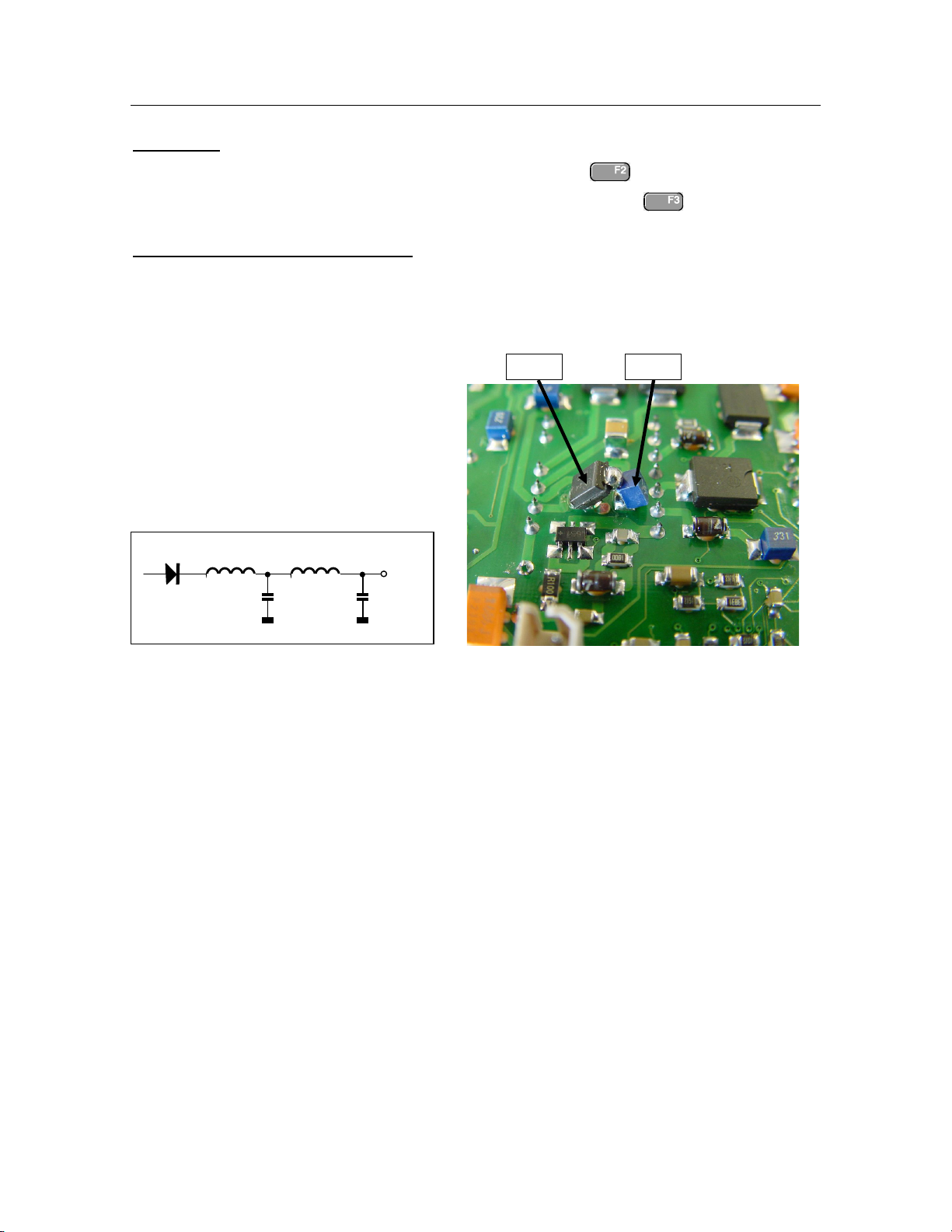
Add L4020, see the figures below.
L4020 is located in series with V4015 in the +5V2 supply on the Power Circuit. On the PCA one
side of V4015 is lifted and L4020 is mounted between the lifted side and the solder spot that
became free.
V4015 L4020
L4015
C4015
+5V2
C4016
Position of L4020 in Fig. 9-9 location D1 Position of L4020 in Fig. 9-14 location D2
2
Page 5

Table of Contents
Chapter Title Page
1 Safety Instructions ............................................................................. 1-1
1.1 Introduction................................................................................................. 1-3
1.2 Safety Precautions....................................................................................... 1-3
1.3 Caution and Warning Statements................................................................ 1-3
1.4 Symbols....................................................................................................... 1-3
1.5 Impaired Safety........................................................................................... 1-4
1.6 General Safety Information......................................................................... 1-4
2 Characteristics ................................................................................... 2-1
2.1 Introduction................................................................................................. 2-3
2.2 Dual Input Oscilloscope.............................................................................. 2-3
2.2.1 Isolated Inputs A and B (Vertical)....................................................... 2-3
2.2.2 Horizontal ............................................................................................ 2-4
2.2.3 Trigger and Delay................................................................................ 2-4
2.2.4 Automatic Connect&View Trigger ..................................................... 2-5
2.2.5 Edge Trigger ........................................................................................ 2-5
2.2.6 Isolated External Trigger ..................................................................... 2-5
2.2.7 Video Trigger....................................................................................... 2-5
2.2.8 Pulse Width Trigger............................................................................. 2-5
2.2.9 Continuous Auto Set............................................................................ 2-6
2.2.10 Automatic Capturing Scope Screens ................................................. 2-6
2.3 Automatic Scope Measurements................................................................. 2-6
2.3.1 General................................................................................................. 2-6
2.3.2 DC Voltage (VDC) .............................................................................. 2-6
2.3.3 AC Voltage (VAC) .............................................................................. 2-6
2.3.4 AC+DC Voltage (True RMS).............................................................. 2-7
2.3.5 Amperes (AMP)................................................................................... 2-7
2.3.6 Peak...................................................................................................... 2-8
2.3.7 Frequency (Hz) .................................................................................... 2-8
2.3.8 Duty Cycle (DUTY) ............................................................................ 2-8
2.3.9 Pulse Width (PULSE).......................................................................... 2-8
2.3.10 Vpwm (C versions only).................................................................... 2-8
2.3.11 Power ................................................................................................. 2-9
2.3.12 Phase .................................................................................................. 2-9
2.3.13 Temperature (TEMP) ........................................................................ 2-9
2.3.14 Decibel (dB)....................................................................................... 2-9
2.4 Meter ........................................................................................................... 2-10
2.4.1 Meter Input .......................................................................................... 2-10
2.4.2 Meter Functions................................................................................... 2-10
2.5 DMM Measurements on Meter Inputs........................................................ 2-10
2.5.1 General................................................................................................. 2-10
i
Page 6

Fluke 192B/196B-C/199B-C
Service Manual
2.5.2 Ohms (Ω) ............................................................................................. 2-10
2.5.3 Continuity (CONT).............................................................................. 2-10
2.5.4 Diode.................................................................................................... 2-11
2.5.5 Temperature (TEMP)........................................................................... 2-11
2.5.6 DC Voltage (VDC) .............................................................................. 2-11
2.5.7 AC Voltage (VAC) .............................................................................. 2-11
2.5.8 AC+DC Voltage (True RMS).............................................................. 2-11
2.5.9 Amperes (AMP)................................................................................... 2-12
2.6 Recorder ...................................................................................................... 2-12
2.6.1 TrendPlot (Meter or Scope)................................................................. 2-12
2.6.2 Scope Record ....................................................................................... 2-12
2.7 Zoom, Replay and Cursors.......................................................................... 2-13
2.7.1 Zoom.................................................................................................... 2-13
2.7.2 Replay .................................................................................................. 2-13
2.7.3 Cursor Measurements .......................................................................... 2-13
2.8 Miscellaneous.............................................................................................. 2-13
2.8.1 Display................................................................................................. 2-13
2.8.2
2.8.3 Probe Calibration................................................................................. 2-14
2.8.4 Memory................................................................................................ 2-14
2.8.5 Mechanical........................................................................................... 2-14
2.8.6 Optical Interface Port........................................................................... 2-14
2.9 Environmental............................................................................................. 2-14
2.10
2.11 10:1 probe VPS200 ................................................................................... 2-17
2.11.1 Safety ................................................................................................. 2-17
2.11.2 Electrical specifications..................................................................... 2-17
2.11.3 Environmental.................................................................................... 2-17
2.12 Electromagnetic Immunity........................................................................ 2-18
Power ............................................................................................ 2-13
Safety.................................................................................................. 2-15
3 Circuit Description ............................................................................. 3-1
3.1 Introduction................................................................................................. 3-3
3.2 Block Diagram ............................................................................................ 3-3
3.3 Start-up Sequence, Operating Modes.......................................................... 3-7
3.4 Detailed Circuit Descriptions...................................................................... 3-9
3.4.1 Scope Channel A - Scope Channel B .................................................. 3-9
3.4.2 Meter/Ext Trigger Channel.................................................................. 3-12
3.4.3 Sampling&Triggering (S-ASIC).......................................................... 3-15
3.4.4 S-ASIC supply ..................................................................................... 3-19
3.4.5 ADC’s .................................................................................................. 3-19
3.4.6 Digital Control..................................................................................... 3-20
3.4.7 LCD Control ........................................................................................ 3-22
3.4.8 Power ................................................................................................... 3-23
3.4.9 Slow ADC, RS232 Serial Interface, LCD Backlight........................... 3-28
4 Performance Verification................................................................... 4-1
4.1 Introduction................................................................................................. 4-3
4.2 Equipment Required For Verification ........................................................ 4-3
4.3 General Instructions .................................................................................... 4-3
4.4 Operating Instructions................................................................................. 4-4
4.4.1 Resetting the test tool .......................................................................... 4-4
4.4.2 Navigating through menu’s.................................................................. 4-4
4.4.3 Creating Test Tool Setup1................................................................... 4-5
4.5 Display and Backlight Test......................................................................... 4-5
ii
Page 7

Contents (continued)
4.6 Scope Input A&B Tests .............................................................................. 4-7
4.6.1 Input A&B Vertical Accuracy Test ..................................................... 4-7
4.6.2 Input A&B DC Voltage Accuracy Test............................................... 4-9
4.6.3 Input A&B AC Voltage Accuracy Test (LF)....................................... 4-11
4.6.4 Input A & B AC Coupled Lower Frequency Test.............................. 4-12
4.6.5 Input A and B Peak Measurements Test............................................. 4-13
4.6.6 Input A&B Frequency Measurement Accuracy Test .......................... 4-14
4.6.7 Input A&B Phase Measurements Test................................................. 4-15
4.6.8 Time Base Test .................................................................................... 4-16
4.6.9 Input A Trigger Sensitivity Test.......................................................... 4-18
4.6.10 Input A AC Voltage Accuracy (HF) & Bandwidth Test ................... 4-19
4.6.11 Input B Trigger Sensitivity Test ........................................................ 4-20
4.6.12 Input B AC Voltage Accuracy (HF) & Bandwidth Test ................... 4-21
4.6.13 Video test using the Video Pattern Generator ................................... 4-22
4.6.14 Video test using SC600 Scope Calibration Option ........................... 4-25
4.7 External Trigger Level Test ........................................................................ 4-27
4.8 Meter (DMM) Tests.................................................................................... 4-28
4.8.1 Meter DC Voltage Accuracy Test ....................................................... 4-28
4.8.2 Meter AC Voltage Accuracy & Frequency Response Test................ 4-29
4.8.3 Continuity Function Test ..................................................................... 4-30
4.8.4 Diode Test Function Test .................................................................... 4-30
4.8.5 Ohms Measurements Test.................................................................... 4-30
4.9 Probe Calibration Generator Test ............................................................... 4-32
5 Calibration Adjustment ...................................................................... 5-1
5.1 General ........................................................................................................ 5-3
5.1.1 Introduction.......................................................................................... 5-3
5.1.2 Calibration number and date................................................................ 5-3
5.1.3 General Instructions............................................................................. 5-3
5.1.4 Equipment Required For Calibration .................................................. 5-4
5.2 Calibration Procedure Steps........................................................................ 5-4
5.3 Starting the Calibration............................................................................... 5-4
5.4 Contrast Calibration Adjustment ................................................................ 5-6
5.5 Warming Up & Pre-Calibration.................................................................. 5-7
5.6 Final Calibration ......................................................................................... 5-8
5.6.1 Input A LF-HF Gain ............................................................................ 5-8
5.6.2 Input B LF-HF Gain............................................................................. 5-9
5.6.3 Input A&B LF-HF Gain....................................................................... 5-11
5.6.4 Input A&B Position ............................................................................ 5-12
5.6.5 Input A&B Volt Gain .......................................................................... 5-13
5.6.6 DMM Volt Gain .................................................................................. 5-14
5.6.7 Input A& B, and DMM Zero............................................................... 5-15
5.6.8 DMM Ohm Gain.................................................................................. 5-16
5.6.9 Calculate Gain.......................................................................................... 5-17
5.7 Save Calibration Data and Exit................................................................... 5-17
5.8 Probe Calibration ........................................................................................ 5-19
6 Disassembling the Test Tool............................................................. 6-1
6.1. Introduction................................................................................................ 6-3
6.2. Disassembly & Reassembly Procedures .................................................... 6-3
6.2.1 Required Tools .................................................................................... 6-3
6.2.2 Removing the Tilt Stand & Hang Strap............................................... 6-3
6.2.3 Replacing the Side-Strap, Changing the Side-Strap Position.............. 6-3
6.2.4 Opening the Test Tool, Removing the Battery.................................... 6-3
iii
Page 8

Fluke 192B/196B-C/199B-C
Service Manual
6.2.5 Removing the Main PCA Unit and the Fan......................................... 6-5
6.2.6 Removing the Display Assembly......................................................... 6-6
6.2.7 Replacing the LCD Window/Decal..................................................... 6-7
6.2.8 Removing the Keypad and Keypad Foil.............................................. 6-7
6.2.9 Disassembling the Main PCA Unit...................................................... 6-7
6.2.10 Reassembling the Main PCA Unit..................................................... 6-8
6.2.11 Reassembling the Test Tool............................................................... 6-9
7 Corrective Maintenance..................................................................... 7-1
7.1 Introduction................................................................................................. 7-3
7.2 Starting Fault Finding. ................................................................................ 7-4
7.3 Charger Circuit............................................................................................ 7-5
7.4 Starting with a Dead Test Tool ................................................................... 7-7
7.4.1 Test Tool Completely Dead................................................................. 7-7
7.4.2 Test Tool Software Does not Run. ...................................................... 7-8
7.4.3 Software Runs, Test Tool not Operative ............................................. 7-8
7.5 Miscellaneous Functions............................................................................. 7-8
7.5.1 Display and Back Light ....................................................................... 7-8
7.5.2 Fly Back Converter.............................................................................. 7-10
7.5.3 Slow ADC, +3V3SADC ...................................................................... 7-11
7.5.4 Keyboard.............................................................................................. 7-12
7.5.5 Optical Port (Serial RS232 Interface).................................................. 7-13
7.5.6 Channel A, Channel B Measurements................................................. 7-13
7.5.7 Meter Channel (Ext Trigger, Probe Cal) ............................................. 7-15
7.5.8 Input Signal Acquisition...................................................................... 7-17
7.5.9 ADC’s .................................................................................................. 7-19
7.5.10 Digital Control & Memory ................................................................ 7-20
7.5.11 Buzzer Circuit.................................................................................... 7-20
7.5.12 RAM Test .......................................................................................... 7-21
7.5.13 Power ON/OFF .................................................................................. 7-22
7.5.14 Battery................................................................................................ 7-22
7.6 Loading Software........................................................................................ 7-23
8 List of Replaceable Parts................................................................... 8-1
8.1 Introduction................................................................................................. 8-3
8.2 How to Obtain Parts.................................................................................... 8-3
8.3 Service Centers ........................................................................................... 8-3
8.4 Final Assembly Parts................................................................................... 8-4
8.5 Main PCA Unit Parts .................................................................................. 8-6
8.6 Main PCA Parts .......................................................................................... 8-8
8.7 Accessories.................................................................................................. 8-30
9 Circuit Diagrams ................................................................................ 9-1
9.1 Introduction................................................................................................. 9-3
9.2 Tracing signals in circuit diagrams............................................................. 9-3
9.3 Locating Parts & Test Points ...................................................................... 9-3
9.4 Diagrams ..................................................................................................... 9-6
10 Modifications...................................................................................... 10-1
10.1 General ...................................................................................................... 10-3
10.2 Software modifications ............................................................................. 10-3
10.3 Hardware modifications............................................................................ 10-3
10.4 Main PCA Unit Versions, Software Versions. ......................................... 10-4
iv
Page 9

List of Tables
Table Title Page
2-1. Scope No Visible Disturbance at E=3 V/m........................................................... 2-18
2-2. Scope Disturbance <10% at E=3 V/m................................................................... 2-18
2-3. Meter Disturbance <1% at 3 V/m ......................................................................... 2-18
3-1. Fluke190B-C Main Functional Blocks.................................................................. 3-3
3-2. Fluke190B-C Operating Modes ............................................................................ 3-8
3-3. D-ASIC PWM Signals........................................................................................... 3-22
4-1. Vertical Accuracy Verification Points .................................................................. 4-8
4-2. Volts DC Measurement Verification Points ......................................................... 4-10
4-4. Input A&B AC Input Coupling Verification Points.............................................. 4-13
4-5. Volts Peak Measurement Verification Points ....................................................... 4-14
4-6. Input A&B Frequency Measurement Accuracy Test ............................................ 4-15
4-7. Phase Measurement Verification Points ............................................................... 4-16
4-8. Input A Trigger Sensitivity Test Points................................................................. 4-18
4-9. HF AC Voltage Verification Points ...................................................................... 4-19
4-11. HF AC Voltage Verification Points ...................................................................... 4-21
4-12. Meter Volts dc Measurement Verification Points................................................. 4-28
4-13. Meter Volts AC Measurement Verification Points............................................... 4-29
4-14. Resistance Measurement Verification Points........................................................ 4-31
5-1. Input A HF-LF Gain Calibration Points................................................................ 5-9
5-2. Input B LF-HF Gain Calibration Points................................................................ 5-10
5-3. Input A&B Gain Calibration Points ...................................................................... 5-12
5-4. Input A&B Gain Calibration Points ...................................................................... 5-14
5-5. DMM Gain Calibration Points .............................................................................. 5-15
5-6. Ohm Gain Calibration Points ................................................................................ 5-17
7-1. Starting Fault Finding............................................................................................ 7-4
7-2. Test Tool Key Matrix............................................................................................ 7-12
7-3. Meter Channel Control Line Status....................................................................... 7-15
8-1. Final Assembly Parts............................................................................................. 8-4
8-2. Main PCA Unit Parts............................................................................................. 8-6
8-3. Main PCA Parts..................................................................................................... 8-8
8-4. Standard Accessories............................................................................................. 8-30
8-6. Users Manuals ....................................................................................................... 8-31
8-7. Optional Accessories............................................................................................. 8-31
9-1. Source & Destination of Signals ........................................................................... 9-4
9-2. Location of Test Points on PCA Top Side ............................................................ 9-5
9-2. Keyboard Layout................................................................................................... 9-6
9-3. Keyboard Layout................................................................................................... 9-6
v
Page 10

Fluke 192B/196B-C/199B-C
Service Manual
vi
Page 11

List of Figures
Figure Title Page
2-1 .Max. Input Voltage vs. Frequency ....................................................................... 2-16
2-2. Safe Handling: Max. Input Voltage Between Scope References, Between Scope
References and Meter Reference, and between Scope References/Meter Reference and earth
ground............................................................................................................................... 2-16
2-3. Max Voltage from Probe Tip to Ground and from Probe Tip to Probe Reference 2-17
3-1. Fluke190B-C Block Diagram................................................................................ 3-2
3-2. Fluke 190B-C Start-up Sequence, Operating Modes ............................................ 3-8
3-3. C-ASIC OQ0260 Block Diagram.......................................................................... 3-9
3-4. LF Floating to Non-Floating ................................................................................. 3-10
3-5. C-ASIC Control Circuit......................................................................................... 3-11
3-6. Meter/Ext Channel Block Diagram....................................................................... 3-12
3-7. S-ASIC signal section block diagram.................................................................... 3-15
3-8. S-ASIC Input Circuit ............................................................................................. 3-16
3-9. Trigger Circuit....................................................................................................... 3-17
3-10. Keyboard Control Signals ..................................................................................... 3-21
3-11. Power Supply Block Diagram............................................................................... 3-23
3-12. CHAGATE Control Voltage ................................................................................. 3-26
3-13. REFPWM2 circuit................................................................................................. 3-27
3-14. Fly-Back Converter Current and Control Voltage ................................................ 3-27
3-15. Back Light Converter Voltages............................................................................. 3-29
4-1. Menu item selection .............................................................................................. 4-4
4-3. Test Tool Input A&B to 5500 Normal Output...................................................... 4-7
4-4. 5500 Scope Output to Test Tool Input A&B ........................................................ 4-14
4-5. 5500A Scope Output to Test Tool Input A ........................................................... 4-16
4-7. 5500A Scope Output to Test Tool Input B............................................................ 4-20
4-8. Test Tool Input A to TV Signal Generator ........................................................... 4-22
4-9. Trace for PAL/SECAM line 622........................................................................... 4-23
4-10. Trace for NTSC line 525 ....................................................................................... 4-23
4-11. Trace for PAL/SECAM line 310........................................................................... 4-23
4-12. Trace for NTSC line 262 ....................................................................................... 4-23
4-13. Test Tool Input A to TV Signal Generator Inverted ............................................. 4-24
4-14. Trace for PAL/SECAM line 310 Negative Video................................................. 4-24
4-15. Trace for NTSC line 262 Negative Video............................................................. 4-24
4-16. Test Tool Input A to TV Signal Generator ........................................................... 4-25
4-17. SC600 Marker Pulse.............................................................................................. 4-26
4-18. Test Tool Meter/Ext Input to 5500A Normal Output ........................................... 4-27
4-19. Test Tool Input A to 5500A Normal Output 4-Wire............................................. 4-31
5-1. Version & Calibration Data................................................................................... 5-3
5-2. Display Test Pattern .............................................................................................. 5-7
5-3. 5500A SCOPE Output to Test Tool Input A......................................................... 5-8
5-4. 5500A SCOPE Output to Test Tool Input B......................................................... 5-10
5-5. Test tool Input A&B to 5500 Scope Output.......................................................... 5-11
5-6. Test tool Input A&B to 5500 Normal Output ....................................................... 5-13
vii
Page 12

Fluke 192B/196B-C/199B-C
Service Manual
5-7. 5500A NORMAL Output to Test Tool Banana Input........................................... 5-15
5-8. Four-wire Ohms calibration connections .............................................................. 5-16
5-9. 10:1 Probe Calibration Connection ....................................................................... 5-19
5-10. 10:1 Probe Calibration........................................................................................... 5-19
6-1. Loosen 2 Input Cover Screws................................................................................ 6-4
6-2. Loosen 2 Bottom Holster Screws.......................................................................... 6-4
6-3. Opening the Test Tool........................................................................................... 6-4
6-4. Removing the Battery Pack................................................................................... 6-4
6-5. Final Assembly Details.......................................................................................... 6-5
6-6. Flex Cable Connectors .......................................................................................... 6-6
6-7. PCA Unit Assembly .............................................................................................. 6-8
7-1. Operative Test Tool without Case......................................................................... 7-4
7-2. Supply voltages PCB TOP .................................................................................... 7-10
7-3. Supply voltages PCB bottom................................................................................. 7-10
8-1. Final Assembly Details.......................................................................................... 8-5
8-2. New version bottom cover..................................................................................... 8-6
8-3. Bottom cover old, NOT for 192B, 196B-C,-199B-C ............................................ 8-6
8-4. Main PCA Unit...................................................................................................... 8-7
8-5. Rubber Spacer on Shielding Box Assy ................................................................. 8-7
9-1. Scope Channel A ................................................................................................... 9-7
9-2. Scope Channel B ................................................................................................... 9-8
9-3. Meter/External TriggerChannel ............................................................................ 9-9
9-4. Sample & Trigger Circuit...................................................................................... 9-10
9-5. S-ASIC Supply ...................................................................................................... 9-11
9-6. ADC’s.................................................................................................................... 9-12
9-7. Digital Control....................................................................................................... 9-13
9-8. LCD Control & Supply Circuit ............................................................................. 9-14
9-9. Power Circuit......................................................................................................... 9-15
9-10. Backlight, Slow ADC, Serial Interface ................................................................. 9-16
9-11. OLD Main PCA Top View.................................................................................... 9-17
9-12. OLD Main PCA Bottom View .............................................................................. 9-18
9-13. NEW Main PCA Top View................................................................................... 9-19
9-14. NEW Main PCA Bottom View ............................................................................. 9-20
10-1. PCA revision number sticker................................................................................. 10-3
viii
Page 13

Chapter 1
Safety Instructions
Title Page
1.1 Introduction................................................................................................. 1-3
1.2 Safety Precautions....................................................................................... 1-3
1.3 Caution and Warning Statements................................................................ 1-3
1.4 Symbols....................................................................................................... 1-3
1.5 Impaired Safety........................................................................................... 1-4
1.6 General Safety Information......................................................................... 1-4
1-1
Page 14

Page 15
1.1 Introduction
Read these pages carefully before beginning to install and use the test tool.
The following paragraphs contain information, cautions and warnings which must be
followed to ensure safe operation and to keep the test tool in a safe condition.
Servicing described in this manual is to be done only by
qualified service personnel. To avoid electrical shock, do not
service the test tool unless you are qualified to do so.
1.2 Safety Precautions
For the correct and safe use of this test tool it is essential that both operating and service
personnel follow generally accepted safety procedures in addition to the safety
precautions specified in this manual. Specific warning and caution statements, where
they apply, will be found throughout the manual. Where necessary, the warning and
caution statements and/or symbols are marked on the test tool.
Warning
Safety Instructions
1.1 Introduction
1
1.3 Caution and Warning Statements
Caution
Used to indicate correct operating or maintenance procedures
to prevent damage to or destruction of the equipment or other
property.
Warning
Calls attention to a potential danger that requires correct
procedures or practices to prevent personal injury.
1.4 Symbols
The following symbols are used on the test tool, in the Users Manual, in this Service
Manual, or on spare parts for this test tool.
See explanation in Users Manual DOUBLE INSULATION (Protection
Live voltage Earth Ground
Static sensitive components
(black/yellow).
Class)
Recycling information
Disposal information Conformité Européenne
Safety Approval Safety Approval
1-3
Page 16

Fluke 192B/196B-C/199B-C
Service Manual
1.5 Impaired Safety
Whenever it is likely that safety has been impaired, the test tool must be turned off and
disconnected from line power. The matter should then be referred to qualified
technicians. Safety is likely to be impaired if, for example, the test tool fails to perform
the intended measurements or shows visible damage.
1.6 General Safety Information
Removing the test tool covers or removing parts, except those
to which access can be gained by hand, is likely to expose live
parts and accessible terminals which can be dangerous to life.
The test tool shall be disconnected from all voltage sources before it is opened.
Capacitors inside the test tool can hold their charge even if the test tool has been
separated from all voltage sources.
When servicing the test tool, use only specified replacement parts.
Warning
1-4
Page 17

Chapter 2
Characteristics
Title Page
2.1 Introduction................................................................................................. 2-3
2.2 Dual Input Oscilloscope.............................................................................. 2-3
2.2.1 Isolated Inputs A and B (Vertical)....................................................... 2-3
2.2.2 Horizontal ............................................................................................ 2-4
2.2.3 Trigger and Delay................................................................................ 2-4
2.2.4 Automatic Connect&View Trigger ..................................................... 2-5
2.2.5 Edge Trigger ........................................................................................ 2-5
2.2.6 Isolated External Trigger ..................................................................... 2-5
2.2.7 Video Trigger....................................................................................... 2-5
2.2.8 Pulse Width Trigger............................................................................. 2-5
2.2.9 Continuous Auto Set............................................................................ 2-6
2.2.10 Automatic Capturing Scope Screens ................................................. 2-6
2.3 Automatic Scope Measurements................................................................. 2-6
2.3.1 General................................................................................................. 2-6
2.3.2 DC Voltage (VDC) .............................................................................. 2-6
2.3.3 AC Voltage (VAC) .............................................................................. 2-6
2.3.4 AC+DC Voltage (True RMS).............................................................. 2-7
2.3.5 Amperes (AMP)................................................................................... 2-7
2.3.6 Peak...................................................................................................... 2-8
2.3.7 Frequency (Hz) .................................................................................... 2-8
2.3.8 Duty Cycle (DUTY) ............................................................................ 2-8
2.3.9 Pulse Width (PULSE).......................................................................... 2-8
2.3.10 Vpwm (C versions only).................................................................... 2-8
2.3.11 Power ................................................................................................. 2-9
2.3.12 Phase .................................................................................................. 2-9
2.3.13 Temperature (TEMP) ........................................................................ 2-9
2.3.14 Decibel (dB)....................................................................................... 2-9
2.4 Meter ........................................................................................................... 2-10
2.4.1 Meter Input .......................................................................................... 2-10
2.4.2 Meter Functions................................................................................... 2-10
2-1
Page 18

Fluke 192B/196B-C/199B-C
Service Manual
2.5 DMM Measurements on Meter Inputs........................................................ 2-10
2.6 Recorder ...................................................................................................... 2-12
2.7 Zoom, Replay and Cursors.......................................................................... 2-13
2.8 Miscellaneous ............................................................................................. 2-13
2.9 Environmental............................................................................................. 2-14
2.10
2.11 10:1 probe VPS200 ................................................................................... 2-17
2.12 Electromagnetic Immunity........................................................................ 2-18
2.5.1 General................................................................................................. 2-10
2.5.2 Ohms (Ω) ............................................................................................. 2-10
2.5.3 Continuity (CONT).............................................................................. 2-10
2.5.4 Diode.................................................................................................... 2-11
2.5.5 Temperature (TEMP) .......................................................................... 2-11
2.5.6 DC Voltage (VDC) .............................................................................. 2-11
2.5.7 AC Voltage (VAC) .............................................................................. 2-11
2.5.8 AC+DC Voltage (True RMS).............................................................. 2-11
2.5.9 Amperes (AMP)................................................................................... 2-12
2.6.1 TrendPlot (Meter or Scope)................................................................. 2-12
2.6.2 Scope Record ....................................................................................... 2-12
2.7.1 Zoom.................................................................................................... 2-13
2.7.2 Replay .................................................................................................. 2-13
2.7.3 Cursor Measurements .......................................................................... 2-13
2.8.1 Display................................................................................................. 2-13
2.8.2
Power ............................................................................................ 2-13
2.8.3 Probe Calibration................................................................................. 2-14
2.8.4 Memory................................................................................................ 2-14
2.8.5 Mechanical........................................................................................... 2-14
2.8.6 Optical Interface Port........................................................................... 2-14
Safety.................................................................................................. 2-15
2.11.1 Safety ................................................................................................. 2-17
2.11.2 Electrical specifications..................................................................... 2-17
2.11.3 Environmental.................................................................................... 2-17
2-2
Page 19

2.1 Introduction
Performance Characteristics
FLUKE guarantees the properties expressed in numerical values with the stated
tolerance. Specified non-tolerance numerical values indicate those that could be
nominally expected from the mean of a range of identical ScopeMeter test tools.
Environmental Data
The environmental data mentioned in this manual are based on the results of the
manufacturer’s verification procedures.
Safety Characteristics
The test tool has been designed and tested in accordance with Standards ANSI/ISA
S82.01-1994, EN 61010.1 (1993) (IEC 1010-1), CAN/CSA-C22.2 No.1010.1-92
(including approval), UL3111-1 (including approval) Safety Requirements for Electrical
Equipment for Measurement, Control, and Laboratory Use.
This manual contains information and warnings that must be followed by the user to
ensure safe operation and to keep the instrument in a safe condition. Use of this
equipment in a manner not specified by the manufacturer may impair protection provided
by the equipment.
Characteristics
2.1 Introduction
2
2.2 Dual Input Oscilloscope
2.2.1 Isolated Inputs A and B (Vertical)
Bandwidth, DC Coupled
FLUKE 199B-C.......................................... 200 MHz (-3 dB)
FLUKE 196B-C.......................................... 100 MHz (-3 dB)
FLUKE 192B.............................................. 60 MHz (-3 dB)
Lower Frequency Limit, AC Coupled
with 10:1 probe........................................... <2 Hz (-3 dB)
direct (1:1) .................................................. <5 Hz (-3 dB)
Rise Time (typical, calculated)
FLUKE 199B-C.......................................... 1.7 ns
FLUKE 196B-C.......................................... 3.5 ns
FLUKE 192B.............................................. 5.8 ns
Analog Bandwidth Limiters ............................ 20 MHz and 10 kHz
Input Coupling................................................. AC, DC
Polarity............................................................. Normal, Inverted
Sensitivity Ranges C Versions, software V5.04 and higher
with 10:1 probe........................................... 20 mV to 1000 V/div
direct (1:1) .................................................. 2 mV to 100 V/div
Sensitivity Ranges B Versions, and C versions software below V5.04
with 10:1 probe........................................... 50 mV to 1000 V/div
direct (1:1) .................................................. 5 mV to 100 V/div
Trace Positioning Range.................................. ±4 divisions
Input Impedance on BNC
DC Coupled ................................................ 1 MΩ (±1 %)//15 pF (±2 pF)
2-3
Page 20

Fluke 192B/196B-C/199B-C
Service Manual
Max. Input Voltage
with 10:1 probe........................................... 600 V CAT III, 1000 V CAT II
direct (1:1) .................................................. 300 V CAT III
Vertical Accuracy............................................ ±(1.5 % + 0.04 range/div)
Digitizer Resolution......................................... 8 bits, separate digitizer for each input
2.2.2 Horizontal
Maximum Time Base Speed:
FLUKE 199B-C.......................................... 5 ns/div
FLUKE 196B-C.......................................... 5 ns/div
FLUKE 192B.............................................. 10 ns/div
Minimum Time Base Speed (Scope Record) .. 2 min/div
(For detailed specifications, see “Safety”)
±(2.5 % + 0.08 range/div) for 2 mV/div
range
For voltage measurements with 10:1
probe, add probe accuracy, see section
’10:1 Probe’ on page 17
Real Time Sampling Rate (for both inputs simultaneously):
FLUKE199B-C:
5 ns to 2 µs /div .....................................up to 2.5 GS/s
5 µs to 120 s/div ....................................20 MS/s
FLUKE 196B-C:
5 ns to 2 µs /div .....................................up to 1 GS/s
5 µs to 120 s/div ....................................20 MS/s
FLUKE 192B:
10 ns to 2 µs /div ...................................up to 500 MS/s
5 µs to 120 s/div ....................................20 MS/s
Record Length
Scope Record Mode....................................
Scope Normal Mode................................... ≤ 1200 points on each input
Scope Glitch Capture Mode .......................300 min/max pairs on each input
Glitch Detection
2 µs to 120 s/div.......................................... displays glitches as fast as 50 ns
Waveform Display........................................... A, B, A+B, A-B, A*B, A vs. B
Time Base Accuracy........................................ ± (100 ppm + 1 pixel)
2.2.3 Trigger and Delay
≥=27000 points on each input
Normal, Average (2,4,8,64x), Persistence
2-4
Trigger Modes ................................................. Automatic, Edge, External, Video,
Pulse Width
Trigger Delay................................................... up to +1200 divisions
Pre Trigger View ............................................. one full screen length
Max. Delay ......................................................12 seconds
Page 21

2.2.4 Automatic Connect&View Trigger
Source .............................................................. A, B, EXT
Slope ................................................................ Positive, Negative
2.2.5 Edge Trigger
Screen Update.................................................. Free Run, On Trigger, Single Shot
Source .............................................................. A, B, EXT
Slope ................................................................ Positive, Negative
Trigger Level Control Range........................... ±4 divisions
Trigger Sensitivity A and B
DC to 5 MHz at >5 mV/div........................ 0.5 divisions
DC to 5 MHz at 2 mV/div & 5 mV/div...... 1 division
200 MHz (FLUKE 199B-C)....................... 1 division
250 MHz (FLUKE 199B-C)....................... 2 divisions
100 MHz (FLUKE 196B-C)....................... 1 division
150 MHz (FLUKE 196B-C)....................... 2 divisions
60 MHz (FLUKE 192B)............................. 1 division
100 MHz (FLUKE 192B)........................... 2 divisions
Characteristics
2.2 Dual Input Oscilloscope
2
2.2.6 Isolated External Trigger
Bandwidth........................................................ 10 kHz
Modes ..............................................................Automatic, Edge
Trigger Levels (DC to 10 kHz) 120 mV, 1.2 V
2.2.7 Video Trigger
Standards .........................................................PAL, PAL+, NTSC, SECAM
Modes ..............................................................Lines, Line Select, Field 1 or Field 2
Source .............................................................. A
Polarity............................................................. Positive, Negative
Sensitivity ........................................................ 0.7 division sync level
2.2.8 Pulse Width Trigger
Screen Update.................................................. On Trigger, Single Shot
Trigger Conditions........................................... <T, >T, =T (±10 %), ≠T(±10 %)
Source .............................................................. A
Polarity............................................................. Positive or negative pulse
Pulse Time Adjustment Range ........................ 0.01 div. to 655 div.
with a minimum value of 300 ns (<T, >T) or 500 ns (=T, ≠T),
a maximum value of 10 s,
and a resolution of 0.01 div. with a minimum value of 50 ns.
2-5
Page 22

Fluke 192B/196B-C/199B-C
Service Manual
2.2.9 Continuous Auto Set
Autoranging attenuators and time base, automatic Connect&View™ triggering with
automatic source selection.
Modes
Normal ........................................................ 15 Hz to max. bandwidth
Low Frequency ........................................... 1 Hz to max. bandwidth
Minimum Amplitude A and B
DC to 1 MHz ..............................................10 mV
1 MHz to max. bandwidth .......................... 20 mV
2.2.10 Automatic Capturing Scope Screens
Capacity........................................................... 100 dual input scope Screens
2.3 Automatic Scope Measurements
The accuracy of all readings is within ± (% of reading + number of counts) from 18 °C to
28 °C. Add 0.1x (specific accuracy) for each °C below 18 °C or above 28 °C. For
voltage measurements with 10:1 probe, add probe accuracy, see section ’10:1 Probe’ on
page 17. At least 1.5 waveform period must be visible on the sceen.
For viewing screens, see Replay function.
2.3.1 General
Inputs ............................................................... A and B
DC Common Mode Rejection (CMRR).......... >100 dB
AC Common Mode Rejection ........................ >60 dB at 50, 60, or 400 Hz
2.3.2 DC Voltage (VDC)
Maximum Voltage
with 10:1 probe........................................... 1000 V
direct (1:1) .................................................. 300 V
Maximum Resolution
with 10:1 probe........................................... 1 mV
direct (1:1) .................................................. 100 µV
Full Scale Reading........................................... 1100 counts
Accuracy at 5 s to 5 µs/div .............................. ±(1.5 % +5 counts)
Normal Mode AC Rejection at 50 or 60 Hz ... >60 dB
2.3.3 AC Voltage (VAC)
Maximum Voltage
with 10:1 probe........................................... 1000 V
direct (1:1) .................................................. 300 V
±(1.5% + 10 counts) for 2 mV/div
2-6
Page 23

Characteristics
2.3 Automatic Scope Measurements
Maximum Resolution
with 10:1 probe........................................... 1 mV
direct (1:1) .................................................. 100 µV
Full Scale Reading........................................... 1100 counts
Accuracy
DC coupled:
DC to 60 Hz........................................... ±(1.5 % +10 counts)
AC coupled, low frequencies:
50 Hz direct (1:1)................................... ±(2.1 % + 10 counts)
60 Hz direct (1:1)................................... ±(1.9 % + 10 counts)
With the 10:1 probe the low frequency roll off point will be lowered to 2 Hz, which
improves the AC accuracy for low frequencies. When possible use DC coupling for
maximum accuracy.
AC or DC coupled, high frequencies:
60 Hz to 20 kHz..................................... ±(2.5 % +15 counts)
20 kHz to 1 MHz ................................... ±(5 % +20 counts)
1 MHz to 25 MHz.................................. ±(10 % +20 counts)
For higher frequencies the instrument’s frequency roll off starts affecting accuracy.
2
Normal Mode DC Rejection............................ >50 dB
All accuracies are valid if:
• The waveform amplitude is larger than one division
• At least 1.5 waveform period is on the screen
2.3.4 AC+DC Voltage (True RMS)
Maximum Voltage
with 10:1 probe........................................... 1000 V
direct (1:1) .................................................. 300 V
Maximum Resolution
with 10:1 probe........................................... 1 mV
direct (1:1) .................................................. 100 µV
Full Scale Reading........................................... 1100 counts
Accuracy
DC to 60 Hz................................................ ±(1.5 % +10 counts)
60 Hz to 20 kHz.......................................... ±(2.5 % +15 counts)
20 kHz to 1 MHz ........................................ ±(5 % +20 counts)
1 MHz to 25 MHz....................................... ±(10 % +20 counts)
For higher frequencies the instrument’s frequency roll off starts affecting accuracy.
2.3.5 Amperes (AMP)
With Optional Current Probe or Current Shunt
Ranges ............................................................. same as VDC, VAC, VAC+DC
Probe Sensitivity.............................................. 100 µV/A, 1 mV/A, 10 mV/A, 100 mV/A,
Accuracy.......................................................... same as VDC, VAC, VAC+DC
1 V/A, 10 V/A, and 100 V/A
(add current probe or -shunt accuracy)
2-7
Page 24

Fluke 192B/196B-C/199B-C
Service Manual
2.3.6 Peak
Modes ..............................................................Max peak, Min peak, or pk-to-pk
Maximum Voltage
with 10:1 probe........................................... 1000 V
direct (1:1) .................................................. 300 V
Maximum Resolution
with 10:1 probe........................................... 10 mV
direct (1:1) .................................................. 1 mV
Full Scale Reading........................................... 800 counts
Accuracy
Max peak or Min peak................................ ±0.2 division
Peak-to-peak ............................................... ±0.4 division
2.3.7 Frequency (Hz)
Range ............................................................... 1.000 Hz to full bandwidth
Full Scale Reading........................................... 9 999 counts, with at least 10 waveform
periods on screen.
Accuracy
1 Hz to full bandwidth................................ ±(0.5 % +2 counts)
2.3.8 Duty Cycle (DUTY)
Range ............................................................... 4.0 % to 98.0 %
2.3.9 Pulse Width (PULSE)
Resolution........................................................ 1/100 division
Full Scale Reading........................................... 999 counts
Accuracy
1 Hz to full bandwidth................................ ±(0.5 % +2 counts)
2.3.10 Vpwm (C versions only)
Purpose ............................................................to measure on pulse width modulated
Principle........................................................... readings show the effective voltage based
Accuracy.......................................................... as Vrms for sinewave signals
signals, like motor drive inverter outputs
on the average value of samples, over a
whole number of periods of the
fundamental frequency
2-8
Page 25

2.3.11 Power
Power Factor.................................................... ratio between Watts and VA
Range .......................................................... 0.00 to 1.00
Watt ............................................................... RMS reading of multiplication
Full Scale Reading...................................... 999 counts
VA ............................................................... Vrms x Arms
Full Scale Reading...................................... 999 counts
VA Reactive ....................................................√((VA)
Full Scale Reading...................................... 999 counts
2.3.12 Phase
Range ............................................................... -180 to +180 degrees
Resolution........................................................ 1 degree
Accuracy
0.1 Hz to 1 MHz ......................................... ±2 degrees
1 MHz to 10 MHz....................................... ±3 degrees
Characteristics
2.3 Automatic Scope Measurements
corresponding samples Input A (volts)
and Input B (amperes)
2-W2
)
2
2.3.13 Temperature (TEMP)
With Optional Temperature Probe
Ranges (°C or °F) ............................................-40.0 to +100.0 °
Probe Sensitivity.............................................. 1 mV/°C and 1 mV/°F
Accuracy.......................................................... as VDC (add temp. probe accuracy)
2.3.14 Decibel (dB)
dBV ............................................................... dB relative to one volt
dBm ............................................................... dB relative to one mW in 50 Ω or 600 Ω
dBon ...............................................................VDC, VAC, or VAC+DC
Accuracy.......................................................... same as VDC, VAC, VAC+DC
-100 to +250 °
-100 to +500 °
-100 to +1000 °
-100 to + 2500 °
2-9
Page 26

Fluke 192B/196B-C/199B-C
Service Manual
2.4 Meter
2.4.1 Meter Input
Input Coupling................................................. DC
Frequency Response........................................ DC to 10 kHz (-3 dB)
Input Impedance .............................................. 1 MΩ (±1 %)//10 pF (±1.5 pF)
Max. Input Voltage ................................... 1000 V CAT II, 600 V CAT III
2.4.2 Meter Functions
Ranging............................................................ Auto, Manual
Modes ..............................................................Normal, Relative
2.5 DMM Measurements on Meter Inputs
(For detailed specifications, see “Safety”)
The accuracy of all measurements is within ± (% of reading + number of counts) from
18 °C to 28 °C.
Add 0.1x (specific accuracy) for each °C below 18 °C or above 28 °C.
2.5.1 General
DC Common Mode Rejection (CMRR).......... >100 dB
AC Common Mode Rejection ......................... >60 dB at 50, 60, or 400 Hz
2.5.2 Ohms (
Ranges ............................................................. 500.0 Ω, 5.000 kΩ, 50.00 kΩ,
Full Scale Reading
500 Ω to 5 MΩ ........................................... 5000 counts
30 MΩ......................................................... 3000 counts
Accuracy.......................................................... ±(0.6 % +5 counts)
Measurement Current ...................................... 0.5 mA to 50 nA, ±20 %
Open Circuit Voltage....................................... <4 V
ΩΩΩΩ
)
500.0 kΩ, 5.000 MΩ, 30.00 MΩ
decreases with increasing ranges
2.5.3 Continuity (CONT)
Beep ............................................................... <50 Ω (±30 Ω)
Measurement Current ...................................... 0.5 mA, ±20 %
Detection of shorts of ......................................≥1 ms
2-10
Page 27

2.5.4 Diode
Maximum Voltage Reading............................. 2.8 V
Open Circuit Voltage....................................... <4 V
Accuracy.......................................................... ±(2 % +5 counts)
Measurement Current ...................................... 0.5 mA, ±20 %
2.5.5 Temperature (TEMP)
With Optional Temperature Probe
Ranges (°C or °F) ............................................-40.0 to +100.0 ° ; -100.0 to +250.0 ° ;
Probe Sensitivity.............................................. 1 mV/°C and 1 mV/°F
Accuracy.......................................................... as VDC (add temp. probe accuracy)
2.5.6 DC Voltage (VDC)
Ranges ............................................................. 500.0 mV, 5.000 V, 50.00 V, 500.0 V,
Characteristics
2.5 DMM Measurements on Meter Inputs
-100.0 to +500.0 ° ; -100 to +1000 °
-100 to + 2500 °
1100 V
2
Full Scale Reading........................................... 5000 counts
Accuracy.......................................................... ±(0.5 % +5 counts)
Normal Mode AC Rejection............................ >60 dB at 50 or 60 Hz ±1 %
2.5.7 AC Voltage (VAC)
Ranges ............................................................. 500.0 mV, 5.000 V, 50.00 V, 500.0 V,
Full Scale Reading........................................... 5000 counts
Accuracy
15 Hz to 60 Hz............................................ ±(1 % +10 counts)
60 Hz to 1 kHz............................................ ±(2.5 % +15 counts)
For higher frequencies the frequency roll off of the Meter input starts affecting
accuracy.
Normal Mode DC Rejection............................ >50 dB
2.5.8 AC+DC Voltage (True RMS)
Ranges ............................................................. 500.0 mV, 5.000 V, 50.00 V, 500.0 V,
Full Scale Reading........................................... 5000 counts
1100 V
1100 V
Accuracy
DC to 60 Hz................................................ ±(1 % +10 counts)
60 Hz to 1 kHz............................................ ±(2.5 % +15 counts)
For higher frequencies the frequency roll off of the Meter input starts affecting
accuracy.
All accuracies are valid if the waveform amplitude is larger than 5 % of full scale.
2-11
Page 28

Fluke 192B/196B-C/199B-C
Service Manual
2.5.9 Amperes (AMP)
With Optional Current Probe or Current Shunt.
Ranges ............................................................. same as VDC, VAC, VAC+DC
Probe Sensitivity.............................................. 100 µV/A, 1 mV/A, 10 mV/A, 100 mV/A,
Accuracy.......................................................... same as VDC, VAC, VAC+DC
2.6 Recorder
2.6.1 TrendPlot (Meter or Scope)
Chart recorder that plots a graph of min and max values of Meter or Scope measurements
over time.
Measurement Speed......................................... > 5 measurements/s
Time/Div.......................................................... 5 s/div to 30 min/div
1 V/A, 10 V/A, and 100 V/A
(add current probe or -shunt accuracy)
Record Size...................................................... 18000 points
Recorded Time Span ....................................... 60 min to 22 days (single reading)
Time Reference................................................ time from start, time of day
2.6.2 Scope Record
Records scope waveforms in deep memory while displaying the waveform in Roll mode.
Source .............................................................. Input A, Input B
Max. Sample Speed (5 ms/div to 1 min/div) ... 20 MS/s
Glitch capture (5 ms/div to 1 min/div) ............50 ns
Time/Div in normal mode ............................... 5 ms/div to 2 min/div
Record Size...................................................... 27000 points per input
Recorded Time Span ....................................... 6 s to 48 hours
Acquisition Modes........................................... Single Sweep
Time Reference................................................ time from start, time of day
30 min to 11 days (dual reading)
Continuous Roll
External Triggering
2-12
Page 29

2.7 Zoom, Replay and Cursors
2.7.1 Zoom
Horizontal Magnification
Scope Record.............................................. up to 120x
TrendPlot .................................................... up to 96x
Scope .......................................................... up to 8x
2.7.2 Replay
Displays a maximum of 100 captured dual input Scope screens.
Replay modes Step by Step, Replay as Animation
2.7.3 Cursor Measurements
Cursor Modes ..................................................single vertical cursor
Characteristics
2.7 Zoom, Replay and Cursors
dual vertical cursors
dual horizontal cursors (Scope mode)
2
Markers............................................................ automatic markers at cross points
Measurements.................................................. value at cursor 1
2.8 Miscellaneous
2.8.1 Display
View Area........................................................ 115 x 86 mm (4.5 x 3.4 inches)
Backlight.......................................................... Cold Cathode Fluorescent (CCFL)
Brightness C-versions B-Versions
Power Adapter: .......................................... 80 cd / m
Batteries...................................................... 50 cd / m
2.8.2 Power
value at cursor 2
difference between values at cursor 1 & 2
time between cursors
Time of Day (Recorder modes)
Time from Start (Recorder modes)
Rise Time
Temperature compensated
2
125 cd / m
2
75 cd / m
2
2
Rechargeable NiMH Batteries:
Operating Time........................................... 4 hours
Charging Time............................................ 4 hours
Allowable ambient temperature
during charging........................................... 0 to 40 °C (32 to 104 °F)
Auto power down time (battery saving)..... 5 min, 30 min or disabled
2-13
Page 30

Fluke 192B/196B-C/199B-C
Service Manual
Battery Charger / Power Adapter BC190:
• BC190/801 Universal European line plug 230 V ±10 %
• BC190/803 North American line plug 120 V ±10 %
• BC190/804 United Kingdom line plug 230 V ±10 %
• BC190/806 Japanese line plug 100 V ±10 %
• BC190/807 Australian line plug 230 V ±10 %
• BC190/808 Universal switchable adapter 115 V ±10 % or 230 V ±10 %,
with plug EN60320-2.2G
Line Frequency................................................ 50 and 60 Hz.
2.8.3 Probe Calibration
Manual pulse adjustment and automatic DC adjustment with probe check.
Generator Output ............................................. 3 Vpp / 500 Hz square wave
2.8.4 Memory
Number of Scope Memories............................ 10
Each memory can contain two waveforms plus corresponding setups
Number of Recorder Memories....................... 2
Each memory can contain:
• a dual input TrendPlot (2 x 9000 points)
• a dual input Scope Record (2 x 27000 points)
• 100 dual input Scope screens
2.8.5 Mechanical
Size ...............................................................64 x 169 x 256 mm (2.5 x 6.6 x 10.1 in)
Weight .............................................................2 kg (4.4 lbs) including battery
2.8.6 Optical Interface Port
Via RS-232, optically isolated
To Printer
Supports Epson FX, LQ, HP Deskjet®, Laserjet®, and Postscript
Serial via PM9080 (optically isolated RS-232 adapter/cable, optional).
Parallel via PAC91 (optically isolated Print Adapter Cable, optional).
To PC/Notebook
Serial via PM9080 (optically isolated RS-232 adapter/cable, optional), using SW90W
(FlukeView software for Windows).
2.9 Environmental
Environmental .................................................MIL-PRF-28800F, Class 2
Temperature
Operating:
battery operated ..................................... 0 to 50 °C (32 to 122 °F)
power operated ......................................0 to 40 °C (32 to 104 °F)
Storage ........................................................ -20 to +60 °C (-4 to +140 °F)
2-14
Page 31

Humidity
Operating:
0 to 10 °C (32 to 50 °F) ......................... noncondensing
10 to 30 °C (50 to 86 °F) ....................... 95 %
30 to 40 °C (86 to 104 °F) ..................... 75 %
40 to 50 °C (104 to 122 °F) ................... 45 %
Storage:
-20 to 60 °C (-4 to 140 °F)..................... noncondensing
Altitude
Operating .................................................... 3 km (10 000 feet)
Storage ........................................................ 12 km (40 000 feet)
Vibration (sinusoidal)...................................... max. 3 g
Shock ............................................................... max. 30 g
Electromagnetic Compatibility (EMC)
Emission and immunity EN-IEC61326-1 (1997)
Enclosure Protection........................................ IP51, ref: IEC529
2.10 Safety
Characteristics
2.10 Safety
2
Designed for measurements on 1000 V Category II Installations, 600 V Category III
Installations, Pollution Degree 2, per:
• ANSI/ISA S82.01-1994
• EN61010-1 (1993) (IEC1010-1)
• CAN/CSA-C22.2 No.1010.1-92
• UL3111-1
Max. Input Voltages
Input A and B directly ................................ 300 V CAT III
Input A and B via 10:1 probe .....................1000 V CAT II, 600 V CAT III
METER/EXT TRIG inputs......................... 1000 V CAT II, 600 V CAT III
Max. Floating Voltage
from any terminal to ground....................... 1000 V CAT II, 600 V CAT III
between any terminal.................................. 1000 V CAT II, 600 V CAT III
Voltage ratings are given as “working voltage”. They should be read as Vac-rms
(50-60 Hz) for AC sinewave applications and as Vdc for DC applications.
2-15
Page 32

Fluke 192B/196B-C/199B-C
)
)
Service Manual
}
Figure 2-1. Max. Input Voltage vs. Frequency
190-volt-f req.wmf
Note
Overvoltage Category III refers to distribution level and fixed installation
circuits inside a building. Overvoltage Category II refers to local level,
which is applicable for appliances and portable equipment.
VOLTAGE (Vrms
30
FREQUENCY (kHz
Figure 2-2. Safe Handling: Max. Input Voltage Between Scope References, Between Scope
References and Meter Reference, and between Scope References/Meter Reference and earth ground
190-safe-handling.W MF
2-16
Page 33

2.11 10:1 probe VPS200
T
2.11.1 Safety
Max. Input Voltage................................... 1000 V CAT II, 600 V CAT III
Max. Floating Voltage
from any terminal to ground....................... 1000 V CAT II, 600 V CAT II
2.11.2 Electrical specifications
Input Impedance at probe tip........................... 10 MΩ (±2 %)//14 pF (±2 pF)
Capacity Adjustment Range ............................ 10 to 22 pF
Attenuation at DC (1 MΩ input) ..................... 10 x
Bandwidth (with Fluke 199C) ......................... DC to 200 MHz (-3 dB)
Probe accuracy when adjusted on the test tool
DC to 20kHz............................................... 1%
AC 20kHz to 1MHz.................................... 2%
AC 1MHz to 25MHz .................................. 3%
For higher freqeuncies the probe’s frequency roll off starts affecting the accuracy.
Characteristics
2.11 10:1 probe VPS200
2
2.11.3 Environmental
Temperature
Operating .................................................... 0 to 50 °C (32 to 122 °F)
Storage ........................................................ -20 to +60 °C (-4 to 140 °F)
Altitude
Operating .................................................... 3 km (10 000 feet)
Storage ........................................................ 12 km (40 000 feet)
Humidity
Operating at 10 to 30 °C (50 to 86 °F) .......95 %
MAX. I NPU
VOLTAGE (Vrm s)
1000
500
200
100
50
20
10
5
2
1
0.01
0.02 0.05 0.1 0.2 0.5 1 2 5 10 20 50 100 200
Figure 2-3. Max Voltage from VPS200 Probe Tip to Ground and from VPS200 Probe Tip to Probe
Reference
CAT II
CAT III
FREQUENCY (MHz)
ST8696.WMF
2-17
Page 34

Fluke 192B/196B-C/199B-C
Service Manual
2.12 Electromagnetic Immunity
The Fluke 190 series, including standard accessories, conforms with the EEC directive
89/336 for EMC immunity, as defined by EN-61326-1, with the addition of the following
tables.
Scope Mode (10 ms/div): Trace disturbance with VPS200 probe shorted
No visible disturbance E = 3V/m
Frequency range 10 kHz to 20 MHz 2 mV/div to 100 V/div
Frequency range 20 MHz to 100 MHz 200 mV/div to 100 V/div
Frequency range 100 MHz to 1 GHz 500 mV/div to 100 V/div *)
*) With the 20 MHz Bandwidth Filter switched on: no visible disturbance
With the 20 MHz Bandwidth Filter switched off: disturbance is max 2div.
Disturbance less than 10% of full scale E = 3V/m
Frequency range 20 MHz to 100 MHz 10 mV/div to 100 mV/div
Table 2-1. Scope No Visible Disturbance at E=3 V/m
Table 2-2. Scope Disturbance <10% at E=3 V/m
Test Tool ranges not specified in tables 2-1 and 2-2 may have a disturbance of more than
10% of full scale.
Meter Mode (Vdc, Vac, Vac+dc, Ohm and Continuity): Reading disturbance with
test leads shorted
Table 2-3. Meter Disturbance <1% at 3 V/m
Disturbance less than 1% of full scale E = 3V/m
Frequency range 10 kHz to 1 GHz 500 mV to 1000 V , 500 Ohm to 30 MOhm ranges
2-18
Page 35

Chapter 3
Circuit Description
Title Page
3.1 Introduction................................................................................................. 3-3
3.2 Block Diagram ............................................................................................ 3-3
3.3 Start-up Sequence, Operating Modes.......................................................... 3-7
3.4 Detailed Circuit Descriptions...................................................................... 3-9
3.4.1 Scope Channel A - Scope Channel B .................................................. 3-9
3.4.2 Meter/Ext Trigger Channel.................................................................. 3-12
3.4.3 Sampling&Triggering (S-ASIC).......................................................... 3-15
3.4.4 S-ASIC supply ..................................................................................... 3-19
3.4.5 ADC’s .................................................................................................. 3-19
3.4.6 Digital Control..................................................................................... 3-20
3.4.7 LCD Control ........................................................................................ 3-22
3.4.8 Power ................................................................................................... 3-23
3.4.9 Slow ADC, RS232 Serial Interface, LCD Backlight........................... 3-28
3-1
Page 36

Fluke 192B/196B-C/199B-C
O
C
Service Manual
32kHz
3.68MHz
K
W-BL
VDDVAL
40MHz
Figure 3-1. Fluke190B-C Block Diagram
W-BLOCK.WMF
3-2
Page 37

3.1 Introduction
The Fluke 192B/196B-C/199B-C ScopeMeter test tools have three input channels that
are electrically floating with respect to each other, and with respect to the power adapter
input.
Channel A and channel B are oscilloscope channels with a 60/100/200 MHz bandwidth.
The Meter/External Trigger channel is a combined DMM and external trigger channel
with a limited (10 kHz) bandwidth.
The B versions have a black&white LCD, the C versions have a color display.
Section 3.2 describes the functional block diagram. It provides a quick way to get
familiar with the test tool basic build-up.
Section 3.3 describes the test tool start-up sequence, and basic operating modes.
Section 3.4 describes the principle of operation of the test tool functions in detail, on the
basis of the circuit diagrams.
3.2 Block Diagram
Circuit Description
3.1 Introduction
3
For the overall block diagram of the test tool see Figure 3-1. Fluke190B-C Block
Diagram. The dashed frames indicate the division into the detailed circuit diagrams
Figures 9-1 to 9-10.
Table 3-1 shows the main functions of the circuits in diagrams Figure 9-1 to 9-10.
Table 3-1. Fluke190B-C Main Functional Blocks
Circuit Diagram Name Main Functions Figure
SCOPE CHANNEL A Scope Input A signal conditioning 9-1
SCOPE CHANNEL B Scope Input B signal conditioning 9-2
METER/EXTERNAL
TRIGGER CHANNEL
SAMPLING/TRIGGER Sampling of conditioned input signals
S-ASIC SUPPLY,TRIGGER
QUALIFIER EXTENDER
ADC’s, Analog to Digital Conversion of the Input A and B, and Meter
DIGITAL CONTROL Acquisition of ADC samples
LCD CONTROL/SUPPLY LCD control signals buffer
POWER Power supply , Battery charger 9-9
BACKLIGHT, SLOW ADC,
SERIAL INTERFACE
Multimeter Input signal conditioning
External trigger input, probe calibration output signal
Trigger generation
Filtering/de-coupling of various supply voltages for the S-ASIC
Processing of trigger qualifier signal
Input signals.
Micro controller (µP-ROM-RAM)
Keyboard- and LCD control
LCD supply voltages
TL converter for LCD backlight , Slow- ADC, Optical RS232
interface
9-3
9-4
9-5
9-6
9-7
9-8
9-10
All circuits, except the Liquid Crystal Display (LCD) unit and the KEYBOARD, are
located on one Printed Circuit Assembly, called the MAIN PCA.
Many functions are incorporated in Application Specific Integrated Circuits (ASIC’s).
The ASIC’s are referred to as C-ASIC (Channel ASIC), S-ASIC (Sampling ASIC),
P-ASIC (Power ASIC), and D-ASIC (Digital ASIC).
3-3
Page 38

Fluke 192B/196B-C/199B-C
Service Manual
Scope Channel A & B
The Scope Channel A and Scope Channel B circuit are identical.
An input voltage connected to the BNC input is supplied to the C-ASIC LF and HF path.
The C-ASIC converts (attenuates, amplifies) the input voltage to a normalized HF
voltage and a normalized LF output current.
The floating HF output voltage is transferred to the non-floating S-ASIC HF input path
via a transformer.
The floating LF output current drives an optocoupler LED via a transistor. The resulting
non-floating optocoupler photodiode current is converted into a voltage by the S-ASIC
LF input path. An additional phototransistor is used for feed back of a copy of the non-
floating LF signal.
The S-ASIC HF and LF input circuits convert the HF input voltage and the LF input
current to one normalized signal. The S-ASIC samples this signal, stores the samples in
an analog way, and supplies the samples to the ADC.
The D-ASIC acquires the digital equivalents of the samples to process them and show
them on the display as traces and readings.
The D-ASIC provides the SDAT and SCLK control signals for the C-ASIC, e.g. to select
the required attenuation factor, via optocouplers.
The C-ASIC supply voltages are supplied via a transformer.
Meter/External Trigger Channel
The input signal is connected to the banana jack inputs. The Meter/External trigger
Channel bandwidth is 10 kHz.
Voltage measurements
The input voltage is attenuated by a factor 4, 40, 400 or 4000. The attenuated voltages
are supplied to a de-multiplexer. Depending on the selected range, one of the de-
multiplexer input voltages is supplied to an amplifier that drives the current in the
photodiode of an optocoupler. The optocoupler phototransistor is sensed by the S-ASIC
LF path. An additional phototransistor is used for feed back of the optocoupler transfer
characteristic.
The S-ASIC LF input circuit converts the input current to a normalized signal. The
S-ASIC supplies this signal to the ADC.
External triggering
The S-ASIC can also use the transferred input voltage for triggering if External
Triggering is selected.
Resistance, continuity, and diode measurements
A current source supplies a current to the banana jack inputs via the Ohms relay and a
protection PTC. The voltage drop across the connected resistance or diode is supplied to
the de-multiplexer via the Ohm buffer (attenuation factor 1 or 10). The de-multiplexer
supplies the voltage to a x1.2 amplifier, which drives the current in the photodiode of an
optocoupler. From the measured voltage and supplied current the resistance value is
calculated.
3-4
Control
The D-ASIC provides the SDATEXT and SCLKEXT control signals for the
de-multiplexer and relays via optocouplers.
Page 39

Probe calibration
By switching a current on and off, a 500 Hz square wave for probe calibration is
generated.
Supply voltages
To achieve floating inputs, the supply voltages are supplied via a transformer.
Sampling/Trigger
The S-ASIC conditions the Channel A, Channel B circuit output signals, and samples
them simultaneously at a maximum sample rate of 2.5 Giga Samples per second. The
samples are stored in an internal analog memory array, and can be read out at a lower
speed. The read out samples are supplied to the ADC’s (ANAOUTA, ANAOUTB).
The Meter/External Trigger circuit output signal is conditioned, and passed by the
S-ASIC to the Channel B ADC (not sampled in the S-ASIC).
The S-ASIC also contains the trigger circuitry. Scope Channel A, Scope Channel B, and
the Meter/External Trigger Channel can be selected as trigger source. For video
triggering a video synchronization separator IC (VIDEO) is installed.
Circuit Description
3.2 Block Diagram
3
ADC’s
For the Channel A and Channel B signal an ADC is provided to convert the analog input
signal into an 8-bit digital code. The Meter signal uses the Channel B ADC.
Digital Control
The D-ASIC includes a micro processor, ADC sample acquisition logic, trigger
processing logic, display and keyboard control logic, I/O ports, and various other logic
circuits.
The instrument software is stored in the FlashROM, the RAM is used for temporary data
storage as processed ADC samples (traces).
The digitized Input A, Channel B, and Meter/Ext Channel input signals are acquired
from the ADC’s, and processed by the D-ASIC.
The D-ASIC supplies control data and display data to the LCD module. The LCD
module consists of the LCD, LCD drivers, and a Cold Cathode FLuorescent (CCFL)
back light lamp. As the module is not repairable, no detailed description and diagrams
are provided. The back light supply voltage is generated by the back light TL converter
on the MISCELLANEOUS CIRCUITS part.
The keys of the keyboard are arranged in a matrix. The D-ASIC drives the rows and
scans the matrix. The ON-OFF key is not included in the matrix, but is sensed by a logic
circuit in the D-ASIC that is continuously powered.
The D-ASIC sends control data to the C-ASIC’s via the SCLK and SDAT serial control
lines. The SDATEXT and SCLKEXT lines supply the control data for the
Meter/External Trigger Channel.
The D-ASIC controls the Slow-ADC. Via the Slow ADC it reads the battery
temperature, -voltage, -current, and -type.
The D-ASIC includes a UART (Universal Asynchronous Receiver Transmitter) for serial
communication via the serial interface (RS232) circuit.
3-5
Page 40

Fluke 192B/196B-C/199B-C
Service Manual
Power
The test tool can be powered by the BC190 Battery Charger/Power Adapter, or by the
NiMH (Nickel Metal Hydride) battery pack.
If the power adapter voltage is present, it supplies the test tool power, and the battery
charge current via the Charger circuit (VBAT voltage). The battery charge current is
sensed, and controlled by the P-ASIC by changing the output current of the Charger
circuit.
If the power adapter voltage is not present, the battery pack supplies the VBAT voltage.
The VBAT voltage supplies the P-ASIC power, and is also supplied to the Fly Back
Converter (switched mode power supply).
If the test tool is turned on, the Fly Back Converter generates supply voltages for various
test tool circuits. The Fly Back Converter is controlled by the P-ASIC.
The +3V3GAR supply voltage powers the D-ASIC, RAM, and FlashROM. If the test
tool is turned off, the battery supplies the +3V3GAR voltage via the 3V3 Supply circuit.
This circuit is controlled by the P-ASIC. So when the test tool is turned off, the D-ASIC
can still control the battery charging process, the real time clock, the on/off key, and the
serial RS232 interface (to turn the test tool on via the interface).
To monitor and control the battery charging process, the P-ASIC senses and buffers
various battery signals, as temperature, voltage , and current. These signals are supplied
to the Slow ADC to be measured by the D-ASIC. Using the results, the D-ASIC controls
the battery charge current. The P-ASIC also contains circuits that can switch off the
battery charging process if the charge conditions are not OK (e.g. temperature too high).
Miscellaneous
Slow ADC
Via the Slow ADC various analog signals can be measured by the D-ASIC, for example
the battery voltage, battery type, battery temperature, and battery current The signals are
used for control purposes.
Back Light TL Converter
The Back Light TL Converter generates the 400V ! supply voltage for the LCD
fluorescent back light lamp. If the lamp is defective a 1.5 kV voltage can be present for
0.2 second maximum.
RS232 Optically Isolated Serial Interface
Serial communication with a PC or printer is possible via the RS232 optically isolated
interface.
The circuit converts the optical input signal (light or no-light) into a voltage which is
supplied to the D-ASIC serial data input.
Serial data sent by the D-ASIC are converted into an optical signal (light or no-light).
3-6
Page 41

3.3 Start-up Sequence, Operating Modes
The test tool sequences through the following steps when power is applied (see Figure
3-2 and Figure 9-9 (Power Circuit).
1. The P-ASIC is directly powered by the battery or power adapter voltage VBAT (pin
60). Initially the Fly Back Converter is off, and the D-ASIC is powered by supply
voltage +3V3GAR. The +3V3GAR voltage is derived from VBAT by the 3V3
Supply circuit (V4000).
If the voltage +3V3GAR is below 3.05V, the P-ASIC signals this to the D-ASIC pin
64(VDDVAL line low), and the D-ASIC will not start up. The test tool is not
working, and is in the Idle mode.
2. If the voltage +3V3GAR is above 3.05V, the P-ASIC makes the line VDDVAL high,
and the D-ASIC will start up. The test tool is operative now. If it is powered by
batteries only, and not turned on, it is in the Off mode. In this mode the D-ASIC
is active: the real time clock runs, and the ON/OFF key is monitored to see if the test
tool will be turned on.
3. If the power adapter is connected (P-ASIC output pin 12 and MAINVAL high),
and/or the test tool is turned on, the embedded D-ASIC program, called mask
software, starts up. The mask software checks if valid instrument software is present
in the Flash ROM. If not, the test tool does not start up and the mask software
continues running until the test tool is turned off, or the power is removed. This is
called the Mask active mode. The mask active mode can also be entered by
pressing the up (^) and right (>) arrow key when turning on the test tool.
Circuit Description
3.3 Start-up Sequence, Operating Modes
3
If valid instrument software is present, one of the following modes will become
active:
Charge mode
The Charge mode is entered when the test tool is powered by the power adapter,
and is turned off. The Fly Back Converter is off. The Charger circuit charges the
batteries.
Operational & Charge mode
The Operational & Charge mode is entered when the test tool is powered by the
power adapter, and is turned on. The Fly Back Converter is on, the Charger
circuit supplies its primary current. The batteries will be charged.
Operational mode
The Operational mode is entered when the test tool is powered by batteries only,
and is turned on. The Fly Back Converter is on, the batteries supply its primary
current. If the battery voltage (VBAT) drops below 4V when starting up the fly back
converter, the Off mode is entered.
3-7
Page 42

Fluke 192B/196B-C/199B-C
p
Service Manual
TURN ON
Operational
VDDVAL=L
Idle mode
VDDVAL=H
Off mode
TURN ON or
MAINVAL=H
Flash ROM
Mask StartUp
Flash ROM OK
Extern StartU
NOT OK
OR
+
TURN ON
MAINVAL=L+(TURN OFF or BATTVOLT<6V))
Software
+
BATTVOLT > 6 V+MAINVAL=L TURN OFF+MAINVAL=H
+
TURN ON
MAINVAL=H
MAINVAL=H
TURN OFF
Operational &
Mode
MAINVAL=L TURN ON
Charge Mode
Mask Active
mode
Charge Mode
TURN OFF
BATTVOLT < 6 V
or
AutoShutDown
or
TURN OFF
MAINVAL=L
Figure 3-2. Fluke 190B-C Start-up Sequence, Operating Modes
Table 3-2 shows an overview of the test tool operating modes.
Table 3-2. Fluke190B-C Operating Modes
Mode Conditions Remark
Idle mode No power adapter and no battery no activity
Off mode No power adapter connected, battery
installed, test tool off
Mask active mode No valid instrument software, or ^ and > key
pressed when turning on
Charge mode Power adapter connected and test tool off Batteries will be charged
Operational &
Power adapter connected and test tool on Test tool operational, and
Charge mode
Operational mode No power adapter connected, battery
installed, and test tool on
P-ASIC & D-ASIC powered
(VBAT & +3V3GAR).
Mask software runs
batteries will be charged
Test tool operational, powered by
batteries
190BC-modes.wmf
3-8
Page 43

3.4 Detailed Circuit Descriptions
Note:
Capacitors of 0 pF, and resistors of 100 M
not placed on the PCA. They are drawn in the circuit diagrams for PCA
layout purposes. In the layout design process they create locations on the
PCA where capacitors or resistors can be placed.
3.4.1 Scope Channel A - Scope Channel B
See circuit diagrams Figure 9-1 and Figure 9-2.
As the Scope Channel A and B circuits are identical, a description is given for Scope
Channel A only.
The Channel A/B circuitry is built-up around a C-ASIC OQ0260. The C-ASIC is placed
directly behind the input BNC, and does the analog signal conditioning for the channel.
The C-ASIC OQ0260
Figure 3-3 shows the simplified block diagram of the OQ0260 C-ASIC. The C-ASIC
consists of separate input paths for HF and LF signals, an output stage that drives
separate HF and LF isolation facilities, and a control block that allows software control
of all modes and adjustments. The transition frequency from the LF input path to the HF
input path is approximately 10 kHz. The transition frequency of the HF and LF output
signal is 25 kHz.
3.4 Detailed Circuit Descriptions
Ω
shown in circuit diagrams are
Circuit Description
3
CHANNEL ASIC OQ 0260
INPUT
HF attenuator
1 M
R feedback
Figure 3-3. C-ASIC OQ0260 Block Diagram
AC
DC
HF0
HF1
HF2
HF3
LF in
HF-PATH
LF-PATH
REFERENCE BUS SUPPLY
CONTROL
OUTPUT
STAGE
SUPPLY
HF trafo out
HF feed back
LF opto out
LF feed back
LF input
The LF-input (pin 59) is connected to a LF decade attenuator consisting of an inverting
amplifier with switchable external feedback resistors R1031 to R1034. Depending on
the selected range the LF attenuation factor which will be set. The input of the LF
attenuator is a virtual ground, which is connected to the BNC input via a 1 MΩ resistor
(R1050...R1052). The LF decade output signal is supplied to a gain adjust stage, and
then added to the HF path output signal. The resulting signal is supplied to the C-ASIC
output stage.
The AC/DC input coupling relay K1000 is controlled by C-ASIC output ACDC (pin 61),
and V1004. The Input B relay is mounted reverse with rtespect to the Input A relay, and
3-9
Page 44

Fluke 192B/196B-C/199B-C
Service Manual
has reverse control pulses!
Resistor R1053 limits the discharge current of C1050 when switching from AC coupled
to DC coupled input. At AC coupled input, the maximum voltage across C1050 is
limited by voltage divider:
(10 MΩ of 10:1 probe if connected)+R1050+R1051+R1052 / R1055+R1056.
HF input
The HF component of the input signal is connected to a HF decade attenuator via
C1001-C1002 (:1) and C1003-C1004 (attenuated). The HF decade attenuator contains
four separate current input amplifiers, which are connected to external capacitive
dividers: HF0 (:1), HF1 (:10), HF2 (:100), HF3 (:1000). Only one amplifier is active at a
time. Inputs of inactive input buffers are internally connected to ground to eliminate
crosstalk. To control the DC bias of the buffers inputs, the HF output path voltage is fed
back via resistors R1010, R1001, R1002, R1003, and-R1004. To obtain a large HF gain
filter R1000/C1000 eliminates HF feed back. The HF attenuator output voltage is
supplied to a HF pre-amplifier with switchable gain factors, and then to a gain adjust
stage. Finally the HF signal is added to the LF signal. The resulting signal is supplied to
the C-ASIC output stage.
Output Stage
The output stage splits the combined HF/LF input signal into a LF and a HF part.
LF output signal
The LF output signal drives a current in the LED of an optocoupler (H1120) via
transistor V1120 (output pin 30). For stability the V1120 emitter voltage is fed back to
the LF output driver (CLED pin 28). The current in the optocoupler photodiode is
converted into a voltage by R1136 and R1133. This voltage (LFA1, LFA2) is measured
by a differential amplifier in the S-ASIC (see 3.4.3 Acquisition Section).
A copy of the LF output signal is fed back to the C-ASIC to optimize the overall
frequency response flatness and to optimize the LF path linearity. The current in the
second optocoupler photodiode is converted into a voltage by R1123 and R1124. The
voltage (pin 34 and 35) is measured by a differential amplifier in the C-ASIC. The
output signal of the amplifier is fed back via filter R1122/C1125.
C-ASIC
LF output
LF feedback
LF Input
26
27
35
34
30
28
R1123
R1124
R1122
C1125
R1128
R1129
R1130
H1120
V1120
R1131
R1132
C1131
R1133
R1134
R1135
R1136
RLFA2
RLFA1
S-ASIC
LF44
43
47
LFA1
LF Input
46
LFA2
3-10
ACQUISITION/TRIGGER
al-float.wm f
Figure 3-4. LF Floating to Non-Floating
Page 45

Circuit Description
Acq
r
3.4 Detailed Circuit Descriptions
HF output signal
The HF output signal supplies a voltage to the primary side of HF transformer T1100 (CASIC pin 40, 41). This voltage is proportional to the input voltage. The voltage at the
secondary side of the transformer is referred to the non-floating ground level via R1110,
R1111, etc. The secondary voltage (HFA1, HFA2) is supplied to the sampling system
S-ASIC (see 3.4.3 Acquisition Section ).
Any HF output DC offset is fed back to C-ASIC pin 32,33 to be eliminated. This
prevents saturation and distortion in the HF transformer.
Feedback of the HF signal via C-ASIC pin 37, 38 minimizes the LF-HF turn over error.
Due to the parasitic capacitance between the primary and secondary transformer
windings, large common mode input voltage steps can cause voltage spikes on the
transformer lines. Diodes V1100...1105 will clamp these spikes to the supply voltage.
Circuit V1106/C1112/R1112-R1116 limits the consequences of fast common mode
voltage spikes caused by for example motor control systems.
Calibration signals (PWMA, CALOUTA)
The PWM output (pin 21) supplies a pulse width modulated square wave to
filter/attenuator C1039-R1046-R1068-C1045. By changing the square wave duty cycle,
a linear ramp is created for linearization during the pre-cal stage of the calibration. The
ramp voltage (LINA) is supplied to pin 62 of the C-ASIC. The PWM output control
pulses are supplied by the D-ASIC SDATFLT line to C-ASIC input pin 22 (FASDAT
line) via the C-ASIC CONTROL LINEARIZATION circuit (see Figure 9-4). See also
below Control - Linearization.
3
The CALOUT output (pin 49) supplies a -0.5V or +0.5V voltage to the CALSIG input
(pin 53) via R1065, R1049, and R1041 for dynamic (that is periodical during normal
operation) gain calibration. The CALOUT voltage is derived from the 1.225V reference
diode voltage VREFPA at pin 47.
Control - Linearization
Control information for the C-ASIC, for example selection of the attenuation factor, is
sent via the SDATFLT data line to optocoupler H1150. The D-ASIC SCLK line controls
the synchronization clock signal SCLKFLT. Optocoupler H1150 transfers the nonfloating control signals to the floating C-ASIC.
SCLK
SDAT
OFFSETAD
LINTAB
+3V45
SCLKFLT
SDATFLT
12
13
D2000
14
uisition/Trigge
Figure 3-5. C-ASIC Control Circuit
R1152
R1153
+3V45
R1352
R1353
H1150
Scope Channel A
H1350
Scope Channel B
D2000 on the C-ASIC CONTROL LINEARIZATION circuit (see Figure 9-4) connects
the SDATFLT line to the D-ASIC SDAT data line, or to the D-ASIC OFFSETAD line.
The SDAT line provides the control data to change the C-ASIC settings. The
OFFSETAD line provides a Pulse Width Modulated signal that is used for linearization
3-11
Page 46

Fluke 192B/196B-C/199B-C
B
Service Manual
of the C-ASIC during calibration.
Signal LINTAB, supplied by the D-ASIC, controls whether D2000 input pin 12 or 13 is
connected to output pin 14.
IREF
A 100 µA reference current into pin 48 is derived via R1083 from reference diode
voltage VREFPA (V1010) for biasing internal C-ASIC circuits.
Supply Voltages
When the test tool is on, the Fly Back Converter on the POWER circuit supplies the
primary voltage for supply transformer T1102. The floating secondary voltages are
rectified, filtered, and supplied to the C-ASIC.
3.4.2 Meter/Ext Trigger Channel
See Figure 3-6. Meter/Ext Channel Block Diagram, and Circuit Diagram Figure 9-3.
The Meter/Ext Channel can measure voltages up to 1000V, resistance up to 30 MΩ,
continuity, and diode voltage. It provides no trace but only readings, except in the
Trendplot mode. The input is always DC coupled, and the channel has a limited
bandwidth of 10 kHz. The Meter/Ext Channel input is floating with respect to Input A
and Input B, and with respect to the power supply ground.
The channel can also be used as external trigger input, and as a probe cal generator.
Rx
or
Uin
K1500C
Current
Source
K1500
PTC
Vol t
D1500
N1500
Ohm
N1501A
3V Clamp
Probe
Cal
Protection
MUX
D1501
Gain
D1502
N1501B
Reference
source
V1550
Drive
Output Stage
Lin
Control
Supply
output
data
clock
supply
win-ex-block.wmf
Figure 3-6. Meter/Ext Channel Block Diagram
Section 7.5.7 provides a table that shows the control line status for all meter channel
functions.
Voltage Measurements
The input voltage Uin is applied to the “volts” attenuation stage via K1500B. This stage
consist of opamp N1500 , switch D1500 and resistors R1504-R1507. Possible
attenuation factors are :4 (R1504), :40 (R1505), :400 (R1506), and :4000 (R1507).
Switch D1501 connects one of the attenuator outputs (pin 1,5,2,4) to the “gain” stage
(see below).
3-12
Page 47

Circuit Description
3.4 Detailed Circuit Descriptions
Ohms/Continuity/Diode Measurements
A current source (see below) supplies a constant current to the unknown resistance Rx
connected to the banana input X1000C pin 5. The current flows via K1500C and PTC
resistor R1535. The voltage across the unknown resistor is supplied to the “ohms”
buffer N1501A pin 3. The buffered voltage is supplied to D1501 pin 15 (for ranges up
to 5 MΩ). For the 30 MΩ range a :10 voltage is supplied to D1501 pin 14. Switch
D1501 supplies the “ohms” voltage to the “gain” stage (see below).
In Ohms C1550 is connected to the current source via D1500B pin 11-13 to limit hum
influences, specially in the 30 MΩ range
Continuity measurements and diode measurements use a current of 0.5 mA.
External Triggering
In the External trigger mode the input signal is supplied to the output stage via K1500B,
volts attenuator path :4 (R1504, trigger level 120 mV) or :40 (R1505, trigger level
1.2 V), and D1501 pin 1 to 3 or pin 5 to 3.
Reference Source V1550
A +250 mV reference voltage derived from diode V1550 is supplied to D1501 pin 13.
A -250 mV reference voltage is derived from V1550 via R1511-R1509, D1502 pin 14-3,
and N1501.
3
During measuring, occasionally the reference voltage, and the ground (D1501 pin 12) are
sensed for calibration.
The -250 mV reference is also added to the Ohms voltage via the gain stage, see “gain
stage”.
Gain Stage
The gain stage consists of opamp N1501B, switch D1502, and R1508-R1512. It
provides:
• a x1 gain for diode measurements, zero calibration, positive reference voltage
measurement (internal calibration), and probe calibration (D1502 pin 3 to 1,2,4,5).
• a gain factor x2 in the Volts mode (D1502 pin 3 to pin 13)
• a gain factor 1.2 for the Ohms voltage plus an offset voltage of -0.25 V (D1502 pin 3
to pin 14). By adding the negative offset, a large (line) interference voltage does not
cause the hardware to clamp. The software will “filter” the interference voltage.
• a gain factor 6 in the External trigger mode.
Output Stage
The voltage at N1501B pin 7 controls the current in the H1525 LED via opamp N1525B
and transistor V1525. Via H1525 pin 5-6 the signal is transferred to the S-ASIC LF
input (LFEXT1, LFEXT2). The operation is identical to the Input A LF input (see
3.4.1).
Feedback of the LF signal via diode H1525 pin 3-4 and N1525 provides good linearity.
The clamp circuits N1515A,B and related parts limit the output voltage to + or - 150 mV.
This prevents the S-ASIC and ADC from being overloaded.
Current Source
Reference diode V1555 provides a 1.2 V reference voltage with respect to +5VEXT.
For the 50 nA current (Ohms ranges 5 MΩ and 50 MΩ), the switches in D1560 are all
open. In this case the reference voltage is lowered by a factor 10 by R1556-R1557. The
3-13
Page 48

Fluke 192B/196B-C/199B-C
Service Manual
50 nA current flows via R1558+R1559 and FET V1560 to the input terminal X1000C
pin 5. The voltage drop across R1558+R1559 is controlled by feeding it back to the
inverting input of N1540B via R1560.
For the higher currents the switches in D1560 are closed in pairs. For the 0.5 mA current
D1560 pin 3 is connected to pin 1, and pin 13 is connected to 12. Now R1560 is shorted.
The 0.5 mA current flows from +5VEXT, via R1561, D1560, and FET V1560 to the
input terminal X1000C pin 5. The voltage drop across R1561 is fed back to N1540B pin
6. The other currents can be set by connecting resistors R1562 (500 µA), R1563
(50 µA), and R1564+R1565+R1565 (5 µA).
Ohms Input Protection and Clamp
When a voltage is applied to the input in the Ohms function V1535, V1536 and V1537
will limit the voltage on the current source. The resulting current is limited by PTC
resistor R1535. Under normal conditions the voltage across V1535-V1536 is made zero
by buffer amplifier N1540; this prevents measurement errors due to leakage.
The “open input” voltage is limited to about 4 V by FET V1544. The V1544 gate is set
to 3 V by N1541 output pin 1. The FET acts as a low leakage diode.
Probe Calibration Output
For DC probe calibration the current source supplies 0.5 mA to R1544 via D1500 pin 13
to pin 12. The resulting 3.1 V is supplied to the red banana input terminal. The voltage
is measured by the Meter channel via the Ohms circuit N1501, D1501 pin 14 to 3, etc.
The voltage is also measured via the connected probe by Scope channel A or B. From
the two measured values a probe correction factor is calculated and applied.
For AC probe adjustment D1572D, R1538 and C1538 generate a 1 kHz square wave
voltage on D1572D pin 11. This voltage alternately connects D1500 pin 13 to pin 14
(ground) and pin 12 (R1544). The 0.5 mA current will now result in a 500 Hz 3 V
square wave on the red banana input terminal.
Control
Control data and clock signal are supplied to optocoupler H1580 by the D-ASIC (pin P1
and P2) via the SDATEXT data line and the SCLKEXT clock line. The output data and
clock are supplied to pulse shapers D1572. Data are shifted into registers D1570 and
D1571 on CLK0 (D1572 pin 3). After the last data bit has been shifted into the register,
the clock signal CLK is kept low. Now the shift register strobe input signal (D1572 pin
6) goes high and the data appear at the outputs.
Meter Channel linearization
(see C-ASIC CONTROL LINEARIZATION in Figure 9-4)
If the D-ASIC makes line LINTAB (D2000 pin 9,10,11) high, D2000 pin 1 and 15 are
interconnected, and D2000 pin 3 and 4 are interconnected. The D-ASIC PWM output
signal OFFSETAD is supplied to integrating amplifier N2000. Via D2000 pin 3-4, the
resulting analog output voltage is supplied to the S-ASIC Meter/Ext channel input
(N2001 pin 59 LFEXT2). This voltage is used for linearization of the Meter channel
during calibration.
Supply Voltages
The supply voltages are provided by the Fly Back Converter on the POWER circuit via
transformer T1575.
3-14
Page 49

3.4.3 Sampling&Triggering (S-ASIC)
See circuit diagram Figure 9-4.
The core of the Sampling&Triggering section is the S-ASIC, which includes a signal
processing section and a trigger processing section section.
Signal path
See Figure 3-7. S-ASIC signal section block diagram and Figure 3-8. S-ASIC Input
Circuit.
Circuit Description
3.4 Detailed Circuit Descriptions
3
From Scope
Channel A
From Meter
/Ext Trigger
Channel
From Scope
Channel B
LF A
HF A
LF EXT
LF B
HF B
Input A
Input EXT
Input B
TRIGGER
Figure 3-7. S-ASIC signal section block diagram
Sample&Memory
Direct path A
Direct path EXT
Sample&Memory
Direct path B
The S-ASIC has the analog input circuits:
1. Input A, for the Scope Channel A HF and LF signals
2. Input B, for the Scope Channel B HF and LF signals
Readout A
Readout B
ANAOUTA
To ADC
ANAOUTB
To ADC
3. Input EXT for the Meter/External Trigger Channel LF signal
The three analog input circuits are identical, except the input EXT circuit that has no HF
input. These circuits convert the LF current input signal and the HF voltage input signal
into one combined HF+LF signal.
3-15
Page 50

Fluke 192B/196B-C/199B-C
A
r
Service Manual
HF FROM
INPUT A
LF FROM
INPUT A
C1131
H1120
T1100
R1131
R1132
R1133
R1134
R1135
R1136
HFA2
HFA1
RLFA2
RLFA1
LFA1
LFA2
52
HF Input
53
44
43
HF
LF
HF+LF
Sampling output
Direct output
Trigger output
S-ASIC
47
LF Input
46
Scope Channel A
cquisition/Trigge
Figure 3-8. S-ASIC Input Circuit
The LF output from the Channel A circuit (see section 3.4.1) controls the current in the
LED of H1120. The resulting current in the H1120 photodiode is 5 µA/div., and is
converted into a voltage by R1136 and R1133. This voltage (LFA1, LFA2) is measured
by a differential amplifier in the S-ASIC. The output signal RLFA1 is supplied to the
LF/HF adding point via filter R1132/C1131. For the Meter/Ext input the photodiode
(H1525) current is 2.5 µA/div.
The HF output from the input A circuit is supplied to transformer T1100. The secondary
transformer voltage is 30 mV/div, and supplied to a differential voltage input of the
S-ASIC (HFA1, HFA2) .
The S-ASIC input circuits provide three types of output signals to other internal S-ASIC
circuits:
• A current output for the Sample&Memory circuits (not for the Input EXT circuit)
• A voltage output routed directly to the Readout circuit (Direct Path)
• A voltage output for triggering (see Trigger Path below).
The S-ASIC includes a 10 kHz and a 20 MHz bandwidth limiting circuit (C2000 C2002). For the scope inputs these circuits can be turned on/off via the Input A/B
OPTIONS menu.
Sample&Memory
The current output signal supplied to the Sample&Memory circuit represents the
measurement signal. The Sample&Memory circuit can operate in two modes, the TCM
(Time Conversion Mode) and the WARS (Write And Read Simultaneously) mode.
In time base settings 2 µs/div and faster, the TCM is active. The circuit samples the
Input A(B) circuit output current using a high speed current switch. The current samples
are converted into voltages by loading various memory capacitors with a current sample.
Up to 3000 input signal samples can be stored at a maximum sample rate of 2.5 x 10
9
samples per second. The sampling clock is generated in the S-ASIC PLL (Phase Locked
3-16
Page 51

Circuit Description
J
3.4 Detailed Circuit Descriptions
Loop). The PLL is synchronized with the external crystal B2000.
The Readout circuit can output the memory capacitor voltages one after another at a
lower speed.
In time base setting slower than 2 µs/div the WARS mode is active. The Input A(B)
circuit output signal is sampled at a speed of 20 MS/s (MegaSamples per second). The
samples are directly available on the sample and memory output.
Direct path
The Direct Path voltage output supplies the combined HF-LF signal directly to the
Readout circuit. The Input A and Input B direct path monitors the input signal. The
monitored signal is not given as a measurement result, but is used for control purposes as
for example autoranging.
Readout circuits
The input EXT direct path uses the Readout B circuit.
Low temperature coefficient resistors R2050 and R2034 are connected to the S-ASIC
Readout stage to obtain a temperature independent current-to-voltage conversion.
The output voltages of the Readout circuits (pin 2 ANAOUTA, pin 119 ANAOUTB) are
supplied to an ADC at an output rate of maximal 20 MS/s (CLKJILL to pin 133, see
below CLOCK Signals).
The REFADCT reference voltage is supplied to the top of the ADC resistor ladders.
To improve the METER accuracy in the WARS mode, a generator in the S-ASIC adds a
dither voltage to the measurement signal. Control signals for the generator are
RAMPCLK (pin 131) and RSTRAMP (pin 129).
The METER/EXT channel uses the same ADC as the Scope Channel B.
3
Trigger Path
See Figure 3-9. Trigger Circuit for the functional block diagram of the trigger circuit.
TRIG ON A
TRIG EXT
TRIG ON B
CONTROL
SCANRATE1
SCANRATE2
From S-ASIC
}
Input circuit
NORMAL”
“
VIDEO
CIRCUIT
TVOUT
N2020
ODD/EVEN
VSYNC
CMPSYNC
CMPVID
RSET
Figure 3-9. Trigger Circuit
S-ASIC
TRIGGER CIRCUIT
TRIGDT
ALLTRIG
EXTTRIG
TRIGQUAL
HOLDOFF
TRIGLEV1
TRIGLEV2
TRIGLEV3
TRIGLEV4
fal-trig.wmf
3-17
Page 52

Fluke 192B/196B-C/199B-C
Service Manual
Depending on the test tool trigger source setting, one of the S-ASIC Input Circuit trigger
output signals TRIGEXT, TRIGONB or TRIGONA is supplied to the S-ASIC trigger
circuit.
For VIDEO triggering, the trigger signal (composite video) is supplied to the VIDEO
CIRCUIT that removes chroma and video information. The output is supplied to the
Video Sync separator IC N2020. This IC extracts timing information from the composite
sync signal. Used output signals are Odd/Even field, Composite Sync, and Vertical
Sync. By changing the current level at the RSET input, the N2020 can be adjusted for
video signals with line scan frequencies from 15.625 Hz to 15.750 kHz. For this
purpose, the lines SCANRATE1 and SCANRATE2 can be floating or be connected to
ground by the CONTROL circuit. The output signals are supplied to the S-ASIC trigger
circuit. Only Input A provides Video triggering.
For “NORMAL” triggering, one of the signals TRIGEXT, TRIGONB or TRIGONA is
directly supplied to the trigger circuit.
The trigger circuit has two trigger input circuits (TRIGLEVA and TRIGLEVB) that each
can compare the input signal to the set trigger levels (TRIGLEV1A-TRIGLEV2A, and
TRIGLEV1B-TRIGLEV2B). The analog trigger level voltages are supplied by the
D-ASIC by means of filtered PWM (Pulse Width Modulated) signals. Each trigger
input circuit generates a trigger signal if the input signal crosses the trigger levels.
To prevent triggering on noisy signals a large trigger gap can be created by setting the
two trigger levels of each trigger input circuit.
The trigger circuit provides three output signals:
• ALLTRIG includes all triggers (all trigger level crossings).
• TRIGDT gives the final acquisition trigger for the D-ASIC in WARS mode, and is
not used in TCM mode.
TRIGDT can be a qualified trigger, for example at Scope Pulse Triggering with
trigger condition >T (e.g. > 10 ms), TRIGDT gives a trigger pulse if the input pulse
meets the condition > 10 ms; TRIGDT can also be equal to the ALLTRIG signal.
• EXTTRIG is used to supply an odd/even field indication for video triggering to the
D-ASIC. In normal trigger mode EXTTRIG can be used for triggering on a time
slot.
Control signals for the trigger circuit are:
• HOLDOFF releases the trigger system. It goes low if the acquisition system is able
to validate new triggers. HOLDOFF is supplied by the D-ASIC (pin B17).
• TRIGQUAL (or TRIGQUALJ in the old Main PCA) qualifies (conditions) the
trigger to be supplied to the TRIGDT output. For example at video triggering on line
n, the ALLTRIG triggers are counted down and only trigger n is passed to the
TRIGDT output.
In the OLD Main PCA version, the TRIGQUALJ signal is supplied by the trigger
qualifier extender circuit D3202-D3203, see circuit diagram Figure 9-5. The circuit
qualifies triggers in the Trigger on Pulse Width mode for short pulses (< 300 ns).
Without this circuit the system is unable to qualify short pulses due to (software)
processing time.
If the ENSHPULS line is low, the TRIGQUAL signal is directly routed to the
TRIGQUALJ output. If the ENSHPULS line is high, the circuit generates a new
trigger qualifier signal TRIGQUALJ.
3-18
In the NEW Main PCA version the TRIGQUAL signal is directly supplied by the
D-ASIC.
Page 53

Circuit Description
3.4 Detailed Circuit Descriptions
RAMP
The RSTRAMP and RAMPCLK control a dither signal generator. The output signal of
this generator is used to improve the measuring accuracy.
Control (data/address buffer)
Via the buffered address/data bus (D2001, D2002) the D-ASIC can program the S-ASIC
as required by the firmware.
The Read and Write control signals are derived from the ROMRD# and ROMWR#
signals supplied by the D-ASIC.
CLOCK Signals
Crystal B2000 provides the synchronization clock signal for the TCM mode PLL
oscillator (high sample rate).
The 20 MHz CLKJILL clock signal (pin 133) is used for readout of the samples, and is
supplied by the D-ASIC (pin B18). During a high sample rate acquisition in the S-ASIC
TCM mode, the INTRP line (S-ASIC pin 8 to D-ASIC pin A18) tells the D-ASIC to turn
this clock off. This prevents the input signal samples from being influenced by the
CLKJILL signal.
3
C-ASIC Control Linearization.
The C-ASIC Control Linearization circuit is used for control of the input circuits (see
section 3.4.1) and the linearization of the Meter channel (see section 3.4.2).
3.4.4 S-ASIC supply
See circuit diagram Figure 9-5.
The S-ASIC supply section provides mutually decoupled supply voltages for the various
circuits in the S-ASIC.
The supply voltages V1P5TOA (S-ASIC pin 17) and V1P5TOB (S-ASIC pin 95) control
the offset voltage of the S-ASIC output signal in TCM mode (time base 2 µs or faster,
see preceding section “Sample&Memory” ). They are derived from the REFADCT
voltage, and from PWM controlled voltages supplied by the D-ASIC (pins C13 and
D12). The voltages are set to such a value that the offset difference between TCM mode
and WARS mode is zero. If the offset difference is not eliminated, AUTORANGE and
OL (OverLoad) indication will not function correctly.
For the QUALIFIER EXTENDER circuit (D3202, D3203) see section 3.4.3, sub section
“Trigger Path”.
3.4.5 ADC’s
See circuit diagram Figure 9-6.
The S-ASIC output voltages are supplied to ADC Channel A and ADC Channel B. The
Meter/External Trigger channel uses the ADC Channel B. The ADC’s sample the analog
voltages, and convert them into 8-bit data bytes (D0-D7). The sample rate is 20 MHz.
The sample clock SMPCLK is providd to pin 15 (new) or 24 (old). The output data are
read and processed by the D-ASIC on the Digital Control section..
The reference voltage REFADCT (from S-ASIC pin 157) determines the input voltage
swing that corresponds to an output data swing of 00000000 to 11111111 (D0-D7).
3-19
Page 54

Fluke 192B/196B-C/199B-C
Service Manual
3.4.6 Digital Control
See circuit diagram Figure 9-7.
The Digital circuit is built up around the D-ASIC D3500. It provides the following
functions:
• ADC data acquisition and processing for traces and numerical readings
• Trigger processing
• Microprocessor, Flash EPROM and RAM control
• Display control
• Keyboard control, ON/OFF control
• Miscellaneous functions, as PWM signal generation, SDA-SCL serial data control,
probe detection, Slow ADC control, serial RS232 interface control, buzzer control,
etc.
D-ASIC, RAM, ROM Supply
The D-ASIC is permanently powered by the +3V3GAR voltage supplied by the Power
Circuit if at least the battery pack is present (+VD after filtering). The P-ASIC indicates
the status of the +3V3GAR voltage via the VDDVAL line connected to D-ASIC pin N2.
If +3V3GAR is >3V, VDDVAL is high, and the D-ASIC will start-up. As a result
D-ASIC functions are operative regardless of the test tool ON/OFF status.
The RAM supply voltage +VDR2 and FlashROM supply voltage +VF are also derived
from +3V3GAR.
Controlled switch off
The programmable logic device D3550 provides a controlled power down of the
D-ASIC. In case of a non-controlled power down, a 6 mA D-ASIC supply current can
flow after switching the test tool off. The normal D-ASIC supply current at power of is
about 140 µA.
Watchdog
In case a software hang-up arises, the watchdog circuit D3507 will reset the D-ASIC to
re-start the software.
ADC data acquisition
The test tool software starts an acquisition cycle. The D-ASIC acquires the sample data
from the ADC, and stores them internally in a Fast Acquisition Memory (FAM). A
separate MIN/MAX FAM stores the samples with the highest and lowest value. From
the FAMs the required ADC data are processed and output as LCD control data. Data
can also be output via the UART to the optical RS232 interface.
Triggering
The D-ASIC controls an processes the trigger control signals HOLDOFF, TRIGDT,
ALLTRIG, EXTTRIG and TRIGQUAL. See 3.4.4 sub section Trigger Path for a
description of these signals.
3-20
Microprocessor, ROM and RAM control, mask ROM
For control purposes the D-ASIC includes a microprocessor.
The instrument software is loaded in Flash ROM located on the Flash/SRAM module A1
that is inserted into X3501.
The Flash/SRAM module also has RAM for temporary data storage.
The Flash/SRAM module for the OLD and the NEW Main PCA units are NOT equal.
Page 55

Circuit Description
3.4 Detailed Circuit Descriptions
Additional RAM is provided by D3502 and D3503 (D3503 for OLD Main PCA only).
This RAM is used for, amongst others, the video information.
The D-ASIC has on-chip mask boot ROM. If no valid Flash ROM software is present
when the test tool is turned on, the mask ROM software will become active. The test
tool can be forced to stay in the mask ROM software by pressing and holding the ^ and >
key, and then turning the test tool on. When active, the mask ROM software generates a
HF triangular wave on measurement spot MS3603 (pinC5 of the D-ASIC, Row 1).
Display Control
The displayed screen consists of:
• information that is captured by the acquisition system, and is then processed and
displayed (e.g. traces and numerical readings). This information is stored in RAM.
• information that is permanently stored in the test tool FlashROM memory, so called
bitplanes (e.g. grids).
The D-ASIC supplies the LCD data and control signals to the LCD control circuit
(section 3.4.7).
Keyboard Control, ON/OFF Control
The keys are arranged in a 6 rows x 6 columns matrix. The D-ASIC drives the rows, and
senses the columns, see Figure 3-10. Initially the ROW lines are low, the column lines
are high via a pull-up resistance in the D-ASIC. If a key is pressed a column line goes
low, and causes an interrupt. Then the D-ASIC supplies pulses to the sequential ROW
lines, and senses the column lines to detect which key is pressed.
+3.3V
3
0V
ROW
+3.3V
0V
COLUMN
Press key
Press key
≈
50 ms
≈
50 ms
Figure 3-10. Keyboard Control Signals
500 µs pulses
500 µs pulses
Release key
Release key
The ON/OFF key is not included in the matrix. This key toggles a flip-flop in the
D-ASIC via the ONKEY line (D-ASIC pin F4). As the D-ASIC is permanently powered
by +3V3VGAR, the flip-flop can signal the test tool on/off status.
PWM Signals
The D-ASIC generates various pulse signals, by alternately connecting an output port to
a reference voltage (REFPWM1 or REFPWM2) and ground(PWMA, PWMB pins 26-
40). The duty cycle of the pulses is controlled by the software. By filtering the pulses in
low pass filters (RC), software controlled DC voltages are generated. The voltages are
used for various control purposes, see Table 3-3.
3-21
Page 56

Fluke 192B/196B-C/199B-C
Service Manual
PWM signal Function Destination Reference
Table 3-3. D-ASIC PWM Signals
TRGLV1AD, TRIGLV2AD
TRGLV1BD, TRIGLV2BD
OFFSETAD Meter/Ext linearization D2000 REFPWM1
BACKBRIG Back light brightness control Back light converter REFPWM1
CONTR-D Display contrast control LCD unit REFPWM1
DDTOFSA, DDTOFSB S-ASIC offset control S-ASIC REFPWM1
SADCLEVD Slow ADC comparator voltage SLOW ADC REFPWM2
CHARCURD Battery charge current control P-ASIC REFPWM2
Trigger level control S-ASIC REFPWM1
Serial Bus SDAT/SCLK - SDATEXT/SCLKEXT
The D-ASIC SDAT line (pin A2) is used to send control data to the C-ASIC’s via the
D2000 on the C-ASIC CONTROL LINEARIZATION circuit (Fig.9-4). The LINTAB
signal (pin R5) controls D2000. The SCLK line (pin A3) transmits the 1.25 MHz
synchronization clock .
The SDATEXT line pin P2 used to send control data to the Meter/External Trigger
channel. The SCLKEXT line pin P1 transmits the synchronization clock.
D-ASIC Clocks
A 32 kHz oscillator runs if the 3V3GAR supply voltage is present, so if any power
source is present (crystal B3501). The clock activates Power On/Off control circuit, and
the real time clock (time and date).
A 40 MHz oscillator runs if the test tool is ON, and/or if the power adapter voltage is
present (crystal B3502).
A 3.6864 MHz UART oscillator for the Serial RS232 communication runs if the 40 MHz
oscillator runs (crystal B3500).
Buzzer
The buzzer is directly driven by a 4 kHz square wave from the D-ASIC (pin T4) via FET
V4211. If the test tool is on, the +30VD supply from the Fly Back converter is present,
and the buzzer sounds loudly. If the +30VD is not present, e.g. when the Mask (boot)
software runs, the buzzer sounds weak.
3.4.7 LCD Control
See circuit diagram Figure 9-8.
The Liquid Crystal Display is built up of 320 columns of 240 pixels each. It is located
on the LCD unit, which also includes the LCD drivers and the fluorescent back light
lamp. The unit is connected to the main board via connector X3601.
The D-ASIC (Fig. 9-7) provides the LCD control signals to D3601 and D3602:
• LCDDATA0...7 + DATACLK: display data for the display column drivers
On the NEW Main PCA D3700 is installed to change the LCDDATA0-4 signal order.
This order is different for a color LCD and b/w LCD.
3-22
Page 57

• FRAME: during a frame pulse the LCD picture is refreshed
V
0
3
R
C
8
• LINECLCK: sequentially transfers the data to the column driver outputs.
• DISPON: turns the display on or off
• M_ENAB: back plane modulation signal, see below.
The LCD supply circuit generates various voltage levels V0...V4 for the LCD. The
various levels are supplied to the driver outputs, depending on the supplied data and the
M(ultiplex) signal. The M signal (back plane modulation) is used by the LCD drivers to
supply the various DC voltages in such an order, that the average voltage does not
contain a DC component. A DC component in the LCD drive voltage may cause
memory effects in the LCD.
The CONTRAST voltage controls the LCD contrast by changing the LCD Supply
voltages. Is controlled by a D-ASIC PWM signal (pin A10, CONTR-D) to PWM filter
R3311/C3310. The voltage REFPWM1 is used as bias voltage for the contrast
adjustment amplifier N3600.
3.4.8 Power
See circuit diagram Figure 9-9.
Circuit Description
3.4 Detailed Circuit Descriptions
3
Power Sources , Operating Modes
Figure 3-11 shows a simplified diagram of the power supply and battery charger circuit.
SUPPLY
FROM POWER
ADAPTE
R4104
4112
CHARGER/CONV ERTER
V4102
V4105
L410x
C4114
VBAT
R411
R4102
R412
V4000
CHARGE
16
CONTROL
14
15
6
19
8
20
supply for charge
control circuit
Amplify
Level
100kHz
FLY BACK
CONVERTER
64
79
77
80
43
12
1
1
+3V3GAR
4112
P7VCH
POWER ASIC
Figure 3-11. Power Supply Block Diagram
As described in Section 3.3 the test tool operating mode depends on the connected power
source.
3-23
Page 58

Fluke 192B/196B-C/199B-C
Service Manual
The voltage VBAT is supplied either by the power adapter via V4102/L410x, or by the
battery pack. It powers a part of the P-ASIC via R4112 to pin 60 (VBATSUP). If the
test tool is off, the Fly Back Converter is off, and VBAT powers the D-ASIC via
transistor V4000 (+3V3GAR). This +3V3GAR voltage is controlled and sensed by the
P-ASIC. If it is NOT OK (<3.05V), the output VDDVAL (pin 64) is low. The
VDDVAL line is connected to the D-ASIC, and if the line is low, the D-ASIC is
inactive: the test tool is in the Idle mode. A low VDDVAL line operates as a reset for
the D-ASIC.
If VDDVAL is high (+3V3GAR > 3.05V), the D-ASIC becomes active, and the Off
mode is entered. The D-ASIC monitors the P-ASIC output pin 12 via V4111-V4112
(MAINVAL), which indicates the presence of the power adapter voltage (high =
present). The D-ASIC also monitors the test tool ON/OFF status (by pressing the
ON/OFF key, a bit in the D-ASIC, indicating the test tool ON/OFF status is toggled). If
neither a correct power adapter voltage is supplied (MAINVAL is low), nor the test tool
is turned on, the Off mode will be maintained.
If a correct power adapter voltage is supplied (MAINVAL high), or if the test tool is
turned on, the mask software starts up. The mask software checks if valid instrument
software is present. If not, e.g. no instrument firmware is loaded, the mask software will
keep running, and the test tool is not operative: the test tool is in the Mask active state.
For test purposes the mask active mode can also be entered by pressing the ^ and > key
when the test tool is turned on.
If valid software is present, one of the three modes Operational, Operational &
Charge or Charge will become active. The Charger/Converter circuit is active in the
Operational & Charge and in the Charge mode. The Fly back converter is active in the
Operational and in the Operational & Charge mode.
Charger/Converter (See Figure 3-11.)
The power adapter powers the Charge Control circuit in the P-ASIC via an internal linear
regulator. The power adapter voltage is applied to R4104. The Charger/Converter
circuit controls the battery charge current. If a charged battery pack is installed, the
nominal VBAT is 7.2 V (up to 9 V). If no battery pack is installed, VBAT is about 11 V.
The voltage VBAT is supplied to the battery pack, to the P-ASIC, to the Fly Back
Converter, and to transistor V4000. The FET control signal CHAGATE is a 100 kHz
square wave voltage with a variable duty cycle , supplied by the P-ASIC Control circuit.
The duty cycle determines the amount of energy loaded into L410x/C4114. By
controlling the voltage VBAT, the battery charge current can be controlled. The various
test tool circuits are supplied by the Fly Back Converter, and/or V4000.
Required power adapter voltage
The P-ASIC supplies a current to reference resistor R4120 (VADALOW pin 8). It
compares the voltage on R4120 to the power adapter voltage VADAPTER on pin 20
(supplied via R4110, and attenuated in the P-ASIC). If the power adapter voltage is
below 14 V, the P-ASIC output pin 12, and the line MAINVAL, are low. This signal on
pin 12 is also supplied to the P-ASIC internal control circuit, which then makes the
CHAGATE signal high. As a result FET V4102 becomes non-conductive, and the
Charger/Converter is off.
3-24
Battery charge current
The actual charge current is sensed via resistor R4101, and filter R4103-C4102, on pin 9
of the P-ASIC (IBATP). The sense voltage is supplied to the control circuit in the
P-ASIC. The required charge current information is supplied by the D-ASIC via the
Page 59

Circuit Description
3.4 Detailed Circuit Descriptions
CHARCUR line and filter R4121-C4122 to pin 80. A control loop in the control circuit
adjusts the actual charge current to the required value.
Depending on the required charge current the filtered CHARCUR voltage range on
pin 80 is:
• 0 V for a 1 A charge current.
• 1.75 V for a 0.35 A charge current
• 2.5 V for a 0.09 A charge current
• 2.6 V for a 0.06 A charge current
• 2.7 V for no charge current (0 A), for example if the battery temperature limit is
exceeded (>50 °C)
• > 3 Volt if the charger converter is off (V4102 permanently non-conductive). This
happens for example if no BC190 is connected
The D-ASIC derives the required charge current value from the battery voltage VBAT.
The D-ASIC measures this voltage via the Slow ADC (see 3.4.9. Slow ADC). The
momentary value, and the temperate change as a function of time (-dT/dt), are used as
control parameters. If the dT/dt exceeds 0.75 °C per minute the battery is full.
3
Battery low indication
The battery empty indication on the LCD is given for a battery voltage < 6.9 V. If the
voltage drops below 6.0 V, the test tool turns off.
Charging the battery
Battery Refresh
If a battery refresh is started the following actions are performed:
• the 1 A charge current is applied to the battery until it is full
• the charger is turned off, and as much as possible circuits are activated in order to
discharge the battery in the shortest time. The initial discharge current is about 1 A.
• when the battery is discharged (battery voltage < 6.4V) the 1 A charge current is
applied until the battery is full; then the 90 mA charge current is applied continuosly.
Battery Charger BC190 connected, test tool off, battery completely discharged
• the 1 A charge current is applied until the battery is full (takes about 3.5 hrs)
• the 0.35 A charge current is applied for 2 hrs.
• the 90 mA charge current is applied continuosly.
Battery Charger BC190 connected, test tool on
• the 60 mA charge current is applied continuosly.
Battery temperature monitoring
The P-ASIC supplies a current to a NTC resistor in the battery pack (TEMP pin 5,
battery connector pin 3). The P-ASIC conditions the voltage on pin 5 and supplies it to
output pin 79 BATTEMP. The D-ASIC measures this voltage via the slow ADC. It uses
the BATTEMP voltage for control purposes (set charge current).
Additionally the temperature is monitored by the P-ASIC. The P-ASIC supplies a
current to reference resistor R4102 (TEMPHI pin 4), and compares the resulting
TEMPHI voltage to the voltage on pin 5 (TEMP). If the battery temperature is too high,
3-25
Page 60

Fluke 192B/196B-C/199B-C
Service Manual
the P-ASIC Control circuit will set the charge current to zero, in case the D-ASIC fails to
do this.
During charging, the measured temperate change as a function of time (-dT/dt) is used to
see if the battery is completely charged.
If the battery temperature monitoring system fails, a temperature switch in the battery
pack interrupts the battery current if the temperature becomes higher then 70 °C
Maximum VBAT
The P-ASIC supplies a current to reference resistor R4113 (VBATHIGH pin 7). It
compares the voltage on R4113 to the battery voltage VBAT on pin 3 (after being
attenuated in the P-ASIC). The P-ASIC limits the voltage VBAT to 11 V via its internal
Control circuit. This situation arises in case no battery or a defective battery (open) is
present.
Battery Identity
The BATTIDENT line (pin 90) is connected to R4100 on the Power Circuit, and to a
resistor in the battery pack. The voltage level indicates the installed battery type. If the
battery is removed, the BATTIDENT line goes high.
Charger/Converter input current
The input current is sensed by R4104. The P-ASIC supplies a reference current to
R4114. The P-ASIC compares the voltage drop on R4104 (CHASENSP-CHASENSN
pin 14 and 15) to the voltage on R4114 (IMAXCHA pin 6). It limits the input current
(e.g. when loading C4114 and C4000/C4001 just after connecting the power adapter) via
its internal Control circuit.
CHAGATE control signal
The CHARGE CONTROL circuit in the P-ASIC supplies the CHAGATE control signal.
The control circuit end stage supply voltage is VCHDRIVE. The CHAGATE high level
makes V4102 non-conductive (“OFF”, Vgs > 0). The CHAGATE low level is limited to
VCHDRIVE minus 13V, and makes V4102 conductive (“ON”, Vgs negative).
VCHDRIVE
VCHDRIVE -13V
10 µs
Figure 3-12. CHAGATE Control Voltage
V4102 “OFF”
V4102 “ON”
+3V3GAR Voltage
When the test tool is not turned on, the Fly Back Converter does not run. In this
situation, the +3V3GAR voltage for the D-ASIC, the FlashROM, and the RAM is
supplied via transistor V4000. The voltage is controlled by the VGARDRV signal
supplied by the P-ASIC (pin 69). The current sense voltage across R4000 is supplied to
pin 70 (VGARCURR). The voltage +3V3GAR is sensed on pin 66 for regulation. The
internal regulator in the P-ASIC regulates the +3V3GAR voltage, and limits the current.
3-26
Page 61

Circuit Description
3.4 Detailed Circuit Descriptions
Reference voltage REFPWM2
The +3.3 V voltage REFPWM2 is used
REFPLS
67
P-ASIC
as reference voltage for one of the
PWM circuits in the D-ASIC. It is
derived from reference diode V4114, as
shown in Figure 3-13. REFPWM2
circuit.
R4022 R4025
REFPWM2
73
REFP
V4114
Figure 3-13. REFPWM2 circuit
72
71
Fly Back Converter
When the test tool is turned on, the D-ASIC makes the PWRON line (P-ASIC pin 62)
high. Then the self oscillating Fly Back Converter becomes active. It is started up by
the internal 100 kHz oscillator that is also used for the Charger/Converter circuit. First
the FLYGATE signal (pin 49) turns FET V4001 on (see Figure 3-14), and an increasing
current flows in the primary transformer winding to ground, via sense resistor R4003. If
the voltage FLYSENSP across this resistor exceeds a certain value, the P-ASIC turns
FET V4001 off. Then a decreasing current flows in the secondary windings to ground.
If the windings are “empty” (all energy transferred), the voltage VCOIL sensed by the
P-ASIC (pin 52) via R4001 is zero, and the FLYGATE signal will turn FET V4001 on
again.
3
PRIMARY CURRENT
SECONDARY CURRENT
FLYGATE SIGNAL
Figure 3-14. Fly-Back Converter Current and Control Voltage
V4001 “ON”
V4001 “OFF”
The output voltage is regulated by feeding back a part of the +3V45 output voltage via
attenuator R4011-R4012-R4013 to pin 54 (VSENS). This voltage is compared in the
P-ASIC to a 1.23V reference voltage. Any deviation of the +3V45 voltage from the
required 3.45V changes the current level at which current FET V4001 will be switched
off. If the output voltage increases, the current level at which V4001 is switched off will
become lower, and less energy is transferred to the secondary winding. As a result the
output voltage will become lower.
An current source in the P-ASIC supplies a current to R4020. The resulting voltage is a
reference for the maximum allowable primary current (IMAXFLY). The voltage across
the sense resistor (FLYSENSP) is compared in the P-ASIC to the IMAXFLY voltage. If
the current exceeds the set limit, FET V4001 will be turned off.
Another internal current source supplies a current to R4014. This resulting voltage is a
reference for the maximum allowable output voltage (VOUTHI). The secondary output
voltage -1V8 is supplied to the P-ASIC, and then compared to the VOUTHI voltage. If
the voltage -1V8 exceeds the set limit, FET V4001 will be turned off.
The FREQPS signal drives the P-ASIC output stage that supplies the FET drive
FLYGATE signal. It is also supplied to the D-ASIC, in order to detect if the Fly Back
converter is running within specified frequency limits (used in factory test only).
3-27
Page 62

Fluke 192B/196B-C/199B-C
Service Manual
3.4.9 Slow ADC, RS232 Serial Interface, LCD Backlight
See circuit diagram Figure 9-10.
Slow ADC
With the Slow ADC the D-ASIC can measure various signals for control and test
puposes:
D4300 pin 12-15: battery current (BATCUR), battery voltage (BATVOLT), battery
temperature (BATTEMP), battery identity (BATIDENT).
D4300 pin 1: REFADCT can be measured for calibration and test purposes.
D4300 pin 5 : the internal test tool temperature is monitored by measuring the voltage on
the PTC silicon sensor V4205. The result is used for control purposes, for example to
control the LCD contrast.
D4300 pin 4 : sense the MAIN PCA version, depending on values of R4304 and 4305
D4300 pin 2 : backlight lamp current.
De-multiplexer D4300 supplies one of its input signals to comparator N4300 (pin 4).
The D-ASIC supplies the D4300 control signals SELMUX0-2. The Slow ADC works
according to the successive approximation principle. The D-ASIC changes the voltage
level on pin 3 of the comparator (SADCLEV) step wise, by changing the duty cycle of
the PWM signal SADCLEVD. The comparator output SLOWADC is monitored by the
D-ASIC, in order to detect if the previous input voltage step caused the comparator
output to switch. By decreasing the voltage steps, the voltage level can be approximated
within the smallest possible step of the SADCLEV voltage. From its set SADCLEVD
duty cycle, the D-ASIC determines the voltage level of the selected input.
Optical RS232 interface
Transmit, TXD1
The optical interface output LED H3400 is directly connected to the TXD1 line
controlled by the D-ASIC (pin L1).
Receive, RXD1
The RXD1 line is sensed by the D-ASIC (pin L2)
If no light is received light sensitive diode H3401 does not conduct. Opamp N3401B pin
2 is at ground level, pin 3 is approximately +0.25V, so the RXD1 line is high.
If light is received H3401will conduct. The voltage at the cathode of the upper diode in
V3401 is directly supplied to opamp N3401B pin 2. The voltage at the lower diode in
V3401 is divided by R3403/R3404 and then supplied to N3401B pin 3. As as result the
RXD1 line is low.
The +3V3SADC supply voltage is present if the test tool is turned on, or if the Power
Adapter is connected (or both). So if the Power Adapter is present limited serial
communication is possible, even when the test tool is off. In this way the test tool can be
turned on by means of a command sent via the serial interface.
Backlight Converter
The LCD back light is provided by a ∅2.4 mm fluorescent lamp in LCD unit. The back
light converter generates the 300-400 Vpp ! supply voltage. The circuit consist of:
• A pulse width modulated (PWM) buck regulator to generate a variable, regulated
voltage (V4200, V4202, L4200, C4210).
3-28
Page 63

Circuit Description
3.4 Detailed Circuit Descriptions
• A zero voltage switched (ZVS) resonant push-pull converter to transform the
variable, regulated voltage into a high voltage AC output (V4201, T4200).
The PWM buck regulator consists of FET V4200, V4202, L4200, C4202, and a control
circuit in N4200. FET V4200 is turned on and off by a square wave voltage on the
COUT output of N4200 (pin 14). By changing the duty cycle of this signal, the output
on C4210 provides a variable, regulated voltage. The turn on edge of the COUT signal is
synchronized with each zero detect.
Outputs AOUT and BOUT of N4200 provide complementary drive signals for the pushpull dual FET V4201. If V4201B conducts, the circuit consisting of the primary
winding of transformer T4200 and C4211, will start oscillating at its resonance
frequency. After half a cycle, a zero voltage is detected on pin 9 (ZO) of N4200,
V4201B will be turned off, and V4201B is turned on. This process goes on each time a
zero is detected. The secondary transformer current is sensed by R4201, and fed back to
N4200 pin 7 and pin 4 for regulation of the PWM buck regulator output voltage.
If the TLON signal, controlled by the D-ASIC, goes high the backlight is turned on
(N4200 pin 13 ENABLE is high).
Feedback of the lamp current is established by sensing the voltage across R4202 on
N4200 pin 7. If the voltage drops below approximately 1.5V an “open lamp” is detected
and the converter is turned off. Soft start input N4200 pin 5 and R4207/C4201 allow
time for the lamp to strike and conduct the programmed level of current before enabling
the “open lamp” detection.
3
The BACKBRIG signal supplied by the D-ASIC provides a pulse width modulated
(variable duty cycle) square wave. By changing the duty cycle of this signal, the average
on-resistance of V4210 can be changed. This will change the secondary current, and
thus the back light intensity. The voltage on the “cold” side of the lamp is limited by
V4204 and V4203. This limits the emission of electrical interference.
Voltage at T4200 pin 4
Voltage AOUT
Voltage BOUT
Voltage COUT
zero
detect
zero
detect
Figure 3-15. Back Light Converter Voltages
3-29
Page 64

Fluke 192B/196B-C/199B-C
Service Manual
3-30
Page 65

Chapter 4
Performance Verification
Title Page
4.1 Introduction................................................................................................. 4-3
4.2 Equipment Required For Verification ........................................................ 4-3
4.3 General Instructions .................................................................................... 4-3
4.4 Operating Instructions................................................................................. 4-4
4.4.1 Resetting the test tool .......................................................................... 4-4
4.4.2 Navigating through menu’s ................................................................. 4-4
4.4.3 Creating Test Tool Setup1................................................................... 4-5
4.5 Display and Backlight Test......................................................................... 4-5
4.6 Scope Input A&B Tests .............................................................................. 4-7
4.6.1 Input A&B Vertical Accuracy Test ..................................................... 4-7
4.6.2 Input A&B DC Voltage Accuracy Test............................................... 4-9
4.6.3 Input A&B AC Voltage Accuracy Test (LF)....................................... 4-11
4.6.4 Input A & B AC Coupled Lower Frequency Test.............................. 4-12
4.6.5 Input A and B Peak Measurements Test............................................. 4-13
4.6.6 Input A&B Frequency Measurement Accuracy Test .......................... 4-14
4.6.7 Input A&B Phase Measurements Test................................................. 4-15
4.6.8 Time Base Test .................................................................................... 4-16
4.6.9 Input A Trigger Sensitivity Test.......................................................... 4-17
4.6.10 Input A AC Voltage Accuracy (HF) & Bandwidth Test ................... 4-19
4.6.11 Input B Trigger Sensitivity Test ........................................................ 4-20
4.6.12 Input B AC Voltage Accuracy (HF) & Bandwidth Test ................... 4-21
4.6.13 Video test using the Video Pattern Generator ................................... 4-22
4.6.14 Video test using SC600 Scope Calibration Option ........................... 4-24
4.7 External Trigger Level Test ........................................................................ 4-27
4.8 Meter (DMM) Tests.................................................................................... 4-28
4.8.1 Meter DC Voltage Accuracy Test ....................................................... 4-28
4.8.2 Meter AC Voltage Accuracy & Frequency Response Test................ 4-29
4.8.3 Continuity Function Test ..................................................................... 4-30
4.8.4 Diode Test Function Test .................................................................... 4-30
4.8.5 Ohms Measurements Test.................................................................... 4-30
4.9 Probe Calibration Generator Test ............................................................... 4-32
4-1
Page 66

Fluke 192B/196B-C/199B-C
Service Manual
4-2
Page 67

4.1 Introduction
Procedures in this chapter should be performed by qualified
service personnel only. To avoid electrical shock, do not
perform any servicing unless you are qualified to do so.
The Fluke 192B/196B-C/199B-C ScopeMeter test tool (referred to as test tool) should
be calibrated and in operating condition when you receive it.
The following performance tests are provided to ensure that the test tool is in a proper
operating condition. If the test tool fails any of the performance tests, calibration
adjustment (see Chapter 5) and/or repair (see Chapter 7) is necessary.
The Performance Verification Procedure is based on the specifications, listed in
Chapter 2 of this Service Manual. The values given here are valid for ambient
temperatures between 18 °C and 28 °C.
The Performance Verification Procedure is a quick way to check most of the test tool’s
specifications. Because of the highly integrated design of the test tool, it is not always
necessary to check all features separately.
Warning
Performance Verification
4.1 Introduction
4
4.2 Equipment Required For Verification
The primary source instrument used in the verification procedures is the Fluke 5500A. If
a 5500A is not available, you can substitute another calibrator as long as it meets the
minimum test requirements.
• Fluke 5500A Multi Product Calibrator, including SC300 or SC600 Oscilloscope
Calibration Option.
• Stackable Test Leads (4x), supplied with the 5500A.
• 50Ω Coax Cables (2x), Fluke PM9091 (1.5m) or PM9092 (0.5m).
• Male BNC to Dual Female BNC adapter (1x), Fluke PM9093/001
• 50Ω feed through termination, Fluke PM9585.
• Dual Banana Plug to Female BNC Adapter (1x), Fluke PM9081/001.
• Dual Banana Jack to Male BNC Adapter (1x), Fluke PM9082/001.
• TV Signal Generator, Philips PM5418, NOT required if SC600 Oscilloscope
Calibration Option is used.
• 75Ω Coax cable (1x), Fluke PM9075.
• 75Ω Feed through termination (1x), ITT-Pomona model 4119-75.
4.3 General Instructions
Follow these general instructions for all tests:
• For all tests, power the test tool with the BC190 power adapter/battery charger. The
battery pack must be installed.
• Allow the 5500A to satisfy its specified warm-up period.
• For each test point , wait for the 5500A to settle.
• Allow the test tool a minimum of 30 minutes to warm up.
• One division on the LCD consists of 25 pixels ( 1 pixel = 0.04 division).
4-3
Page 68

Fluke 192B/196B-C/199B-C
Service Manual
4.4 Operating Instructions
4.4.1 Resetting the test tool
Proceed as follows to reset the test tool:
• Press
• Press and hold
• Press and release
to turn the test tool off.
.
to turn the test tool on.
• Wait until the test tool has beeped twice, and then release
has beeped twice, the RESET was successful.
4.4.2 Navigating through menu’s
During verification you must open menus, and to choose items from the menu.
Proceed as follows to make choices in a menu :
• Reset the test tool
• Open a menu, for example press
as showed in Figure 4-1 will be opened.
Active functions are marked by
If more than one menu groups are available, they will be separated by a vertical line.
The menu you opened indicates that
shows the result of a V ac+dc measurement (
• Press
• Press
or to highlight the function to be selected.
(ENTER) to confirm the selection.
The active function in the next menu group will be highlighted now. If the
confirmation was made in the last (most right) menu group, the menu will be closed.
, then press (READING 1). The menu
,inactive functions by .
READING 1 (that is the upper left reading)
V ac+dc ) on Input A ( on A ).
.. When the test tool
4-4
Figure 4-1. Menu item selection
ws-read1.bmp
Page 69

4.4.3 Creating Test Tool Setup1
Before starting the verification procedure you must define a standard test tool setup,
called SETUP 1. During verification you will be asked to recall this setup. This defines
the initial test tool setup for each verification.
Proceed as follows to create SETUP1:
1. Reset the test tool. Input A is ON, Input B is OFF now.
Performance Verification
4.5 Display and Backlight Test
4
2. Press
3. Press
visible.
4. Press
5. Select Probe Type: Voltage | Attenuation: 1:1 .
6. Press
7. Press
8. Select
9. Press
10. Press to select READINGS ON
11. Press READING 1 , and select on A | V dc
12. Press READING 2 , and select on B | V dc
13. Press WAVEFORM OPTIONS and select
Glitch Detect: Off | Average: Off | Waveform: NORMAL
14. Press
. The inverse text indicates the actual settings.
(toggle key) to select INPUT B ON. The Input B trace will become
to change the PROBE B setting.
. The inverse text indicates the actual settings.
to change the PROBE A setting.
Probe Type: Voltage | Attenuation: 1:1 .
to select MANUAL ranging (MANUAL in upper left of screen)
15. Press
16. Press SAVE...
17. Using and select SCREEN+SETUP 1 (or 1).
18. Press
19. Press
SAVE to save the actual test tool settings in setup memory 1.
to leave the HOLD mode.
4.5 Display and Backlight Test
Proceed as follows to test the display and the backlight:
1. Press
2. Remove the BC190 adapter power, and verify that the backlight is dimmed.
3. Apply the BC190 adapter power and verify that the backlight brightness increases.
4. Press and hold
to turn the test tool on.
(USER), then press and release (CLEAR MENU)
4-5
Page 70

Fluke 192B/196B-C/199B-C
Service Manual
The test tool shows the calibration menu in the bottom of the display.
• Do not press
• Pressing
5. Press
The test tool shows
PREVIOUS three times.
now! If you did, turn the test tool off and on, and start at 4.
will toggle the menu on-off.
Contrast (CL 0100):
6. Press CALIBRATE .
The test tool shows a dark display;
the test pattern as shown in Figure
4-2 may be not visible or hardly
visible.
Observe the display closely, and
verify that the display shows no
abnormalities, as for example very
light pixels or lines.
Figure 4-2. Display Pixel Test Pattern
7. Press .
The test pattern is removed; the test tool shows
Contrast (CL 0100):
8. Press again to do the next step Contrast (CL 0110):
9. Press CALIBRATE
The test tool shows the display test pattern shown in Figure 4-2, at default contrast.
Observe the display closely, and verify that the display shows no abnormalities.
Also verify that the contrast of the upper left and upper right square of the test
pattern is equal.
10. Press
The test pattern is removed; the test tool shows
.
Contrast (CL 0110):
11. Press again to do the next step Contrast (CL 0120):
12. Press CALIBRATE
The test tool shows a light display; the test pattern as shown in Figure 4-2 may not
be visible or hardly visible.
Observe the display closely, and verify that the display shows no abnormalities.
13. Turn the test tool OFF and ON to exit the calibration menu and to return to the
normal operating mode.
If the maximum, minimum, or default display contrast is not OK, then you can set these
items without performing a complete calibration adjustment; refer to Section 5 for
detailed information.
4-6
Page 71

4.6 Scope Input A&B Tests
4.6.1 Input A&B Vertical Accuracy Test
WARNING
Dangerous voltages will be present on the calibration source
and connecting cables during the following steps. Ensure that
the calibrator is in standby mode before making any connection
between the calibrator and the test tool.
Proceed as follows:
1. Connect the test tool to the 5500A as shown in Figure 4-3.
Performance Verification
4.6 Scope Input A&B Tests
4
Figure 4-3. Test Tool Input A&B to 5500 Normal Output
2. Select the following test tool setup:
• Recall the created SETUP 1 (see section 4.4.3): press
select
SCREEN+SETUP 1 , press
RECALL SETUP .
,
RECALL ,
• Press , press INPUT A OPTIONS... , and select Polarity Normal |
Bandwidth:
10 kHz (HF reject)
• Press , press INPUT B OPTIONS... , and select Polarity Normal |
Bandwidth:
10 kHz (HF reject)
• Press to clear the softkey menu, and to see the full screen.
Note:
The 10 kHz bandwidth limiter rejects calibrator noise. It does not affect the gain
accuracy at a 50 Hz input signal
al55ab.bmp
4-7
Page 72

Fluke 192B/196B-C/199B-C
Service Manual
3. Using change the time base to select manual time base ranging, and lock the
time base on 10 ms/div.
4. Using
and move the Input A ground level (indicated by the zero icon in
the left margin) to the center grid line.
5. Using
and move the Input B ground level (indicated by the zero icon in
the left margin) to the grid line one division below the center grid line.
6. Using
and set the Input A and B sensitivity range to the first test point in
Table 4-1.
7. Set the 5500A to source the appropriate initial ac voltage.
8. Adjust the 5500A output voltage until the displayed Input A trace amplitude is 6
divisions.
9. Observe the 5500A output voltage and check to see if it is within the range shown
under the appropriate column.
10. Adjust the 5500A output voltage until the displayed Input B trace amplitude is 6
divisions.
11. Observe the 5500A output voltage and check to see if it is within the range shown
under the appropriate column.
12. Continue through the test points.
13. When you are finished, set the 5500A to 0 (zero) Volt, and to Standby.
Table 4-1. Vertical Accuracy Verification Points
Range Initial 5500A Setting,
V ac, sine, 50 Hz
2 mV/div
1)
4.243 mV 4.081 to 4.405
Allowable 5500A output for trace amplitude of
6 divisions
5 mV/div 10.606 mV 10.247 to 10.966
10 mV/div 21.213 mV 20.495 to 21.932
20 mV/div 42.426 mV 40.990 to 43.862
50 mV/div 106.06 mV 102.475 to 109.657
100 mV/div 212.13 mV 204.950 to 219.314
200 mV/div 424.26 mV 409.90 to 438.62
500 mV/div 1.0607 V 1.02475 to 1.09657
1 V/div 2.1213 V 2.04950 to 2.19314
2 V/div 4.2426 V 4.0990 to 4.3862
5 V/div 10.606 V 10.2475 to 10.9657
10 V/div 21.213 V 20.4950 to 21.9314
20 V/div 42.426 V 40.990 to 43.862
50 V/div 106.06 V 102.47 to 109.65
100 V/div 212.13 V 204.95 to 219.31
1)
C versions only
4-8
Page 73

Note
The vertical accuracy test can also be done with dc voltage. This method is
advised for automatic verification using the Fluke Met/Cal Metrology
Software. For each sensitivity range you must proceed as follows:
1. Apply a +3 divisions voltage, and adjust the voltage until the trace is at
+3 divisions. Write down the applied voltage V1
2. Apply a -3 divisions voltage, and adjust the voltage until the trace is at
-3 divisions. Write down the applied voltage V2
±
3. Verify that V1-V2 = 6 x range
Example for range 10 mV/div.:
The allowed V1 - V2 = 60 mV
(1.5% + 0.04 x range).:
±
(0.015 x 60 + 0.04 x 10)
±
= 60 mV
(0.9 + 0.4) = 60 mV ± 1.3 mV
4.6.2 Input A&B DC Voltage Accuracy Test
WARNING
Dangerous voltages will be present on the calibration source
and connecting cables during the following steps. Ensure that
the calibrator is in standby mode before making any connection
between the calibrator and the test tool.
Performance Verification
4.6 Scope Input A&B Tests
4
Proceed as follows to verify the automatic dc voltage scope measurement:
1. Connect the test tool to the 5500A as for the previous test (see Figure 4-3).
2. Select the following test tool setup:
• Recall the created SETUP 1 (see section 4.4.3): press
select
SCREEN+SETUP 1 , press RECALL SETUP .
• Press
• Select Polarity: Normal | Bandwidth: 10 kHz (HF Reject)
• Press , then press INPUT B OPTIONS ...
• Select Polarity: Normal | Bandwidth: 10 kHz (HF Reject)
• Press to clear the softkey menu, and to see the full 8 divisions screen.
3. Using
time base on 10 ms/div.
4. Using
margin) approximately to the center grid line.
5. Using
sensitivity range to the first test point in Table 4-2.
The sensitivity ranges are indicated in the left and right lower display edge.
6. Set the 5500A to source the appropriate dc voltage.
, then press INPUT A OPTIONS ...
change the time base to select manual time base ranging, and lock the
and move the Input A and B ground level (zero icon in the left
and select manual vertical ranging and set the Input A and B
, RECALL ,
7. Observe the readings (
under the appropriate column.
Due to calibrator noise, occasionally OL (overload) can be shown.
8. Continue through the test points.
9. When you are finished, set the 5500A to 0 (zero) Volt, and to Standby.
1.A and 2.B) and check to see if it is within the range shown
4-9
Page 74

Fluke 192B/196B-C/199B-C
Service Manual
Range 5500A output V dc Input A&B Reading
2 mV/div
5 mV/div +15.0 mV +14.3 to +15.7
10 mV/div +30.0 mV +29.1 to +30.9
20 mV/div +60.0 mV +58.6 to +61.4
50 mV/div +150 mV +143 to +157
100 mV/div +300 mV +291 to +309
Table 4-2. Volts DC Measurement Verification Points
1)
+6.0 mV +4.9 to +7.1
-6.0 mV -4.9 to -7.1
-15.0 mV -14.3 to -15.7
-30.0 mV -29.1 to -30.9
-60.0 mV -58.6 to -61.4
-150 mV -143 to -157
-300 mV -291 to -309
200 mV/div +600 mV +586 to +614
-600 mV -586 to -614
500 mV/div +1.50 V +1.43 to +1.57
-1.50 V -1.43 to -1.57
1 V/div +3.00 V +2.91 to +3.09
-3.00 V -2.91 to -3.09
2 V/div +6.00 V +5.86 to +6.14
-6.00 V -5.86 to -6.14
5 V/div +15.0 V +14.3 to +15.7
-15.0 V -14.3 to -15.7
10 V/div +30.0 V +29.1 to +30.9
-30.0 V -29.1 to -30.9
20 V/div +60.0 V +58.6 to +61.4
-60.0 V -58.6 to -61.4
50 V/div +150 V +143 to +157
4-10
100 V/div +300 V +291 to +309
1)
C versions only.
-150 V -143 to -157
-300 V -291 to -309
Page 75

4.6.3 Input A&B AC Voltage Accuracy Test (LF)
This procedure tests the Volts ac accuracy with dc coupled inputs up to 50 kHz. The
high frequencies are tested in sections 4.6.10 and 4.6.12.
Warning
Dangerous voltages will be present on the calibration source
and connecting cables during the following steps. Ensure that
the calibrator is in standby mode before making any connection
between the calibrator and the test tool.
Proceed as follows to test the Input A and B automatic scope ac Voltage measurement
accuracy:
1. Connect the test tool to the 5500A as for the previous test (see Figure 4-3).
2. Select the following test tool setup:
Performance Verification
4.6 Scope Input A&B Tests
4
• Recall the created SETUP 1 (see section 4.4.3): press
select
SCREEN+SETUP 1 , press RECALL SETUP .
• Press
• Select Polarity: Normal | Bandwidth: 20 MHz
• Press , then press INPUT B OPTIONS ...
• Select Polarity: Normal | Bandwidth: 20 MHz
• Press
• Press READING 1 , and select on A | V ac.
• Press
• Press
3. Using
time base on 20 µs/div for the 20 kHz signals, and on 10 ms/div for the 60 Hz signal.
4. Using
in the left margin) to the center grid line.
, then press INPUT A OPTIONS ...
READING 2 , and select on B | V ac.
to clear the softkey menu, and to see the full screen.
change the time base to select manual time base ranging. Lock the
and move the Input A and B ground level (indicated by the zero icon
, RECALL ,
5. Using
sensitivity range to the first test point in Table 4-3.
The sensitivity ranges are indicated in the left and right lower display edge in gray.
6. Set the 5500A to source the appropriate ac voltage.
7. Observe the readings (
under the appropriate column.
8. Continue through the test points.
9. When you are finished, set the 5500A to 0 (zero) Volt, and to Standby.
and select manual vertical ranging, and set the Input A and B
1.A and 2.B) and check to see if it is within the range shown
4-11
Page 76

Fluke 192B/196B-C/199B-C
Service Manual
Range 5500A output Input A&B Reading
Table 4-3. Volts AC Measurement Verification Points
V ac Frequency
2 mV/div 1) (Select 10 ms/div)
Set input A&B Bandwidth 10 kHz
to prevent OL due to calibrator
noise: see step 2.
5 mV/div (Select 20 µµµµs/div).
Set input A&B Bandwidth 20 MHz
10 mV/div 20 mV 20 kHz 18.0 mV to 22.0 mV
20 mV/div 40 mV 20 kHz 37.5 mV to 42.5 mV
50 mV/div 100 mV 20 kHz 96.0 mV to 104.0 mV
100 mV/div 200 mV 20 kHz 180 mV to 220 mV
200 mV/div 400 mV 20 kHz 375 mV to 425 mV
500 mV/div (Select 10 ms/div) 900 mV 60 Hz 877 mV to 923 mV
500 mV/div (Select 20 µµµµs/div) 900 mV 20 kHz 863 mV to 937 mV
1 V/div 2 V 20 kHz 1.80 V to 2.20 V
2 V/div 4 V 20 kHz 3.75 V to 4.25 V
5 V/div 9 V 20 kHz 8.63 V to 9.37 V
10 V/div 20 V 20 kHz 18.0 V to 22.0 V
4 mV 60 Hz 3.0 mV to 5.0 mV
10 mV 20 kHz 8.3 mV to 11.7 mV
20 V/div 40 V 20 kHz 37.5 V to 42.5 V
50 V/div 90 V 20 kHz 86.3 V to 93.7 V
100 V/div 200 V 20 kHz 180 V to 220 V
1)
C versions only
4.6.4 Input A & B AC Coupled Lower Frequency Test
Proceed as follows to test the ac coupled input low frequency accuracy:
1. Connect the test tool to the 5500A as for the previous test (see Figure 4-3).
2. Select the following test tool setup:
• Recall the created SETUP 1 (see section 4.4.3): press
select
SCREEN+SETUP 1 , press RECALL SETUP .
• Press
• Press READING 1 , and select on A | V ac.
• Press
READING 2 , and select on B | V ac.
• Press , then using select COUPLING AC
• Press , then using select COUPLING AC
, RECALL ,
4-12
Page 77

• Press to clear the softkey menu, and to see the full screen.
Performance Verification
4.6 Scope Input A&B Tests
4
3. Using
change the time base to select manual time base ranging, and lock the
time base on 50 ms/div.
4. Using
5. Using
and move the Input A and B ground level (indicated by the zero icon
in the left margin) to the center grid line.
and select manual vertical ranging, and set the Input A and B
sensitivity range to 500 mV.
6. Set the 5500A to source the appropriate ac voltage and frequency, according to
Table 4-4.
7. Observe the readings (
1.A and 2.B) and check to see if it is within the range shown
under the appropriate column.
8. Continue through the test points.
9. When you are finished, set the 5500A to 0 (zero) Volt, and to Standby.
Table 4-4. Input A&B AC Input Coupling Verification Points
5500A output, V rms 5500A Frequency Reading 1.A and 1.B
900 mV 60 Hz 873 mV to 927 mV
900 mV 5 Hz >630 mV
4.6.5 Input A and B Peak Measurements Test
WARNING
Dangerous voltages will be present on the calibration source
and connecting cables during the following steps. Ensure that
the calibrator is in standby mode before making any connection
between the calibrator and the test tool.
Proceed as follows to test the Peak measurement accuracy:
1. Connect the test tool to the 5500A as for the previous test (see Figure 4-3).
2. Select the following test tool setup:
• Recall the created SETUP 1 (see section 4.4.3): press
select
SCREEN+SETUP 1 , press RECALL SETUP .
• Press
• Press READING 1 , and select on A | Peak.
Select
• Press
Select
• Press
Peak-Peak from the Peak menu.
READING 2 , and select on B | Peak.
Peak-Peak from the Peak menu.
to clear the softkey menu, and to see the full screen.
, RECALL ,
3. Using
time base on 1 ms/div.
change the time base to select manual time base ranging, and lock the
4-13
Page 78

Fluke 192B/196B-C/199B-C
Service Manual
4. Using and move the Input A and B ground level (indicated by the zero icon
in the left margin) to the center grid line.
5. Using
and select manual vertical ranging, and set the Input A and B
sensitivity range to 100 mV.
6. Set the 5500A to source the appropriate ac voltage and frequency, according to
Table 4-5.
7. Observe the readings (
1.A and 2.B) and check to see if it is within the range shown
under the appropriate column.
8. Continue through the test points.
9. When you are finished, set the 5500A to 0 (zero) Volt, and to Standby.
Table 4-5. Volts Peak Measurement Verification Points
5500A output, Vrms (sine) 5500A Frequency Reading A-B
212.13 mV (0.6 V pp) 1 kHz 0.56 to 0.64
4.6.6 Input A&B Frequency Measurement Accuracy Test
Proceed as follows to test the frequency measurement accuracy:
1. Connect the test tool to the 5500A as shown in Figure 4-4. Do NOT use 50 Ω
terminations!
4-14
Figure 4-4. 5500 Scope Output to Test Tool Input A&B
2. Select the following test tool setup:
• Recall the created SETUP 1 (see section 4.4.3): press
select
SCREEN+SETUP 1 , press RECALL SETUP .
• Press
al55scab.bmp
, RECALL ,
Page 79

• Press READING 1 , and select on A | Hz.
Performance Verification
4.6 Scope Input A&B Tests
4
• Press
3. Using
4. Using
READING 2 , and select on B | Hz.
and select range 100 mV/div for A and B.
select the required time base setting.
5. Set the 5500A to source a sine wave according to the first test point in Table 4-6.
As no 50Ω termination is applied, the 5500 leveled sine wave output amplitude will
be twice the set value.
6. Observe the readings (
1.A and 2.B) and check to see if it is within the range shown
under the appropriate column.
7. Continue through the test points.
8. When you are finished, set the 5500A to 0 (zero) Volt, and to Standby.
Table 4-6. Input A&B Frequency Measurement Accuracy Test
Model Time base 5500A-SC... MODE Voltage Frequency Input A&B Reading
all 20 ms/div wavegen, sine 600 mVpp 16 Hz 15.90 to 16.10
192B 20 ns/div levsine 300 mVpp 60 MHz 59.68 to 60.32
196B-C 20 ns/div levsine 300 mVpp 100 MHz 99.3 to 100.7
199B-C 20 ns/div levsine 300 mVpp 200 MHz 198.8 to 201.2
Note
Duty Cycle and Pulse Width measurements are based on the same
principles as Frequency measurements. Therefore the Duty Cycle and
Pulse Width measurement function will not be verified separately.
4.6.7 Input A&B Phase Measurements Test
Proceed as follows to test the phase measurement accuracy:
1. Connect the test tool to the 5500A as for the previous test (see Figure 4-4).
2. Select the following test tool setup:
• Recall the created SETUP 1 (see section 4.4.3): press
select
SCREEN+SETUP 1 , press RECALL SETUP .
• Press
• Press READING 1 , and select on A | Phase.
• Press
3. Using
4. Using
5. Set the 5500A to source a sine wave according to the first test point in Table 4-6.
As no 50Ω termination is applied, the 5500 leveled sine wave output amplitude will
be twice the set value.
READING 2 , and select on B | Phase.
and select range 100 mV/div for A and B.
select the required time base setting.
, RECALL ,
4-15
Page 80

Fluke 192B/196B-C/199B-C
Service Manual
6. Observe the reading 1.A and 2.B and check to see if they are not outside the range
shown under the appropriate column.
7. Continue through the test points.
8. When you are finished, set the 5500A to 0 (zero) Volt, and to Standby.
Time base 5500A-SC... MODE Frequency Voltage Input A&B Reading ...Deg
20 ms/div wavegen, sine, 1 MΩ 10 Hz 600 mVpp -2 to +2
200 ns/div levsine 1 MHz 300 mVpp -2 to +2
20 ns/div levsine 10 MHz 300 mVpp -3 to +3
4.6.8 Time Base Test
Proceed as follows to test the time base accuracy:
1. Connect the test tool to the 5500A as shown in Figure 4-5.
Table 4-7. Phase Measurement Verification Points
4-16
Figure 4-5. 5500A Scope Output to Test Tool Input A
2. Set the 5500A to source a 8 ms time marker (MODE marker).
3. Select the following test tool setup:
• Reset the test tool
• Using
and select manual vertical ranging, and set the Input A
sensitivity range to 5V (probe A is 10:1, so input sensitivity is 500 mV/div).
• Using
change the time base to select manual time base ranging, and
lock the time base on 10 ms/div).
• Using
move the trace to the left. After moving the trace 2 divisions,
the trigger delay time with respect to the first vertical grid line will be indicated
al55sca.bmp
Page 81

in the center of the display bottom.
Adjust the trigger delay time to 8.000 ms (
A →→→→| 8.00 ms )
Performance Verification
4.6 Scope Input A&B Tests
4
• Using
4. Using
7.990 ms.
5. Examine the rising edge of the time marker pulse at the height of the trigger level
indicator top. Verify that the rising edge is at the second grid line from the left. The
allowed deviation is ±3 pixels, see Figure 4-6.
6. Select the following test tool setup:
• Using
lock the time base on 10 ms/div).
• Using
A 800.0 µµµµs).
(
• Using
7. Set the 5500A to source a 0.8 ms time marker (MODE marker).
8. Using
799.0 µs.
9. Examine the rising edge of the time marker pulse at the vertical height of the trigger
level indicator top. Verify that the rising edge is at the second grid line from the left.
The allowed deviation is ±3 pixels, see Figure 4-6.
set the time base on 10 µs/div.
move the trace to the right until the indicated trigger delay is
change the time base to select manual time base ranging, and
move the trace to adjust the trigger delay time to 800.0 µs
set the time base on 1 µs/div.
move the trace to the right until the indicated trigger delay is
Figure 4-6. Time Base Verification
4.6.9 Input A Trigger Sensitivity Test
Proceed as follows to test the Input A trigger sensitivity:
1. Connect the test tool to the 5500A as for the previous test (see Figure 4-5).
2. Select the following test tool setup:
• Reset the test tool
190c-tb1.bmp
4-17
Page 82

Fluke 192B/196B-C/199B-C
Service Manual
• Using and change the sensitivity range to select manual sensitivity
ranging, and lock the Input A sensitivity range on 2 V/div.
3. Using
select the time base indicated under the second column of Table 4-8.
4. Set the 5500A to source the leveled sine wave for the appropriate test tool model.
5. Adjust the 5500A output voltage until the displayed trace has the trigger amplitude
indicated under the last column of Table 4-8.
6. Verify that the signal is well triggered.
If it is not, press
, then using enable the up/down arrow keys for manual
Trigger Level adjustment. Adjust the trigger level and verify that the signal will be
triggered now. The trigger level is indicated by the trigger icon (
).
7. Continue through the test points.
8. When you are finished, set the 5500A to Standby.
Table 4-8. Input A Trigger Sensitivity Test Points
UUT UUT 5500A SC... MODE levsin UUT
Model Time base Initial Input Voltage Frequency Trigger Amplitude
ALL 200 ns/div 100 mV pp 5 MHz 0.5 div
192B 10 ns/div 400 mV pp 60 MHz 1 div
10 ns/div 800 mV pp 100 MHz 2 div
196B-C 10 ns/div 400 mV pp 100 MHz 1 div
10 ns/div 800 mV pp 150 MHz 2 div
199B-C 10 ns/div 400 mV pp 200 MHz 1 div
10 ns/div 800 mV pp 250 MHz 2 div
4-18
Page 83

4.6.10 Input A AC Voltage Accuracy (HF) & Bandwidth Test
Proceed as follows to test the Input A high frequency automatic scope ac voltage
measurement accuracy, and the bandwidth:
1. Connect the test tool to the 5500A as for the previous test (see Figure 4-5).
2. Select the following test tool setup:
Performance Verification
4.6 Scope Input A&B Tests
4
• Recall the created SETUP 1 (see section 4.4.3): press
select
SCREEN+SETUP 1 , press RECALL SETUP .
• Press
• Press
• Using
, then press READING 1 , and select on A | V ac.
to select autoranging (AUTO in upper right LCD edge)
and change the sensitivity range to select manual sensitivity
ranging, and lock the Input A sensitivity range on 500 mV/div. (
, RECALL ,
AUTO in upper
right LCD edge disappears)
3. Set the 5500A to source a sine wave, to the first test point in Table 4-9.
4. Observe the Input A reading and check to see if it is within the range shown under
the appropriate column.
5. Continue through the test points.
6. When you are finished, set the 5500A to Standby.
Table 4-9. HF AC Voltage Verification Points
UUT 5500A SC... MODE levsin UUT
Model Voltage Frequency Reading A
all 2.545 Vpp 1 MHz 835 mV to 965 mV
all 2.545 Vpp 25 MHz 790 mV to 1.010 V
192B 2.545 Vpp 60 MHz >630 mV
196B-C 2.545 Vpp 100 MHz >630 mV
199B-C 2.545 Vpp 200 MHz >630 mV
4-19
Page 84

Fluke 192B/196B-C/199B-C
Service Manual
4.6.11 Input B Trigger Sensitivity Test
Proceed as follows to test the Input B trigger sensitivity:
1. Connect the test tool to the 5500A as shown in Figure 4-7.
Figure 4-7. 5500A Scope Output to Test Tool Input B
al55scb.bmp
2. Select the following test tool setup:
• Reset the test tool
• Press
and use to turn Input B on.
• Press and use to turn Input A off.
• Using
• Press
• Using
move the Input B trace zero to the center grid line.
and use to select Input B as trigger source.
and change the sensitivity range to select manual sensitivity
ranging, and lock the Input B sensitivity range on 2 V/div.
3. Using
select the time base indicated under the first column of Table 4-10.
4. Set the 5500A to source the leveled sine wave given in the first row of Table 4-10.
5. Adjust the 5500A output voltage until the displayed trace has the amplitude
indicated under the appropriate column of Table 4-10.
6. Verify that the signal is well triggered.
If it is not, press
, then using enable the up/down arrow keys for manual
Trigger Level adjustment. Adjust the trigger level and verify that the signal will be
triggered now. The trigger level is indicated by the trigger icon (
).
4-20
7. Continue through the test points.
8. When you are finished, set the 5500A to Standby.
Page 85

Performance Verification
4.6 Scope Input A&B Tests
Table 4-10. Input B Trigger Sensitivity Test Points
UUT UUT 5500A SC... MODE levsin UUT
Model Time base Initial Input Voltage Frequency Trigger Amplitude
ALL 200 ns/div 100 mV pp 5 MHz 0.5 div
192B 10 ns/div 400 mV pp 60 MHz 1 div
10 ns/div 800 mV pp 100 MHz 2 div
196B-C 10 ns/div 400 mV pp 100 MHz 1 div
10 ns/div 800 mV pp 150 MHz 2 div
199B-C 10 ns/div 400 mV pp 200 MHz 1 div
10 ns/div 800 mV pp 250 MHz 2 div
4.6.12 Input B AC Voltage Accuracy (HF) & Bandwidth Test
Proceed as follows to test the Input B high frequency automatic scope ac voltage
measurement accuracy, and the bandwidth:
4
1. Connect the test tool to the 5500A as for the previous test (see Figure 4-7).
2. Select the following test tool setup:
• Recall the created SETUP 1 (see section 4.4.3): press
select
SCREEN+SETUP 1 , press RECALL SETUP .
• Press
• Press
• Using
, then press READING 2 , and select on B | V ac.
to select autoranging (AUTO in upper right LCD edge)
and change the sensitivity range to select manual sensitivity
, RECALL ,
ranging, and lock the Input B sensitivity range on 500 mV/div.
3. Set the 5500A to source a sine wave, to the first test point in Table 4-11.
4. Observe the Input B reading and check to see if it is within the range shown under
the appropriate column of table 4-11.
5. Continue through the test points.
6. When you are finished, set the 5500A to Standby.
Table 4-11. HF AC Voltage Verification Points
UUT 5500A SC... MODE levsin UUT
Model Voltage Frequency Reading B
all 2.545 Vpp 1 MHz 835 mV to 965 mV
all 2.545 Vpp 25 MHz 790 mV to 1.010 V
192B 2.545 Vpp 60 MHz >630 mV
196B-C 2.545 Vpp 100 MHz >630 mV
199B-C 2.545 Vpp 200 MHz >630 mV
4-21
Page 86

Fluke 192B/196B-C/199B-C
Service Manual
4.6.13 Video test using the Video Pattern Generator
You can skip this test if you do the test 4.6.14 Video test using the SC600 Scope
Calibration option
Only one of the systems NTSC, PAL, PALplus, or SECAM has to be verified.
Proceed as follows:
1. Connect the test tool to the TV Signal Generator as shown in Figure 4-8.
Figure 4-8. Test Tool Input A to TV Signal Generator
2. Select the following test tool setup:
• Reset the test tool
• Press
• Choose
Polarity: POSITIVE | PAL ( or NTSC PALplus SECAM )
• Press
, then press to open the Trigger Options menu.
VIDEO on A... , then from the shown opened menu choose
to select ALL LINES
• Press to enable the arrow keys for selecting the video line number.
• Using
select line number:
622 for PAL, PALplus, or SECAM
525 for NTSC.
• Using
and set the Input A sensitivity to 2 V/div (the actual probe setting
is 10:1).
• Using
select the time base to 20 µs/div.
3. Set the TV Signal Generator to source a signal with the following properties:
• the system selected in step 2
• gray scale
al-tv-a.bm p
4-22
Page 87

Performance Verification
4.6 Scope Input A&B Tests
• sync pulse amplitude > 0.7 div.
• chroma amplitude zero.
4. Observe the trace, and check to see if the test tool triggers on line number:
622 for PAL or SECAM, see Figure 4-9
525 for NTSC, see Figure 4-10.
4
Figure 4-9. Trace for PAL/SECAM line 622 Figure 4-10. Trace for NTSC line 525
5. Using select line number:
310 for PAL or SECAM
262 for NTSC
6. Observe the trace, and check to see if the test tool triggers on:
line number 310 for PAL or SECAM, see Figure 4-11.
line number 262 for NTSC, see Figure 4-12.
Figure 4-11. Trace for PAL/SECAM line 310 Figure 4-12. Trace for NTSC line 262
7. Apply the inverted TV Signal Generator signal to the test tool.
Invert the signal by using a Banana Plug to BNC adapter (Fluke PM9081/001) and a
Banana Jack to BNC adapter (Fluke PM9082/001), as shown in Figure 4-13.
4-23
Page 88

Fluke 192B/196B-C/199B-C
Service Manual
Figure 4-13. Test Tool Input A to TV Signal Generator Inverted
al-tv-ai .bmp
8. Select the following test tool setup:
• Press
• Choose
Polarity: NEGATIVE | PAL ( or NTSC PALplus SECAM )
9. Using
to open the Trigger Options menu.
VIDEO on A... , then from the shown opened menu choose
select line number 310 (PAL or SECAM) or 262 (NTSC)
10. Observe the trace, and check to see if the test tool triggers on line number 310 (PAL
or SECAM, see Figure 4-14), or line number 262 (NTSC, see Figure 4-15).
4-24
Figure 4-14. Trace for PAL/SECAM line 310
Negative Video
Figure 4-15. Trace for NTSC line 262 Negative
4.6.14 Video test using SC600 Scope Calibration Option
You can skip this test if you did test 4.6.13 Video test using the Video Pattern
Generator.
Only one of the systems NTSC, PAL, PALplus, or SECAM has to be verified.
Video
Page 89

Proceed as follows:
1. Connect the test tool to the calibrator as shown in Figure 4-16.
Performance Verification
4.6 Scope Input A&B Tests
4
al55sca.bmp
Figure 4-16. Test Tool Input A to TV Signal Generator
2. Select the following test tool setup:
• Reset the test tool
• Press
• Choose
Polarity: POSITIVE | PAL ( or NTSC PALplus SECAM )
• Press
• Press to enable the arrow keys for selecting the video line number.
• Using
622 for PAL, PALplus, or SECAM
525 for NTSC.
• Using
is 10:1).
• Using
3. Set the calibrator to mode video with amplitude +100%. Set format and marker line
number to :
, then press to open the Trigger Options menu.
VIDEO on A... , then from the shown opened menu choose
to select ALL LINES
select line number:
and set the Input A sensitivity to 2 V/div (the actual probe setting
select the time base to 20 µs/div.
PAL 622 (even), for PAL and PALplus
SECAM 622 (even), for SECAM
NTSC 262 even, for NTSC.
4. Observe the trace, and check to see if the test tool triggers on the negative pulse
before the marker pulse (see Figure 17).
4-25
Page 90

Fluke 192B/196B-C/199B-C
Service Manual
5. Using select test tool line number:
6. Set the calibrator format and marker line number to :
7. Observe the trace, and check to see if the test tool triggers on the negative pulse
before the marker.
8. Select the following test tool setup:
310 for PAL, PALplus or SECAM
262 for NTSC
PAL 310 (odd), for PAL and PALplus
SECAM 310 (odd), for SECAM
NTSC 262 odd, for NTSC.
• Press
• Choose
Polarity: NEGATIVE | PAL ( or NTSC PALplus SECAM )
to open the Trigger Options menu.
VIDEO on A... , then from the shown opened menu choose
9. Set the calibrator video trigger output signal to -100%
10. Using
select line number 310 (PAL, PALplus or SECAM) or 262 (NTSC)
11. Set the calibrator format and marker line number to :
PAL 310 (odd), for PAL and PALplus
SECAM 310 (odd), for SECAM
NTSC 262 odd, for NTSC.
12. Observe the trace, and check to see if the test tool triggers on the positive pulse
before the marker.
4-26
Figure 4-17. SC600 Marker Pulse
video-sc600.bmp
Page 91

4.7 External Trigger Level Test
Proceed as follows:
1. Connect the test tool to the 5500A as shown in Figure 4-18.
Performance Verification
4.7 External Trigger Level Test
4
Figure 4-18. Test Tool Meter/Ext Input to 5500A Normal Output
2. Select the following test tool setup:
• Reset the test tool
• Press
• Using select the TRIGGER OPTIONS... menu
Select
Select
• Using EDGE TRIG select Ext .
• Using
• Using
3. Set the 5500A to source 0.4V dc.
4. Verify that no trace is shown on the test tool display, and that the status line at the
display top shows
trace, and status SINGLE HOLD then press to re-arm the test tool for a trigger.
5. Set the 5500A to source 1.7 V
6. Verify that the test tool is triggered by checking that the trace becomes visible.
To repeat the test, start at step 3.
On Edges... from the TRIGGER OPTIONS menu
Update: Single Shot | Noise reject Filter: On
SLOPE select positive slope triggering (trigger icon ).
Ext LEVEL select 1.2 V
SINGLE MANUAL or SINGLE WAITING. If the display shows the
al55ex2w.bmp
7. Set the 5500A to Standby.
4-27
Page 92

Fluke 192B/196B-C/199B-C
Service Manual
4.8 Meter (DMM) Tests
4.8.1 Meter DC Voltage Accuracy Test
Dangerous voltages will be present on the calibration source
and connecting cables during the following steps. Ensure that
the calibrator is in standby mode before making any connection
between the calibrator and the test tool.
Proceed as follows to test the meter dc voltage measurement accuracy:
1. Connect the test tool to the 5500A as for the previous test (see Figure 4-18).
2. Select the following test tool setup:
WARNING
• Press
(this key will toggle the menu bar on and off if the test tool is
already in the meter mode)
• Press
to open the Measurement menu, and select V dc
• Press to select MANUAL ranging; use to select the ranges.
3. Set the range to the first test point in Table 4-12.
4. Set the 5500A to source the appropriate dc voltage.
5. Observe the reading and check to see if it is within the range shown under the
appropriate column.
6. Continue through the test points.
7. When you are finished, set the 5500A to 0 (zero) Volt, and to Standby.
Table 4-12. Meter Volts dc Measurement Verification Points
Range 5500A output V dc Meter Reading
500.0 mV + 500 mV 497.0 to 503.0
- 500 mV -497.0 to -503.0
0 mV -0.5 to +0.5
5.000 V + 5.000 V 4.970 to 5.030
4-28
- 5.000 V -4.970 to -5.030
50.00 V + 50.00 V 49.70 to 50.30
- 50.00 V -49.70 to -50.30
500.0 V + 500.0 V 497.0 to 503.0
- 500.0 V -497.0 to -503.0
1100 V + 1000 V 0.990 to 1.010
- 1000 V -0.990 to -1.010
Page 93

Performance Verification
4.8.2 Meter AC Voltage Accuracy & Frequency Response Test
Warning
Dangerous voltages will be present on the calibration source
and connecting cables during the following steps. Ensure that
the calibrator is in standby mode before making any connection
between the calibrator and the test tool.
Proceed as follows to test the ac voltage measurement accuracy:
1. Connect the test tool to the 5500A as for the previous test (see Figure 4-18).
2. Select the following test tool setup:
• Press
• Press to open the Measurement menu, and select V ac
• Press to select MANUAL ranging; use to select the ranges
3. Set the range to the first test point in Table 4-13.
4. Set the 5500A to source the appropriate ac voltage.
4.8 Meter (DMM) Tests
4
5. Observe the reading and check to see if it is within the range shown under the
appropriate column.
6. Continue through the test points.
7. When you are finished, set the 5500A to 0 (zero) Volt, and to Standby.
Table 4-13. Meter Volts AC Measurement Verification Points
Range 5500A output V ac Frequency Meter Reading
500.0 mV 500.0 mV 60 Hz 494.0 to 506.0
1 kHz 486.0 to 514.0
10 kHz >350.0
5.000 V 5.000 V 60 Hz 4.940 to 5.060
1 kHz 4.860 to 5.140
10 kHz >3.500
50.00 V 50.00 V 60 Hz 49.40 to 50.60
1 kHz 48.60 to 51.40
10 kHz >35.00
500.0 V 500.0 V 60 Hz 494.0 to 506.0
1 kHz 486.0 to 514.0
10 kHz >350.0
1100 V (1.1 kV) 1000 V 60 Hz 0.980 to 1.020
1 kHz 0.960 to 1.040
10 kHz > 0.700
4-29
Page 94

Fluke 192B/196B-C/199B-C
Service Manual
4.8.3 Continuity Function Test
Proceed as follows:
1. Select the following test tool setup:
• Press
• Press to open the Measurement menu, and select Continuity
2. Connect the test tool to the 5500A as for the previous test (see Figure 4-18).
3. Set the 5500A to 20 Ω. Use the 5500A “COMP 2 wire” mode.
4. Listen to hear that the beeper is on.
5. Set the 5500A to 80 Ω.
6. Listen to hear that the beeper is off.
7. When you are finished, set the 5500A to Standby.
4.8.4 Diode Test Function Test
Proceed as follows to test the Diode Test function :
1. Select the following test tool setup:
• Press
• Press to open the Measurement menu, and select Diode
2. Connect the test tool to the 5500A as for the previous test (see Figure 4-18).
3. Set the 5500A to 1 kΩΩΩΩ. Use the 5500A “COMP 2 wire” mode.
4. Observe the main reading and check to see if it is within 0.4 V and 0.6 V.
5. Set the 5500A to 1 V dc.
6. Observe the main reading and check to see if it is within 0.975 V and 1.025 V.
7. When you are finished, set the 5500A to Standby.
4.8.5 Ohms Measurements Test
Proceed as follows to test the Ohms measurement accuracy:
1. Connect the test tool to the 5500A as shown in Figure 4-19.
4-30
Page 95

Performance Verification
4.8 Meter (DMM) Tests
4
Figure 4-19. Test Meter Tool Input to 5500A Normal Output 4-Wire
al55ex4w.bmp
2. Select the following test tool setup:
• Press
• Press to open the Measurement menu, and select Ohms
• Press to select AUTO ranging.
3. Set the 5500A to source the appropriate resistance value for the first test point in
Table 4-14.
Use the 5500A “COMP 2 wire” mode for the verifications up to and including
50 kΩ. For the higher values, the 5500A will turn off the “COMP 2 wire” mode.
4. Observe the reading and check to see if it is within the range shown under the
appropriate column.
5. Continue through the test points.
6. When you are finished, set the 5500A to Standby.
Table 4-14. Resistance Measurement Verification Points
5500A output Meter Reading
0Ω 0.0 to 0.5
400Ω 397.1 to 402.9
4 kΩ 3.971 to 4.029
40 kΩ 39.71 to 40.29
400 kΩ 397.1 to 402.9
4 MΩ 3.971 to 4.029
30 MΩ 29.77 to 30.23
4-31
Page 96

Fluke 192B/196B-C/199B-C
Service Manual
4.9 Probe Calibration Generator Test
To verify the internal probe calibration square wave generator, you can do a Probe
Calibration as described in section 5.8. If no square wave appears on the screen, either
• the probe is defective: try another probe, check the probe with an external voltage in a
scope application,
or
• the internal square wave generator is defective.
This is the end of the Performance Verification Procedure.
4-32
Page 97

Chapter 5
Calibration Adjustment
Title Page
5.1 General ........................................................................................................ 5-3
5.1.1 Introduction.......................................................................................... 5-3
5.1.2 Calibration number and date................................................................ 5-3
5.1.3 General Instructions............................................................................. 5-3
5.1.4 Equipment Required For Calibration .................................................. 5-4
5.2 Calibration Procedure Steps........................................................................ 5-4
5.3 Starting the Calibration............................................................................... 5-4
5.4 Contrast Calibration Adjustment ................................................................ 5-6
5.5 Warming Up & Pre-Calibration.................................................................. 5-7
5.6 Final Calibration ......................................................................................... 5-8
5.6.1 Input A LF-HF Gain ............................................................................ 5-8
5.6.2 Input B LF-HF Gain............................................................................. 5-9
5.6.3 Input A&B LF-HF Gain....................................................................... 5-11
5.6.4 Input A&B Position ............................................................................ 5-12
5.6.5 Input A&B Volt Gain .......................................................................... 5-13
5.6.6 DMM Volt Gain .................................................................................. 5-14
5.6.7 Input A& B, and DMM Zero............................................................... 5-15
5.6.8 DMM Ohm Gain.................................................................................. 5-16
5.6.9 Calculate Gain.......................................................................................... 5-17
5.7 Save Calibration Data and Exit................................................................... 5-17
5.8 Probe Calibration ........................................................................................ 5-19
5-1
Page 98

Page 99

5.1 General
5.1.1 Introduction
The following information, provides the complete Calibration Adjustment procedure for
the Fluke 192B/196B-C/199B-C ScopeMeter test tool (referred to as test tool). The test
tool allows closed-case calibration using known reference sources. It measures the
reference signals, calculates the correction factors, and stores the correction factors in
RAM. After completing the calibration, the correction factors can be stored in
FlashROM.
The test tool should be calibrated after repair, or if it fails the performance test. The test
tool has a normal calibration cycle of one year.
5.1.2 Calibration number and date
When storing valid calibration data in FlashROM after performing the calibration
adjustment procedure, the calibration date is set to the actual test tool date, and
calibration number is raised by one. To display the calibration date and - number:
Calibration Adjustment
5.1 General
5
1. Press
2. Press
The calibration date and calibration number will not be changed if only the
Contrast Calibration Adjustment and /or the Probe Calibration is done
, then press to see the Version & Calibration data (see Figure 5.1).
to return to exit the Version & Calibration screen.
Figure 5-1. Version & Calibration Data
5.1.3 General Instructions
Follow these general instructions for all calibration steps:
• Allow the 5500A to satisfy its specified warm-up period. For each calibration point ,
wait for the 5500A to settle.
• The required warm up period for the test tool is included in the WarmingUp &
PreCal calibration step.
wm-verscal.bm p
Note:
• Ensure that the test tool battery is charged sufficiently.
• Power the test tool via the BC190 Battery Charger/Power Adapter
5-3
Page 100

Fluke 192B/196B-C/199B-C
Service Manual
5.1.4 Equipment Required For Calibration
The primary source instrument used in the calibration procedures is the Fluke 5500A. If
a 5500A is not available, you can substitute another calibrator as long as it meets the
minimum test requirements.
• Fluke 5500A Multi Product Calibrator, including SC300 or SC600 Oscilloscope
Calibration Option.
• Stackable Test Leads (4x), supplied with the 5500A.
• 50Ω Coax Cable (2x), for example Fluke PM9091 (1.5m) or PM9092 (0.5m).
• 50Ω feed through termination, Fluke PM9585.
• Male BNC to Dual Female BNC Adapter (1x), Fluke PM9093/001.
• Dual Banana Plug to Female BNC Adapter (1x), Fluke PM9081/001.
5.2 Calibration Procedure Steps
To do a complete calibration adjustment you must do all following steps:
1. Select the Calibration Mode, section 5.3
2. Do the Contrast Calibration Adjustment, section 5.4
3. Do the WarmingUp & PreCalibration, section 5.5
4. Do the Final Calibration, section 5.6
5. Save the Calibration Data and Exit the calibration mode, section 5.7
6. Do the probe Calibration, section 5.8
The following partial calibrations are allowed:
• Contrast calibration, do the above-mentioned steps 1, 2, and 5.
If during normal operation the display cannot be made dark or light enough, or if the
display after a test tool reset is too light or too dark, you can do this calibration.
• Probe calibration, do the above-mentioned step 6.
The probe calibration matches the probe to the used input channel.
5.3 Starting the Calibration
Follow the steps below to start the calibration:
1. Power the test tool via the power adapter input using the BC190 power adapter.
2. Check the actual test tool date, and adjust the date if necessary (the calibration date
will become the test tool date when saving the calibration data):
• Press
(toggles the menu bar on-off)
5-4
• press
• using
• press
• adjust the date if necessary.
to open the OPTIONS menu
select DATE ADJUST...
to open the DATE ADJUST menu
 Loading...