

Page 1

F85226F
F85226F
LPC to ISA Bridge
Release Date: August, 2004
Revision: V0.23P
Page 2

k
F
Finte
Feature Integration Technology Inc.
F85226
F85226F Datasheet Revision History
Version Date Page Revision History
0.10P 2003/12/18 Original version (Non Register Description)
0.20P 2003/12/23 Added register and application circuit
0.21P 2003/12/29 3 Removed PCI5v Item of pin descriptions
5 Revised the type description of pin 92 from INts to O24
0.22P 2004/5/30 1 Revised features : Fully ISA bridge support except bus
4 Revised ROMCS#/ROM_EN pin’s description
master (By conditions)
- Revised register descriptions
0.23P 2004/8/17 37 Update application circuit
Please note that all data and specifications are subject to change without notice. All the trade marks of products and
companies mentioned in this data sheet belong to their respective owners.
LIFE SUPPORT APPLICATIONS
These products are not designed for use in life support appliances, devices, or systems where malfunction of these
products can reasonably be expected to result in personal injury. Customers using or selling these products for use
in such applications do so at their own risk and agree to fully indemnify Fintek for any damages resulting from such
improper use or sales.
F85226F
I
Page 3

k
F
Finte
Feature Integration Technology Inc.
F85226
Table of Contents
1. General Description.............................................................................................................. 1
2. Features ............................................................................................................................... 1
3. Key Specifications ................................................................................................................ 1
4. Block Diagram ...................................................................................................................... 2
5. Pin Configuration .................................................................................................................. 3
6. Pin Descriptions.................................................................................................................... 3
6.1 Power Pin .......................................................................................................................4
6.2 Power on strapping signal .............................................................................................. 4
6.3 LPC interface.................................................................................................................. 4
6.4 ISA interface ...................................................................................................................5
7. Function Description........................................................................................................... 10
7.1 LPC interface: ............................................................................................................... 10
7.2 Serialized Interrupt........................................................................................................ 13
7.3 LPC DMA...................................................................................................................... 14
8. Registers Description ......................................................................................................... 15
8.1 Entry Key. ..................................................................................................................... 15
8.2 Configuration and Control Register – Index 03h ........................................................... 15
8.3 GPIO1 Function Select Register – Index 04h ............................................................... 16
8.4 GPIO2 Function Select Register – Index 05h ............................................................... 17
8.5 System Clock Register – Index 06h.............................................................................. 17
8.6 System Power down Register – Index 10h ................................................................... 18
8.7 GPIO Port Define Register (Low byte)– Index 11h ....................................................... 18
8.8 GPIO Port Define Register (High byte)– Index 12h ...................................................... 19
8.9 Address Decoder Register (I) – Index 013h.................................................................. 19
8.10 Address Decoder Register (II) – Index 014h............................................................... 20
8.11 GPIO Input Control Register – Index 15h.................................................................... 20
8.12 GPIO Output Data Register – Index 16h..................................................................... 21
8.13 GPIO1x Input Register – Index 17h ............................................................................ 21
8.14 GPIO2 Input Control Register – Index 18h ................................................................. 22
8.15 GPIO2 Output Data Register – Index 19h................................................................... 22
8.16 GPIO2 Input Register – Index 1Ah ............................................................................. 23
8.17 LED & IRQIN Control Register – Index 1Bh ............................................................... 23
8.18 Master Setting Register – Index 1Ch .......................................................................... 23
8.19 Master Setting Register – Index 1Dh .......................................................................... 24
8.20 Refresh Address Register (Low Byte) – Index 1Eh..................................................... 24
F85226F
II
Page 4

k
F
Finte
8.21 Refresh Address Register (High Byte) – Index 1Fh .................................................... 24
8.22 Address1 Decode Mask Register – Index 20h............................................................ 24
8.23 Address1 Decode Register (Low Byte) – Index 21h ................................................... 24
8.24 Address1 Decode Register (High Byte) – Index 22h .................................................. 25
8.25 Address2 Decode Mask Register – Index 23h............................................................ 25
8.26 Address2 Decode Register (Low Byte) – Index 24h ................................................... 25
8.27 Address2 Decode Register (High Byte) – Index 25h .................................................. 25
8.28 ROM1 Decoder Mask Low Byte Register – Index 0x28.............................................. 26
8.29 ROM Decoder Mask (High Byte) Register – Index 0x29............................................. 26
8.30 ROM Decoder Address (Low Byte) Register – Index 0x2A......................................... 26
8.31 ROM Decoder Address (High Byte) Register – Index 0x2B........................................ 26
8.32 ROM2 Decoder Mask Low Byte Register – Index 0x2C ............................................. 27
8.33 ROM2 Decoder Mask (High Byte) Register – Index 0x2D .......................................... 27
Feature Integration Technology Inc.
F85226
8.34 ROM2 Decoder Address (Low Byte) Register – Index 0x2E....................................... 27
8.35 ROM2 Decoder Address (High Byte) Register – Index 0x2F ...................................... 27
8.36 ADDR3 Decoder Mask High Byte Register – Index 0x30 ........................................... 28
8.37 ADDR3 Decoder Address Low Byte Register – Index 0x31........................................ 28
8.38 ADDR3 Decoder Address High Byte Register – Index 0x32....................................... 28
8.39 ADDR4 Decoder Mask High Byte Register – Index 0x33 ........................................... 28
8.40 ADDR4 Decoder Address Low Byte Register – Index 0x34........................................ 29
8.41 ADDR4 Decoder Address High Byte Register – Index 0x35....................................... 29
8.42 KBC Decoder Mask Register – Index 0x36 ................................................................ 29
8.43 KBC Decoder Address Low Byte Register – Index 0x37 ............................................ 30
8.44 KBC Decoder Address High Byte Register – Index 0x38............................................ 30
8.45 MC Decoder Mask Register – Index 0x39 .................................................................. 30
8.46 MC Decoder Address Low Byte Register – Index 0x3A.............................................. 30
8.47 MC Decoder Address High Byte Register – Index 0x3B ............................................. 31
8.48 RTC Decoder Mask Register – Index 0x3C................................................................ 31
8.49 RTC Decoder Address Low Byte Register – Index 0x3D............................................ 31
8.50 RTC Decoder Address High Byte Register – Index 0x3E ........................................... 31
8.51 IOH Decoder Mask Register – Index 0x3F ................................................................. 32
8.52 IOH Decoder Address Low Byte Register – Index 0x40 ............................................. 32
8.53 IOH Decoder Address High Byte Register – Index 0x41............................................. 32
8.54 Edge Detector Status Register – Index 0x50 .............................................................. 32
8.55 IRQ Wakeup Register (I) – Index 0x51 ....................................................................... 33
8.56 IRQ Wakeup Register (II) – Index 0x52 ...................................................................... 33
8.57 CHIPID (1) Register – Index 5Ah................................................................................ 33
F85226F
III
Page 5

k
F
Finte
8.58 CHIPID (2) Register – Index 5Bh................................................................................ 33
8.59 VERSION Register – Index 5Ch ................................................................................. 34
8.60 VENDOR ID (1) Register – Index 5Dh........................................................................ 34
8.61 VENDOR ID (2) Register – Index 5Eh ........................................................................ 34
9. Electrical characteristic.......................................................................................................34
9.1 Absolute Maximum Ratings .......................................................................................... 34
9.2 DC Characteristics........................................................................................................ 35
10. Package specification ...................................................................................................... 36
11. Application Circuit ............................................................................................................ 37
Feature Integration Technology Inc.
F85226
F85226F
IV
Page 6

k
F
Finte
Feature Integration Technology Inc.
F85226
1. General Description
The F85226F is a LPC to ISA Bridge IC for new generation chipset which is no support for ISA bus
and slots. However the demand of ISA devices still exists. Therefore LPC to ISA Bridge IC is necessary to
be used for new chipset system. The F85226F is the best selection even though there is the PCI to ISA
Bridge for supporting ISA device, because the issue of package size is critical for layout requirement.
Follows the point at these issues, the F85226F is optimal solution for the non-ISA chipset, the package of
F85226F will be the best chosen for economic solution and save the layout size of Motherboard.
The F85226F absolutely meets LPC spec. 1.1 and supports fully ISA interface. Provides multi-ISA
compatible slots without buffering and supports ISA parallel IRQ transfer to serial IRQ by IRQ Serialier. The
F85226F also provides programmable general purpose I/O pins for user. It is completely LPC to ISA bridge
specialized chip.
2. Features
Meets LPC spec. 1.1
Supports LDRQ#(LPC DMA), SERIRQ(Serial IRQ)
Fully ISA bridge support except bus master(By conditions)
Supports 8/16bit I/O and memory R/W
All software transparent
All ISA signals can be isolate
ISA parallel IRQ transfer to serial IRQ by IRQ Serialier
Supports multi-slots without buffering
Supports the PCI clock to divide by 3 or 4 for ISA bus
Supports to generate two 14.318MHz buffer out from one 14.318MHz in
4 sets of address decoder supported
Supports programmable general purpose I/O pins
Powered by 3Vcc (Signal 5V tolerance)
128pin PQFP package
3. Key Specifications
Supply Voltage 3.0v to 3.6v
Operating Supply current 4mA typ.
F85226F
1
Page 7
k
F
Finte
Feature Integration Technology Inc.
F85226
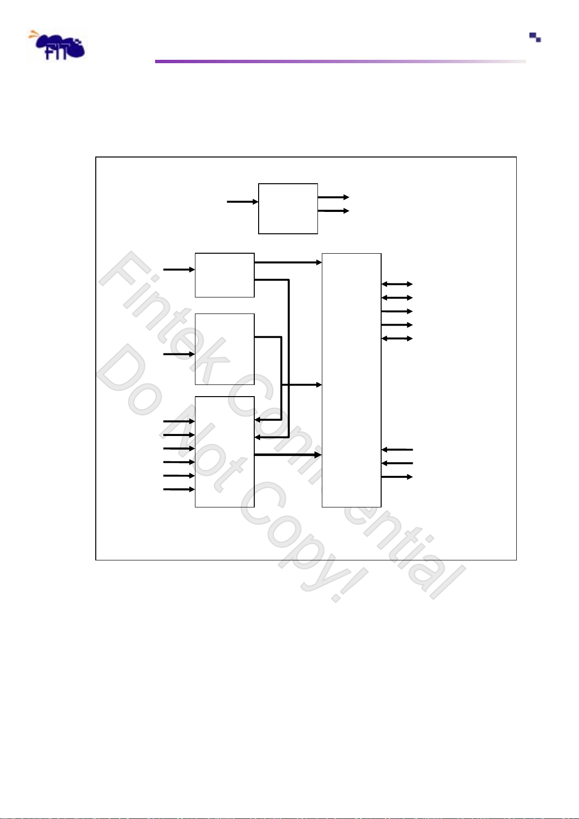
4. Block Diagram
14.318M
3.3V
PWRDN#
Power
Supply
Signal
Power
Down
Control
CLK
GEN./BUF
.
14MOUT1
14MOUT2
ISA
Interface
SA [19:0]
SD [15:0]
AEN
BALE
IOCHRDY
…………………
PCIRST#
LFRAM#
LDRQ#
PCICLK
SERIRQ
LAD [3:0]
LPC
Interface
IRQ [3:7,9:12,14,15]
DRQ [0:3,5:7]
DACK [0:3,5:7]
F85226F
2
Page 8
k
F
Finte
Feature Integration Technology Inc.
F85226
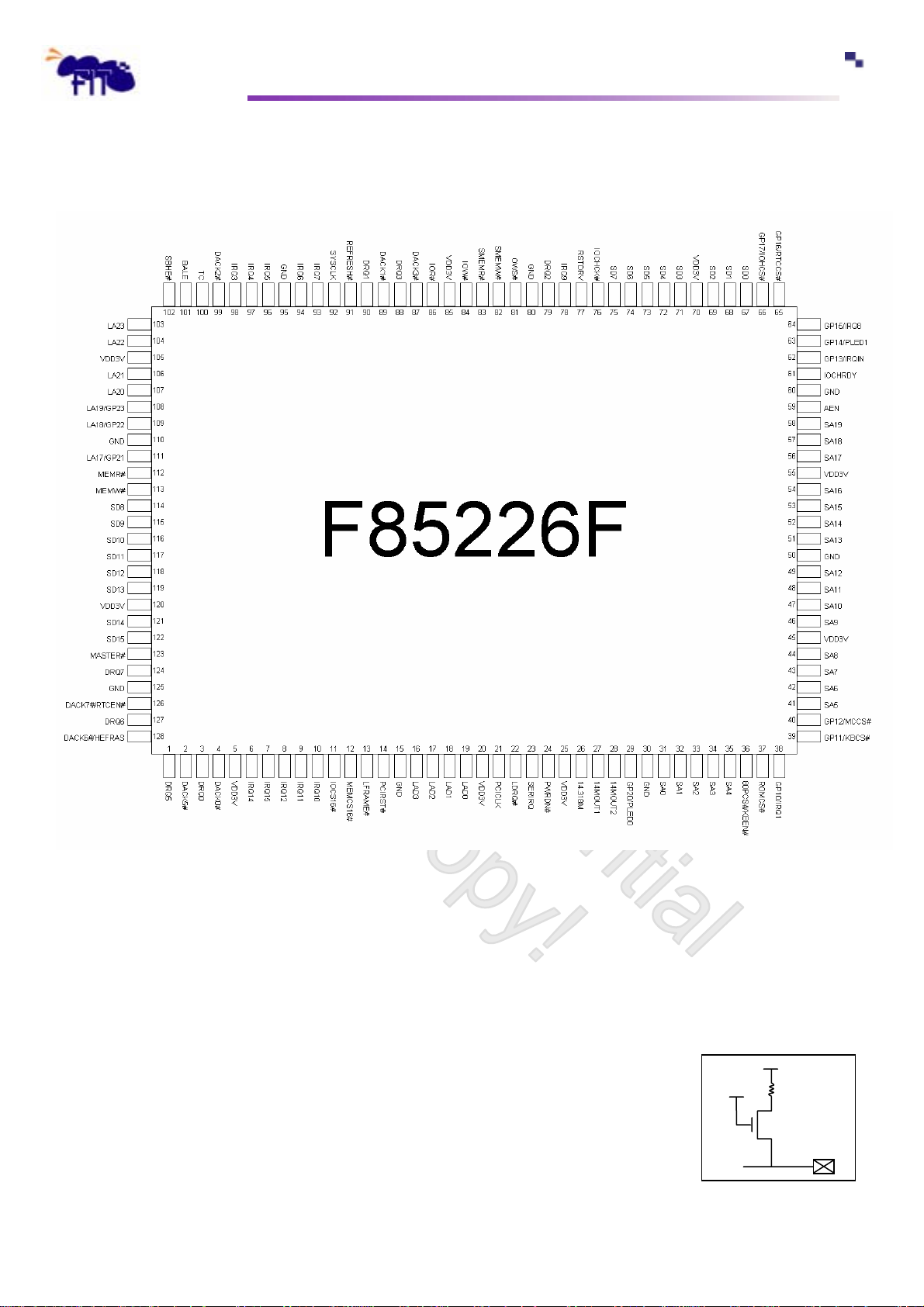
5. Pin Configuration
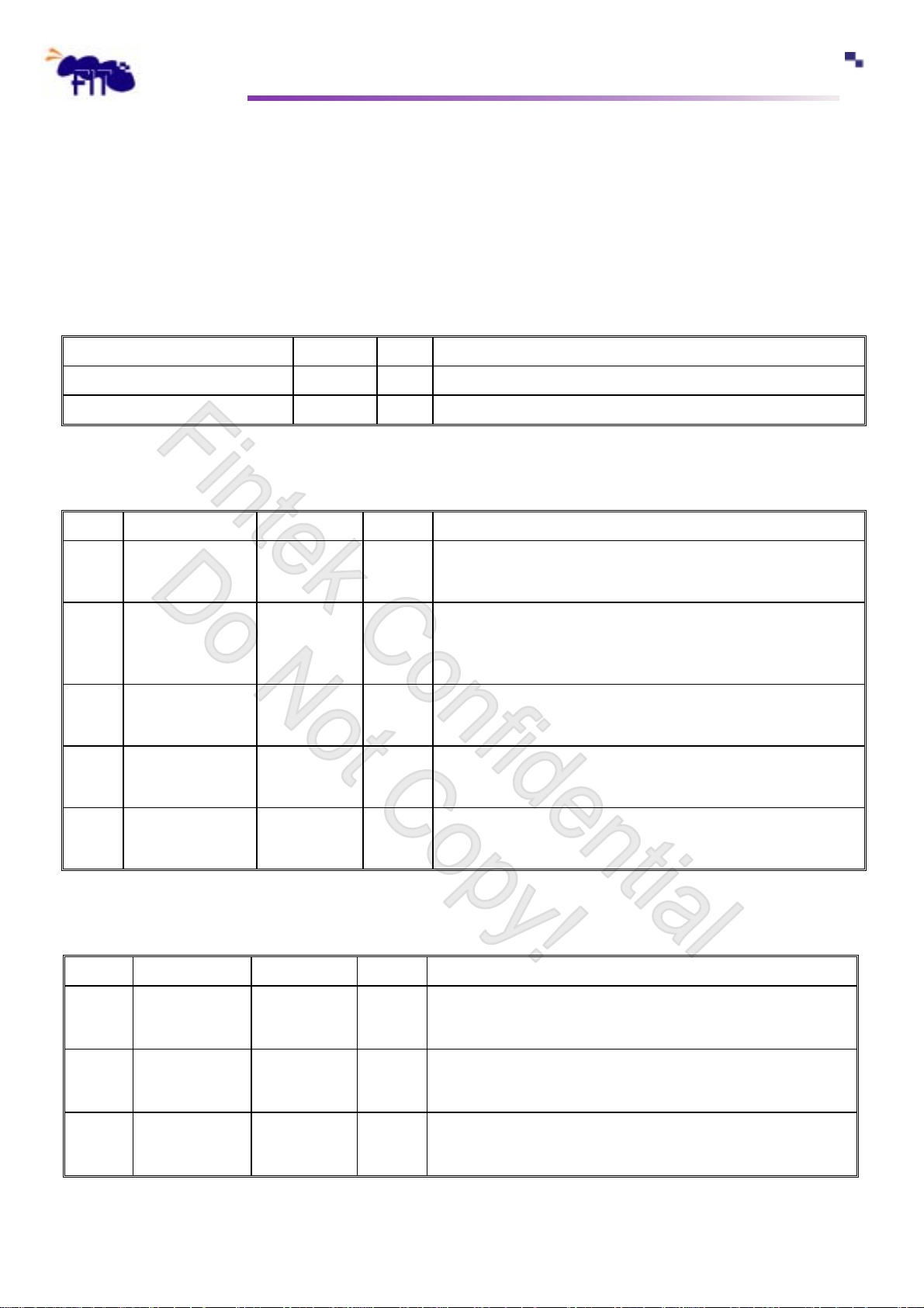
6. Pin Descriptions
I/O
- TTL level bi-directional pin and Schmitt trigger with 24 mA source-sink capability.
24ts
I/OD
24ts_u100k
I/O
24ts_u100k
O
24_u100k
O
- Output pin with 24 mA source-sink capability.
24
O
- Output pin with 20 mA source-sink capability.
20
F85226F
- TTL level input pin and Schmitt trigger, Open-drain output with 24 mA sink capability, internal pull-up
100KΩ connected with 3.3V to protect electric leakage.
- TTL level input pin and Schmitt trigger, Output pin with 24 mA sink capability, internal pull-up 100KΩ
connected with 3.3V to protect electric leakage.
- Output pin with 24 mA source-sink capability, internal pull-up 100KΩ
connected with 3.3V to protect electric leakage.
3
3.3V
100K
Page 9
k
F
Finte
Feature Integration Technology Inc.
F85226
IN
- TTL level input pin.
t
IN
- TTL level input pin and schmitt trigger.
ts
P - Power.
6.1 Power Pin
Pin No. Pin Name Type Description
5, 20, 25, 45, 55, 70, 85, 105, 120 VDD3V P Standard Power Supply Voltage Input with 3.3V.
15, 30, 50, 60, 80, 95, 110, 125 GND P Ground.
6.2 Power on strapping signal
Pin No Pin Name Ty pe PWR Description
36 80PCS#/KBEN#
37
126 DACK7#/RTCEN#
128 DACK6#/HEFRAS
2 DACK5#/EN_GP2X
ROMCS#/ROM_EN
I/OD
24ts_u100k
(5V-tolerance)
I/O
24ts
(5V-tolerance)
I/O
24ts_u100k
(5V-tolerance)
I/O
24ts_u100k
(5V-tolerance)
I/O
24ts_u100k
(5V-tolerance)
VDD3v
VDD3v
VDD3v
VDD3v
VDD3v
Power-on strapping with external pulled-down resistor 10k will
enable K/B and mouse functions. When it is set, pin 38, 39 and 40
will execute IRQ1, KBCS# and MCCS# signals.
Power-on strapping without internal resister, need external
pulled-up resistor to enable CR03h (BIOS_ROM_EN bit) If there is
a boot-ROM (BIOS). Else if without boot-ROM, please use external
pulled-down 10K resister to disable this BIOS_ROM_EN.
Power-on strapping with external pulled-down 10k resistor will
enable RTC functions. When it is set, pin 64 and 65 will do IRQ8
and RTCCS# signals.
Set this function will change the port that is used to access
configuration registers. Default setting is 4Eh, but by power-on
strapping with a external pulled-down 10k resister change to 2Eh.
Power-on strapping with external pulled-down 10k resistor. Then it
will disable LA [19:17] function and pin108~pin111, pin29 use as
GPIO2X function.
6.3 LPC interface
Pin No. Pin Name Type PWR Description
16-19 LAD[3:0]
13 LFRAME#
21 PCICLK
I/O
IN
IN
24ts
ts
t
VDD3v
VDD3v
VDD3v
F85226F
Multiplexed command, address bi-directional data and cycle status.
Through the LPC bus between a host and a peripheral.
Low pulse indicates start of a new cycle or termination of broken
cycle.
PCI clock used for the LPC bus. Same 33MHz clock as PCI clock
on the host. Same clock phase with typical PCI skew.
4
Page 10

k
F
Finte
14 PCIRST#
23 SERIRQ I/O
22 LDRQ# O24
24
6.4 ISA interface
Pin No. Pin Name Type PWR Description
58-56
PWRDN#
SA[19:17]
I/O
24ts_u100k
(5V-tolerance)
IN
IN
ts
24ts
ts
VDD3v
VDD3v
VDD3v
VDD3v
VDD3v
PCI system reset used for the LPC bus. The Reset signal line can
be connected to PCIRST# signal on the host.
Serial IRQ Input/Output.
Encoded DMA Request signal.
Power Down. The signal is active low according to CR 44 Bit 7and
wake-up enable by hardware setting. There are eight different
power-down states (Power down Mode 3).
System Address Bus. These are the upper addresses that define
the ISA’s byte address space (up to 1 M byte). The SA [19:17] are
at tri-states during PCIRST#.
Feature Integration Technology Inc.
F85226
54-51
49-46
44-41
35-31
122-121
119-114
75-71
69-67
59 AEN
86 IOR#
84 IOW#
61 IOCHRDY
92 SYSCLK O24 VDD3v
SA[16:0]
SD[15:0]
I/O
24ts_u100k
(5V-tolerance)
I/O
24ts_u100k
(5V-tolerance)
O
24
(5V-tolerance)
I/O
24ts_u100k
(5V-tolerance)
I/O
24ts_u100k
(5V-tolerance)
I/O
24ts
(5V-tolerance)
VDD3v
VDD3v
VDD3v
VDD3v
VDD3v
VDD3v
System Address Bus. These define the ISA’s byte address space
(up to 128K byte). The SD [16:0] are at tri-states during PCIRST#.
System Data Bus. These provide 16-bit data for devices to reside
on the ISA Bus. The SD [15:0] are at tri-states during PCIRST#.
Address Enable. AEN is asserted during DMA cycles, driven high
during F85226F initiated refresh cycles, driven low upon
PCIRST#.
I/O Read. IOR# is asserted to request an ISA I/O slave to drive
data onto the data bus.
I/O Write. IOW# is asserted to request an ISA I/O slave to accept
data from the data bus.
I/O Channel Ready. IOCHDRY asserted indicates that an ISA
slave requires additional wait states. When the F85226F is an ISA
slave, IOCHRDY is an output indicating additional wait states are
required.
ISA System Clock. SYSCLK offers the reference clock to the ISA
bus. The frequency is generated from dividing PCICLK by 3 or 4
(select by CR06 bit7).
77 RSTDRV O
24
VDD3v
F85226F
Reset Drive. RSTDRV asserted indicates to reset devices that
reside on the ISA Bus while the PCIRST# has been asserted.
5
Page 11

k
F
Finte
11 IOCS16#
12 MEMCS16#
76 IOCHCK#
81 OWS#
103-104
106-107
108-109
111
LA[23:20]
LA[19:17]
GP23, GP22,
GP21
I/O
24ts
(5V-tolerance)
I/O
24ts
(5V-tolerance)
IN
ts
(5V-tolerance)
IN
ts
(5V-tolerance)
I/O
24ts_u100k
(5V-tolerance)
I/O
24ts_u100k
(5V-tolerance)
VDD3v
VDD3v
VDD3v
VDD3v
VDD3v
VDD3v
16-bit I/O Chip Select. IOCS16# is asserted by 16-bit ISA I/O
devices to indicate that they support 16-bit I/O bus cycles.
Memory Chip Select 16. MEMCS16# is asserted by 16-bit ISA
memory devices to indicate that the memory slave supports 16-bit
accesses.
I/O Channel Check. Asserted by an ISA device indicating an error
condition.
Zero Wait States. An ISA slave asserts ZEROWS# after its
address and command signals have been decoded to indicate
that the current cycle can be executed as an ISA zero wait state
cycle. ZEROWS# has no effect during 16-bit I/O cycles.
Unlatched Address. The LA [23:20] address lines are
bi-directional. These address lines allow accesses to physical
memory on the ISA Bus up to 16 Mbytes. LA [23:20] are outputs
when the F85226F owns the ISA Bus.
Unlatched Address. The LA [19:17] address lines are
bi-directional. These address lines allow accesses to physical
memory on the ISA Bus up to 16 Mbytes. LA [19:17] are outputs
when the F85226F owns the ISA Bus.
General purpose I/O pin.
Feature Integration Technology Inc.
F85226
82 SMEMW#
83 SMEMR#
91 REFRESH#
101 BALE
102 SBHE#
112 MEMR#
113 MEMW#
O
24
(5V-tolerance)
O
24
(5V-tolerance)
O
24_u100k
(5V-tolerance)
I/O
24ts_u100k
(5V-tolerance)
I/O
24ts_u100k
(5V-tolerance)
I/O
24ts_u100k
(5V-tolerance)
I/O
24ts_u100k
(5V-tolerance)
VDD3v
VDD3v
VDD3v
VDD3v
VDD3v
VDD3v
VDD3v
Standard (system) Memory Write. SMEMW# is asserted for
memory write accesses below 1MB.
Standard (system) Memory Read. SMEMR# is asserted for
memory read accesses below 1 MB.
Refresh Cycle indicator. REFRESH# asserted indicates that a
refresh cycle is in progress, or ISA master requests F85226F to
generate a refresh cycle. The signal is at tri-stated upon
PCIRST#.
Bus Address Latch Enable. BALE asserted indicates when the
address (SA[19:0], LA[23:17]) and SBHE# are valid. The LA
[23:17] address lines are latched on the trailing edge of BALE.
BALE is driven by low upon PCIRST#.
System Byte High Enable. SBHE# asserted indicates that
SD[15:8] will be used to transfer a byte. SBHE# is at an unknown
state upon PCIRST#.
Memory Read. MEMR# asserted indicates the current ISA bus
cycle is a memory read.
Memory Write. MEMW# asserted indicates the current ISA bus
cycle is a memory write.
F85226F
6
Page 12

k
F
Finte
123 MASTER#
98 IRQ3
97 IRQ4
96 IRQ5
94 IRQ6
93 IRQ7
78 IRQ9
IN
ts
(5V-tolerance)
IN
ts
(5V-tolerance)
IN
ts
(5V-tolerance)
IN
ts
(5V-tolerance)
IN
ts
(5V-tolerance)
IN
ts
(5V-tolerance)
IN
ts
(5V-tolerance)
The MASTER# input asserted indicates an ISA bus master is
VDD3v
VDD3v Parallel Interrupt Requested Input 3.
VDD3v Parallel Interrupt Requested Input 4.
VDD3v Parallel Interrupt Requested Input 5.
VDD3v Parallel Interrupt Requested Input 6.
VDD3v Parallel Interrupt Requested Input 7.
VDD3v Parallel Interrupt Requested Input 9.
driving the ISA bus. This signal is executed with DREQ line by an
ISA master to gain control of the ISA Bus.
Feature Integration Technology Inc.
F85226
10 IRQ10
9 IRQ11
8 IRQ12
6 IRQ14
7 IRQ15
3 DRQ0
90 DRQ1
79 DRQ2
IN
ts
(5V-tolerance)
IN
ts
(5V-tolerance)
IN
ts
(5V-tolerance)
IN
ts
(5V-tolerance)
IN
ts
(5V-tolerance)
IN
ts
(5V-tolerance)
IN
ts
(5V-tolerance)
IN
ts
(5V-tolerance)
VDD3v Parallel Interrupt Requested Input 10.
VDD3v Parallel Interrupt Requested Input 11.
VDD3v Parallel Interrupt Requested Input 12.
VDD3v Parallel Interrupt Requested Input 14.
VDD3v Parallel Interrupt Requested Input 15.
DMA Request input 0. The DREQ asserted indicates that either a
VDD3v
VDD3v DMA Request input 1.
VDD3v DMA Request input 2.
slave DMA device is requesting DMA services or an ISA bus
master is requesting to use the ISA bus.
IN
88 DRQ3
1 DRQ5
F85226F
ts
(5V-tolerance)
IN
ts
(5V-tolerance)
VDD3v DMA Request input 3.
VDD3v DMA Request input 5.
7
Page 13

k
F
Finte
127 DRQ6
124 DRQ7
4 DACK0#
89 DACK1#
99 DACK2#
87 DACK3#
IN
ts
(5V-tolerance)
IN
ts
(5V-tolerance)
O
24
(5V-tolerance)
O
24
(5V-tolerance)
O
24
(5V-tolerance)
O
24
(5V-tolerance)
VDD3v DMA Request input 6.
VDD3v DMA Request input 7.
DMA Acknowledge channel 0. The DACK# outputs asserted
VDD3v
VDD3v DMA Acknowledge channel 1.
VDD3v DMA Acknowledge channel 2.
VDD3v DMA Acknowledge channel 3.
indicates that either a DMA channel or an ISA bus master has
been granted the ISA bus.
Feature Integration Technology Inc.
F85226
DACK5# DMA Acknowledge channel 5.
2
EN_GP2X
DACK6# DMA Acknowledge channel 6.
128
HERFRA
DACK7# DMA Acknowledge channel 7.
126
RTCEN#
100 TC
80PCS#
36
KBEN#
I/O
24ts_u100k
(5V-tolerance)
I/O
24ts_u100k
(5V-tolerance)
I/O
24ts_u100k
(5V-tolerance)
O
24
(5V-tolerance)
I/OD
24ts_u100k
(5V-tolerance)
VDD3v
VDD3v
VDD3v
VDD3v
VDD3v
During power-on strapping with external pulled-down 10k resistor.
Then it will disable LA [19:17] function and pin108~pin111, pin29
use as GPIO2X function.
During power-on reset, this pin is pulled-up internally(Select
4Eh) ,and is defined as HEFRAS which provides the power-on
value for CR3 bit4 .A 10k ohm is recommended if intends to pull
down .(Select 2Eh)
RTC Function Enable. The pin applies a pull-down resistor (4.7K
ohm) to enable RTC functions (RTCCS#, and IRQ8)
Terminal Count. TC signals the final data transfer of a DMA
transfer.
80h PORT Chip Select.(Default)
Only decode IO address port 80h and must apply with IOW#.
K/B Functions Enable. During power-on reset this pin is weak
pulled-up internally. The pin applied a pull-down resistor (10K
ohm) to enable K/B functions. (IRQ1,KBCS#,and MCCS#)
I/O
37
ROMCS#
24ts
(5V-tolerance)
VDD3v
F85226F
ROMCS#, this pin enable positive decoder of BIOS address
range.
8
Page 14

k
F
Finte
ROM_EN
GPIO0 General purpose I/O pin 0.
38
IRQ1
GPIO1 General purpose I/O pin 1.
39
KBCS#
GPIO2 General purpose I/O pin 2.
40
MCCS#
I/O
24ts
(5V-tolerance)
I/O
24t
(5V-tolerance)
I/O
24ts
(5V-tolerance)
VDD3v
VDD3v
VDD3v
Power-on strapping with internal pulled-up resistor will enable
CR03h (BIOS_ROM_EN, BIOS_WR_EN bit). If there is a
boot-ROM (BIOS), else if without boot-ROM, please use external
pulled-down 10K resister to disable this ROM_EN and WR_EN.
Parallel Interrupt Requested Input 1. This pin is used for specific
K/B functions.
Decode address 60h and 64h to generate chip selected signal.
Enable by KBEN# power-on setting.
Decode address 62h and 66h to generate chip selected signal.
Enable by KBEN# power-on setting.
Feature Integration Technology Inc.
F85226
GPIO3 General purpose I/O pin 3.
62
IRQIN
GPIO4 General purpose I/O pin 4.
63
PLED
GPIO5 General purpose I/O pin 5.
64
IRQ8
GPIO6 General purpose I/O pin 6.
65
RTCCS#
GPIO7 General purpose I/O pin 7.
66
IOHCS#
26 14.318M
I/O
24ts
(5V-tolerance)
I/O
24ts
(5V-tolerance)
I/O
24ts
(5V-tolerance)
I/O
24ts
(5V-tolerance)
I/O
24ts
(5V-tolerance)
IN
ts
(5V-tolerance)
VDD3v
VDD3v
VDD3v
VDD3v
VDD3v
VDD3v 14.318 MHz Clock Input.
It is programmable to transfer parallel IRQ input to serial IRQ,
Enable by KBEN# power-on setting.
Power LED output, the signal is at low state after system reset.
Parallel Interrupt Requested Input 8. This interrupt request is used
for specific RTC functions. Enable by RTCEN# power-on setting.
Decode address 70h and 71h to generate chip selected signal.
Enable by RTCEN# power-on setting.
Decode SA [15-11] all are at “0” state initially and setting by CR04
Bit 6.
O
27 14MOUT 1
28 14MOUT 2
GP20 General purpose I/O pin.
29
PLED
F85226F
20
O
20
I/O
24ts
(5V-tolerance)
VDD3v 14.318 MHz Buffer Output 1.
VDD3v 14.318 MHz Buffer Output 2.
VDD3v
Power LED output, the signal is at low state after system reset.
9
Page 15

k
F
Finte
Feature Integration Technology Inc.
F85226
7. Function Description
7.1 LPC interface:
The F85226F implemented full functions that described in the LPC I/F 1.1 specification and transfers
all subtractive cycles from LPC bus to ISA interface for more ISA compatibility. The F85226F built in 16-bit
IO/ Memory enhances transaction. Peripheral or Master devices can assert cycles that are not defined in
positive decode ranges of LPC Interface. All LPC bus signals use PCI electrical characteristics. The
following cycle types are supported by F85226F.
z IO read write (8 / 16 bit)
z Memory read write (8 / 16 bit)
z DMA read write (8/ 16 / 32 bit)
z Firmware memory read write (only support size 8 or 16 bit).
eCycles:
S: Start Cycle
C: Command Type Cycle
Cycle Types Encoding Remark
IO Read
IO Write
Memory Read
Memory Write
DMA Read
DMA Write
Booting Memory Read
Booting Memory Write S: 0xEh; Size: 8, 16, and 32 bit, for LPC peripheral.
S: 0x0h;
C: 0x0h
S: 0x0h;
C: 0x2h
S: 0x0h;
C: 0x4h
S: 0x0h;
C: 0x6h
S: 0x0h;
C: 0x8h
S: 0x0h;
C: 0xAh
S: 0xDh;
Size: 8 bit and 16 bit in Enhanced mode, for LPC peripheral.
Size: 8 bit and 16 bit in Enhanced mode, for LPC peripheral.
Size: 8 bit and 16 bit in Enhanced mode, for LPC peripheral and host.
Size: 8 bit and 16 bit in Enhanced mode, for LPC peripheral and host.
Size: 8, 16 and 32 bit, for LPC peripheral.
Size: 8, 16 and 32 bit, for LPC peripheral.
Size: 8, 16, 32 and 1024 bit, for LPC peripheral.
Start:
The cycle indicates the beginning or abort of a transaction. When LFRAME# is asserted low and monitors
LAD[3:0] that determine frame type to enter a valid Start.
Cycle Type and Direction:
LPC host will issue the transaction cycle and direction by LAD[3:1] and LAD0 is always ignored.
F85226F
10
Page 16

k
F
Finte
Feature Integration Technology Inc.
F85226
Size:
LPC host on DMA or bus master on memory transaction issue data size that will be transferred by LAD[1:0]
and LAD[3:2] must be driven 0x00b.
Turn-Around:
LPC host or peripheral will issue two clock wide cycles after turning control over to peripheral or turning
back from peripheral to host. LAD[3:0] should be driven to high level on first cycle and release to tri-state
on next one.
Address:
While doing IO transaction, this duration is four clock wide that indicates 16-bit address, on Memory cycles
there are eight clocks that indicates 32-bit address will be asserted by LPC host or Master. The duration is
not asserted on DMA transaction.
Channel and Terminal count:
Only on DMA transferring, LAD[2:0] signals indicate granted channel in one clock cycle. LAD[3] indicates
Terminal count down.
Data:
Each frame can carry one byte (8 bit), first nibble is Data[7;4] and next is Data[3:0].
SYNC:
LPC host or peripheral can add wait state, response error and ready to accept a frame by LAD[3:0].
0x0h: Ready
0x5h: Short Wait, maximum number of SYNC is 8 clocks.
0x6h: Long Wait, no maximum number.
0x9h: Ready More on DMA transaction.
0xAh: Error, it relates to IOCHK# on ISA interface.
Others: Reserved.
STA : .. Start Cycle
CT : .. Cycle Type and Direction
H_TAR: . Host Turn-Around
P_TAR: Peripheral Turn-Around
LCLK
LFRAME#
LAD[3:0]
Figure: Read Cycles
STA
CT Addr[15:0]/ [31:0]
F85226F
H_TAR
11
SYNCSYNCSYNC
Data[7:0]Data[7:0]
P_TAR
Page 17

k
F
Finte
LCL
LFRAME#
LAD[3:0]
Figure: Write Cycles
7.1.1 IO/Memory Read and Write Cycles
When LPC interface Bridge issues IO cycles that meet subtractive decode, F85226F will assert
corresponded IOR#, IOW# , MEMR# ,SMEMR# , MEMW# and SMEMW# then respond by inserting wait
cycles (long wait SYNC). After finishing ISA transaction and there isn’t any valid ISA Wait state inserted, it
responds Ready-state and terminates the cycles. If the host issues 16 bit transfer, F85226F will active
enhance 16-bit transferring function automatically.
STA
CT Addr[15:0]/ [31:0]
Data[7:0]Data[7:0]
Feature Integration Technology Inc.
F85226
H_TAR
SYNCSYNCSYNC
P_TAR
7.1.2 DMA Read and Write Cycles
The read transactions transfer data from main memory to peripheral and write cycles transfer data
from peripheral to main memory. DMA requests form ISA interface are delivered by LDRQ# to DMA
controller (like 8237) and the acknowledge responds from LAD [3:0] encoding message. Terminal count is
depended on the counter programmed in DMA controller, when reach the counter threshold, TC is related
to LAD3 and asserted when DMA controller plan to terminal DMA transaction.
7.1.3 Booting Memory Read and Write Cycles
The ISA interface of F85226F can communicate to ISA ROM (System BIOS) with ROMCS#, MEMER#
and MEMW#, BIOS booting cycles of PC system may assert through different cycle type ( like Memory
Read and Firmware Memory Read) , F85226F can perform a positive decoder on specified memory range
included legacy BIOS , extended legacy BIOS and user defined High Memory address.
F85226F
12
Page 18

k
F
Finte
0xFFFFFFFFh
0xFFE00000h
Feature Integration Technology Inc.
F85226
ROMCS#
0x000FFFFFh
0x000F0000h
0x000E0000h
Legacy BIOS
Extended BIOS
0x00000000h
Figure: Chip Select of BIOS Memory
7.2 Serialized Interrupt
Serial Interrupt is a single bus that transmits parallel legacy interrupts and encodes suitable packet at
corresponded moment. The signal refers to LCLK and it operates on an open-drain bus (multi-drop bus)
that is shared with other devices. F85226F supports two operation types included Continuous and Quiet
mode. Eventually, it fully meets SERIRQ specification Version 6.0.
R: Recovery Phase, SERIRQ signal is driven to high level
T: Turn-Around Phase, Devices Tri-state SERIRQ,
S: Sampling Phase, SERIRQ signal is sink to low level
RTS RTSRT
LCLK
SERIRQ
START
STOPIRQx
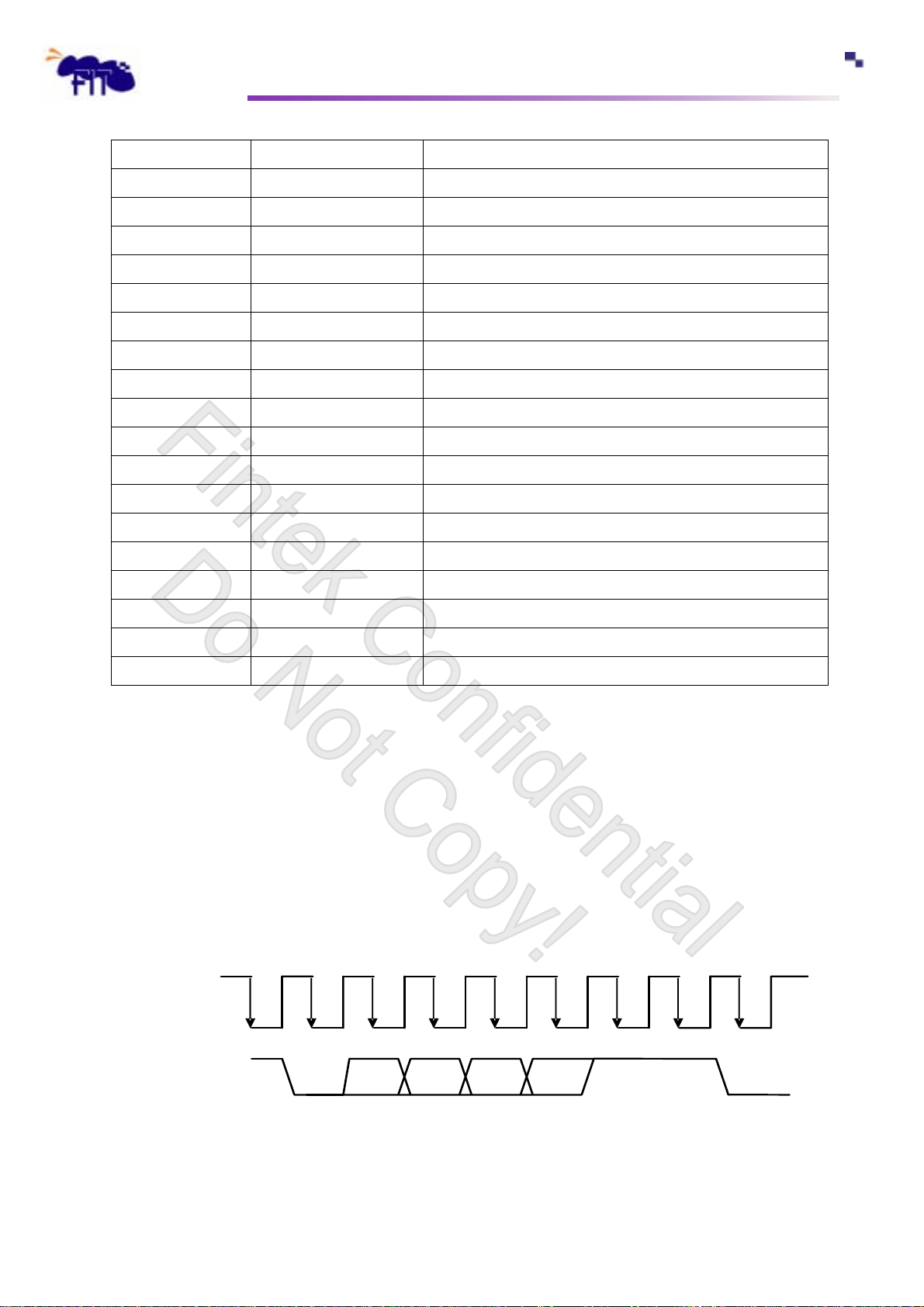
To identify parallel IRQ type on SERIRQ, following the table list supported source.
One SERIRQ Field contains three states included Recovery, Turn-Around and Sample.
F85226F
13
Page 19
k
F
Finte
SERIRQ Field Parallel IRQ Number of clocks after Start finished (Rising Edge)
1 Reserved 2
2 Reserved 5
3 Reserved 8
4 IRQ3 11
5 IRQ4 14
6 IRQ5 17
7 IRQ6 20
8 IRQ7 23
9 Reserved 26
10 IRQ9 29
11 IRQ10 32
12 IRQ11 35
13 IRQ12 38
Feature Integration Technology Inc.
F85226
14 Reserved 41
15 IRQ14 44
16 IRQ15 47
17 IOCHK# 50
21:18 Reserved 53, 56, 59 , 62
Table: SERIRQ map
7.3 LPC DMA
LPC DMA supports Signal, Demand, Verify and Increment operations. The DMA channels are
compatible with ISA interface. All channels can be encoded to LDRQ# in serial format even channel 4 that
requests a bus master to LPC host. Channels 0-3 are for 8-bit transaction and channel 5-7 are for 16-bit
transaction. F85226F also supports 32-bit DMA if LPC host issues. LDRQ# also refers to LCLK and
samples in negative edge by LPC host. ACT field indicates the DMA aborts or not.
LCLK
LDRQ#
START
Figure: LCLK and LDRQ#
F85226F
MSB LSB ACT
START
14
Page 20

k
F
Finte
Feature Integration Technology Inc.
F85226
8. Registers Description
8.1 Entry Key: Write 26h to the location 4Eh ( Default ) twice will enable the following
configuration registers. Change the location to 2Eh by power-on strapping with an external
pulled-down resister on pin 128.
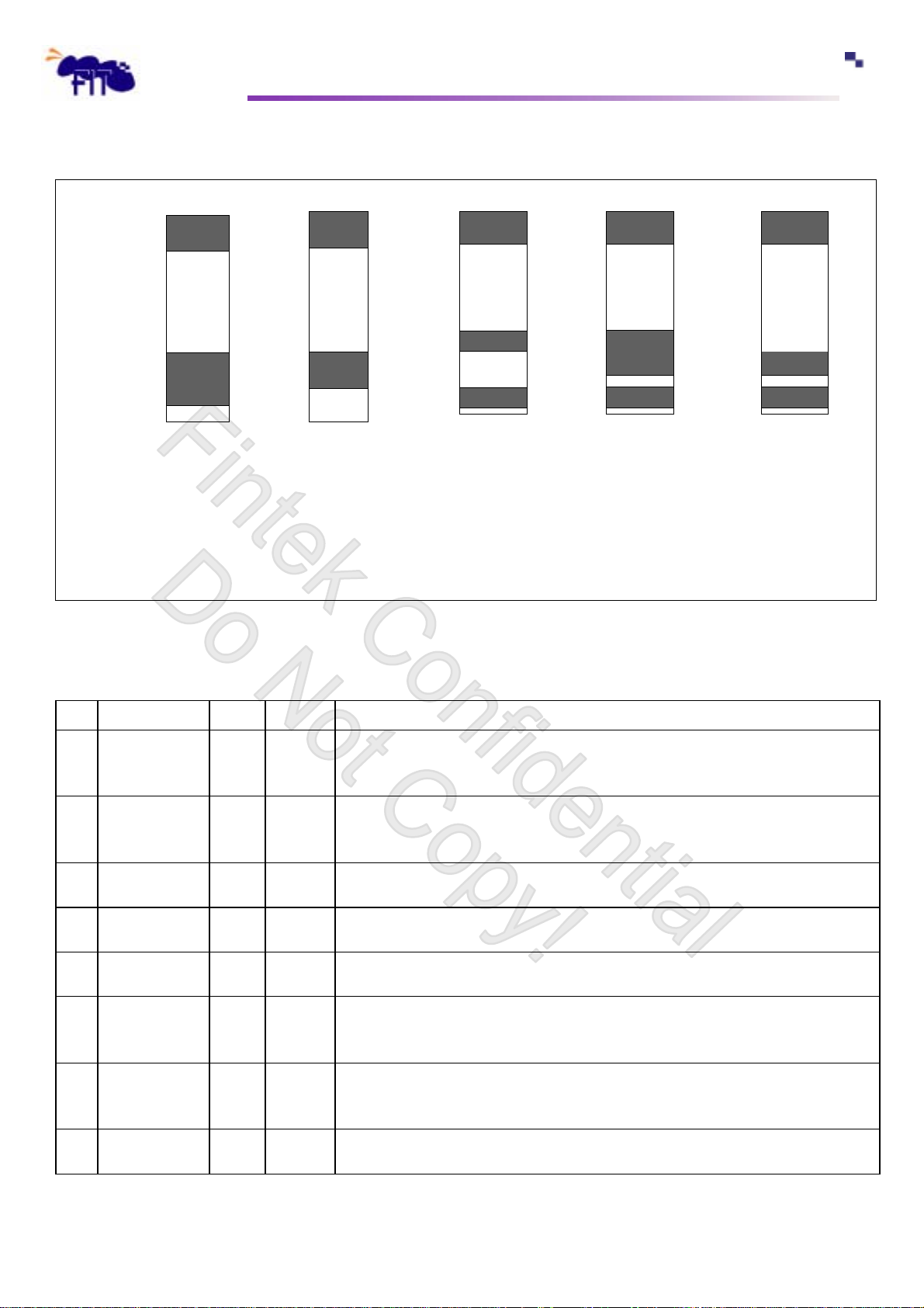
8.2 Configuration and Control Register – Index 03h
Power-on default [7:0] =00_100_0_s_0b (s: mean default value effect by strapping)
Bit Name R/W PWR Description
7-6 ROM_SEL_TYPE R/W VDD3V 00: ROMCS# decoder address 0xF_xxxx, and 0xE_xxxx if BIOS_0E_EN set to 1
(REG03h bit0).
01: ROMCS# decoder address by define address 1 (REG2Ah, 2Bh) and define
address 2 (REG 2Eh, 2Fh).
10: ROMCS# decoder address 0xF_xxxx, and 0xE_xxxx if BIOS_0E_EN set to 1
(REG03h bit0) or ROMCS# decoder address by define address 1 (REG2Ah,
2Bh) and define address 2 (REG 2Eh, 2Fh).
11: ROMCS# decoder address 0xF_xxxx, and 0xE_xxxx if BIOS_0E_EN set to 1
(REG03h bit0) or ROMCS# decoder address by define address 1 (REG2Ah,
2Bh) and define address 2 (REG 2Eh, 2Fh).
4-2 BIOS_ROM_SIZE R/W VDD3V 000: ROMCS# decodes range 1M.
001: ROMCS# decodes range 2M.
010: ROMCS# decodes range 4M.
011: ROMCS# decodes range 8M.
100: ROMCS# decodes range 16M.
101: ROMCS# decodes range 32M.
110: ROMCS# decodes range 64M.
111: ROMCS# decodes range 1M.
2 BIOS_0E_EN R/W VDD3V Enable ROMCS# to decode the address 0xE_XXXX.
1 BIOS_ROM_EN R/W VDD3V Enable ROMCS# to decode address.
0 BIOS_WR_EN R/W VDD3V When BIOS_ROM_EN is enabled, sets this bit to protect BIOS write.
F85226F
15
Page 21
k
F
Finte
Feature Integration Technology Inc.
F85226
0xFFFF_FFFF
0xFFFF_0000
0x000F_FFFF
0x000E_0000
BIOS_OE_EN = 1
ROM_SEL_TYPE =0
0xFFFF_FFFF
0xFFFF_0000
0x000F_FFFF
0x000F_0000
BIOS_OE_EN = 0
ROM_SEL_TYPE =0
BIOS_ROM_SIEZ = 00
0xFFFF_FFFF
0xFFFF_0000
0x000F_FFFF
0x000F_F000
0x000C_FFFF
0x000C_F000
BIOS_OE_EN = 1,
ROM_SEL_TYPE =1
REG 2Bh = 0xFF,
REG 2Ah = 0xFF
REG 29h = 0x00,
REG 28h = 0xFF
REG 2Fh = 0xCF,
REG 2Eh = 0xFF
REG 2Dh = 0x00,
REG 2Ch = 0xFF
0xFFFF_FFFF
0xFFFF_0000
0x000F_FFFF
0x000E_0000
0x000C_FFFF
0x000C_F000
0xFFFF_FFFF
0xFFFF_0000
0x000F_EFFF
0x000E_0000
0x000C_FFFF
0x000C_F000
BIOS_OE_EN = 1,
ROM_SEL_TYPE =2
REG 2Bh = 0xFF,
REG 2Ah = 0xFF
REG 29h = 0x00,
REG 28h = 0xFF
REG 2Fh = 0xCF,
REG 2Eh = 0xFF
REG 2Dh = 0x00,
REG 2Ch = 0xFF
BIOS_OE_EN = 1,
ROM_SEL_TYPE =3
REG 2Bh = 0xFF,
REG 2Ah = 0xFF
REG 29h = 0x00,
REG 28h = 0xFF
REG 2Fh = 0xCF,
REG 2Eh = 0xFF
REG 2Dh = 0x00,
REG 2Ch = 0xFF
8.3 GPIO1 Function Select Register – Index 04h
Power-on default [7:0] =0ss0_ssssb
Bit Name R/W PWR Description
Set this bit to 0, the pin GP17/IOHCS# will be used as GP17 function. Set to 1, the pin
7 GP17_MODE R/W VDD3V
6 GP16_MODE R/W VDD3V
5 GP15_MODE R/W VDD3V
4 GP14_MODE R/W VDD3V
3 GP13_MODE R/W VDD3V
2 GP12_MODE R/W VDD3V
1 GP11_MODE R/W VDD3V
0 GP10_MODE RO VDD3V
GP17/IOHCS# used as IOHCS# function and decode range can program by (REG
0x3F~0x41).
Set this bit to 0, the pin GP16/RTCCS# will be used as GP16 function. Set to 1, the pin
GP16/RTCCS# used as RTCCS# function and decode range can program by (REG
0x3C~0x3E). The default value is strapping by RTCEN.
Set this bit to 0, the pin GP15/IRQ8 will be used as GP15 function or GPCS#. Set to 1,
the pin GP15/IRQ8 used as IRQ8. The default value is strapping by RTCEN.
Set this bit to 0, the pin GP14/PLED1 will be used as GP14 function. Set to 1, the pin
GP12/PLED1 used as PLED1.
Set this bit to 0, the pin GP13/IRQIN will be used as GP13 function. Set to 1, the pin
GP13/IRQIN used as IRQIN function. The default value is strapping by KBEN
Set this bit to 0, the pin GP12/MCCS# will be used as GP12 function. Set to 1, the pin
GP12/MCCS# used as MCCS# function and decode range can program by (REG
0x39~0x3B). The default value is strapping by KBEN
Set this bit to 0, the pin GP11/KBCS# will be used as GP11 function. Set to 1, the pin
GP11/KBCS# used as KBCS# function and decode range can program by (REG
0x36~0x38). The default value is strapping by KBEN
Set this bit to 0, the pin GP10/IRQ1 will be used as GP10 function or GPCS#. Set to 1,
the pin GP10/IRQ1 used as IRQ1. The default value is strapping by KBEN.
F85226F
16
Page 22

k
F
Finte
Feature Integration Technology Inc.
F85226
8.4 GPIO2 Function Select Register – Index 05h
Power-on default [7:0] =0000_sss0b
Bit Name R/W PWR Description
7-5 Reserved RO VDD3V
3 GP23_MODE R/W VDD3V
2 GP22_MODE R/W VDD3V
1 GP21_MODE R/W VDD3V
0 GP20_MODE R/W VDD3V
Set this bit to 0, the pin SA19/GP23 will be used as GP23 function or GPCS#. Set to 1,
the pin SA19/GP23 used as SA19. The default value is strapping by DACK5#.
Set this bit to 0, the pin SA18/GP22 will be used as GP22 function or GPCS#. Set to 1,
the pin SA18/GP22 use as SA18. The default value is strapping by DACK5#.
Set this bit to 0, the pin SA17/GP21 will be used as GP21 function or GPCS#. Set to 1,
the pin SA17/GP21 used as SA17. The default value is strapping by DACK5#.
Set this bit to 0, the pin GP20/PLED0 will be used as GP20 function or GPCS#. Set to
1, this pin will be used as PLED0 output.
(When use in LED mode, GP20 output control “CR18” must select to output mode,
and user need to take care that decoder select ”CR13,14” can’t select to pin GP20).
8.5 System Clock Register – Index 06h
Power-on default [7:0] =0000_0000b
Bit Name R/W PWR Description
7 SYSCLK_SEL R/W VDD3V
6 EN_RECOVER8 R/W VDD3V
5-3 RECOVER_TIME8 R/W VDD3V
2 EN_RECOVER16 R/W VDD3V
1-0 RECOVER_TIME16 R/W VDD3V
Set to 1, ISA system clock period will be 3 PCI clock. Set to 0, system clock
period will be 4 PCI clock.
Set to 1, enable bit [5:3] setting. Set to 0, disable bit [5:3] setting and uses 3.5
SYSCLKs for 8 bits I/O recovery time.
When bit 6 was set to 1, these 3 bits field define the additional number of
SYSCLKs added to standard 3.5 SYSCLKs recovery time for 8 bits I/O.
= 000 --- 0 SYSCLK
= 001 --- 1 SYSCLK
= 010 --- 2 SYSCLKs
= 011 --- 3 SYSCLKs
= 100 --- 4 SYSCLKs
= 101 --- 5 SYSCLKs
= 110 --- 6 SYSCLKs
= 111 --- 7 SYSCLKs
Set to 1, enable bit [1:0] setting. Set to 0, disable bit [1:0] setting and uses 3.5
SYSCLKs for 16 bits I/O recovery time.
.When bit 2 was set to 1, these 3 bits field define the additional number of
SYSCLKs added to standard 3.5 SYSCLKs recovery time for 16 bits I/O.
= 01 --- 1 SYSCLK
= 10 --- 2 SYSCLK s
F85226F
17
Page 23
k
F
Finte
= 11 --- 3 SYSCLK s
= 00 --- 4 SYSCLK s
Feature Integration Technology Inc.
F85226
8.6 System Power down Register – Index 10h
Power-on default [7:0] =0011_0000b
Bit Name R/W PWR Description
7 Reserved R/W VDD3V
6 SOFT_DOWN R/W VDD3V Set this bit to isolate ISA bus.
5 EN_CLKOUT_PD R/W VDD3V Enable CLKOUT1 and CLKOUT2 power down when isolate the ISA bus.
4 EN_SYSCLK_PD R/W VDD3V Enable SYSCLK to power down when isolate the ISA bus.
3 EN_REFRESH R/W VDD3V Enable refresh output.
2 DIS_CLKOUT2 R/W VDD3V If this bit set to 1, CLKOUT2 will power down.
1 DIS_CLKOUT1 R/W VDD3V If this bit set to 1, CLKOUT1 will power down.
0 EN_GPIO R/W VDD3V Set this bit to enable write command to REG 0x11~0x1A.
8.7 GPIO Port Define Register (Low byte)– Index 11h
Power-on default [7:0] =0000_0000b
Bit Name R/W PWR Description
7-0 GP_ADDR[7:0] R/W VDD3V
User defines port address to control GPIO functions. To control GPIO state
without entry configure mode. (If GPIO no enable “CR10 bit0”, This register will
read only).
For example: if define GP_ADDR 0x150 in CR11 and CR12t.
If(GPIO output ctrl (REG 0x15, 0x18) set to output mode then:
-o 150 aa (10101010b) to set GP17, GP15, GP13 and GP11 to High.
-o 150 55 (01010101 b) to set GP16, GP14, GP12 and GP10 to High.
-o 151 aa (10101010b) to set GP23 and GP21 to High.
-o 151 55 (01010101 b) to set GP22 and GP20 to High.
If(GPIO output ctrl (REG 0x15, 0x18) set to input mode then:
- i 150 ------show pin states of GP1[7..0].
- i 151------show pin states of GP2[3..0].
F85226F
18
Page 24

k
F
Finte
Feature Integration Technology Inc.
F85226
8.8 GPIO Port Define Register (High byte)– Index 12h
Power-on default [7:0] =0000_0000b
Bit Name R/W PWR Description
7-0 GP_ADDR[15:8] R/W VDD3V
User defines port address to control GPIO functions. To control GPIO state
without entry configure mode. (If GPIO no enable “CR10 bit0”, This register will
read only).
For example: if define GP_ADDR 0x150 in CR11 and CR12t.
If(GPIO output ctrl (REG 0x15, 0x18) set to output mode then:
-o 150 aa (10101010b) to set GP17, GP15, GP13 and GP11 to High.
-o 150 55 (01010101 b) to set GP16, GP14, GP12 and GP10 to High.
-o 151 aa (10101010b) to set GP23 and GP21 to High.
-o 151 55 (01010101 b) to set GP22 and GP20 to High.
If(GPIO output ctrl (REG 0x15, 0x18) set to input mode then:
-i 150 ------ show pin states of GP1[7..0].
-i 151 ------ show pin states of GP2[3..0].
8.9 Address Decoder Register (I) – Index 013h
Pow er-on default [ 7:0] =1111_1111b
Bit Name R/W PWR Description
7-4 DECODER_SEL2 R/W VDD3V
3-0 DECODER_SEL1 R/W VDD3V
Select GPIO pin to be GPCS2# that define decode address by CR21, 22. (If GPIO
no enable “CR10 bit0”, This register will read only).
0000: if decode_sel2 set to 0x0h the GPCS2 will output from pin GP10.
0011: if decode_sel2 set to 0x3h the GPCS2 will output from pin GP13.
0100: if decode_sel2 set to 0x4h the GPCS2 will output from pin GP14.
0101: if decode_sel2 set to 0x5h the GPCS2 will output from pin GP15.
1000: if decode_sel2 set to 0x8h the GPCS2 will output from pin GP20.
1001: if decode_sel2 set to 0x9h the GPCS2 will output from pin GP21.
1010: if decode_sel2 set to 0xAh the GPCS2 will output from pin GP22.
1011: if decode_sel2 set to 0xBh the GPCS2 will output from pin GP23.
Default : disable.
Select GPIO pin to be GPCS2# that define decode address by CR24, 25. (If GPIO
no enable “CR10 bit0”, This register will read only).
0000: if decode_sel1 set to 0x0h the GPCS1 will output from pin GP10.
0011: if decode_sel1 set to 0x3h the GPCS1 will output from pin GP13.
0100: if decode_sel1 set to 0x4h the GPCS1 will output from pin GP14.
0101: if decode_sel1 set to 0x5h the GPCS1 will output from pin GP15.
1000: if decode_sel1 set to 0x8h the GPCS1 will output from pin GP20.
F85226F
19
Page 25
k
F
Finte
1001: if decode_sel1 set to 0x9h the GPCS1 will output from pin GP21.
1010: if decode_sel1 set to 0xAh the GPCS1 will output from pin GP22.
1011: if decode_sel1 set to 0xBh the GPCS1 will output from pin GP23.
default: disable.
Feature Integration Technology Inc.
F85226
8.10 Address Decoder Register (II) – Index 014h
Pow er-on default [ 7:0] =1111_1111b
Bit Name R/W PWR Description
7-4 DECODER_SEL4 R/W VDD3V
3-0 DECODER_SEL3 R/W VDD3V
Select GPIO pin to be GPCS3# that define decode address by CR31, 32. (If GPIO
no enable “CR10 bit0”, This register will read only).
0000: if decode_sel4 set to 0x0h the GPCS4 will output from pin GP10.
0011: if decode_sel4 set to 0x3h the GPCS4 will output from pin GP13.
0100: if decode_sel4 set to 0x4h the GPCS4 will output from pin GP14.
0101: if decode_sel4 set to 0x5h the GPCS4 will output from pin GP15.
1000: if decode_sel4 set to 0x8h the GPCS4 will output from pin GP20.
1001: if decode_sel4 set to 0x9h the GPCS4 will output from pin GP21.
1010: if decode_sel4 set to 0xAh the GPCS4 will output from pin GP22.
1011: if decode_sel4 set to 0xBh the GPCS4 will output from pin GP23.
default: disable.
Select GPIO pin to be GPCS3# that define decode address by CR34, 35. (If GPIO
no enable “CR10 bit0”, This register will read only).
0000: if decode_sel3 set to 0x0h the GPCS3 will output from pin GP10.
0011: if decode_sel3 set to 0x3h the GPCS3 will output from pin GP13.
0100: if decode_sel3 set to 0x4h the GPCS3 will output from pin GP14.
0101: if decode_sel3 set to 0x5h the GPCS3 will output from pin GP15.
1000: if decode_sel3 set to 0x8h the GPCS3 will output from pin GP20.
1001: if decode_sel3 set to 0x9h the GPCS3 will output from pin GP21.
1010: if decode_sel3 set to 0xAh the GPCS3 will output from pin GP22.
1011: if decode_sel3 set to 0xBh the GPCS3 will output from pin GP23.
default: disable.
8.11 GPIO Input Control Register – Index 15h
Power-on default [7:0] =0000_0000b
Bit Name R/W PWR Description
7 GP17_OCTRL
6 GP16_OCTRL
5 GP15_OCTRL
R/W VDD3V
R/W VDD3V
R/W VDD3V
F85226F
GP17 in/out mode select: GP17 is input mode if set to 0. GP17 is output mode if set to 1.
(If GPIO no enable “CR10 bit0”, This register will read only).
GP16 in/out mode select: GP16 is input mode if set to 0. GP16 is output mode if set to 1.
(If GPIO no enable “CR10 bit0”, This register will read only).
GP15 in/out mode select: GP15 is input mode if set to 0. GP15 is output mode if set to 1.
(If GPIO no enable “CR10 bit0”, This register will read only).
20
Page 26
k
F
Finte
4 GP14_OCTRL
3 GP13_OCTRL
2 GP12_OCTRL
1 GP11_OCTRL
0 GP10_OCTRL
R/W VDD3V
R/W VDD3V
R/W VDD3V
R/W VDD3V
R/W VDD3V
GP14 in/out mode select: GP14 is input mode if set to 0. GP14 is output mode if set to 1.
(If GPIO no enable “CR10 bit0”, This register will read only).
GP13 in/out mode select: GP13 is input mode if set to 0. GP13 is output mode if set to 1.
(If GPIO no enable “CR10 bit0”, This register will read only).
GP12 in/out mode select: GP12 is input mode if set to 0. GP12 is output mode if set to 1.
(If GPIO no enable “CR10 bit0”, This register will read only).
GP11 in/out mode select: GP11 is input mode if set to 0. GP11 is output mode if set to 1.
(If GPIO no enable “CR10 bit0”, This register will read only).
GP10 in/out mode select: GP10 is input mode if set to 0. GP10 is output mode if set to 1.
(If GPIO no enable “CR10 bit0”, This register will read only).
Feature Integration Technology Inc.
F85226
8.12 GPIO Output Data Register – Index 16h
Power-on default [7:0] =0000_0000b
Bit Name R/W PWR Description
GP17_DATA
7
GP16_DATA
6
GP15_DATA
5
GP14_DATA
4
GP13_DATA
3
GP12_DATA
2
GP11_DATA
1
GP10_DATA
0
R/W VDD3V
R/W VDD3V
R/W VDD3V
R/W VDD3V
R/W VDD3V
R/W VDD3V
R/W VDD3V
R/W VDD3V
When GP17 in out mode, set this bit to write data to pin GP17. (If GPIO no enable
“CR10 bit0”, This register will read only).
When GP16 in out mode, set this bit to write data to pin GP16. (If GPIO no enable
“CR10 bit0”, This register will read only).
When GP15 in out mode, set this bit to write data to pin GP15. (If GPIO no enable
“CR10 bit0”, This register will read only).
When GP14 in out mode, set this bit to write data to pin GP14. (If GPIO no enable
“CR10 bit0”, This register will read only).
When GP13 in out mode, set this bit to write data to pin GP13. (If GPIO no enable
“CR10 bit0”, This register will read only).
When GP12 in out mode, set this bit to write data to pin GP12. (If GPIO no enable
“CR10 bit0”, This register will read only).
When GP11 in out mode, set this bit to write data to pin GP11. (If GPIO no enable
“CR10 bit0”, This register will read only).
When GP10 in out mode, set this bit to write data to pin GP10. (If GPIO no enable
“CR10 bit0”, This register will read only).
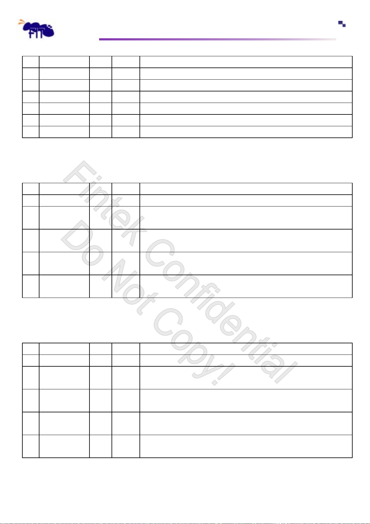
8.13 GPIO1x Input Register – Index 17h
Power-on default [7:0] =pppp_ppppb (p: mean pin status)
Bit Name R/W PWR Description
7 GP17_ST RO VDD3V This bit is read only, when read back is the status of the pin GP17.
F85226F
21
Page 27
k
F
Finte
6 GP16_ST RO VDD3V This bit is read only, when read back is the status of the pin GP16.
5 GP15_ST RO VDD3V This bit is read only, when read back is the status of the pin GP15.
4 GP14_ST RO VDD3V This bit is read only, when read back is the status of the pin GP14.
3 GP13_ST RO VDD3V This bit is read only, when read back is the status of the pin GP13.
2 GP12_ST RO VDD3V This bit is read only, when read back is the status of the pin GP12.
1 GP11_ST RO VDD3V This bit is read only, when read back is the status of the pin GP11.
0 GP10_ST RO VDD3V This bit is read only, when read back is the status of the pin GP10.
8.14 GPIO2 Input Control Register – Index 18h
Feature Integration Technology Inc.
F85226
Power-on default [7:0] =0000_0000b
Bit Name R/W PWR Description
7 Reserved - - Reserved.
3
GP23_OCTRL
R/W VDD3V
GP23 in/out mode select: GP23 is input mode if set to 0. GP23 is output mode if set to 1.
(If GPIO no enable “CR10 bit0”, This register will read only).
GP22_OCTRL
2
GP21_OCTRL
1
GP20_OCTRL
0
R/W VDD3V
R/W VDD3V
R/W VDD3V
GP22 in/out mode select: GP22 is input mode if set to 0. GP22 is output mode if set to 1.
(If GPIO no enable “CR10 bit0”, This register will read only).
GP21 in/out mode select: GP21 is input mode if set to 0. GP21 is output mode if set to 1.
(If GPIO no enable “CR10 bit0”, This register will read only).
GP20 in/out mode select: GP20 is input mode if set to 0. GP20 is output mode if set to 1.
(If GPIO no enable “CR10 bit0”, This register will read only).
8.15 GPIO2 Output Data Register – Index 19h
Power-on default [7:0] =0000_0000b
Bit Name R/W PWR Description
7 Reserved R/W VDD3V Reserved
GP23_DATA
3
GP22_DATA
2
R/W VDD3V
R/W VDD3V
When GP23 in out mode, set this bit to write data to pin GP23. (If GPIO no enable
“CR10 bit0”, This register will read only).
When GP22 in out mode, set this bit to write data to pin GP22. (If GPIO no enable
“CR10 bit0”, This register will read only).
GP21_DATA
1
GP20_DATA
0
R/W VDD3V
R/W VDD3V
F85226F
When GP21 in out mode, set this bit to write data to pin GP21. (If GPIO no enable
“CR10 bit0”, This register will read only).
When GP20 in out mode, set this bit to write data to pin GP20. (If GPIO no enable
“CR10 bit0”, This register will read only).
22
Page 28
k
F
Finte
Feature Integration Technology Inc.
F85226
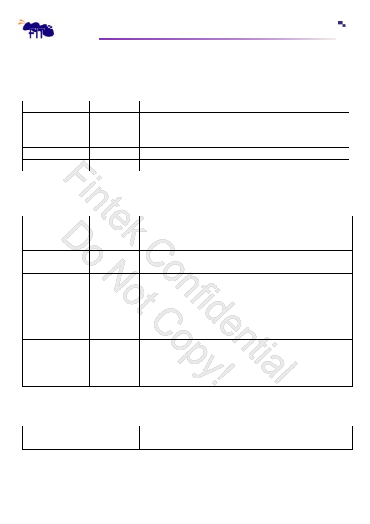
8.16 GPIO2 Input Register – Index 1Ah
Power-on default [7:0] =0000_ppppb (p: mean pin status)
Bit Name R/W PWR Description
7-4 Reserved R/W VDD3V Reserved
3 GP23_ ST R/W VDD3V This bit is read only, when read back is the status of the pin GP23.
2 GP22_ ST R/W VDD3V This bit is read only, when read back is the status of the pin GP22.
1 GP21_ ST R/W VDD3V This bit is read only, when read back is the status of the pin GP21.
0 GP20_ ST R/W VDD3V This bit is read only, when read back is the status of the pin GP20.
8.17 LED & IRQIN Control Register – Index 1Bh
Power-on default [7:0] =0000_0000b
Bit Name R/W PWR Description
7 ADDR_DEC_TY
PE[1]
6 ADDR_DEC_TY
PE[0]
5-4 LED_FREQ R/W VDD3V
3-0 IRQIN_SEL R/W VDD3V
R/W VDD3V
R/W VDD3V
If set to 1, the address decode 4 (CR34, CR35) will decode the memory cycle, else
it will decode io cycle.
If set to 1, the address decode 3 (CR31, CR32) will decode the memory cycle, else
it will decode io cycle.
When pin GP14 or GP20 be selected to LED mode, user can use these two bits to
define LED frequency:
00: Power LED pin is tri-stated.
01: Power LED pin is driven low.
10: Power LED pin is a 1Hz toggle pulse with 50 duty cycle.
11: Power LED pin is a 1/2 Hz toggle pulse with 50 duty cycle.
These bits select IRQ resource for IRQIN. Four bits transfer the decimal value
to octal system.
For example:
Bit [3..0] = 1001b = 0x9h means IRQ 9 be selected.
Bit [3..0] = 1100b = 0xCh means IRQ12 be selected.
8.18 Master Setting Register – Index 1Ch
Power-on default [7:0] =1110_0001b
Bit Name R/W PWR Description
7-0 EN_MASTER16_CH R/W VDD3V Reserved
F85226F
23
Page 29
k
F
Finte
Feature Integration Technology Inc.
F85226
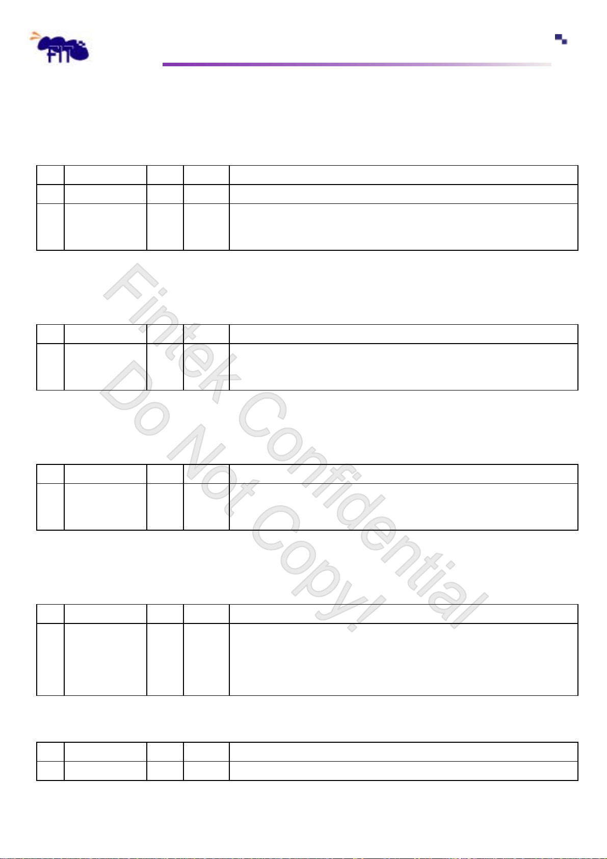
8.19 Master Setting Register – Index 1Dh
Power-on default [7:0] =0110_0011b
Bit Name R/W PWR Description
7 EN_TIMEOUT R/W VDD3V Enable this bit to timeout LPC long wait when ISA bus had pull IOCHRDY to low.
Define the timeout value, the unit is ISA system clock. So if ISA pull IOCHRDY to
6-0 TIMEOUT_VALUE R/W VDD3V
low more then this time, the device will end of the LPC long wait. (default are 100
ISA Clock)
8.20 Refresh Address Register (Low Byte) – Index 1Eh
Pow er-on default [ 7:0] =1111_1111b
Bit Name R/W PWR Description
CR 1E, 1F are used to define the refresh counter repeat value: For example, if set
7-0 REFRESH_ADDR R/W VDD3V
REFRESH_ADDR to 0x01FF, the address in refresh will increase until reach
0x01FF and then refresh address return to 0x0000.
8.21 Refresh Address Register (High Byte) – Index 1Fh
Power-on default [7:0] =0000_0000b
Bit Name R/W PWR Description
CR 1E, 1F are used to define the refresh counter repeat value: For example, if set
7-0 REFRESH_ADDR R/W VDD3V
REFRESH_ADDR to 0x01FF, the address in refresh will increase until reach
0x01FF and then refresh address return to 0x0000.
8.22 Address1 Decode Mask Register – Index 20h
Power-on default [7:0] =0000_0000b
Bit Name R/W PWR Description
7-0 ADDR_MASK1 R/W VDD3V
This register is used to mask address bits (A7~A0) for specify address decoder, if
the corresponding bit of this register is set to a 1, the corresponding address
bit(A7~A0) is ignored by the specify address decoder.
For example: If the decoding range is 0x3F8 ~ 0x3FF, you can set 0x03F8 to CR21,
22 and 07h to CR20.
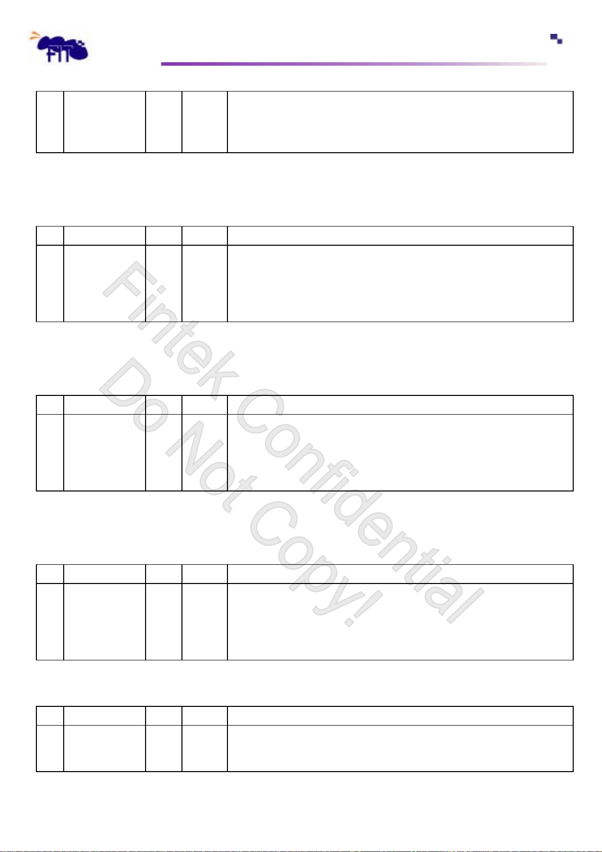
8.23 Address1 Decode Register (Low Byte) – Index 21h
Power-on default [7:0] =0000_0000b
Bit Name R/W PWR Description
7-0 ADDR_DEC1 R/W VDD3V
F85226F
This register contains the address for specify decoder.
24
Page 30
k
F
Finte
CR21 Bit [7..0] are used to define low byte of specify address.
CR22 Bit [7..0] are used to define high byte of specify address.
For example: Decoding address was set to be 0x3F5h when wrote F5h to CR21
and 03h to CR22.
Feature Integration Technology Inc.
F85226
8.24 Address1 Decode Register (High Byte) – Index 22h
Power-on default [7:0] =0000_0000b
Bit Name R/W PWR Description
7-0 ADDR_DEC1 R/W VDD3V
This register contains the address for specify decoder.
CR21 Bit [7..0] are used to define low byte of specify address.
CR22 Bit [7..0] are used to define high byte of specify address.
For example: Decoding address was set to be 0x3F5h when wrote F5h to CR21
and 03h to CR22.
8.25 Address2 Decode Mask Register – Index 23h
Power-on default [7:0] =0000_0000b
Bit Name R/W PWR Description
This register is used to mask address bits (A7~A0) for specify address decoder, if
the corresponding bit of this register is set to a 1, the corresponding address
7-0 ADDR_MASK2 R/W VDD3V
bit(A7~A0) is ignored by the specify address decoder.
For example: If the decoding range is 0x3F8 ~ 0x3FF, you can set 0x03F8 to CR24,
25 and 07h to CR23.
8.26 Address2 Decode Register (Low Byte) – Index 24h
Power-on default [7:0] =0000_0000b
Bit Name R/W PWR Description
This register contains the address for specify decoder.
CR24 Bit [7:0] are used to define low byte of specify address.
7-0 ADDR_DEC2 R/W VDD3V
CR25 Bit [7:0] are used to define high byte of specify address.
For example: Decoding address was set to be 0x3F5h when wrote F5h to CR24
and 03h to CR25.
8.27 Address2 Decode Register (High Byte) – Index 25h
Power-on default [7:0] =0000_0000b
Bit Name R/W PWR Description
This register contains the address for specify decoder.
7-0 ADDR_DEC2 R/W VDD3V
F85226F
CR24 Bit [7..0] are used to define low byte of specify address.
CR25 Bit [7..0] are used to define high byte of specify address.
25
Page 31
k
F
Finte
For example: Decoding address was set to be 0x3F5h when wrote F5h to CR24
and 03h to CR25 .
Feature Integration Technology Inc.
F85226
8.28 ROM1 Decoder Mask Low Byte Register – Index 0x28
Power-on default [7:0] =0000_0000b
Bit Name R/W PWR Description
The register CR28, 29 are used to mask address bits (A19~A4) for specify address
decoder, if the corresponding bit of this register is set to a 1, the corresponding
7-0 ROM_MASK1 R/W VDD3V
address bit(A19~A4) is ignored by the specify address decoder.
For example: If the decoding range is 0xF_FFFX ~ 0xF_E00X, you can set
0xF_FFFF to CR2A, 2B and ffh to CR28, 01h to CR29.
8.29 ROM Decoder Mask (High Byte) Register – Index 0x29
Power-on default [7:0] =0000_0000b
Bit Name R/W PWR Description
The register CR28, 29 are used to mask address bits (A19~A4) for specify address
decoder, if the corresponding bit of this register is set to a 1, the corresponding
7-0 ROM_ MASK1 R/W VDD3V
address bit(A19~A4) is ignored by the specify address decoder.
For example: If the decoding range is 0xF_FFFX ~ 0xF_E00X, you can set
0xF_FFFF to CR2A, 2B and ffh to CR28, 01h to CR29.
8.30 ROM Decoder Address (Low Byte) Register – Index 0x2A
Power-on default [7:0] =0000_0000b
Bit Name R/W PWR Description
This register contains the address for specify decoder.
CR2A Bit [7..0] are used to define low address[11:4].
7-0 ROM_DEC1 R/W VDD3V
CR2B Bit [7..0] are used to define high address[19:12].
For example: Decoding address was set to be 0xF_FEEXh when wrote EEh to
CR2A and FFh to CR2B.
8.31 ROM Decoder Address (High Byte) Register – Index 0x2B
Power-on default [7:0] =0000_0000b
Bit Name R/W PWR Description
This register contains the address for specify decoder.
CR2A Bit [7..0] are used to define low address[11:4].
7-0 ROM_DEC1 R/W VDD3V
F85226F
CR2B Bit [7..0] are used to define high address[19:12].
For example: Decoding address was set to be 0xF_FEEXh when wrote EEh to
CR2A and FFh to CR2B.
26
Page 32

k
F
Finte
Feature Integration Technology Inc.
F85226
8.32 ROM2 Decoder Mask Low Byte Register – Index 0x2C
Power-on default [7:0] =0000_0000b
Bit Name R/W PWR Description
The register CR2C, 2D are used to mask address bits (A19~A4) for specify address
decoder, if the corresponding bit of this register is set to a 1, the corresponding
7-0 ROM_MASK2 R/W VDD3V
address bit(A19~A4) is ignored by the specify address decoder.
For example: If the decoding range is 0xF_FFFX ~ 0xF_E00X, you can set
0xF_FFFF to CR2E, 2F and ffh to CR2C, 01h to CR2D.
8.33 ROM2 Decoder Mask (High Byte) Register – Index 0x2D
Power-on default [7:0] =0000_0000b
Bit Name R/W PWR Description
The register CR2C, 2D are used to mask address bits (A19~A4) for specify address
decoder, if the corresponding bit of this register is set to a 1, the corresponding
7-0 ROM_ MASK2 R/W VDD3V
address bit(A19~A4) is ignored by the specify address decoder.
For example: If the decoding range is 0xF_FFFX ~ 0xF_E00X, you can set
0xF_FFFF to CR2E, 2F and ffh to CR2C, 01h to CR2D.
8.34 ROM2 Decoder Address (Low Byte) Register – Index 0x2E
Power-on default [7:0] =0000_0000b
Bit Name R/W PWR Description
This register contains the address for specify decoder.
CR2E Bit [7..0] are used to define low address[11:4].
7-0 ROM_DEC2 R/W VDD3V
CR2F Bit [7..0] are used to define high address[19:12].
For example: Decoding address was set to be 0x5_5AAXh when wrote AAh to
CR2E and 55h to CR2F.
8.35 ROM2 Decoder Address (High Byte) Register – Index 0x2F
Power-on default [7:0] =0000_0000b
Bit Name R/W PWR Description
This register contains the address for specify decoder.
CR2E Bit [7..0] are used to define low address[11:4].
7-0 ROM_DEC2 R/W VDD3V
F85226F
CR2F Bit [7..0] are used to define high address[19:12].
For example: Decoding address was set to be 0x5_5AAXh when wrote AAh to
CR2E and 55h to CR2F.
27
Page 33
k
F
Finte
Feature Integration Technology Inc.
F85226
8.36 ADDR3 Decoder Mask High Byte Register – Index 0x30
Power-on default [7:0] =0000_0000b
Bit Name R/W PWR Description
This register is used to mask io address bits A7~A0 or memory addrss bits
A23~A16 for specify address decoder, if the corresponding bit of this register is set
7-0 ADDR3_DEC_MASK R/W VDD3V
to a 1, the corresponding address bits will ignored by the specify address decoder.
For example: If the decoding range is 0x3F8 ~ 0x3FF, you can set 0x03F8 to CR31,
32 and 07h to CR30.
8.37 ADDR3 Decoder Address Low Byte Register – Index 0x31
Power-on default [7:0] =0000_0000b
Bit Name R/W PWR Description
This register contains the address for specify decoder.
CR31 Bit [7..0] are used to define low byte of specify address.
CR32 Bit [7..0] are used to define high byte of specify address.
7-0 ADDR3_DEC R/W VDD3V
For example: Decoding address was set to be 0x3F5h when wrote F5h to CR31
and 03h to CR32. (The address decoder will decode the match “IO” address that
define in CR31 and CR32 register, but when set CR1B bit6 to 1, The address
decoder will decode the match “memory” address[31:16] that define in CR31 and
CR32 registers).
8.38 ADDR3 Decoder Address High Byte Register – Index 0x32
Power-on default [7:0] =0000_0000b
Bit Name R/W PWR Description
This register contains the address for specify decoder.
CR31 Bit [7..0] are used to define low byte of specify address.
CR32 Bit [7..0] are used to define high byte of specify address.
7-0 ADDR3_DEC R/W VDD3V
For example: Decoding address was set to be 0x3F5h when wrote F5h to CR31
and 03h to CR32. (The address decoder will decode the match “IO” address that
define in CR31 and CR32 register, but when set CR1B bit6 to 1, The address
decoder will decode the match “memory” address[31:16] that define in CR31 and
CR32 registers).
8.39 ADDR4 Decoder Mask High Byte Register – Index 0x33
Power-on default [7:0] =0000_0000b
Bit Name R/W PWR Description
7-0
ADDR4_DEC_MASK
R/W VDD3V
F85226F
This register is used to mask io address bits A7~A0 or memory addrss bits
28
Page 34

k
F
Finte
A23~A16 for specify address decoder, if the corresponding bit of this register is set
to a 1, the corresponding address bits will ignored by the specify address decoder.
For example: If the decoding range is 0x3F8 ~ 0x3FF, you can set 0x03F8 to CR34,
35 and 07h to CR33.
Feature Integration Technology Inc.
F85226
8.40 ADDR4 Decoder Address Low Byte Register – Index 0x34
Power-on default [7:0] =0000_0000b
Bit Name R/W PWR Description
7-0 ADDR4_DEC R/W VDD3V
This register contains the address for specify decoder.
CR34 Bit [7..0] are used to define low byte of specify address.
CR35 Bit [7..0] are used to define high byte of specify address.
For example: Decoding address was set to be 0x3F5h when wrote F5h to CR34
and 03h to CR35. (The address decoder will decode the match “IO” address that
define in CR34 and CR35 register, but when set CR1B bit7 to 1, The address
decoder will decode the match “memory” address[31:16] that define in CR34 and
CR35 registers).
8.41 ADDR4 Decoder Address High Byte Register – Index 0x35
Power-on default [7:0] =0000_0000b
Bit Name R/W PWR Description
This register contains the address for specify decoder.
CR34 Bit [7..0] are used to define low byte of specify address.
CR35 Bit [7..0] are used to define high byte of specify address.
7-0 ADDR4_DEC R/W VDD3V
For example: Decoding address was set to be 0x3F5h when wrote F5h to CR34
and 03h to CR35. (The address decoder will decode the match “IO” address that
define in CR34 and CR35 register, but when set CR1B bit7 to 1, The address
decoder will decode the match “memory” address[31:16] that define in CR34 and
CR35 registers).
8.42 KBC Decoder Mask Register – Index 0x36
Power-on default [7:0] =0000_0100b
Bit Name R/W PWR Description
This register is used to mask address bits (A7~A0) for specify address decoder, if
the corresponding bit of this register is set to a 1, the corresponding address
7-0 KBC _MASK R/W VDD3V
bit(A7~A0) is ignored by the specify address decoder.
For example: If the decoding range is 0x060 & 0x064, you can set 0x060 to CR37,
38 and 04h to CR36.
F85226F
29
Page 35

k
F
Finte
Feature Integration Technology Inc.
F85226
8.43 KBC Decoder Address Low Byte Register – Index 0x37
Power-on default [7:0] =0110_0000b
Bit Name R/W PWR Description
This register contains the address for KBC decoder.
CR37 Bit [7..0] are used to define low byte of specify address.
7-0 KBC_DEC R/W VDD3V
8.44 KBC Decoder Address High Byte Register – Index 0x38
Power-on default [7:0] =0000_0000b
Bit Name R/W PWR Description
7-0 KBC_DEC R/W VDD3V
CR38 Bit [7..0] are used to define high byte of specify address.
For example: Decoding address was set to be 0x060h when wrote 60h to CR37 and
00h to CR38.
This register contains the address for KBC decoder.
CR37 Bit [7..0] are used to define low byte of specify address.
CR38 Bit [7..0] are used to define high byte of specify address.
For example: Decoding address was set to be 0x060h when wrote 60h to CR37 and
00h to CR38.
8.45 MC Decoder Mask Register – Index 0x39
Power-on default [7:0] =0000_0100b
Bit Name R/W PWR Description
This register is used to mask address bits (A7~A0) for specify address decoder, if
the corresponding bit of this register is set to a 1, the corresponding address
7-0 MC _MASK R/W VDD3V
bit(A7~A0) is ignored by the specify address decoder.
For example: If the decoding range is 0x062 & 0x066, you can set 0x062 to CR3A,
3B and 04h to CR39.
8.46 MC Decoder Address Low Byte Register – Index 0x3A
Power-on default [7:0] =0110_0010b
Bit Name R/W PWR Description
7-0 MC_DEC R/W VDD3V
This register contains the address for KBC decoder.
CR3A Bit [7..0] are used to define low byte of specify address.
CR3B Bit [7..0] are used to define high byte of specify address.
For example: Decoding address was set to be 0x062h when wrote 60h to CR3A and
00h to CR3B.
F85226F
30
Page 36

k
F
Finte
Feature Integration Technology Inc.
F85226
8.47 MC Decoder Address High Byte Register – Index 0x3B
Power-on default [7:0] =0000_0000b
Bit Name R/W PWR Description
This register contains the address for KBC decoder.
CR3A Bit [7..0] are used to define low byte of specify address.
7-0 MC_DEC R/W VDD3V
8.48 RTC Decoder Mask Register – Index 0x3C
Power-on default [7:0] =0000_0001b
Bit Name R/W PWR Description
7-0 RTC_ MASK R/W VDD3V
CR3B Bit [7..0] are used to define high byte of specify address.
For example: Decoding address was set to be 0x062h when wrote 60h to CR3A and
00h to CR3B.
This register is used to mask address bits (A7~A0) for specify address decoder, if
the corresponding bit of this register is set to a 1, the corresponding address
bit(A7~A0) is ignored by the specify address decoder.
For example: If the decoding range is 0x070 & 0x071, you can set 0x070 to CR3D,
3E and 01h to CR3C.
8.49 RTC Decoder Address Low Byte Register – Index 0x3D
Power-on default [7:0] =0111_0000b
Bit Name R/W PWR Description
This register contains the address for KBC decoder.
CR3D Bit [7..0] are used to define low byte of specify address.
7-0 RTC_DEC R/W VDD3V
CR3E Bit [7..0] are used to define high byte of specify address.
For example: Decoding address was set to be 0x060h when wrote 70h to CR3D
and 00h to CR3E.
8.50 RTC Decoder Address High Byte Register – Index 0x3E
Power-on default [7:0] =0000_0000b
Bit Name R/W PWR Description
This register contains the address for KBC decoder.
CR3D Bit [7..0] are used to define low byte of specify address.
7-0 RTC_DEC R/W VDD3V
CR3E Bit [7..0] are used to define high byte of specify address.
For example: Decoding address was set to be 0x060h when wrote 70h to CR3D
and 00h to CR3E.
F85226F
31
Page 37
k
F
Finte
Feature Integration Technology Inc.
F85226
8.51 IOH Decoder Mask Register – Index 0x3F
Pow er-on default [ 7:0] =1111_1111b
Bit Name R/W PWR Description
This register is used to mask address bits (A7~A0) for specify address decoder, if
the corresponding bit of this register is set to a 1, the corresponding address
7-0 IOH_ MASK R/W VDD3V
8.52 IOH Decoder Address Low Byte Register – Index 0x40
bit(A7~A0) is ignored by the specify address decoder.
For example: If the decoding range is 0x0000 ~ 0x00FF, you can set 0x00 to
CR40, 41 and FFh to CR3F.
Power-on default [7:0] =0000_0000b
Bit Name R/W PWR Description
This register contains the address for KBC decoder.
CR40 Bit [7..0] are used to define low byte of specify address.
7-0 IOH_DEC R/W VDD3V
CR41 Bit [7..0] are used to define high byte of specify address.
For example: Decoding address was set to be 0x0080h when wrote 80h to CR40
and 00h to CR41.
8.53 IOH Decoder Address High Byte Register – Index 0x41
Power-on default [7:0] =0000_0000b
Bit Name R/W PWR Description
This register contains the address for KBC decoder.
CR40 Bit [7..0] are used to define low byte of specify address.
7-0 IOH_DEC R/W VDD3V
CR41 Bit [7..0] are used to define high byte of specify address.
For example: Decoding address was set to be 0x0080h when wrote 80h to CR40
and 00h to CR41.
8.54 Edge Detector Status Register – Index 0x50
Power-on default [7:0] =0000_0000b
Bit Name R/W PWR Description
7-1 Reserved RO VDD3V Reserved
0 CLK_PD RW VDD3V Set to 1 to disable SYSCLK output.
F85226F
32
Page 38
k
F
Finte
Feature Integration Technology Inc.
F85226
8.55 IRQ Wakeup Register (I) – Index 0x51
Power-on default [7:0] =0000_0000b
Bit Name R/W PWR Description
7 EN_IRQ7_W RW VDD3V Set to 1 to enable IRQ7 to wakeup the system.
6 EN_IRQ6_W R/W VDD3V Set to 1 to enable IRQ6 to wakeup the system.
5 EN_IRQ5_W R/W VDD3V Set to 1 to enable IRQ5 to wakeup the system.
4 EN_IRQ4_W R/W VDD3V Set to 1 to enable IRQ4 to wakeup the system.
3 EN_IRQ3_W R/W VDD3V Set to 1 to enable IRQ3 to wakeup the system.
2 Reserved R/W VDD3V Reserved
1 EN_IRQ1_W R/W VDD3V Set to 1 to enable IRQ1 to wakeup the system.
0 EN_PWRDN_W RW VDD3V Set to 1 to enable PWRDN pin to power down or wakeup the system.
8.56 IRQ Wakeup Register (II) – Index 0x52
Power-on default [7:0] =0000_0000b
Bit Name R/W PWR Description
7 Reserved RW VDD3V Reserved
6 EN_IRQ15_W R/W VDD3V Set to 1 to enable IRQ15 to wakeup the system.
5 EN_IRQ14_W R/W VDD3V Set to 1 to enable IRQ14 to wakeup the system.
4 EN_IRQ12_W R/W VDD3V Set to 1 to enable IRQ12 to wakeup the system.
3 EN_IRQ11_W R/W VDD3V Set to 1 to enable IRQ11 to wakeup the system.
2 EN_IRQ10_W R/W VDD3V Set to 1 to enable IRQ10 to wakeup the system.
1 EN_IRQ9_W R/W VDD3V Set to 1 to enable IRQ9 to wakeup the system.
0 EN_IRQ8_W RW VDD3V Set to 1 to enable IRQ8 to wakeup the system.
8.57 CHIPID (1) Register – Index 5Ah
Power-on default [7:0] =0000_0011b
Bit Name R/W PWR Description
7-0 CHIPID RO VDD3V Chip ID, High byte (8’h03).
8.58 CHIPID (2) Register – Index 5Bh
Power-on default [7:0] =0000_0101b
Bit Name R/W PWR Description
7-0 CHIPID RO VDD3V Chip ID, Low byte (8’h05).
F85226F
33
Page 39
k
F
Finte
Feature Integration Technology Inc.
F85226
8.59 VERSION Register – Index 5Ch
Power-on default [7:0] =0001_0000b
Bit Name R/W PWR Description
7-0 VERSION RO VDD3V Version 1.0.
8.60 VENDOR ID (1) Register – Index 5Dh
Power-on default [7:0] =0001_1001b
Bit Name R/W PWR Description
7-0 VENDOR1 RO VDD3V Vendor ID, 8’h19.
8.61 VENDOR ID (2) Register – Index 5Eh
Power-on default [7:0] =0011_0100b
Bit Name R/W PWR Description
7-0 VENDOR2 RO VDD3V Vendor ID, 8h34.
9. Electrical characteristic
9.1 Absolute Maximum Ratings
PARAMETER RATING UNIT
Power Supply Voltage -0.5 to 5.5 V
Input Voltage -0.5 to VDD+0.5 V
Operating Temperature 0 to +70 ° C
Storage Temperature -55 to 150 ° C
Note: Exposure to conditions beyond those listed under Absolute Maximum Ratings may adversely affect
the life and reliability of the device
F85226F
34
Page 40

k
F
Finte
Feature Integration Technology Inc.
F85226
9.2 DC Characteristics
(Ta = 70° C, VDD = 3.3V, VSS = 0V)
PARAMETER SYM. MIN. TYP. MAX. UNIT CONDITIONS
I/OD
source-sink capability
Input Low Threshold Voltage Vt- 0.8 V VDD = 3.3 V
Input High Threshold Voltage Vt+ 2.0 V VDD = 3.3 V
Output Low Current IOL 24 mA VOL = 0.4 V
Input High Leakage ILIH 1
Input Low Leakage ILIL -1
I/O24
Input Low Threshold Voltage Vt- 0.8 V VDD = 3.3 V
- TTL level bi-directional pin, with Schmitt trigger, can select to O D by register, with 24 mA
24ts
µA
- TTL level bi-directional pin, with Schmitt trigger and 24 mA source-sink capability
ts
µA
VIN = VDD
VIN = 0V
Input High Threshold Voltage Vt+ 2.0 V VDD = 3.3 V
Output High Current IOH -24 mA VOL = 2.4 V
Output Low Current IOL 24 mA VOL = 0.4 V
Input High Leakage ILIH 1
Input Low Leakage ILIL -1
O20 - Output pin with 20 mA source-sink capability
Output High Current IOH -20 mA VOL = 2.4 V
Output Low Current IOL 20 mA VOL = 0.4 V
O24 - Output pin with 24 mA source-sink capability
Output High Current IOH -24 mA VOL = 2.4 V
Output Low Current IOL 24 mA VOL = 0.4 V
INt - TTL level input pin
Input Low Threshold Voltage Vt- 0.8 V VDD = 3.3 V
Input High Threshold Voltage Vt+ 2.0 V VDD = 3.3 V
Input High Leakage ILIH 1
Input Low Leakage ILIL -1
µA
µA
µA
µA
VIN = VDD
VIN = 0V
VIN = VDD
VIN = 0V
INts - TTL level input pin with schmitt trigger
Input Low Threshold Voltage Vt- 0.8 V VDD = 3.3 V
Input High Threshold Voltage Vt+ 2.0 V VDD = 3.3 V
Input High Leakage ILIH 1
Input Low Leakage ILIL -1
F85226F
35
µA
µA
VIN = VDD
VIN = 0V
Page 41
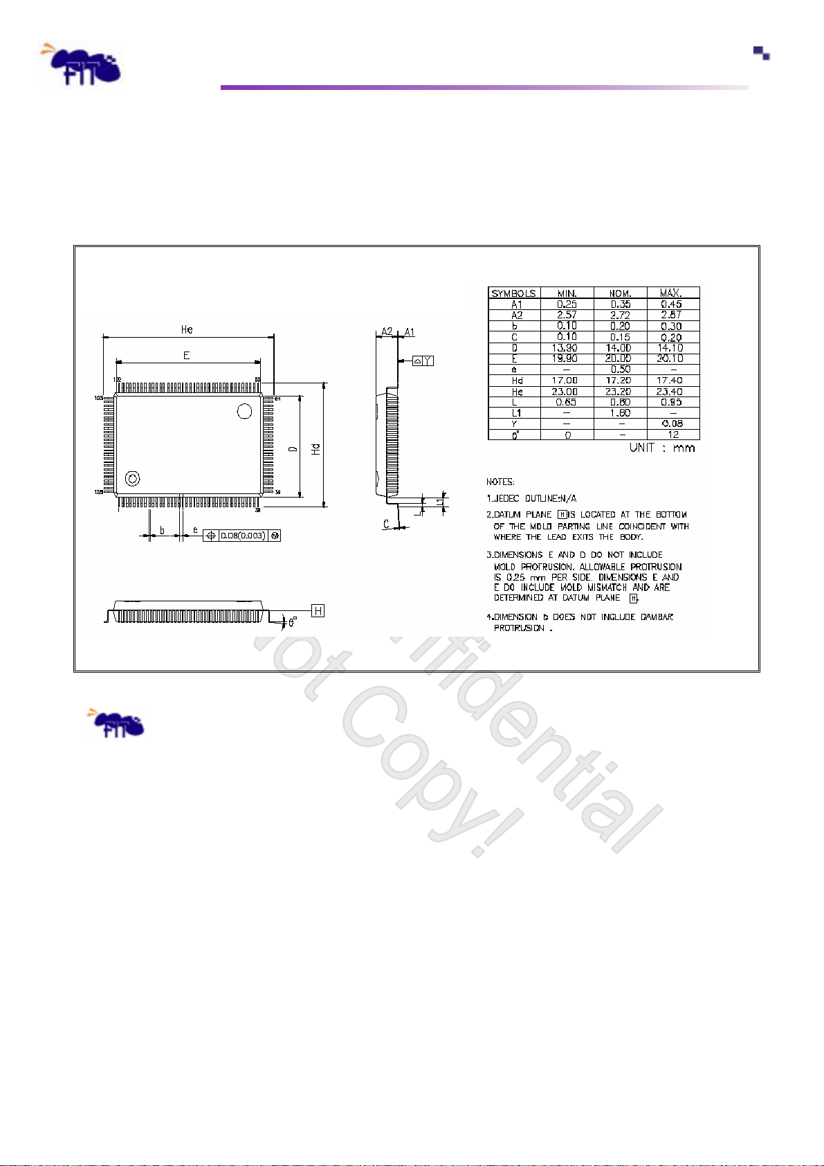
k
F
Finte
Feature Integration Technology Inc.
F85226
10. Package specification
128 PQFP
Headquaters
7F, No 31, Shintai Rd,
Jubei City, Hsinchu 302, Taiwan, R.O.C.
TEL: 886-3-6562727
FAX: 886-3-6560537
www: http://www.fintek.com.tw
Feature Integration Technology Inc.
Taipei Office
Bldg K4, 7F, No. 700, Chung Cheng Rd,
Chungho City, Taipei 235, Taiwan, R.O.C.
TEL: 886-2-8227-8027
FAX: 886-2-8227-803 7
Please note that all datasheet and specifications are subject to change without notice. All the trade
marks of products and companies mentioned in this datasheet belong to their respective owne
r.
F85226F
36
Page 42
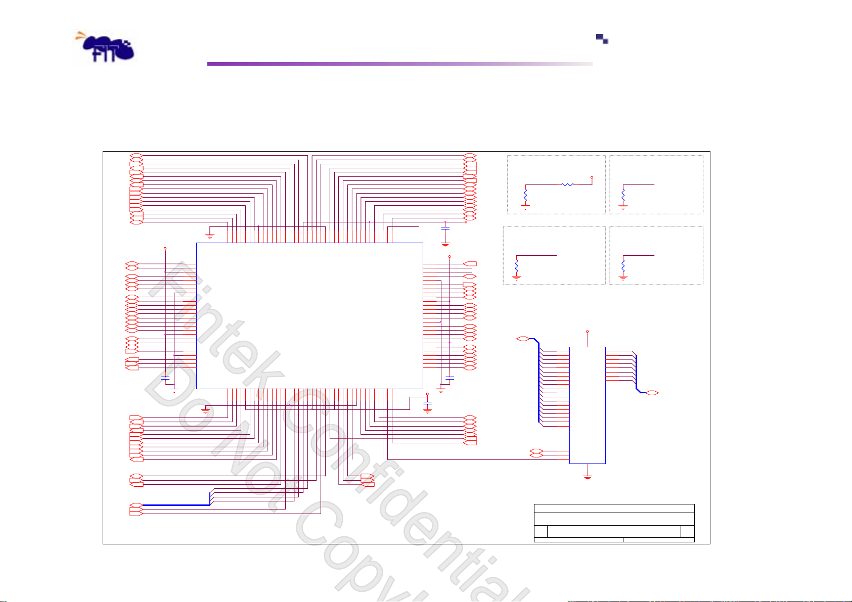
k
F
Finte
Feature Integration Technology Inc.
F85226
11. Application Circuit
C1
0.1u
GP15
GP14
GP13
GP12
GP11
SMEMR#
VCC3V
SMEMW#
OWS#
DRQ2
IRQ9
RSTDRV
IOCHCK#
SD7
SD6
SD5
SD4
SD3
SD2
SD1
SD0
RTCCS#
ROM_EN SELECT
ROM EN
R5
R1 ON ROM_EN ON
10K
R1 OFF ROM_EN OFF
R1 4.7K
4E_EN SELECT
4E EN
R3
IRQ8
10K
R3 ON ACCESS PORT = 2Eh
IOCHRDY
AEN
SA19
SA18
SA17
SA16
SA15
SA14
SA13
SA12
SA11
SA10
SA9
SA8
SA7
SA6
SA5
MCCS#
KBCS#
C3
0.1u
SA4
SA3
SA2
SA1
SA0
PWR_PD
IRQ1
R3 OFF ACCESS PORT = 4Eh
SA[18..0]
MEMW#
MEMR#
Titl e
Size Document Number Rev
Date: Sheet
1
30
2
3
29
28
4
25
23
26
27
5
6
7
8
9
10
11
12
31
24
22
F85226F Application C ircuit
<Doc> <RevC ode>
B
IOW#
IOR#
DACK3#
DRQ3
DACK1#
DRQ1
REFRESH #
SYSCLK
IRQ7
IRQ6
IRQ5
IRQ4
IRQ3
DACK2#
BALE
SBHE#
LA23
LA22
LA21
LA20
LA19
LA18
LA17
MEMR #
MEMW#
SD8
SD9
SD10
SD11
SD12
SD13
SD14
SD15
MASTER#
DRQ7
DACK7#
DRQ6
DACK6#
DRQ5
DACK5#
DRQ0
DACK0#
IRQ14
IRQ15
IRQ12
IRQ11
IRQ10
IOCS16#
MEMC S16#
SERIRQ
PCICLK
LFRAM#
LAD[3.. 0]
PCIRST#
LDRQ#
TC
100
101
102
U1
TC
GND
IRQ7
IRQ6
IRQ5
IRQ4
IRQ3
BALE
SBHE#
103
LA23
104
LA22
105
VCC7
106
LA21
107
LA20
108
LA19
109
LA18
110
GND
111
LA17
112
MEMR #
113
MEMW#
114
SD8
115
SD9
116
SD10
117
SD11
118
SD12
119
SD13
120
VCC8
121
SD14
122
SD15
123
MASTER#
124
DRQ7
125
GND
126
DACK7#
127
DRQ6
128
DACK6#
F85226F
DACK2#
DRQ5
DACK5#
DRQ0
DACK0#
VCC1
IRQ14
IRQ15
12345678910111213141516171819202122232425262728293031323334353637
LAD0
LAD1
LAD2
LAD3
IRQ12
DRQ3
DRQ1
DACK3#
DACK1#
SYSCLK
REFRESH #
IRQ11
IRQ10
IOCS16#
MEMCS16#
LFRAM#
LRESET#
GND
LAD3
GND
IOR#
VCC6
LAD2
LAD1
IRQ9
IOW#
DRQ2
OWS#
SMEMR#
SMEMW#
LAD0
VCC2
PCICLK
LDRQ#
SERIRQ
LPC_PD#
VCC3
SD3
SD4
SD5
SD6
SD7
VCC5
IOCHK#
RSTDRV
CLKIN
CLKOUT1
CLKOUT2
GP23
GND
SA0
SA1
SA2
GP23
RTC_EN
4E_EN
VCC3V
C2
0.1u
SD0
SD1
SD2
SA3
SA4
80CS#/KBEN#
KB_EN
CLKOUT2
CLKOUT1
14.318M
6566676869707172737475767778798081828384858687888990919293949596979899
GPIO5/IRQ8
GPIO7/ IOCS#
GPIO4/PLED
GPIO6/RTCCS#
GPIO3/IRQIN
GPIO2/MSCS#
GPIO1/KBCS#
ROMCS#
GPIO0/ IRQ1
38
ROM_EN
GP16
GP17
IOCHRDY
GND
AEN
SA19
SA18
SA17
VCC
SA16
SA15
SA14
SA13
GND
SA12
SA11
SA10
VCC4
VCC3V
64
63
62
61
60
59
58
57
56
55
54
53
52
51
50
49
48
47
46
SA9
45
44
SA8
43
SA7
42
SA6
41
SA5
40
39
VCC3V
C4
0.1u
A18
A17
A16
A15
A14
A13
A12
A11
A10
A9
A8
A7
A6
A5
A4
A3
A2
A1
A0
WE#
OE#
CE#
VCC3V
VCC3V
3216
KB_EN SELECT
KB EN
R2
R2 ON KB_EN ON
10K
R2 OFF KB_EN OFF
RTC_EN SELECT
RTC EN
R4
R4 ON RTC_EN ON
10K
R4 OFF RTC_EN OFF
U2
13
DQ0
14
DQ1
VCCGND
15
DQ2
17
DQ3
18
DQ4
19
DQ5
20
DQ6
21
DQ7
SD[7..0]
of
13Monday, August 16, 2004
F85226F
37
Page 43
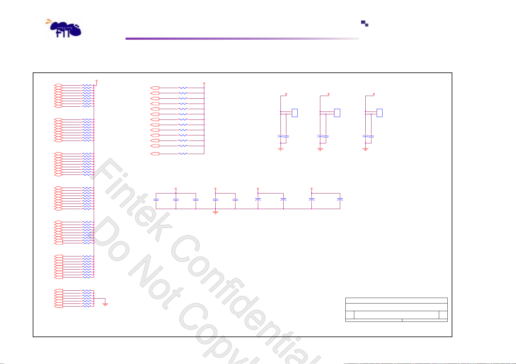
k
F
Finte
Feature Integration Technology Inc.
F85226
VCC5V
SA19
SA18
SA17
SA16
SA15
SA14
SA13
SA12
SA11
SA10
SA9
SA8
SA7
SA6
SA5
SA4
SA3
SA2
SA1
SA0
LA23
LA22
LA21
LA20
LA19
LA18
LA17
SD0
SD1
SD2
SD3
SD4
SD5
SD6
SD7
SD8
SD9
SD10
SD11
SD12
SD13
SD14
SD15
IRQ14
IRQ15
IRQ3
IRQ4
IRQ5
IRQ6
IRQ7
IRQ9
IRQ10
IRQ11
IRQ12
DRQ0
DRQ1
DRQ2
DRQ3
DRQ5
DRQ6
DRQ7
R20
R21
R23
R24
R26
R
R27
R
R29
R
R30
R
R32
R
R
R
R
R
R35
R37
R38
R40
R41
R
R43
R
R44
R
R46
R
R47
R
R
R
R
R
R50
R52
R53
R54
R55
R
R56
R
R57
R
R58
R
R59
R
R
R
R
R
R60
R61
R62
R63
R64
R
R65
R
R66
R
R67
R
R68
R
R
R
R
R
R69
R70
R71
R72
R73
R
R74
R
R75
R
R76
R
R77
R
R
R
R
R
R78
R79
R80
R81
R82
R
R83
R
R84
R
R85
R
R86
R
R
R
R
R
R87
R88
R89
R90
R91
R
R92
R
R93
R
R
R
R
R
IOCHCK#
OWS#
IOCHRDY
MASTE R#
REFRESH#
IOR#
MEMR #
MEMCS 16#
IOCS16#
SMEMR#
SMEMW#
IOW#
MEMW#
C14
0.1u
R22 4.7K
R25 1K
R28 1K
R31 8.2K
R33 1K
R34 8.2K
R36 8.2K
R39 1K
R42 1K
R45 1K
R48 1K
R49
R51
VCC5V
C15
0.1u
8.2K
8.2K
C16
0.1u
VCC5V
VCC3V
+12V
J4
1
2
CON2
C8
VCC5V
C17
0.1u
C18
0.1u
C19
10u
C9
0.1u
10u
C20
10u
C10
10u
VCC3V
-12V
J5
1
2
CON2
C11
0.1u
C21
10u
C22
10u
Tit le
Size Document Number Rev
Date: Sheet
-5V
J6
1
2
CON2
C12
10u
F85226F Application Circuit
<Doc> <Rev Code>
B
C13
0.1u
of
23Tuesday, December 23, 2003
F85226F
38
Page 44
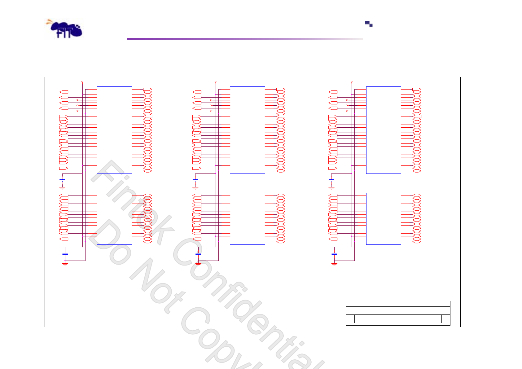
k
F
Finte
Feature Integration Technology Inc.
F85226
VCC5V
-5V
-12V
+12V
C25
0.1u
C28
0.1u
RSTDRV
IRQ9
DRQ2
OWS#
SMEMW#
SMEMR#
IOW#
IOR#
DACK3#
DRQ3
DACK1#
DRQ1
SYSCLK
IRQ7
IRQ6
IRQ5
IRQ4
IRQ3
DACK2#
BALE
OSC
MECS16#
IOCS16#
IRQ10
IRQ12
IRQ15
IRQ14
DACK0#
DRQ0
DACK5#
DRQ5
DACK6#
DRQ6
DACK7#
DRQ7
MASTER#
VCC5V
J7
33 2
RESDRV SD7
34
+5V
35
IRQ9
36
37
38
39
40
41
42
43
44
45
46
47
48
49
50
51
52
53
54
55
56
57
58
59
60
61
62
19
20
21
22
23
24
25
26
27
28
29
30
31
32
33
34
35
-5V
DRQ2
-12V
0WS
+12V
GND
SMEMW#
SMEMR#
IOW#
IOR#
DACK3#
DRQ3
DACK1#
DRQ1
REF#
CLK
IRQ7
IRQ6
IRQ5
IRQ4
IRQ3
DACK2#
T/C
BALE
+5
OSC
GND
A/B CH ANNEL
J10
MECS16#
IOCS16#
IRQ10
IRQ11
IRQ12
IRQ15
IRQ14
DACK0#
DRQ0
DACK5#
DRQ5
DACK6#
DRQ6
DACK7#
DRQ7
+5V
MASTER#
C/D CHANNEL
-5V
+12V
TC
C23
0.1u
C26
0.1u
IOCHCK#GND
SD6
SD5
SD4
SD3
SD2
SD1
SD0
IORDY
AEN
SA19
SA18
SA17
SA16
SA15
SA14
SA13
SA12
SA11
SA10
SBHE
LA23
LA22
LA21
LA20
LA19
LA18
LA17
MEMR #
MEMW#
SD08
SD09
SD10
SD11
SD12
SD13
SD14
SD15GND
132
3
4
5
6
7
8
9
10
11
12
13
14
15
16
17
18
19
20
21
22
SA9
23
SA8
24
SA7
25
SA6
26
SA5
27
SA4
28
SA3
29
SA2
30
SA1
31
SA0
1
2
3
4
5
6
7
8
9
10
11
12
13
14
15
16
17
1836
IOCHCK#
SD7
SD6
SD5
SD4
SD3
SD2
SD1
SD0
IOCHRDY
AEN
SA19
SA18
SA17
SA16
SA15
SA14
SA13
SA12
SA11
SA10
SA9
SA8
SA7
SA6
SA5
SA4
SA3
SA2
SA1
SA0
SBHE#
LA23
LA22
LA21
LA20
LA19
LA18
LA17
MEMR #
MEMW #
SD8
SD9
SD10
SD11
SD12
SD13
SD14
SD15
RSTDRV
IRQ9
DRQ2
OWS#
SMEMW#
SMEMR#
IOW#
IOR#
DACK3#
DRQ3
DACK1#
DRQ1
SYSCLK
IRQ7
IRQ6
IRQ5
IRQ4
IRQ3
DACK2#
BALE
OSC
MEC S16#
IOCS16#
IRQ10
IRQ11
IRQ12
IRQ15
IRQ14
DACK0#
DRQ0
DACK5#
DRQ5
DACK6#
DRQ6
DACK7#
DRQ7
MASTER#
TC
C24
0.1u
C27
0.1u
-12V
+12V
VCC5V
J8
33 2
RESDRV SD7
34
+5V
35
IRQ9
-5V
36
-5V
37
DRQ2
38
-12V
39
0WS
40
+12V
41
GND
42
SMEMW#
43
SMEMR#
44
IOW#
45
IOR#
46
DACK3#
47
DRQ3
48
DACK1#
49
DRQ1
50
REF#
51
CLK
52
IRQ7
53
IRQ6
54
IRQ5
55
IRQ4
56
IRQ3
57
DACK2#
58
T/C
59
BALE
60
+5
61
OSC
62
GND
A/B CH ANNEL
J11
19
MECS16#
20
IOCS16#
21
IRQ10
22
IRQ11
23
IRQ12
24
IRQ15
25
IRQ14
26
DACK0#
27
DRQ0
28
DACK5#
29
DRQ5
30
DACK6#
31
DRQ6
32
DACK7#
33
DRQ7
34
+5V
35
MASTER #
C/D CHANNEL
IOCHCK#GND
MEMW#
SD6
SD5
SD4
SD3
SD2
SD1
SD0
IORDY
AEN
SA19
SA18
SA17
SA16
SA15
SA14
SA13
SA12
SA11
SA10
SA9
SA8
SA7
SA6
SA5
SA4
SA3
SA2
SA1
SA0
SBHE
LA23
LA22
LA21
LA20
LA19
LA18
LA17
MEMR #
SD08
SD09
SD10
SD11
SD12
SD13
SD14
SD15GN D
132
3
4
5
6
7
8
9
10
11
12
13
14
15
16
17
18
19
20
21
22
23
24
25
26
27
28
29
30
31
1
2
3
4
5
6
7
8
9
10
11
12
13
14
15
16
17
1836
IOCHCK#
SD7
SD6
SD5
SD4
SD3
SD2
SD1
SD0
IOCHRDY
AEN
SA19
SA18
SA17
SA16
SA15
SA14
SA13
SA12
SA11
SA10
SA9
SA8
SA7
SA6
SA5
SA4
SA3
SA2
SA1
SA0
SBHE#
LA23
LA22
LA21
LA20
LA19
LA18
LA17
MEMR #
MEMW #
SD8
SD9
SD10
SD11
SD12
SD13
SD14
SD15
RSTDRV
IRQ9
DRQ2
OWS#
SMEMW#
SMEMR#
IOW#
IOR#
DACK3#
DRQ3
DACK1#
DRQ1
SYSCLK
IRQ7
IRQ6
IRQ5
IRQ4
IRQ3
DACK2#
BALE
OSC
MECS 16#
IOCS16#
IRQ10
IRQ11IRQ11
IRQ12
IRQ15
IRQ14
DACK0#
DRQ0
DACK5#
DRQ5
DACK6#
DRQ6
DACK7#
DRQ7
MASTER#
TC
J9
33 2
RESDRV SD7
34
+5V
35
IRQ9
36
-5V
37
DRQ2
38
-12V
39
0WS
40
+12V
41
GND
42
SMEMW#
43
SMEMR#
44
IOW#
45
IOR#
46
DACK3#
47
DRQ3
48
DACK1#
49
DRQ1
50
REF#
51
CLK
52
IRQ7
53
IRQ6
54
IRQ5
55
IRQ4
56
IRQ3
57
DACK2#
58
T/C
59
BALE
60
+5
61
OSC
62
GND
A/B CHAN NEL
J12
19
MECS 16#
20
IOCS16#
21
IRQ10
22
IRQ11
23
IRQ12
24
IRQ15
25
IRQ14
26
DACK0#
27
DRQ0
28
DACK5#
29
DRQ5
30
DACK6#
31
DRQ6
32
DACK7#
33
DRQ7
34
+5V
35
MASTER#
C/D CHANNEL
IOCHCK#GND
SD6
SD5
SD4
SD3
SD2
SD1
SD0
IORDY
AEN
SA19
SA18
SA17
SA16
SA15
SA14
SA13
SA12
SA11
SA10
SA9
SA8
SA7
SA6
SA5
SA4
SA3
SA2
SA1
SA0
SBHE
LA23
LA22
LA21
LA20
LA19
LA18
LA17
MEMR #
MEMW#
SD08
SD09
SD10
SD11
SD12
SD13
SD14
SD15GND
132
3
4
5
6
7
8
9
10
11
12
13
14
15
16
17
18
19
20
21
22
23
24
25
26
27
28
29
30
31
1
2
3
4
5
6
7
8
9
10
11
12
13
14
15
16
17
1836
IOCHCK#
SD7
SD6
SD5
SD4
SD3
SD2-12V
SD1
SD0
IOCHRDY
AEN
SA19
SA18
SA17
SA16
SA15
SA14
SA13
SA12
SA11
SA10
SA9
SA8
SA7
SA6
SA5
SA4
SA3
SA2
SA1
SA0
SBHE#
LA23
LA22
LA21
LA20
LA19
LA18
LA17
MEMR#
MEMW#
SD8
SD9
SD10
SD11
SD12
SD13
SD14
SD15
F85226F
39
Tit le
F85226F Applicat ion Circuit
Size Document Number Rev
<Doc> <Rev Code>
B
Date: Sheet
33Tuesday, December 23, 2003
of
 Loading...