

Page 1

F81216D
F81216D
LPC to 4 UART Datasheet
Release Date: July, 2004
Version: V0.26P
F81216D July, 2004
V0.26P
Page 2
F81216D Datasheet Revision History
Version Date Page Revision History
0.22P 2003/07/22
0.23P 2003/07/31 14 Updated WDT enable timer as power-on setting
48MHz clock input : 5 sec
0.24P 2003/09/12 3 Updated pin description(CLKIN: pin12)
0.25P 2003/09/16 32 Updated Application circuit
F81216D
24MHz clock input : 10 sec
0.26P 2004/7/29 3 Revised pin 2 description
Please note that all data and specifications are subject to change without notice. All the trade marks of products
and companies mentioned in this data sheet belong to their respective owners.
LIFE SUPPORT APPLICATIONS
These products are not designed for use in life support appliances, devices, or systems where malfunctio n of these
products can reasonably be expected to result in personal injury. Customers using or selling these products for
use in such applications do so at their own risk and agree to fully indemnify Fintek for any damages resulting from
F81216D July, 2004
V0.26P
Page 3

such improper use or sales.
Table of Content
F81216D
1. General Description
2. Feature List................................................................................................................................................1
3. Pin Configuration........................................................................................................................................2
4. Pin Description ...........................................................................................................................................3
4.1 ISA/LPC Interface..................................................................................................................................................3
4.2 UART Interface......................................................................................................................................................4
4.3 Power ....................................................................................................................................................................7
5. Functional Description
5.1 LPC Interface......................................................................................................................................................8
5.2 UART ..................................................................................................................................................................8
5.2.1 UART Port Register...................................................................................................................................9
5.3 IR Function........................................................................................................................................................13
5.4 Watch Dog Timer Function...............................................................................................................................14
5.4.1 Watchdog Port Register........................................................................................................................14
5.5 Serial IRQ .........................................................................................................................................................15
5.5.1 Start Frame..............................................................................................................................................15
5.5.2 IRQ/Data Frame ......................................................................................................................................15
....................................................................................................................................1
.................................................................................................................................8
5.5.3 Stop Frame..............................................................................................................................................16
6.
Register Description..................................................................................................................................17
6.1 Global Control Register ....................................................................................................................................19
6.1.1 Software Reset Register – index 02h......................................................................................................19
6.1.2 Logic Device Select Register – index 07h...............................................................................................19
6.1.3 Device ID Register– index 20h, 21h........................................................................................................19
6.1.4 Device Reversion Register– index 22h ...................................................................................................20
6.1.5 Vendor ID Register– index 23h, 24h........................................................................................................20
6.1.6 Clock Source Select Register – index 25h..............................................................................................20
6.1.8 Test Mode Register – index 2Fh..............................................................................................................20
6.2 UART 1 Device Control Register (LDN 0)...........................................................................................................21
6.2.1 Device Enable Register – index 30h...............................................................................................21
6.2.2 I/O Port Select Register – index 60h...............................................................................................21
6.2.3 I/O Port Select Register – index 61h...............................................................................................21
6.2.4 IRQ Channel Select Register – index 70h ............................................................................................21
6.2.5 UART 1 Clock Select Register – index F0h..........................................................................................22
F81216D July, 2004
V0.26P
Page 4

F81216D
6.2.6 IR1 Control Register – index F1h..........................................................................................................22
6.3 UART 2 Device Control Register (LDN 1)...........................................................................................................23
6.3.1 Device Enable Register – index 30h...............................................................................................23
6.3.2 I/O Port Select Register – index 60h...............................................................................................23
6.3.3 I/O Port Select Register – index 61h...............................................................................................23
6.3.4 IRQ Channel Select Register – index 70h ............................................................................................23
6.3.5 UART 2 Clock Select Register – index F0h..........................................................................................24
6.4 UART 3 Device Control Register (LDN 2)...........................................................................................................24
6.4.1 Device Enable Register – index 30h...............................................................................................24
6.4.2 I/O Port Select Register – index 60h...............................................................................................24
6.4.3 I/O Port Select Register – index 61h...............................................................................................24
6.4.4 IRQ Channel Select Register – index 70h ............................................................................................25
6.4.5 UART 3 Clock Select Register – index F0h..........................................................................................25
6.5 UART 4 Device Control Register (LDN 3)...........................................................................................................25
6.5.1 Device Enable Register – index 30h...............................................................................................25
6.5.2 I/O Port Select Register – index 60h...............................................................................................26
6.5.3 I/O Port Select Register – index 61h...............................................................................................26
6.5.4 IRQ Channel Select Register – index 70h ............................................................................................26
6.5.6 UART 4 Clock Select Register – index F0h..........................................................................................26
6.6 Watch Dog Timer Device Control Register (LDN 8) .........................................................................................27
6.6.1 Device Enable Register – index 30h...............................................................................................27
6.6.2 I/O Port Select Register – index 60h...............................................................................................27
6.6.3 I/O Port Select Register – index 61h...............................................................................................27
6.6.4 IRQ Channel Select Register – index 70h ......................................................................................27
6.6.5 Timer Status and Control Register – index F0h ..............................................................................28
6.6.6 Timer Count Number Register – index F1h.....................................................................................28
7. Electron Characteristic
7.1 Absolute Maximum Ratings..............................................................................................................................29
7.2 DC Characteristics...............................................................................................................................................29
8. Ordering Information
9. Package Dimensions ..............................................................................................................................31
10. Application Circuit .................................................................................................................................32
............................................................................................................................29
...............................................................................................................................30
F81216D July, 2004
V0.26P
Page 5

F81216D
1. General Description
The F81216D mainly provides 3 pure UART ports and one UAR T+ IR port through LPC.
Each UART includes 16-byte send/receive FIFO, a programmable baud rate generator,
complete modem control capability and an interrupt system.
One watch dog timer is provided for system controlling and the time interval can be
programmed by register or hardware power on setting pin. One clock 24/48MHz input is
necessary, and default is 24MHz. Powered by 3.3V voltage, the F81216D is in the small
48pin LQFP package (7mm x 7mm).
2. Feature List
Supports LPC interface
Totally provides 4 UART (16550 asynchronous) ports
¾ 3 Pure UART
¾ 1 UART+IR
1 watch dog timer with WDTOUT# signal
1 frequency input 24/48MHz
Powered by 3Vcc
48-LQFP(7mm x 7mm)
-1-
July, 2004
V0.26P
Page 6
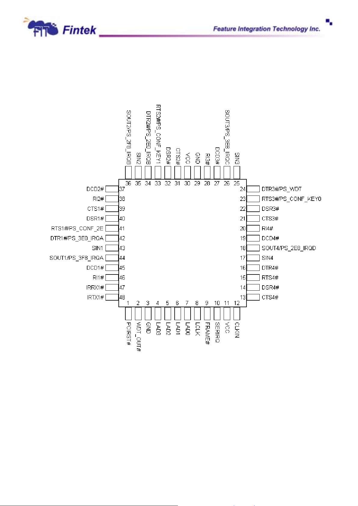
3. Pin Configuration
F81216D
F81216D
-2-
July, 2004
V0.26P
Page 7
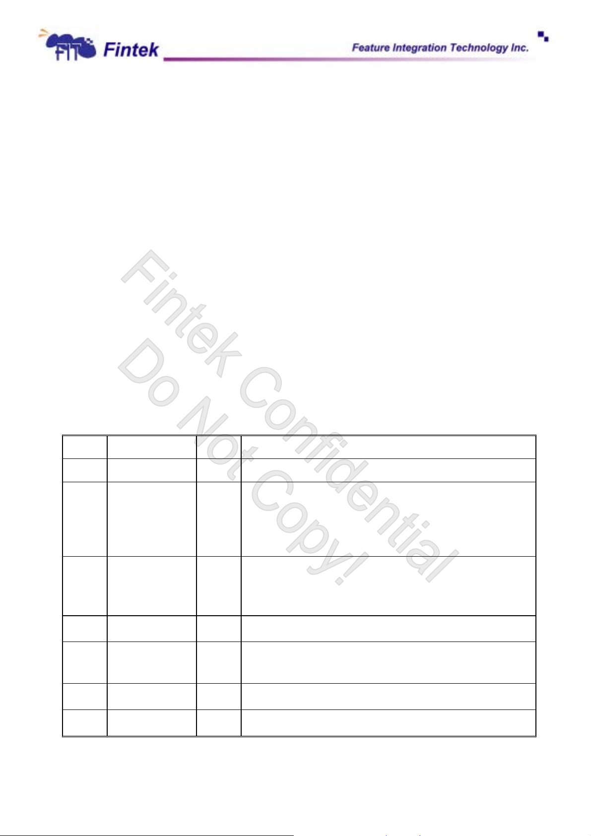
4. Pin Description
F81216D
I/O
8t5V-d100
- TTL level bi-directional pin with 8 mA source-sink capability, 5V tolerance, pull-down
100K ohms
I/O
- TTL level bi-directional pin with 12 mA source-sink capability
12t
I/OD
12
PCI5V - bi-direction pin, slew rate control, 5V tolerance.
OUT
12
OD
- Open-drain output pin with 12 mA sink capability
12
IN
- TTL level input pin
t
IN
- TTL level input pin and 5V tolerance.
t5V
IN
- TTL level input pin and schmitt trigger
ts
IN
ts5V
- TTL level input pin and Schmitt trigger, 5V tolerance.
- TTL level bi-directional pin, Open-drain outpu with 12 mA sink capability
- Output pin with 12 mA source-sink capability
P - Power
4.1 ISA/LPC Interface
Pin No. Pin Name Ty pe Description
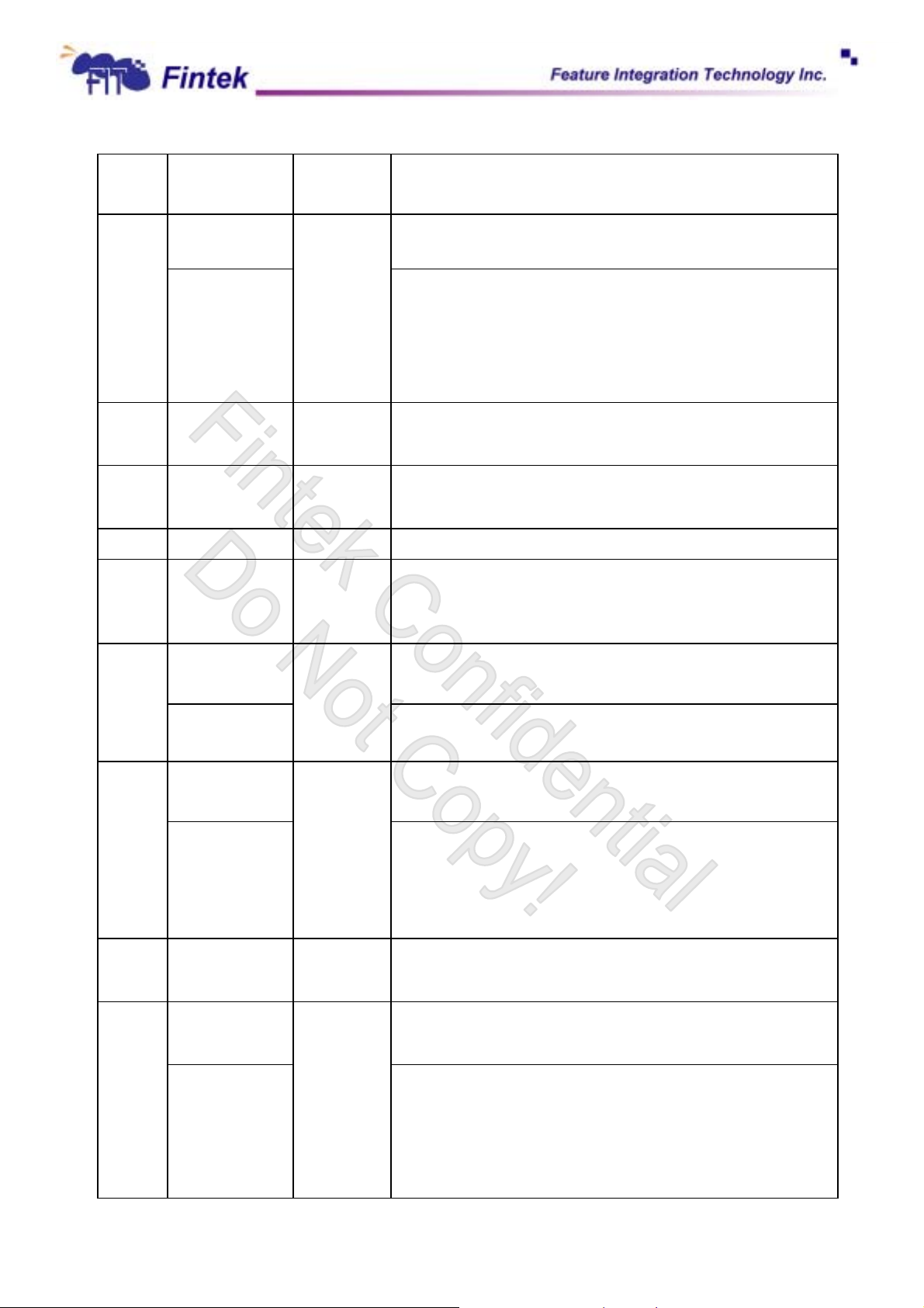
1 PCIRST# INts System PCI reset active low.
2 WDT_OUT# OD12 Watch dog timer output. When pin 24 power on setting
PS_WDT=0(default), Watch Dog timer time interval setting is
programmed by register. Once power on setting PS_WDT=1,
watch dog timer time interval will be fixed to 10 sec.
4~7 LPC_LAD[3:0]
8 LCLK IN
9 FRAME#
10 SERIRQ PCI5V In LPC mode, Serial IRQ input/Output.
12 CLKIN IN
PCI
IN
ts5V
ts5V
t5V
When in LPC mode, these signal lines communicate address,
5V
control, and data information over the LPC bus between a host
and a peripheral.
In LPC mode, this pin acts as PCI clock input.
In LPC mode, indicates start of a new cycle or termination of a
broken cycle.
Clock Input
-3-
July, 2004
V0.26P
Page 8
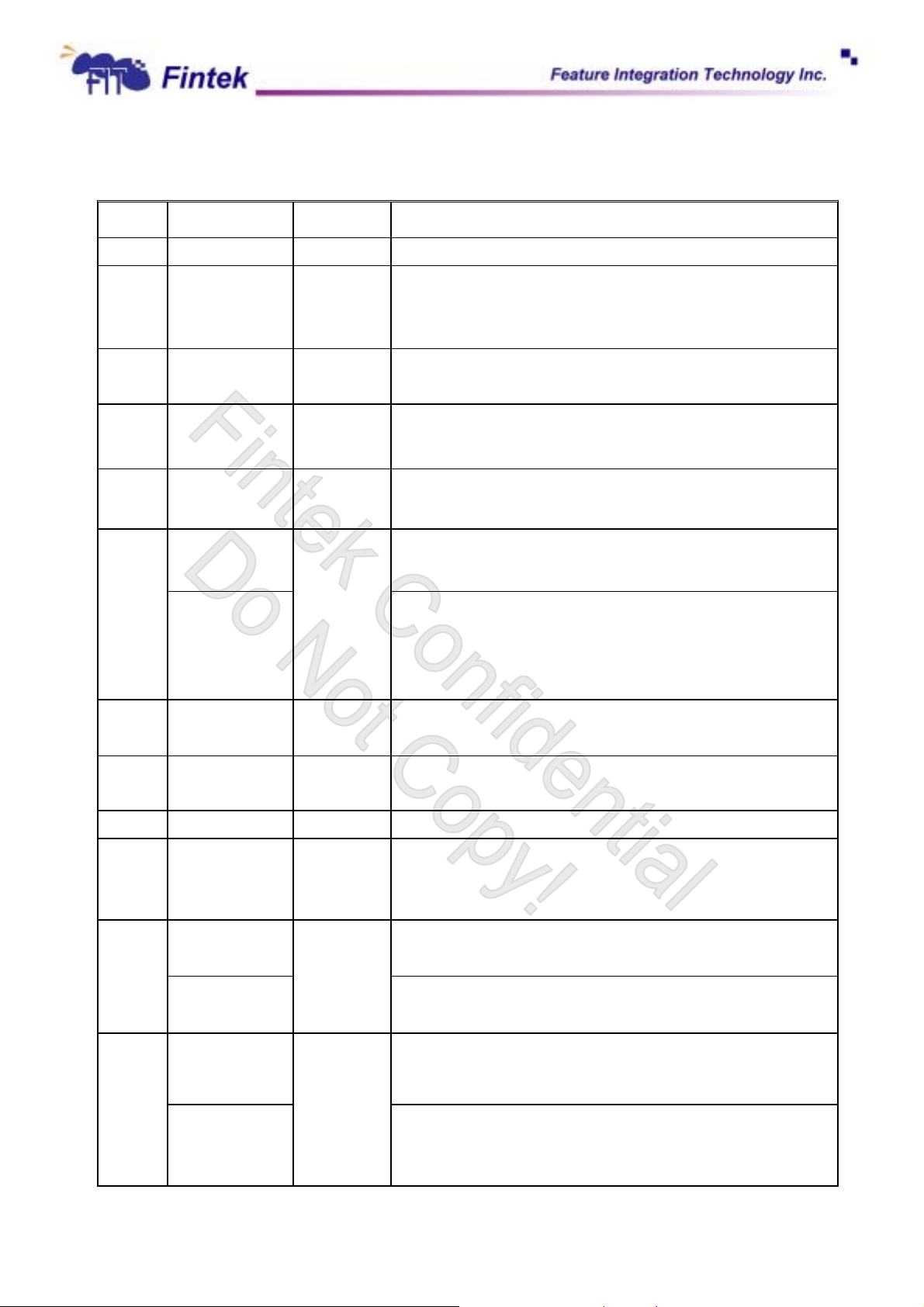
4.2 UART Interface
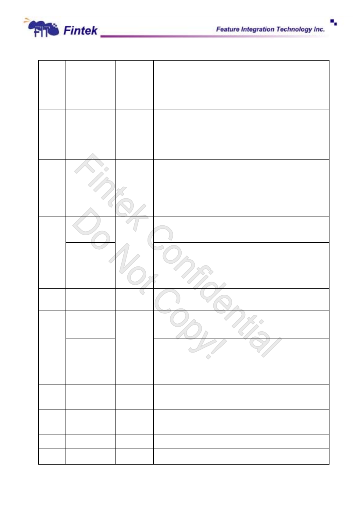
Pin No. Pin Name Ty pe Description
F81216D
13 CTS4# IN
14 DSR4# IN
15 RTS4# I/O
16 DTR4# I/O
17 SIN4 IN
18
SOUT4
PS_2E8_IRQD
I/O
Clear To Send is the modem control input.
t5V
Data Set Ready. An active low signal indicates the modem or
t5V
data set is ready to establish a communication link and transfer
data to the UART.
UART 4 Request To Send. An active low signal informs the
8t5V-d100
modem or data set that the controller is ready to send data.
UART 4 Data Terminal Ready. An active low signal informs
8t5V-d100
the modem or data set that controller is ready to communicate.
Serial Input. Used to receive serial data through the
t5V
communication link.
UART 4 Serial Output. Used to transmit serial data out to the
8t5V-d100
communication link.
Power setting pin to define the IRQD index.
Default PS_2E8_IRQD = 0, IRQF index is programmed by
register.
If PS_2E8_IRQD = 1, setting IRQF index to 0x2E8.
19 DCD4# IN
20 RI4# IN
21 CTS3# IN
22 DSR3# IN
23
RTS3#
I/O
PS_CONF_KE
Y0
24
DTR3#
I/O
PS_WDT
Data Carrier Detect. An active low signal indicates the
t5V
modem or data set has detected a data carrie r.
Ring Indicator. An active low signal indicates that a ring
t5V
signal is being received from the modem or data set.
Clear To Send is the modem control input.
t5V
Data Set Ready. An active low signal indicates the modem or
t5V
data set is ready to establish a communication link and transfer
8t5V-d100
data to the UART.
UART 3 Request To Send. An active low signal informs the
modem or data set that the controller is ready to send data.
Power on configuration setting pin. As for detail description,
please refer to register description.
UART 3 Data Terminal Ready. An active low signal informs
8t5V-d100
the modem or data set that controller is ready to communicate.
Power on setting pin to enable the watch dog timer.
Default PS_WDT=0, WDT time programmed by register.
When PS_WDT=1, WDT time is defined as 10 sec.
-4-
July, 2004
V0.26P
Page 9
F81216D
25 SIN3 IN
26
SOUT3
I/O
PS_3E8_IRQC
27 DCD3# IN
28 RI3# IN
31 CTS2# IN
32 DSR2# IN
Serial Input. Used to receive serial data through the
t5V
communication link.
UART 3 Serial Output. Used to transmit serial data out to the
8t5V-d100
communication link.
Power setting pin to define the IRQC index.
Default PS_3E8_IRQC = 0, IRQF index is programmed by
register.
If PS_3E8_IRQC = 1, setting IRQC index to 0x3E8.
Data Carrier Detect. An active low signal indicates the
t5V
modem or data set has detected a data carrie r.
Ring Indicator. An active low signal indicates that a ring
t5V
signal is being received from the modem or data set.
Clear To Send is the modem control input.
t5V
Data Set Ready. An active low signal indicates the modem or
t5V
data set is ready to establish a communication link and transfer
33
RTS2#
I/O
PS_CONF_KE
Y1
34
DTR2#
I/O
PS_2E0_IRQB
35 SIN2 IN
36
SOUT2 UART 2 Serial Output. Used to transmit serial data out to the
I/O
data to the UART.
UART 2 Request To Send. An active low signal informs the
8t5V-d100
modem or data set that the controller is ready to send data.
Power on configuration setting pin. As for detail description,
please refer to register description.
UART 2 Data Terminal Ready. An active low signal informs
8t5V-d100
the modem or data set that controller is ready to communicate.
Power setting pin to define the IRQB index.
Default PS_2E0_IRQB = 0, IRQB index is programmed by
register.
If PS_2E0_IRQB = 1, setting IRQB index to 0x2E0.
Serial Input. Used to receive serial data through the
t5V
communication link.
8t5V-d100
communication link.
PS_2F8_IRQB
Power setting pin to define the IRQB index.
Default PS_2F8_IRQB = 0, IRQB index is programmed by
register.
If PS_2F8_IRQB = 1, setting IRQB index to 0x2F8.
-5-
July, 2004
V0.26P
Page 10
F81216D
37 DCD2# IN
38 RI2# IN
39 CTS1# IN
40 DSR1# IN
41
RTS1#
I/O
PS_CONF_2E
42
DTR1#
I/O
Data Carrier Detect. An active low signal indicates the
t5V
modem or data set has detected a data carrie r.
Ring Indicator. An active low signal indicates that a ring
t5V
signal is being received from the modem or data set.
Clear To Send is the modem control input.
t5V
Data Set Ready. An active low signal indicates the modem or
t5V
data set is ready to establish a communication link and transfer
data to the UART.
UART 1 Request To Send. An active low signal informs the
8t5V-d100
modem or data set that the controller is ready to send data.
Power on configuration setting. Default PS_CONF_2E = 0,
setting the configuration to 0x4E. If PS_CONF_2E =1, setting
the configuration to 0x2E.
UART 1 Data Terminal Ready. An active low signal informs
8t5V-d100
the modem or data set that controller is ready to communicate.
PS_3E0_IRQA
43
44
SIN1 IN
SOUT1
I/O
PS_3F8_IRQA
45 DCD1# IN
46 RI1# IN
Power setting pin to define the IRQA index.
Default PS_3E0_IRQA = 0, IRQB index is programmed by
register.
If PS_3E0_IRQA = 1, setting IRQA index to 0x3E0.
Serial Input. Used to receive serial data through the
t5T
communication link.
UART 1 Serial Output. Used to transmit serial data out to the
8t5T-d100
communication link.
Power setting pin to define the IRQA index.
Default PS_3F8_IRQA = 0, IRQA index is programmed by
register.
If PS_3F8_IRQA = 1, setting IRQA index to 0x3F8.
Data Carrier Detect. An active low signal indicates the
t5T
modem or data set has detected a data carrie r.
Ring Indicator. An active low signal indicates that a ring
t5T
signal is being received from the modem or data set.
47 IRRX1 IN
Infrared Receiver input.
ts5T
48 IRTX1 OUT12 Infrared Transmitter Output.
-6-
July, 2004
V0.26P
Page 11

F81216D
4.3 Power
Pin No. Pin Name Ty pe Description
11,30 VCC P 3.3V power supply.
3, 29 GND P Ground.
-7-
July, 2004
V0.26P
Page 12

F81216D
5. Functional Description
The F81216D totally provides 4 UART ports through LPC interface. Among 4 UART
ports, one ports can support serial infrared communication. Besides, each UART includes
16-byte send/receive FIFO, a programmable baud rate generator, completed modem control
capability and interrupt system.
One watch dog timer is provided for system controlling and the time interval can be
programmed by register or hardware power on setting pin.
This IC needs one clock 24/48MHz input, and default is 24MHz. Powered by 3.3V voltage, the
F81216D is in 48 pin LQFP
5.1 LPC Interface
The F81216D can support LPC interface serving as a bus interface between host
(chipset) and peripheral (I/O chip) by hardware trapping. This interface provides much
less pins and more efficient transmission. Data transfer on the LPC bus is serialized over a
4 bit bus. The general characteristics of the interface implemented in F81216D are listed a s
below:
One control line, namely LPC_FRAME#, which is used by the host to start or stop
transfers. No peripherals drive this signal.
The LPC_LAD[3:0] bus, which communicates information serially. The information
conveyed is cycle type, cycle direction, chip selection, address, data, and wait states.
PCIRST# is an active low reset signal.
An additional 33 MHz PCI clock is needed in the F81216D for synchronization.
Interrupt requests are issued through LPC_SERIRQ.
Power management events are issued through PME#.
5.2 UART
-8-
July, 2004
V0.26P
Page 13
F81216D
A Universal Asynchronous Receiver/Transmitter (UART) is used to implement serial
communication. The F81216D incorporates four fully function UART compatible with NS16550D.
The UART ports perform serial to parallel conversion on receiving characters and parallel to
serial conversion on transmitting characters. The controllable characteristics of the data
transmission are baud rate, number of information bits per character, type of parity checking,
number of stop bits and breaking the transmission. The serial format is a start bit, followed by
five to eight data bits, a parity bit(if programmable), and one, one and half, or two stop bits. The
UART also includes completed modem control capability and interrupt system that may be
software trailed to the computing time required to handle the communication link. The UART
also has a FIFO mode to reduce the number of interrupts presented to the CPU. In the UART,
there is 16-byte FIFO for both receive and transmit mode.
5.2.1 UART Port Register
5.2.1.1 Receiver Buffer Register – Base + 0
Power-on default [7:0] = 0x00h.
Bit Name R/W Description
7:0 RBR[7:0] R The data received .
5.2.1.2 Transmitter Holding Register – Base + 0
Read only when LCR[7] is 0
Power-on default [7:0] = 0x00h.
Bit Name R/W Description
7:0 THR[7:0] W Data to be transmitted.
Write only when LCR[7] is 0
5.2.1.3 Divisor Latch ( LS ) – Base + 0
Power-on default [7:0] = 0x01h.
Bit Name R/W Description
7:0 DLL[7:0] R/W Baud generator divisor low byte.
Access only when LCR[7] is 1.
-9-
July, 2004
V0.26P
Page 14
5.2.1.4 Divisor Latch ( MS ) – Base + 1
Power-on default [7:0] = 0x00h.
Bit Name R/W Description
7:0 DLM[7:0] R/W Baud generator divisor high byte.
Access only when LCR[7] is 1.
F81216D
5.2.1.5 Interrupt Enable Register – Base + 1
Power-on default [7:0] = 0x00h.
Bit Name R/W Description
7:4 Reserved R/W Return 0 when read. Access only when LCR[7] is 0
3 EDSSI R/W Enable Modem Status Interrupt. Access only when LCR[7] is 0.
2 ELSI R/W Enable Line Status Error Interrupt. Access only when LCR[7] is 0.
1 ETBFI R/W Enable Transmitter Holding Register Empty Interrupt. Access only
0 ERBFI R/W Enable Received Data Availabl e Interrupt. Access only when LCR[7]
when LCR[7] is 0.
is 0
5.2.1.6 Interrupt Identification Register – Base + 2
Power-on default [7:0] = 0x01h.
Bit Name R/W Description
7 FIFO_EN R 0 : FIFO is disabled
1 : FIFO is enabled.
6 FIFO_EN R 0 : FIFO is disabled.
1 : FIFO is enabled.
5:4 Reserved R Return 0 when read.
3:1 IRQ_ID[2:0] R 000 : Interrupt is caused by Modem Status
001 : Interrupt is caused by Transmitter Holding Register Empty
010 : Interrupt is caused by Received Data Available.
110 : Interrupt is caused by Character Timeout
011 : Interrupt is caused by Line Status..
0 IRQ_PENDN R 1 : Interrupt is not pending.
0 : Interrupt is pending.
-10-
July, 2004
V0.26P
Page 15
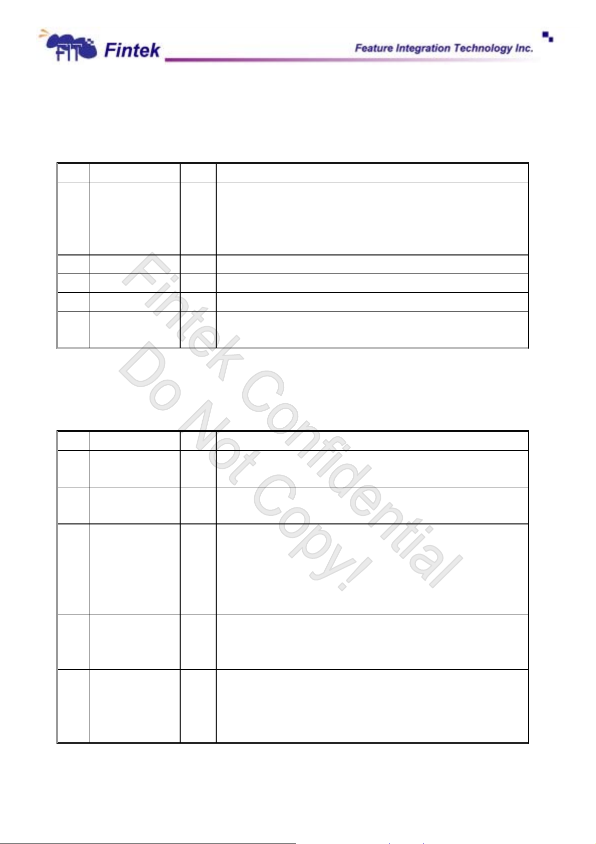
5.2.1.7 FIFO Control Register – Base + 2
Power-on default [7:0] = 0x00h.
Bit Name R/W Description
7:6 RCVR_TRIG[1:0] W 00 : Receiver FIFO trigger level is 1.
01 : Receiver FIFO trigger level is 4.
10 : Receiver FIFO trigger level is 8.
5:3 Reserved W
11 : Receiver FIFO trigger level is 14.
F81216D
2 CLRTX W 1 : Reset the transmitter FIFO.
1 CLRRX W 1 : Reset the receiver FIFO.
0 FIFO_EN W 0 : Disable FIFO
1 : Enable FIFO
5.2.1.8 Line Control Register – Base + 3
Power-on default [7:0] = 0x00h.
Bit Name R/W Description
7 DLAB R/W 0 : Divisor Latch can’t be accessed.
1 : Divisor Latch can be accessed via Base and Base+1.
6 SETBRK R/W 1 : Transmit a break condition.
0 : Transmitter is in normal condition.
5:3 STKPAR
EPS
PEN
R/W XX0 : Parity Bit is disable
001 : Parity Bit is odd.
011 : Parity Bit is even
101 : Parity Bit is logic 1
111 : Parity Bit is logic 0
2 STB R/W 0 : St op bit is one bit
1 : When word length is 5 bit stop bit is 1.5 bit
else stop bit is 2 bit
1:0 WLS[1:0] R/W 00 : Word length is 5 bit
01 : Word length is 6 bit
10 : Word length is 7 bit
11 : Word length is 8 bit
-11-
July, 2004
V0.26P
Page 16
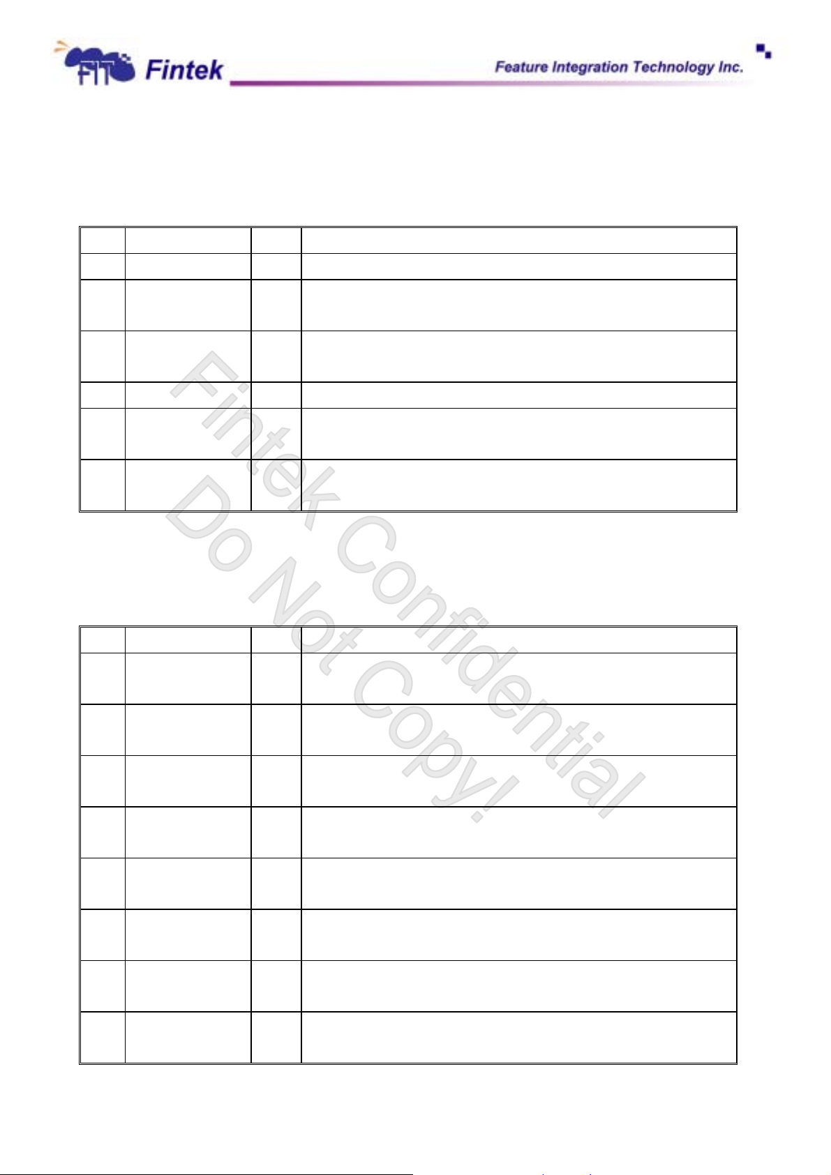
5.2.1.9 MODEM Control Register – Base + 4
Power-on default [7:0] = 0x00h.
Bit Name R/W Description
7:5 Reserved R/W Return 0 when read.
4 LOOP R/W 0 : UART in normal condition.
F81216D
3 OUT2 R/W 0 : All interrupt is disable.
2 OUT1 R/W Read from MSR[6] is loop back mode
1 : UART is internal loop back
1 : Interrupt is enabled/disabled by IER.
1 RTS R/W 0 : RTS# is forced to logic 1
1 : RTS# is forced to logic 0
0 DTR R/W 0 : DTR# is forced to logic 1
1 : DTR# is forced to logic 0
5.2.1.10 Line Status Register – Base + 5
Power-on default [7:0] = 0x60h.
Bit Name R/W Description
7 RCR_ERR R 0 : No error in the FIFO when FIFO is enabled
1 : Error in the FIFO when FIFO is enabled.
6 TEMT R 0 : Transmitter is in transmitting.
1 : Transmitter is empty.
5 THRE R 0 : Transmitter Holding Register is not empty.
1 : Transmitter Holding Register is empty.
4 BI R 0 : No break condition detected.
1 : A break condition is detected.
3 FE R 0 : Data received has no frame error.
1 : Data received has frame error.
2 PE R 0 : Data received has no parity error.
1 : Data received has parity error.
1 OE R 0 : No overrun condition occur.
1 : A overrun condition occur.
0 DR R 0 : No data is ready for read.
1 : Data is received .
-12-
July, 2004
V0.26P
Page 17
F81216D
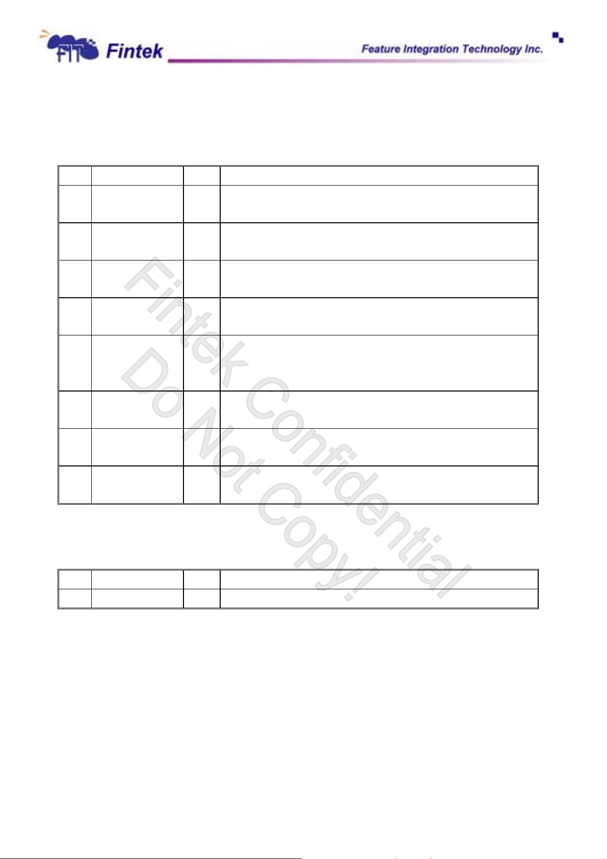
5.2.1.11 MODEM Status Register – Base + 6
Power-on default [7:0] = 0xX0h.
Bit Name R/W Description
7 DCD R Complement of DCD# input. In loop back mode, this bit is equivalent
to OUT2 in MCR.
6 RI R Complement of RI# input. In loop back mode , this bit is equivalent to
5 DSR R Complement of DSR# input. In loop back mode , this bit is
OUT1 in MCR
equivalent to DTR in MCR
4 CTS R Complement of CTS# input. In loop back mode , this bit is equivalent
to RTS in MCR
3 DDCD R 0 : No state changed at DCD#.
1 : State chan ged at DCD#.
2 TERI R 0 : No Trailing edge at RI#.
1 : A low to high transition at RI#.
1 DDSR R 0 : No state changed at DSR#.
1 : State changed at DSR#.
0 DCTS R 0 : No state changed at CTS#.
1 : State changed at CTS#.
5.2.1.11 Scratch Register – Base + 7
Power-on default [7:0] = 0x00h.
Bit Name R/W Description
7:0 SCR_DATA[7:0] R/W Scratch register.
5.3 IR Function
The F81216D infrared interface provides a two way wireless communications port using
infrared as the transmission medium. The IrDA 1.0 (SIR) is found in UART1 IrDA SIR specifies
asynchronous serial communication at baud rate up to 115.2Kbps. Each byte is sent serial LSB first
beginning with a zero value start bit. A zero is signaled by sending a single infrared pulse at the
beginning of the serial bit time. A one is signaled by the absence of an infrared pulse during the bit
time. IRTX acts as a transmit pin and IRRX acts as a receiving one. As for detail description, please
refer to register description.
-13-
July, 2004
V0.26P
Page 18
F81216D
5.4 Watch Dog Timer Function
Watch dog timer is provided for system controlling. If time-out can trigger one signal to low
level, the signal default is tri-state (need external pull up resister).
The time interval has three ways:
One is the hardware power on setting to enable, timer set to 10 second (24MHz). If 48MHz
clock input, the timer is set to 5 second.
Two is programmed by registers.
The other is set the base address into registers, and use the base address the control it.
The timer unit has three kinds: 10mS, 1S, 1Min.
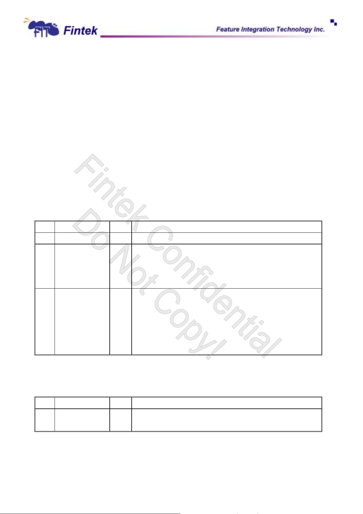
5.4.1 Watchdog Port Register
5.4.1.1 Timer Status and Control Register – Base + 0
Power-on default [7:0] = 0x02 when DTR3#/PS_WDT is pull-up, else 0x0.
Bit Name R/W Description
7:3 Reserved R/W Return 0 when read.
2:1 WDT_UNIT[1:0] R/W 00 : Timer Unit is 10ms.
01 : Timer Unit is 1 second
10 : Timer Unit is 1 minute.
11 : reserved.
0 WDT_EVENT R/W When read
0 : no time out occur.
1 : time out has occurred.
when write
0 : no action
1 : clear the time out status.
5.4.1.2 Timer Count Number Register – Base + 1
Power-on default [7:0] = 0x0Ah when DTR3#/PS_WDT is pull-up , else 0x00h.
Bit Name R/W Description
7:0 WDT_CNT[7:0] R/W The number of count for watchdog timer.
Write the same value to enable the timer, write 0 to disable timer.
-14-
July, 2004
V0.26P
Page 19

F81216D
5.5 Serial IRQ
F81216D supports a serial IRQ scheme. Because more than one device may need to share
the signal serial IRQ signal line, an open drain signal scheme is used. The clock source is the PCI
clock. The serial interrupt is transferred on the SERIRQ signal, one cycle consisting of three
frames types: a start frame, several IRQ/Data frame, and one Stop frame.
5.5.1 Start Frame
mode. In the Quiet mode, the peripheral drives the SERIRQ signal active low for one clock, and
then tri-states it. This brings all the states machines of the peripherals from idle to active states.
The host controller will then take over driving SERIRQ signal low in the next clock and will continue
driving the SERIRQ low for programmable 3 to 7 clock periods. This makes the total number of
There are two modes of operation for the SERIRQ Start frame: Quiet mode and Continuous
clocks low for 4 to 8 clock periods. After these clocks, the host controller will drive the SERIRQ high
for one clock and then tri-states it. In the Continuous mode, only the host controller initiates the
START frame to update IRQ/Data line information. The host controller drives the SERIRQ signal
low for 4 to 8 clock periods. Upon a reset, the SERIRQ signal is defaulted to the Continuous mode
for the host controller to initiate the first Start frame.
5.5.2 IRQ/Data Frame
Once the start frame has been initiated, all the peripherals must start counting frames based
on the rising edge of the start pulse. Each IRQ/Data Frame is three clocks: Sample phase,
Recovery phase, and Turn-around phase. During the Sample phase, the peripheral drives SERIRQ
low if the corresponding IRQ is active. If the corresponding IRQ is inactive, then SERIRQ must be
left tri-stated. During the Recovery phase, the peripheral device drives the SERIRQ high. During
the Turn-around phase, the peripheral device left the SERIRQ tri-stated. The IRQ/Da ta Frame has
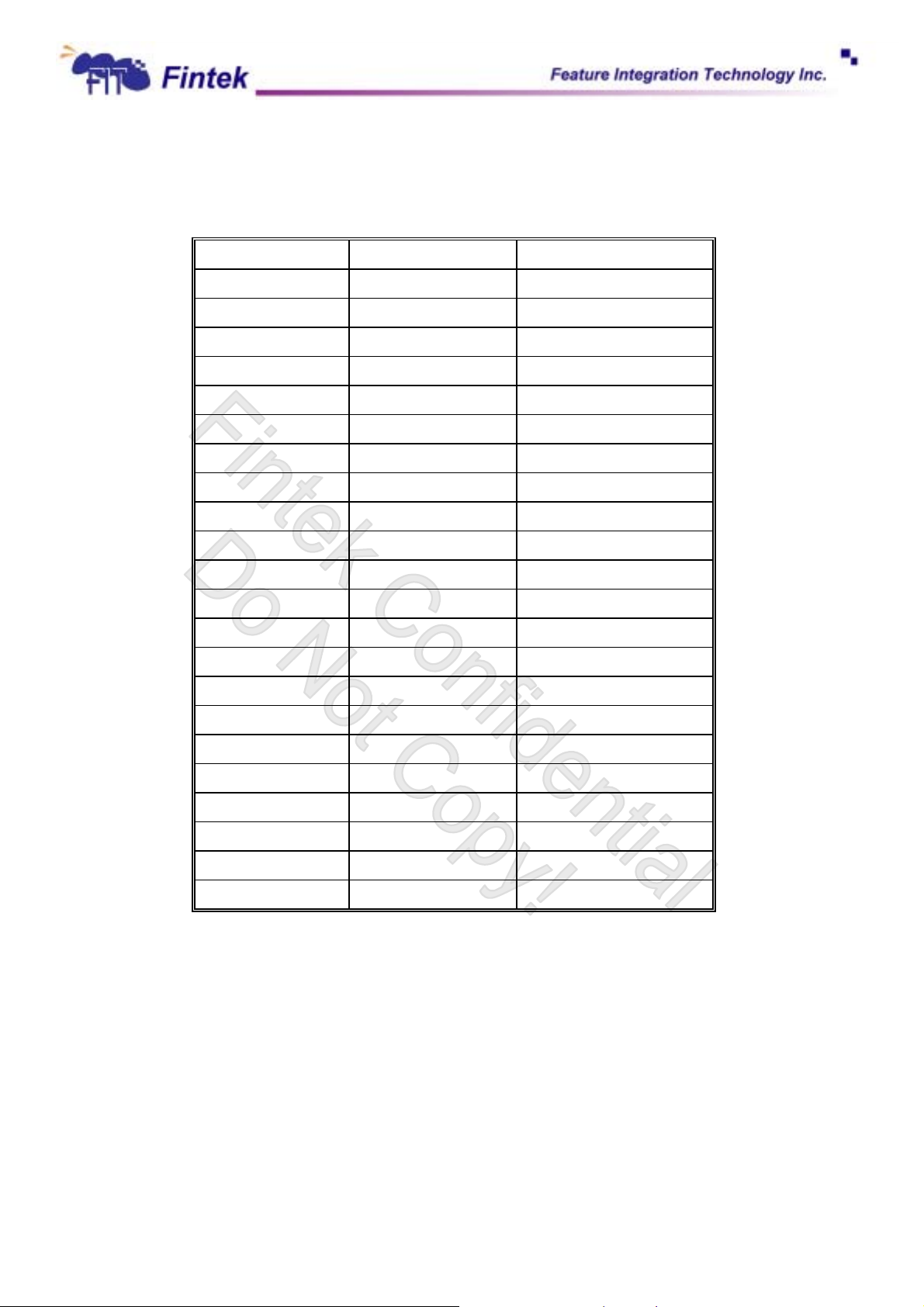
a number of specific order, as shown in Table 5-1. The F81216D is only support IRQ3, IRQ4, IRQ5,
IRQ9, IRQ10, and IRQ11.
-15-
July, 2004
V0.26P
Page 20
F81216D
Table 5-1 IRQSER Sampling periods
IRQ/Data Frame Signal Sampled # of clocks past Start
1 IRQ0 2
2 IRQ1 5
3 SMI#
8
4 IRQ3 11
5 IRQ4 14
6 IRQ5 17
7 IRQ6 20
8 IRQ7 23
9 IRQ8 26
10 IRQ9 29
11 IRQ10 32
12 IRQ11 35
13 IRQ12 38
14 IRQ13 41
15 IRQ14 44
16 IRQ15 47
17 IOCHCK#
18 INTA#
19 INTB#
20 INTC#
21 INTD#
50
53
56
59
62
32:22 Unassigned 95
5.5.3 Stop Frame
After all IRQ/Data Frames have completed, the host controller will terminate SERIRQ by
a Stop frame. Only the host controller can initiate the Stop frame by driving SERIRQ low for 2 or 3
clocks. If the Stop Frame is low for 2 clocks, the next SERIRQ cycle's Sample mode is the Quiet
mode. If the Stop Frame is low for 3 clocks, the next SERIRQ cycle's Sample mode is the
Continuous mode.
-16-
July, 2004
V0.26P
Page 21
F81216D
6. Register Description
Registers are programmed by port 0x4E and 0x4F. 0x4E is the index port and 0x4F is the data port .
To enable configuration registers programming, entry key must output twice to index port
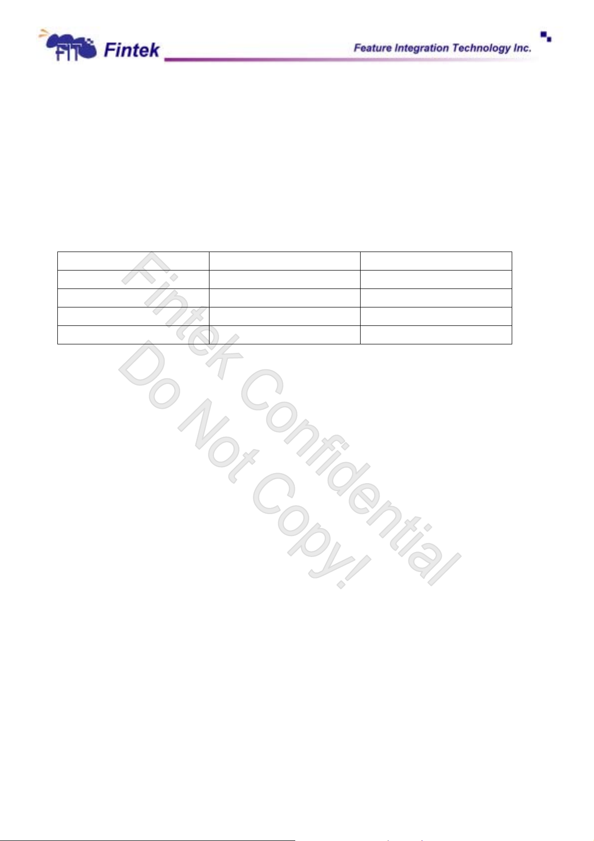
continuously. The entry key is decided by power on setting pins RTS2#/PS_CONF_KEY1 and
RTS3#/PS_CONF_KEY0 as following:
RTS2#/PS_CONF_KEY1 RTS3#/PS_CONF_KEY0 Entry key
0 0 0x77 ( default )
0 1 0xA0
1 0 0x87
1 1 0x67
To exit configuration registers programming, output 0xAA to index port.
Sample code for configuration:
1. Clock in used 48MHz, UART 1~6 address (0x3f8, 0x2f8, 0x3e8, 0x2e8,IRQ(3, 4, 5 ,9, Entry
key is 0x77:
outportb(0x4e, 0x77);
outportb(0x4e, 0x77); //Entry configuration mode
outportb(0x4e, 0x25); //Select register index 0x25
outportb(0x4f, 0x01); //Set bit 0 to 1 select clock input to 48MHz
outportb(0x4e, 0x07); //Select register index 0x07
outportb(0x4f, 0x00); //Select LDN 0
outportb(0x4e, 0x60); //Select LDN 0 register index 0x60
outportb(0x4f, 0x03); //Set UART 1 base address high byte to 0x03
outportb(0x4e, 0x61); //Select LDN 0 register index 0x61
outportb(0x4f, 0xf8); //Set UART 1 base address low byte to 0xf8
outportb(0x4e, 0x70); //Select LDN 0 register index 0x70
outportb(0x4f, 0x03); //Set UART 1 interrupt channel to IRQ 3
outportb(0x4e, 0x30); //Select LDN 0 register index 0x30
outportb(0x4f, 0x01); //Enable UART 1
outportb(0x4e, 0x07); //Select register index 0x07
outportb(0x4f, 0x01); //Select LDN 1
outportb(0x4e, 0x60); //Select LDN 1 register index 0x60
-17-
July, 2004
V0.26P
Page 22

outportb(0x4f, 0x02); //Set UART 2 base address high byte to 0x02
outportb(0x4e, 0x61); //Select LDN 1 register index 0x61
outportb(0x4f, 0xf8); //Set UART 2 base address low byte to 0xf8
outportb(0x4e, 0x70); //Select LDN 1 register index 0x70
outportb(0x4f, 0x04); //Set UART 2 interrupt channel to IRQ 4
outportb(0x4e, 0x30); //Select LDN 1 register index 0x30
outportb(0x4f, 0x01); //Enable UART 2
outportb(0x4e, 0x07); //Select register index 0x07
outportb(0x4f, 0x02); //Select LDN 2
F81216D
outportb(0x4e, 0x60); //Select LDN 2 register index 0x60
outportb(0x4f, 0x03); //Set UART 3 base address high byte to 0x03
outportb(0x4e, 0x61); //Select LDN 2 register index 0x61
outportb(0x4f, 0xe8); //Set UART 3 base address low byte to 0xe8
outportb(0x4e, 0x70); //Select LDN 2 register index 0x70
outportb(0x4f, 0x05); //Set UART 3 interrupt channel to IRQ 5
outportb(0x4e, 0x30); //Select LDN 2 register index 0x30
outportb(0x4f, 0x01); //Enable UART 3
outportb(0x4e, 0x07); //Select register index 0x07
outportb(0x4f, 0x03); //Select LDN 3
outportb(0x4e, 0x60); //Select LDN 3 register index 0x60
outportb(0x4f, 0x02); //Set UART 4 base address high byte to 0x02
outportb(0x4e, 0x61); //Select LDN 3 register index 0x61
outportb(0x4f, 0xe8); //Set UART 4 base address low byte to 0xe8
outportb(0x4e, 0x70); //Select LDN 3 register index 0x70
outportb(0x4f, 0x09); //Set UART 4 interrupt channel to IRQ 9
outportb(0x4e, 0x30); //Select LDN 3 register index 0x30
outportb(0x4f, 0x01); //Enable UART 4
outportb(0x4e, 0xaa); //Exit configuration mode
2. Set Watch Dog timer base address 0x300~0x301:
outportb(0x4e, 0x77);
outportb(0x4e, 0x77); //Entry configuration mode
outportb(0x4e, 0x07); //Select register index 0x07
outportb(0x4f, 0x08); //Select LDN 8
outportb(0x4e, 0x60); //Select LDN 8 register index 0x60
-18-
July, 2004
V0.26P
Page 23
F81216D
outportb(0x4f, 0x03); //Set Watch Dog timer base address high byte to 0x03
outportb(0x4e, 0x61); //Select LDN 8 register index 0x61
outportb(0x4f, 0x00); //Set Watch Dog Timer base address low byte to 0x00
outportb(0x4e, 0x30); //Select LDN 8 register index 0x30
outportb(0x4f, 0x01); //Enable Watch Dog Timer Device
outportb(0x4e, 0xaa); //Exit configuration mode
3. Set Watch Dog timer to 20 second used base address 0x300~0x301:
outportb(0x300, 0x03); //Select unit to one second and clear time out status
outportb(0x301, 0x14);
outportb(0x301, 0x14); //Set timer to 20 second and enable timer
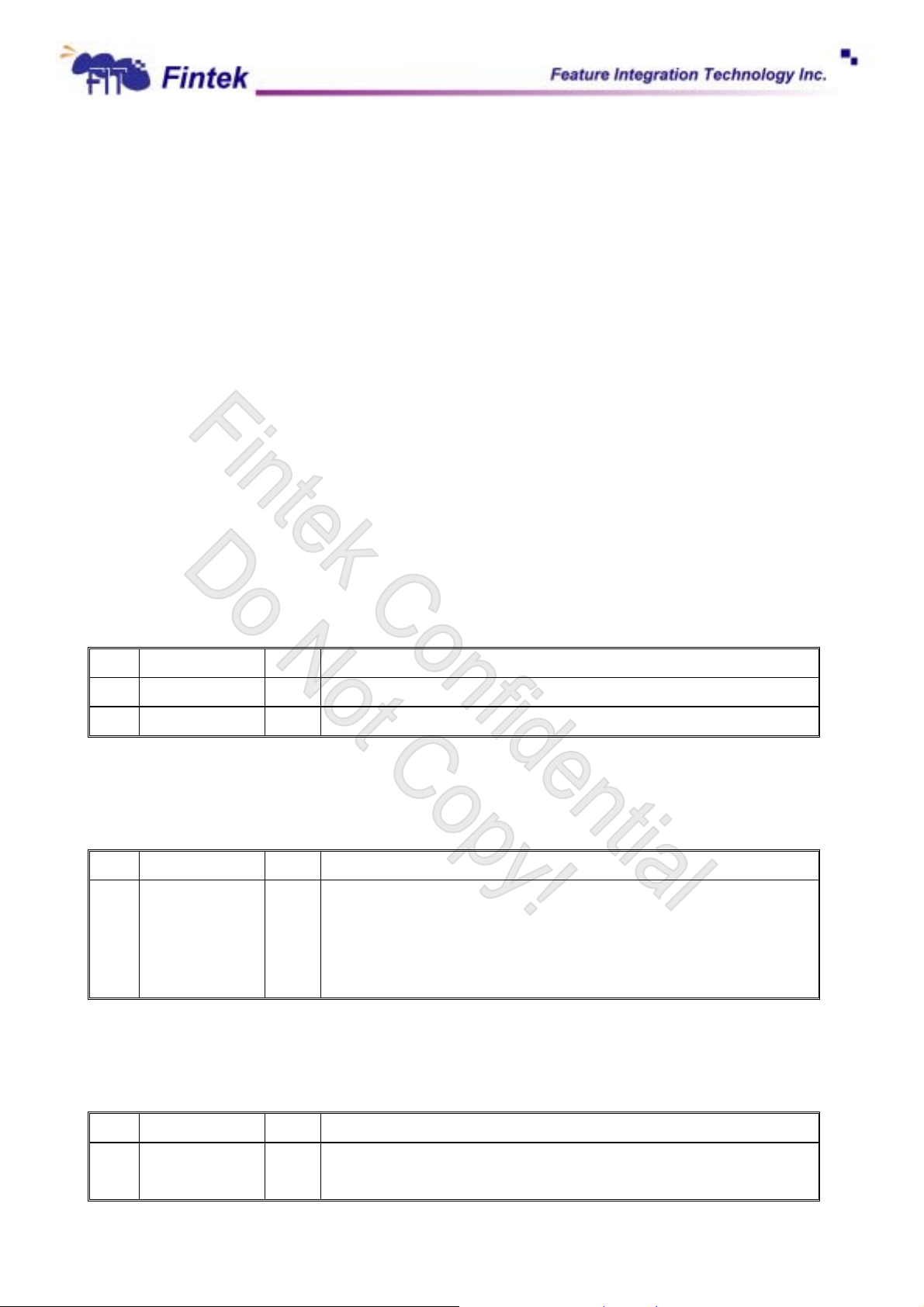
6.1 Global Control Register
6.1.1 Software Reset Register – index 02h
Power-on default [7:0] = 0x00h
Bit Name R/W Description
7:1 Reserved R/W Return 0 when read.
0 SWRST R/W Write 1 to reset configuration register. This bit is auto cleared.
6.1.2 Logic Device Select Register – index 07h
Power-on default [7:0] = 0x00h
Bit Name R/W Description
7:0 LDN[7:0] R/W 00h : Select UART 1 device configuration register
01h : Select UART 2 device configuration register
02h : Select UART 3 device configuration register
03h : Select UART 4 device configuration register
08h : Select Watchdog Timer device configuration register
6.1.3 Device ID Register– index 20h, 21h
Power-on default [7:0], 0x02h for index 20h, 0x08h for index 21h
Bit Name R/W Description
7:0 DEVID R Return 0208h when read index 20h and 21h respectively , indicate the
device ID.
-19-
July, 2004
V0.26P
Page 24
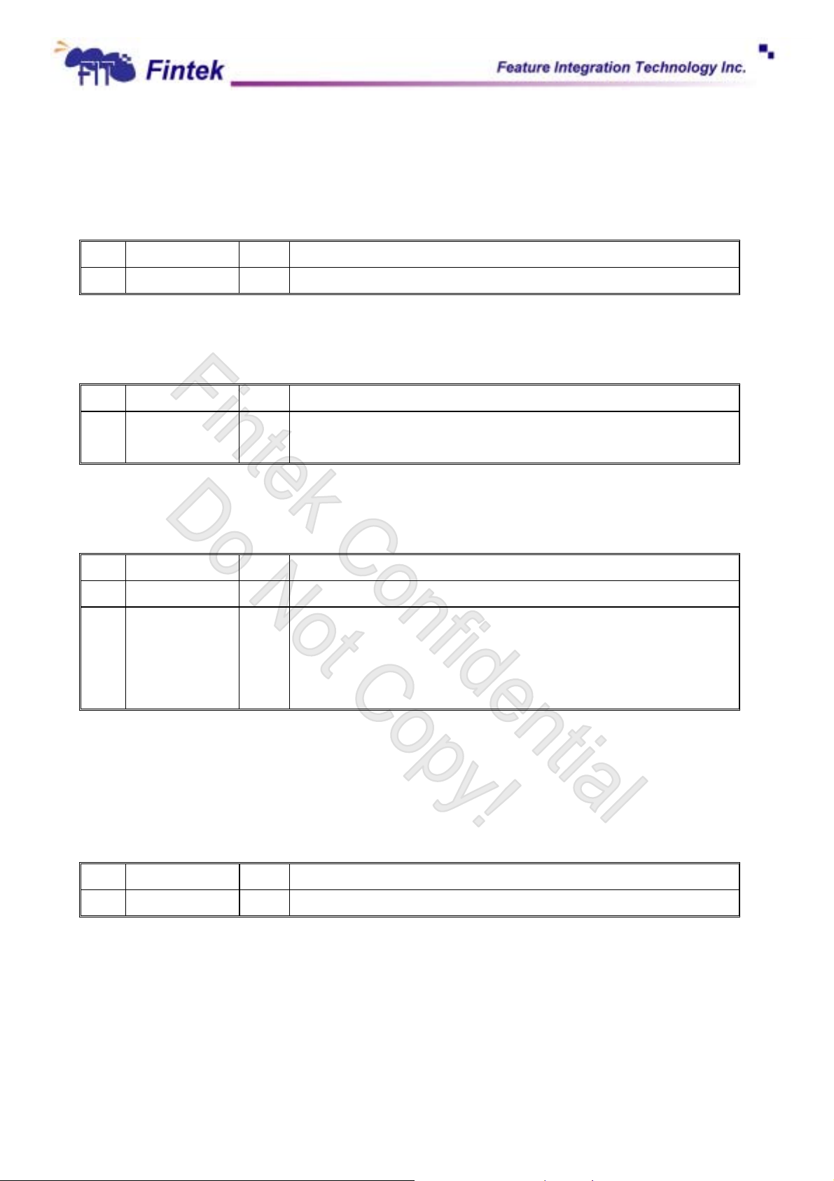
6.1.4 Device Reversion Register– index 22h
Power-on default [7:0], 0x01h
Bit Name R/W Description
7:0 DEVREV R Return 01h when read , indicate the device reversion.
6.1.5 Vendor ID Register– index 23h, 24h
Power-on default [7:0], 0x19h for index 23h, 0x34h for index 24h
F81216D
Bit Name R/W Description
7:0 VENDID R Return 1934h when read index 23h and 24h respectively, indicate the
6.1.6 Clock Source Select Register – index 25h
vendor ID of Fintek.
Power-on default [7:0], 0x00h
Bit Name R/W Description
7:1 Reserved R/W Return 0 when read.
0 CLK_SEL R/W 1 : The CLKIN is 48MHz
0 : The CLKIN is 24MHz.
This bit must program to indicate the frequency of the clock source, or
the device will not function correctly.
6.1.8 Test Mode Register – index 2Fh
Power-on default [7:0], 0000_0000b
Bit Name R/W Description
7:0 TESTMODE R/W Test mode register, reserved for Fintek use o nly.
-20-
July, 2004
V0.26P
Page 25
F81216D
6.2 UART 1 Device Control Register (LDN 0)
6.2.1 Device Enable Register – index 30h
Power-on default [7:0] = 0x01h when SOUT1/PS_3F8_IRQA or DTR1#/PS_3E0_IRQA is pull-up,
else 0x00h.
Bit Name R/W Description
7:1 Reserved R/W Return 0 when read.
0 URA_EN R/W 0 : Disable UART 1.
1 : Enable UART 1..
6.2.2 I/O Port Select Register – index 60h
Power-on default [7:0] = 0x03h when SOUT1/PS_3F8_IRQA or DTR1#/PS_3E0_IRQA is pullup,
else 0x00h.
Bit Name R/W Description
7:0 URA_BASE[15:8] R/W UART 1 I/O Port Address high byte.
6.2.3 I/O Port Select Register – index 61h
Power-on default [7:0] = 0xF8h when SOUT1/PS_3F8_IRQA is pull-up,
0xE0h when DTR1#/PS_3E0_IRQA is pull-up, else 0x00h.
Bit Name R/W Description
7:0 URA_BASE[7:0] R/W UART 1 I/O Port Address low byte.
6.2.4 IRQ Channel Select Register – index 70h
Power-on default [7:0] = 0x03h when SOUT1/PS_3F8_IRQA or DTR1#/PS_3E0_IRQA is pull-up,
else 0x00h
Bit Name R/W Description
7:6 Reserved R/W Return 0 when read.
5 URAIRQ_MODE R/W 0 : PCI IRQ sharing mode.
1 : ISA IRQ sharing mode.
This bit is effective in IRQ sharing mode.
4 URAIRQ_SHAR R/W 0 : IRQ is not sharing with other device.
1 : IRQ is sharing with other device.
3:0 SELURAIRQ[3:0] R/W Select the Serial IRQ channel.
-21-
July, 2004
V0.26P
Page 26
F81216D
6.2.5 UART 1 Clock Select Register – index F0h
Power-on default [7:0] = 0x00h.
Bit Name R/W Description
7:4 Reserved R/W Return 0 when read.
3 RXW4C_IRA R/W 0 : No reception delay when SIR is changed from TX to RX.
2 TXW4C_IRA R/W 0 : No transmission delay when SIR is changed from RX to TX.
1:0 SELURACLK1
SELURACLK0
R/W 00 : UART 1 clock source is 1.8462MHz ( 24MHz/13 )
1 : Reception delay 4 character-time when SIR is changed from TX
to RX.
1 : Transmission delay 4 character-time when SIR is changed from
RX to TX.
01 : UART 1 clock source is 18.462MHz ( 24MHz/1.3 )
10 : UART 1 clock source is 24MHz ( 24MHz/1 )
11 : UART 1 clock source is 14.769MHz ( 24MHz/1.625 )
6.2.6 IR1 Control Register – index F1h
Power-on default [7:0] = 0x44h.
Bit Name R/W Description
7:5 Reserved R/W Return 010b when read.
4:3 IRA_MODE1
IRA_MODE0
2 Reserved R/W Return 1 when read.
1 TXINV_IRA R/W 0 : IRTX1 is not inversed.
0 RXINV_IRA R/W 0 : IRRX1 is not inversed.
R/W 0X: Disable IR1 function.
10 : Enable IR1 function, active pulse is 1.6uS.
11 : Enable IR1 function, active pulse is 3/16 bit time.
1 : Inverse the IRTX1.
1 : Inverse the IRRX1.
-22-
July, 2004
V0.26P
Page 27
F81216D
6.3 UART 2 Device Control Register (LDN 1)
6.3.1 Device Enable Register – index 30h
Power-on default [7:0] = 0x01h when SOUT2/PS_2F8_IRQB or DTR2#/PS_2E0_IRQB is pull-up,
else 0x00h.
Bit Name R/W Description
7:1 Reserved R/W Return 0 when read.
0 URB_EN R/W 0 : Disable UART 2.
1 : Enable UART 2.
6.3.2 I/O Port Select Register – index 60h
Power-on default [7:0] = 0x02h when SOUT2/PS_2F8_IRQB or DTR2#/PS_2E0_IRQB is pullup,
else 0x00h.
Bit Name R/W Description
7:0 URB_BASE[15:8] R/W UART 2 I/O Port Address high byte.
6.3.3 I/O Port Select Register – index 61h
Power-on default [7:0] = 0xF8h when SOUT2/PS_2F8_IRQB is pull-up,
0xE0h when DTR2#/PS_2E0_IRQB is pull-up, else 0x00h.
Bit Name R/W Description
7:0 URB_BASE[7:0] R/W UART 2 I/O Port Address low byte.
6.3.4 IRQ Channel Select Register – index 70h
Power-on default [7:0] = 0x03h when SOUT2/PS_2F8_IRQB or DTR2#/PS_2E0_IRQB is pull-up,
else 0x00h
Bit Name R/W Description
7:6 Reserved R/W Return 0 when read.
5 URBIRQ_MODE R/W 0 : PCI IRQ sharing mode.
1 : ISA IRQ sharing mode.
This bit is effective in IRQ sharing mode.
4 URBIRQ_SHAR R/W 0 : IRQ is not sharing with other device.
1 : IRQ is sharing with other device.
-23-
July, 2004
V0.26P
Page 28
3:0 SELURAIRQ[3:0] R/W Select the Serial IRQ channel.
6.3.5 UART 2 Clock Select Register – index F0h
Power-on default [7:0] = 0x00h.
Bit Name R/W Description
7:2 Reserved R/W Return 0 when read.
1:0 SELURACLK1
SELURACLK0
R/W 00 : UART 2 clock source is 1.8462MHz ( 24MHz/13 )
01 : UART 2 clock source is 18.462MHz ( 24MHz/1.3 )
10 : UART 2 clock source is 24MHz ( 24MHz/1 )
11 : UART 2 clock source is 14.769MHz ( 24MHz/1.625 )
F81216D
6.4 UART 3 Device Control Register (LDN 2)
6.4.1 Device Enable Register – index 30h
Power-on default [7:0] = 0x01h when SOUT3/PS_3E8_IRQC is pull-up, else 0x00h.
Bit Name R/W Description
7:1 Reserved R/W Return 0 when read.
0 URC_EN R/W 0 : Disable UART 3.
1 : Enable UART 3.
6.4.2 I/O Port Select Register – index 60h
Power-on default [7:0] = 0x03h when SOUT3/PS_3E8_IRQC is pull-up, else 0x00h.
Bit Name R/W Description
7:0 URC_BASE[15:8] R/W UART 3 I/O Port Address high byte.
6.4.3 I/O Port Select Register – index 61h
Power-on default [7:0] = E8h when SOUT3/PS_3E8_IRQC is pull-up, else 0x00h.
Bit Name R/W Description
7:0 URC_BASE[7:0] R/W UART 3 I/O Port Address low byte.
-24-
July, 2004
V0.26P
Page 29
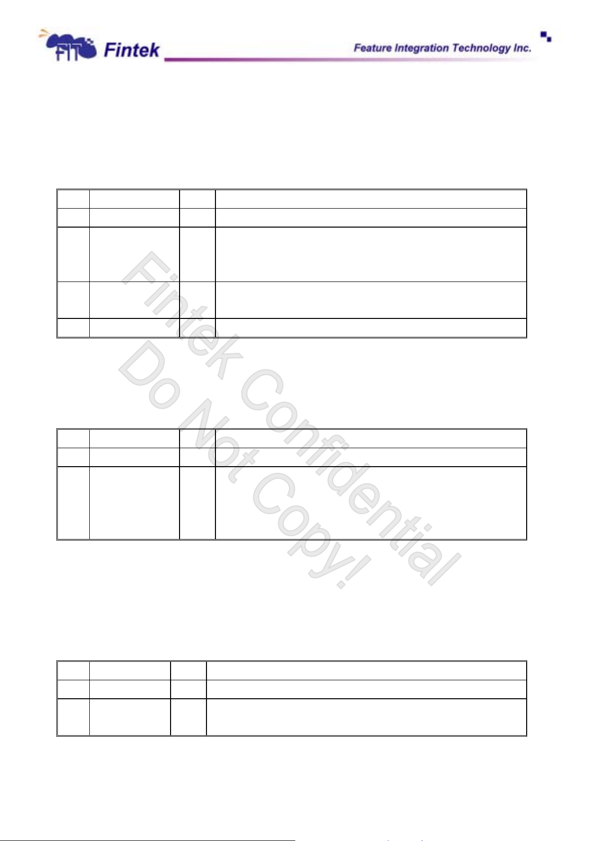
6.4.4 IRQ Channel Select Register – index 70h
Power-on default [7:0] = 0x05h when SOUT3/PS_3E8_IRQC is pull-up, else 0x00h.
Bit Name R/W Description
7:6 Reserved R/W Return 0 when read.
F81216D
5 URCIRQ_MODE R/W 0 : PCI IRQ sharing mode.
4 URCIRQ_SHAR R/W 0 : IRQ is not sharing with other device.
3:0 SELURCIRQ[3:0] R/W Select the Serial IRQ channel.
1 : ISA IRQ sharing mode.
This bit is effective in IRQ sharing mode.
1 : IRQ is sharing with other device.
6.4.5 UART 3 Clock Select Register – index F0h
Power-on default [7:0] = 0000_0000b.
Bit Name R/W Description
7:2 Reserved R/W Return 0 when read.
1:0 SELURCCLK1
SELURCCLK0
R/W 00b : UART 3 clock source is 1.8462MHz ( 24MHz/13 )
01b : UART 3 clock source is 18.462MHz ( 24MHz/1.3 )
10b : UART 3 clock source is 24MHz ( 24MHz/1 )
11b : UART 3 clock source is 14.769MHz ( 24MHz/1.625 )
6.5 UART 4 Device Control Register (LDN 3)
6.5.1 Device Enable Register – index 30h
Power-on default [7:0] = 0x01h when SOUT4/PS_2E8_IRQD is pull-up, else 0x00h.
Bit Name R/W Description
7:1 Reserved R/W Return 0 when read.
0 URD_EN R/W 0 : Disable UART 4.
1 : Enable UART 4.
-25-
July, 2004
V0.26P
Page 30
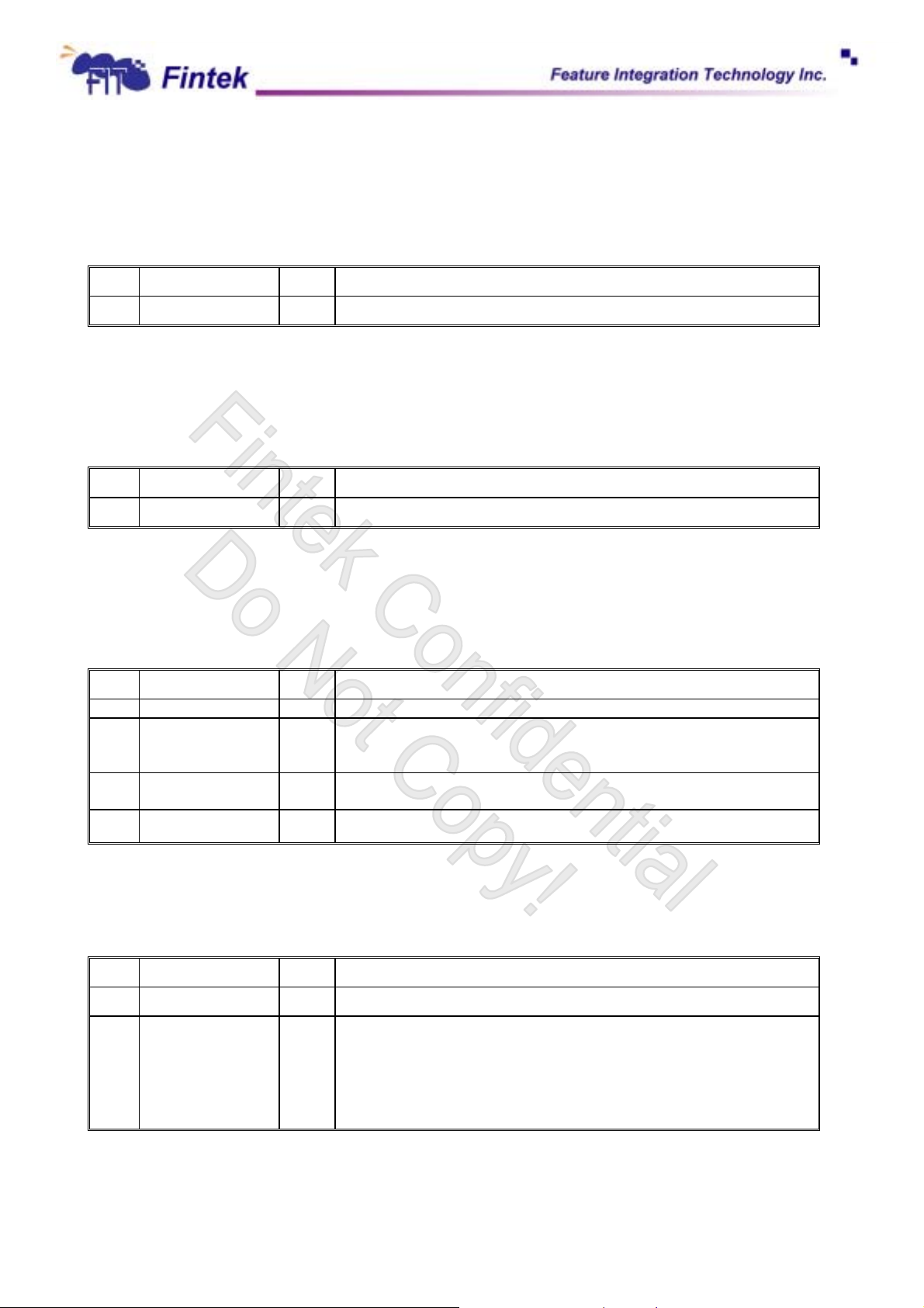
6.5.2 I/O Port Select Register – index 60h
Power-on default [7:0] = 0x02h when SOUT4/PS_2E8_IRQD is pull-up, else 0x00h.
Bit Name R/W Description
7:0 URD_BASE[15:8] R/W UART 4 I/O Port Address high byte.
6.5.3 I/O Port Select Register – index 61h
F81216D
Power-on default [7:0] = 0xE8h when SOUT4/PS_2E8_IRQD is pull-up, else 0x00h.
Bit Name R/W Description
7:0 URD_BASE[7:0] R/W UART 4 I/O Port Address low byte.
6.5.4 IRQ Channel Select Register – index 70h
Power-on default [7:0] = 0x09h when SOUT4/PS_2E8_IRQD is pull-up, else 0x00h.
Bit Name R/W Description
7:6 Reserved R/W Return 0 when read.
5 URDIRQ_MODE R/W 0 : PCI IRQ sharing mode
1 : ISA IRQ sharing mode.
This bit is effective in IRQ sharing mode.
4 URDIRQ_SHAR R/W 0 : IRQ is not sharing with other device.
1 : IRQ is sharing with other device.
3:0 SELURDIRQ[3:0] R/W Select the Serial IRQ channel.
6.5.6 UART 4 Clock Select Register – index F0h
Power-on default [7:0] = 0x00h.
Bit Name R/W Description
7:2 Reserved R/W Return 0 when read.
1:0 SELURDCLK1
SELURDCLK0
R/W 00b : UART 4 clock source is 1.8462MHz ( 24MHz/13 )
01b : UART 4 clock source is 18.462MHz ( 24MHz/1.3 )
10b : UART 4 clock source is 24MHz ( 24MHz/1 )
11b : UART 4 clock source is 14.769MHz ( 24MHz/1.625 )
-26-
July, 2004
V0.26P
Page 31
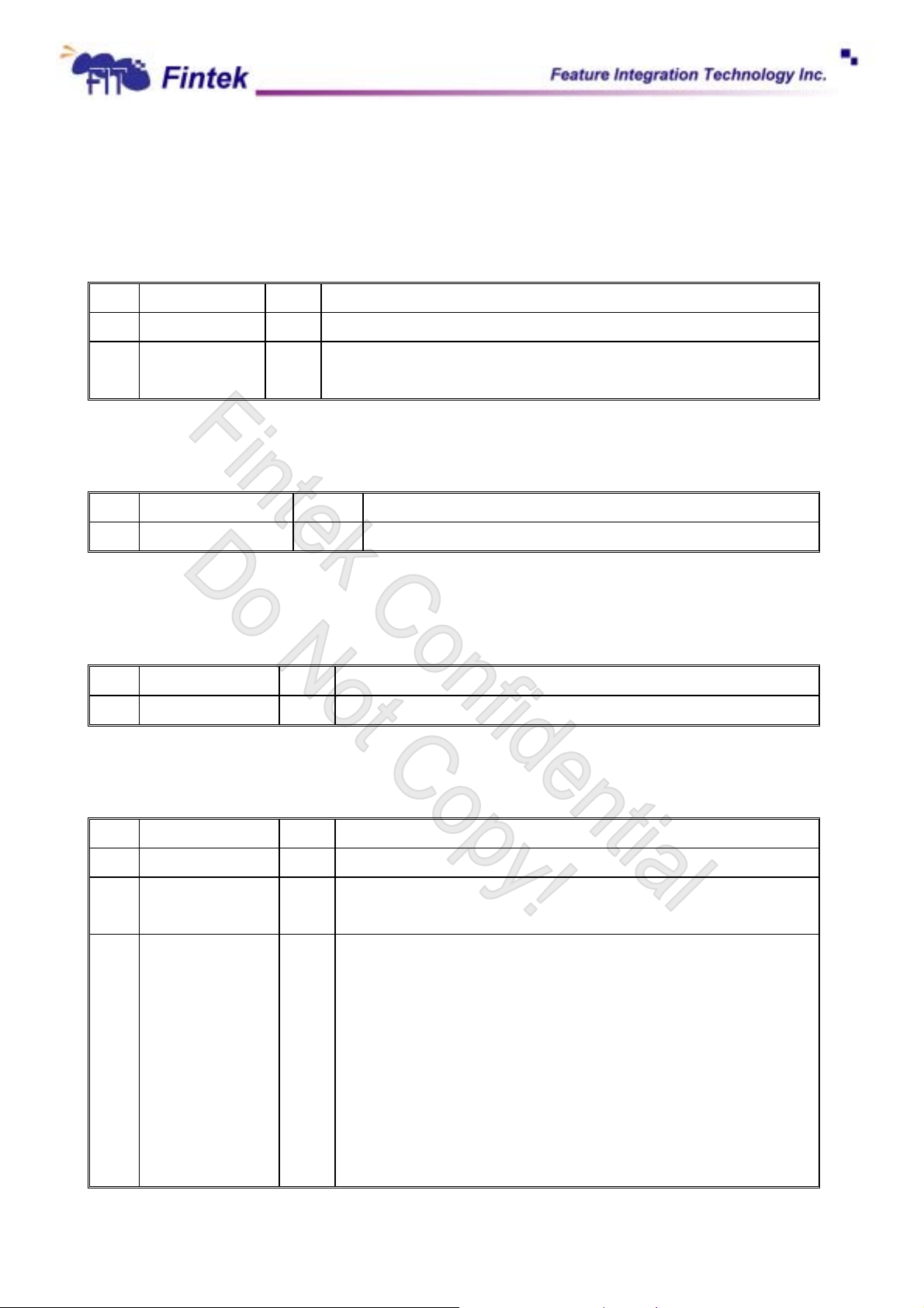
6.6 Watch Dog Timer Device Control Register (LDN 8)
6.6.1 Device Enable Register – index 30h
Power-on default [7:0] = 0x01h when DTR3#/PS_WDT is pull-up, else 0x00 h.
Bit Name R/W Description
7:1 Reserved R/W Return 0 when read.
F81216D
0 WDT_EN R/W 0 : Disable Watchdog Time r.
1 : Enable Watchdog Timer.
6.6.2 I/O Port Select Register – index 60h
Power-on default [7:0] = 0x04h when DTR3#/PS_WDT is pull-up, else 0x00 h.
Bit Name R/W Description
7:0 WDT_BASE[15:8] R/W I/O Base high byte.
6.6.3 I/O Port Select Register – index 61h
Power-on default [7:0] = 0x42h when DTR3#/PS_WDT is pull-up, else 0x00 h.
Bit Name R/W Description
7:0 WDT_BASE[7:0] R/W I/O Base low byte.
6.6.4 IRQ Channel Select Register – index 70h
Power-on default [7:0] = 0x00h.
Bit Name R/W Description
7:5 Reserved R/W Return 0 when read.
4 WDTIRQ_EN R/W 0 : Time out is asserted only via WDT_OUT#.
1 : Time out is asserted via IRQ and WDT_OUT#.
3:0 SELWDTIRQ[3:0] R/W In LPC mode , select the Serial IRQ channel.
In ISA mode , select one of six IRQ pins .
03h : use serial IRQ channel 3 in LPC mode or use ISA_IRQA in ISA
mode.
04h : use serial IRQ channel 4 in LPC mode or use ISA_IRQB in ISA
mode.
05h : use serial IRQ channel 5 in LPC mode or use IS A_IRQC in ISA
mode.
09h : use serial IRQ channel 9 in LPC mode or use IS A_IRQD in ISA
-27-
July, 2004
V0.26P
Page 32
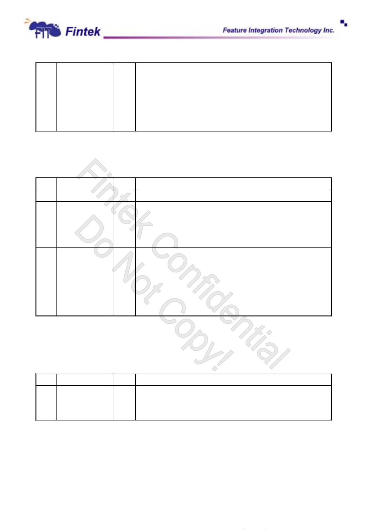
mode.
0Ah : use serial IRQ channel 10 in LPC mode or use ISA_IRQE in
ISA mode.
0Bh : use serial IRQ channel 11 in LPC mode or use ISA_IRQF in
ISA mode.
Otherwise will disable the interrupt.
6.6.5 Timer Status and Control Register – index F0h
Power-on default [7:0] = 0x02h when DTR3#/PS_WDT is pull-up , else 0x00h.
F81216D
Bit Name R/W Description
7:3 Reserved R/W Return 0 when read.
2:1 WDT_UNIT[1:0] R/W 00 : Timer Unit is 10ms.
0 WDT_EVENT R/W When read
01 : Timer Unit is 1 second
10 : Timer Unit is 1 minute.
11 : reserved.
0 : no time out occur.
1 : time out has occurred.
when write
0 : no action
1 : clear the time out status.
6.6.6 Timer Count Number Register – index F1h
Power-on default [7:0] = 0x0Ah when DTR3#/PS_WDT is pull-up, else 0x00h.
Bit Name R/W Description
7:0 WDT_CNT[7:0] R/W The number of count for watchdog timer.
Write the same value twice to enable the timer , otherwi se will disable
timer.
-28-
July, 2004
V0.26P
Page 33
F81216D
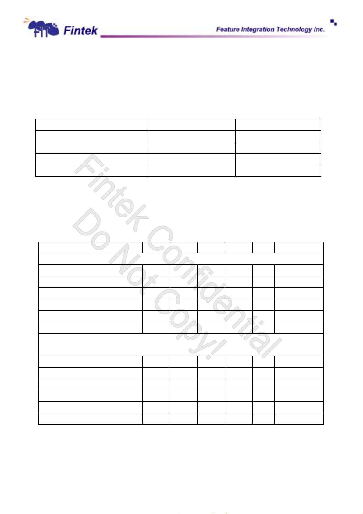
7. Electron Characteristic
7.1 Absolute Maximum Ratings
PARAMETER RATING UNIT
Power Supply V oltage -0.5 to 4.0 V
Input Volt age -0.5 to 5.5 V
Operating Temperature 0 to +70
° C
Storage Temperature -55 to +150
° C
Note: Exposure to conditions beyond those listed under Absolute Maximum Ratings may adversely affect the
life and reliability of the device.
7.2 DC Characteristics
((Ta = 0° C to 70° C, VDD = 3.3V ± 10%, VSS = 0V)
PARAMETER SYM. MIN. TYP. MAX. UNIT CONDITIONS
I/O
- TTL level bi-directional pin with source-sink capability of 12 mA
12t
Input Low Voltage VIL 0.8 V
Input High Voltage VIH 2.0 V
Output Low Current IOL 10 12 mA VOL = 0.4V
Output High Current IOH -12 -10 mA VOH = 2.4V
Input High Leakage ILIH +10
Input Low Leakage ILIL -10
I/O
- TTL level bi-directional pin with source-sink capability of 12 mA and schmitt-trigger level
12ts
input
Input Low Threshold Voltage Vt- 0.5 0.8 1.1 V VDD = 3.3 V
Input High Threshold Voltage Vt+ 1.6 2.0 2.4 V VDD = 3.3 V
µA
µA
VIN = VDD
VIN = 0V
Output Low Current IOL 10 12 mA VOL = 0.4 V
Output High Current IOH -12 -10 mA VOH = 2.4V
Input High Leakage ILIH +10
Input Low Leakage ILIL -10
-29-
µA
µA
VIN = VDD
VIN = 0V
July, 2004
V0.26P
Page 34
F81216D
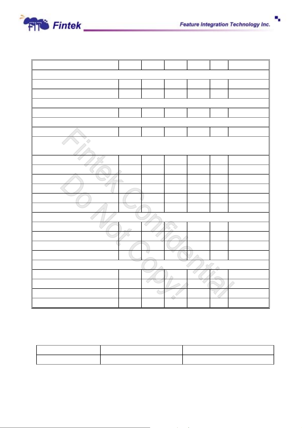
7.2 DC Characteristics, continued
PARAMETER SYM. MIN. TYP. MAX. UNIT CONDITIONS
OUT
Output Low Current IOL 12 16 mA VOL = 0.4V
Output High Current IOH -14 -12 mA VOH = 2.4V
OD8 - Open-drain output pin with sink capability of 8 mA
Output Low Current IOL 6 8 mA VOL = 0.4V
OD16 - Open-drain output pin with sink capability of 16 mA
Output Low Current IOL 12 16 mA VOL = 0.4V
I/OOD
Input Low Threshold Voltage Vt- 0.5 0.8 1.1 V VDD = 3.3 V
Input High Threshold Voltage Vt+ 1.6 2.0 2.4 V VDD = 3.3 V
Output Low Current IOL 6 8 mA VOL = 0.4 V
Output High Current IOH -16 -12 mA VOH = 2.4V
Input High Leakage ILIH +10
Input Low Leakage ILIL -10
INt - TTL level input pin
- TTL level output pin with source-sink capability of 12 mA
12t
- TTL level bi-directional pin, can select to OD or OUT by register, with 16 mA
16ts
source-sink capability
µA
µA
VIN = VDD
VIN = 0V
Input Low Voltage VIL 0.8 V
Input High Voltage VIH 2.0 V
Input High Leakage ILIH +10
Input Low Leakage ILIL -10
INts - TTL level Schmitt-triggered input pin
Input Low Threshold Voltage Vt- 0.5 0.8 1.1 V VDD = 3.3V
Input High Threshold Voltage Vt+ 1.6 2.0 2.4 V VDD = 3.3V
Input High Leakage ILIH +10
Input Low Leakage ILIL -10
µA
µA
µA
µA
VIN = VDD
VIN = 0 V
VIN = VDD
VIN = 0 V
8. Ordering Information
Part Number Package Type Production Flow
F81216D 48 - LQFP
Commercial, 0°C to +70°C
-30-
July, 2004
V0.26P
Page 35
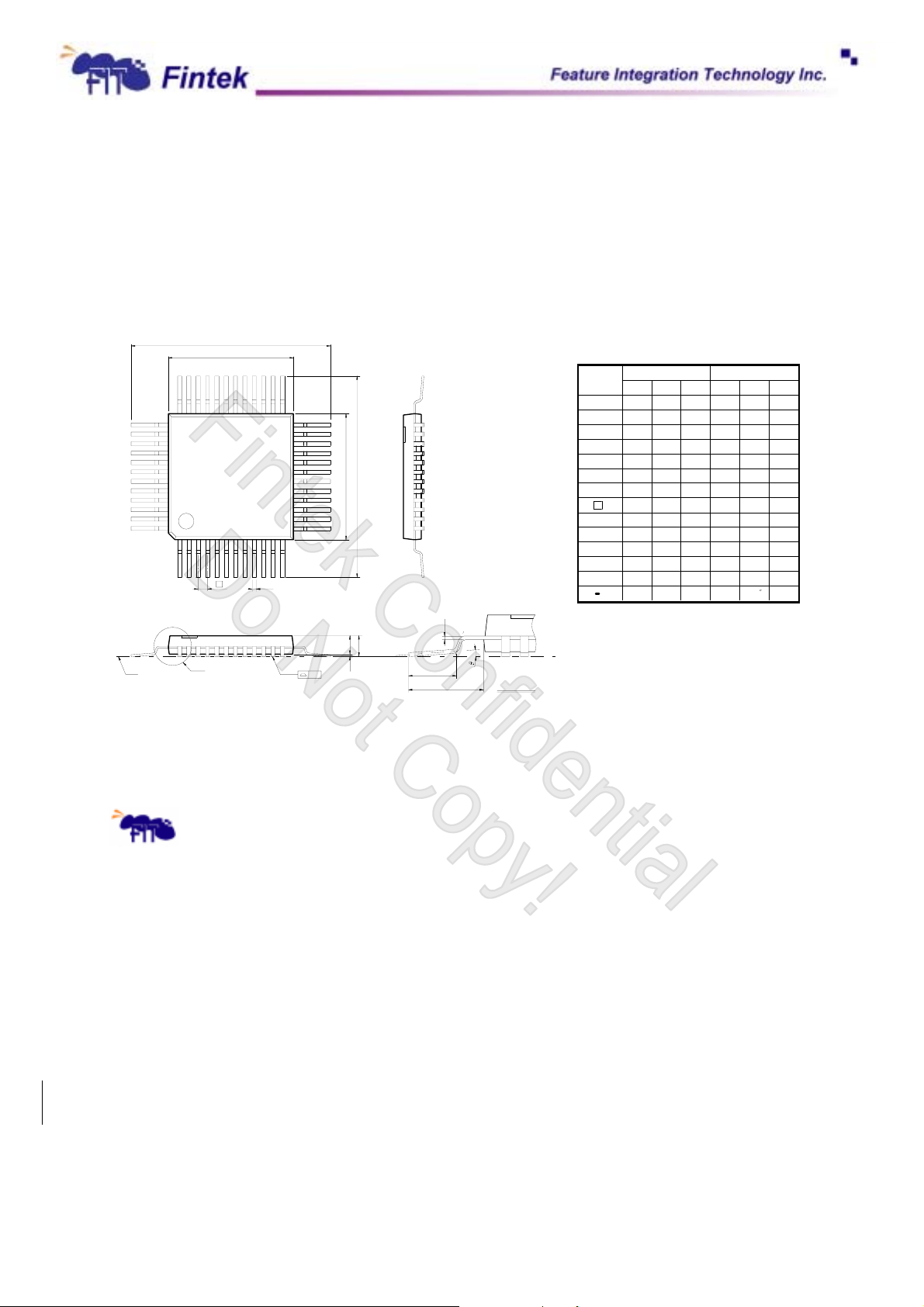
9. Package Dimensions
48pin-LQFP
D
H
D
36
37
25
24
E
E
H
48
Seating Plane
1
e
See Detail F
12
b
13
c
A
2
A
1
A
y
L
L
1
Detail F
F81216D
Dimension in inch Dimension in mm
Symbol
A
1
A
2
A
b
c
D
E
e
D
H
H
E
L
1
L
y
0
Notes:
1. Dimensions D & E do not include interlead
flash.
2. Dimension b does not include dambar
protrusion/intrusion.
3. Controlling dimension: Millimeters
4. General appearance spec. should be based
on final visual inspection spec.
Min.
Nom.
Max. Max.
Min.
---
0.05
1.35
0.17 0.27
0.09
0.45
--0
Nom.
---
---
1.40
0.20
---
7.00
7.00
0.50
9.00
9.00
0.60
1.00
0.08
3.5
1.60
0.15
1.45
0.20
0.75
--7
Feature Integration Technology Inc.
Headquaters
7F, No 31, Shintai Rd.,
Jubei City, Hsinchu 302, Taiwan, R.O.C.
TEL : 886-3-6562727
FAX : 886-3-6560537
www: http://www.fintek.com.tw
Please note that all datasheet and specifications are subject to change without notice. All the trade
marks of products and companies mentioned in this datasheet belong to their respective owne
r.
-31-
July, 2004
V0.26P
Page 36
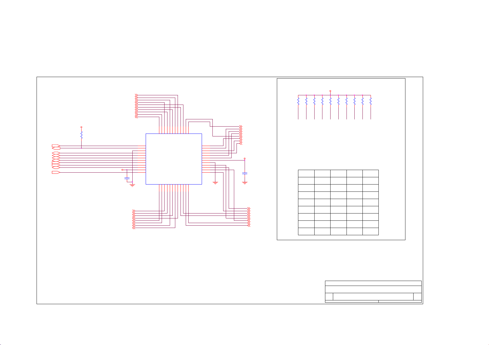
10. Application Circuit
PCIRST#
WDT_OUT#
LAD3
LAD2
LAD1
LAD0
PCICLK
LFRAME#
SERIRQ
CLK24IN
VCC3V
R1
4.7K
PIN_1
PIN_2
PIN_4
PIN_5
PIN_6
PIN_7
PIN_8
PIN_9
PIN_10
PIN_12
VCC3V
C2
0.1U
DCD1#
PIN_11
RTS4#
DTR4#
SOUT4
CTS4#
DSR4#
SIN4
DCD4#
RTS1#
DTR1#
SOUT1
RI1#
CTS1#
DSR1#
SIN1
IRRX
IRTX
RI4#
PIN_3
1
2
3
4
5
6
7
8
9
10
11
12
PCIRST#
WDT_OUT#
GND
LAD3
LAD2
LAD1
LAD0
LCLK
LFRAM#
SERIRQ
VCC
CLKIN
PIN_46
PIN_43
PIN_45
PIN_47
PIN_44
PIN_48
48
U1
RI1#
IRTX
IRRX
SOUT1
DCD1#
F81216D
CTS4#
DSR4#
RTS4#
DTR4#
SIN4
1314151617181920212223
PIN_17
PIN_18
PIN_16
PIN_14
PIN_15
PIN_13
(Power On Setting Pin)
R2
R4
R3
4.7K
4.7K
4.7K
PIN_18
PIN_38
PIN_42
SIN1
DTR1#
SOUT4
DCD4#
PIN_19
PIN_37
PIN_41
PIN_40
3738394041424344454647
RI2#
CTS1#
RTS1#
DSR1#
DCD2#
SOUT2
SIN2
DTR2#
RTS2#
DSR2#
CTS2#
VCC
GND
RI3#
DCD3#
SOUT3
SIN3
RI4#
CTS3#
DSR3#
RTS3#
DTR3#
24
PIN_21
PIN_23
PIN_24
PIN_20
PIN_22 PIN_39
PIN_36
36
PIN_35
35
PIN_34
34
PIN_33
33
PIN_32
32
PIN_31
31
PIN_30
30
PIN_29
29
PIN_28
28
PIN_27
27
PIN_26
26
PIN_25
25
DCD2#
SIN2
DSR2#
CTS2#
RI2#
SOUT2
DTR2#
RTS2#
VCC3V
C1
0.1U
DCD3#
SIN3
DSR3#
CTS3#
RI3#
SOUT3
DTR3#
RTS3#
PIN_23
R2 on: UART 4 addr:0x2e8 IRQ9; off:UART 4 disa bled.
R5 on: UART 3 addr:0x3e8 IRQ5; off:UART 3 disa bled.
R8 on : UART 2 addr:0x2f8 ir q4; R7 on and R8 off: UART 2 addr:0x2e0 IRQ4; R7
off and R8 off:UART 2 disabled.
R11 on : UART 1 addr:0x3f8 irq3; R10 on and R11 off: UAR T 1 ad dr:0x3e0 IRQ3;
R10 off and R11 off:UART 1 disabled.
R4 on: Watch Dog Timer enabled and setting to 10 se co nd when the clock input
is 24Mhz. If the clock input is 48Mhz , the timer is set ting to 5 second.
off :disabled.
R6
0
0
0
0
1
1
1
1
VCC3V
R6
R7
R8
R9
R10
R5
4.7K
4.7K
4.7K
PIN_24
PIN_26
R3
0
0
1
1
0
0
1
1
4.7K
PIN_34
PIN_33
R9
0
1
0
1
0
1
0
1 0x2e/0x2f
PIN_36
4.7K
PIN_41
Address
0x4e/0x4f
0x2e/0x2f
0x4e/0x4f
0x2e/0x2f
0x4e/0x4f
0x2e/0x2f
0x4e/0x4f
4.7K
R11
4.7K
PIN_42
Entry Key
0x77
0x77
0xa0
0xa0
0x87
0x87
0x67
0x67
PIN_44
On:1
Off:0
Title
Feature I nt e grat ion Tec hnolog y Inc .
Size Document Number Rev
F81216D 0.2
B
Date: Sheet
of
12Tuesday , Sep t em ber 16, 2003
Page 37
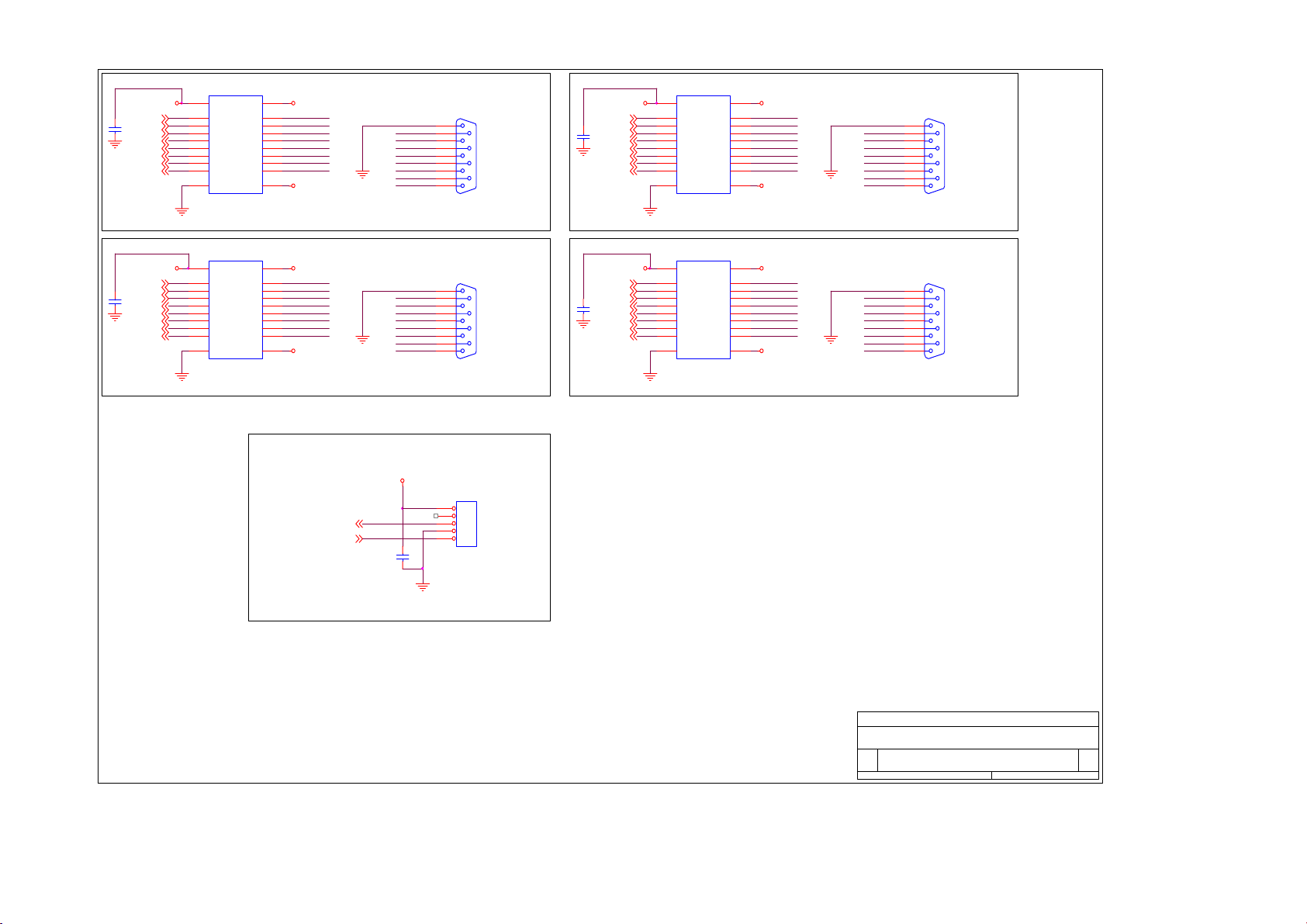
C3
0.1U
C5
0.1U
VCC5V
RTS1#
DTR1#
SOUT1
RI1#
CTS1#
DSR1#
SIN1
DCD1#
VCC5V
RTS2#
DTR2#
SOUT2
RI2#
CTS2#
DSR2#
SIN2
DCD2#
20
16
15
13
19
18
17
14
12
11
20
16
15
13
19
18
17
14
12
11
U2
VCC
DA1
DA2
DA3
RY1
RY2
RY3
RY4
RY5
GND
RS232
(SOP20)
U4
VCC
DA1
DA2
DA3
RY1
RY2
RY3
RY4
RY5
GND
RS232
(SOP20)
+12V
DY1
DY2
DY3
RA1
RA2
RA3
RA4
RA9
-12V
+12V
DY1
DY2
DY3
RA1
RA2
RA3
RA4
RA9
-12V
1
5
6
8
2
3
4
7
9
10
1
5
6
8
2
3
4
7
9
10
+12V
RTS1
DTR1
SOUT1RI1
CTS1
DSR1
SIN1DCD1
-12V
(UART1)
+12V
RTS2
DTR2
SOUT2RI2
CTS2
DSR2
SIN2DCD2
-12V
(UART2)
IRRX
IRTX
C7
0.1U
RI1
DTR1
CTS1
SOUT1RTS1
SIN1DSR1
DCD1
RI2
DTR2
CTS2
SOUT2RTS2
SIN2DSR2
DCD2
VCC3V
DB9
DB9
5
9
4
8
3
7
2
6
1
5
9
4
8
3
7
2
6
1
P1
P3
JP1
1
2
3
4
5
HEADER 5
C4
0.1U
C6
0.1U
RTS3#
DTR3#
SOUT3
RI3#
CTS3#
DSR3#
SIN3
DCD3#
RTS4#
DTR4#
SOUT4
RI4#
CTS4#
DSR4#
SIN4
DCD4#
VCC5V
VCC5V
20
16
15
13
19
18
17
14
12
11
20
16
15
13
19
18
17
14
12
11
U3
VCC
DA1
DA2
DA3
RY1
RY2
RY3
RY4
RY5
GND
RS232
(SOP20)
U5
VCC
DA1
DA2
DA3
RY1
RY2
RY3
RY4
RY5
GND
RS232
(SOP20)
+12V
DY1
DY2
DY3
RA1
RA2
RA3
RA4
RA9
-12V
+12V
DY1
DY2
DY3
RA1
RA2
RA3
RA4
RA9
-12V
1
+12V
5
RTS3
6
DTR3
SOUT3-
8
RI3
2
CTS3
3
DSR3
4
SIN3-
7
DCD3
9
10
-12V
RI3
DTR3
CTS3
SOUT3RTS3
SIN3DSR3
DCD3
(UART3)
1
+12V
RTS4
5
DTR4
6
8
SOUT4RI4
2
CTS4
3
DSR4
4
7
SIN4DCD4
9
10
-12V
RI4
DTR4
CTS4
SOUT4RTS4
SIN4DSR4
DCD4
(UART4)
DB9
DB9
P2
5
9
4
8
3
7
2
6
1
P4
5
9
4
8
3
7
2
6
1
(IrDA)
Title
Feature I nt egrat ion Technology Inc .
Size Document N um ber Rev
UART 0.2
B
Date: Sheet
22Tuesday, September 16, 2003
of
 Loading...