

Page 1

F71868A
Super I/O + Hardware Monitor
Release Date: May, 2015
Revision: V0.17P
Page 2
F71868A
Version
Date
Page
Revision History
0.10P
2011/02
Preliminary version
0.11P
2011/05
105
141, 145
14
70
85
1. Make Correction and Clarification
2. Modify Auto Swap Register Index FEh, bit 7
3. Update Application Circuits
4. Update FANCTL1~3 Pin Description
5. Update Voltage reading and limit Index 29h
6. Update Fan3 Control Register Index 9Ah bit0
0.12P
2011/06
53
140
1. Make Correction and Clarification
2. Update Multi-Function Select Register 1 Index 28 bit7 description
3. Update Package Dimension
0.13P
2011/12
1. Made Clarification & Modification
2. Multi-Function Select Register 5—Index 2Ch, bit [4:1]
3. GPIO0 Output Enable Register—Index F0h, bit 0
4. GPIO0 Output Data Register— Index F1h, bit 0
5. GPIO Pin Status Register — Index F2h
6. GPIO Drive Enable Register— Index F3h, bit 0
7. ERP S5 Delay Register— Index E7h
8. Update Index no. (GPIO7 Output Data Register Index 81h)
9. Update Index no.(GPIO7 Pin Status Register Index 82h)
10. Update Index no. (GPIO7 Drive Enable Register Index 83h)
11. Update Index no. (User Wakeup Code Register Index FFh)
12. SMB Protocol Select – Index EFh, bit 3-0
13. Update Application Circuit (Add Divided Resister Accuracy 1% at Voltage)
0.14P
2012/07
14
49
51
51
61
77
130
130
130
130
133
134
137
141
148
This datasheet is prepared for new version F71868A IC.
1. Update Pin 126~128 GPIO as Default function.
2. Add Chapter 5.7.2 PWROK sequence
3. Add Chapter 5.8 PSIN# Detecting Flag
4. Add 5.9 AC Loss & Resume Control Methods
5. Remove OVP power on strapped function and change default value:
Configuration Port Select Register Index 27h
6. Reserved Voltage Protection Power Good Select Register Index 3Fh
7. Reserved this bit is decided by RTS1# power-on trapping (WDOUT_EN
Index F0h[7]).
8. Reserved WDOUT_EN Index F0h[0].
9. Reserved Serial Key Data Register 1 Index F2h and Serial Key Data
Register 2 Index F3h.
10. Reserved this bit is decided by RTS1# power-on trapping (Watchdog
Timer Configuration Register 1 Index F5h (Offset 05h)[5]).
11. Add ERP Deep S5 Delay Register Index E7h
12. Add ERP Deep S3 Delay Register Index E9h
13. Add Keep Last State Select Register Index F4h [6]
14. Add PWROK Gate Enable Register and PSIN# Detect Register Index
FBh
15. Update Application Circuit sheet 1
0.15P
2012/10
21
23
60
132
1. Update pin description of FANCTL1 and FANCTL2.
2. Remove 4.7 GPIO53/54 PWM Control
3. Update 6.1.3 Chip ID
4. Update Output pulse width of RSTOUT# of WD_PSWIDTH within
F71868A Datasheet Revision History
May, 2015
V0.17P
Page 3
F71868A
150
153
Watchdog Timer Configuration Register 1 Index F5h [1:0].
5. Update 13. Application Circuit UART connecting resistance.
6. Update 13. Application Circuit PWM 4 Pin Fan Circuit for abnormal over
voltage protection circuit.
0.16P
2013/12
-
Made correction and modification
In section 4.1, update I_VSB3V and VBAT power pin description
In section 4.3, correct output current ability of GPIO20-27
In section 4.7, reserved push pull mode of GPIO50/51/52/53/54
In section 4.8, reserved push pull mode of GPIO47
In section 4.9, correct output current ability of GPIO13
Add section 5.10 General-Pulpose Input/Output (GPIO) Ports
In section 6.7.26, reserved B3h[7] push pull mode
In section 6.8.8, update Watchdog Timer Configuration Register 1 – Index
F5h [1:0]
In section 12, updated UART RI# application circuit
0.17P
2015/05
-
Made corrdction and modification
In section 9, update Top Marking Specification
Please note that all data and specifications are subject to change without notice. All the trade marks of products and companies
mentioned in this data sheet belong to their respective owners.
LIFE SUPPORT APPLICAT
These products are not designed for use in life support appliances, devices, or systems where malfunction of these products can
reasonably be expected to result in personal injury. Customers using or selling these products for use in such applications do so
at their own risk and agree to fully indemnify Fintek for any damages resulting from such improper use or sales.
May, 2015
V0.17P
Page 4

F71868A
Table of Content
1. General Description ........................................................................................................................................... 12
2. Feature List ........................................................................................................................................................ 13
3. Pin Configuration ............................................................................................................................................... 15
4. Pin Description .................................................................................................................................................. 16
4.1 Power Pins ........................................................................................................................................... 16
4.2 LPC Interface ....................................................................................................................................... 16
4.3 UART and SIR...................................................................................................................................... 16
4.4 Parallel Port .......................................................................................................................................... 18
4.5 Hardware Monitor ................................................................................................................................. 19
4.6 KBC Function ....................................................................................................................................... 21
4.7 GPIO 21
4.8 ACPI Function Pins .............................................................................................................................. 22
4.9 Power Saving and Others .................................................................................................................... 23
5. Function Description .......................................................................................................................................... 25
5.1 Power on Strapping Option .................................................................................................................. 25
5.2 Hardware Monitor ................................................................................................................................. 25
5.2.1. Table Range: ........................................................................................................................................ 26
5.2.2. Monitor Temperature from “Thermistor” ............................................................................................... 27
5.2.3. Monitor Temperature from “Thermal diode” ......................................................................................... 27
5.2.4. ADC Noise Filtering.............................................................................................................................. 27
5.2.5. Monitor Temperature from “SMBus device” ......................................................................................... 27
5.2.6. Monitor Temperature from “PECI” ........................................................................................................ 27
5.2.7. Temperature OVT# Signal ................................................................................................................... 28
5.2.8. Temperature PME# .............................................................................................................................. 28
5.2.9. Fan Speed Count ................................................................................................................................. 29
5.2.10. Fan Speed Control ............................................................................................................................... 29
5.2.11. Fan Speed Control Mechanism ............................................................................................................ 31
5.2.12. Fan Speed Control with Multi-temperature. ......................................................................................... 37
5.2.13. FAN_FAULT# ....................................................................................................................................... 39
5.2.14. Over Voltage Protection ....................................................................................................................... 40
5.3 ACPI Function ...................................................................................................................................... 41
5.4 AMD Power Timing Control Sequence ................................................................................................ 43
5.5 Intel PECI 3.0 Functions ...................................................................................................................... 44
5.6 S3_Gate#, S3P5_Gate# and S0P5_Gate# Timing .............................................................................. 45
May, 2015
V0.17P
Page 5

F71868A
5.7 Power Saving Function ........................................................................................................................ 46
5.7.2 PWROK sequence ......................................................................................................................... 49
5.7.3 Intel Cougar Point Timing (CPT) .................................................................................................... 50
5.8 PSIN# Detecting Flag ................................................................................................................................. 51
5.9 AC Loss & Resume Control Methods ......................................................................................................... 52
5.10 General-Pulpose Input/Output (GPIO) Ports ............................................................................................ 54
6. Register Description .......................................................................................................................................... 57
6.1 Global Control Registers ...................................................................................................................... 62
6.2 UART1 Registers (CR01)..................................................................................................................... 71
6.2.1 UART 1 Device Enable Register Index 30h ........................................................................ 71
6.2.2 Base Address High Register Index 60h ............................................................................... 71
6.2.3 Base Address Low Register Index 61h ................................................................................ 71
6.2.4 IRQ Channel Select Register Index 70h .............................................................................. 72
6.2.5 RS485 Enable Register Index F0h ...................................................................................... 72
6.3 UART2 Registers (CR02)..................................................................................................................... 72
6.3.1 UART 2 Device Enable Register Index 30h ........................................................................ 72
6.3.2 Base Address High Register Index 60h ............................................................................... 72
6.3.3 Base Address Low Register Index 61h ................................................................................ 72
6.3.4 IRQ Channel Select Register Index 70h .............................................................................. 72
6.3.5 RS485 Enable Register Index F0h ...................................................................................... 73
6.3.6 SIR Mode Control Register Index F1h ................................................................................. 73
6.4 Parallel Port Register (CR03) .............................................................................................................. 73
6.4.1 Parallel Port Device Enable Register Index 30h .................................................................. 73
6.4.2 Base Address High Register Index 60h ............................................................................... 74
6.4.3 Base Address Low Register Index 61h ................................................................................ 74
6.4.4 IRQ Channel Select Register Index 70h .............................................................................. 74
6.4.5 DMA Channel Select Register Index 74h ............................................................................ 74
6.4.6 PRT Mode Select Register Index F0h ................................................................................. 74
6.5 Hardware Monitor Registers (CR04) .................................................................................................... 75
6.5.1 Hardware Monitor Configuration Registers Index 30h......................................................... 75
6.5.2 Base Address High Register Index 60h ............................................................................... 75
6.5.3 Base Address Low Register Index 61h ................................................................................ 75
6.5.4 IRQ Channel Select Register Index 70h .............................................................................. 75
6.5.5 Configuration Register Index 01h ........................................................................................ 76
6.5.6 Configuration Register Index 02h ........................................................................................ 76
6.5.7 Configuration Register Index 03h ........................................................................................ 76
6.5.8 NEW TSI Mode Enable Register Index 07h .................................................................... 77
May, 2015
V0.17P
Page 6

F71868A
6.5.9 Configuration Register Index 08h ........................................................................................ 77
6.5.10 Configuration Register Index 09h ........................................................................................ 77
6.5.11 Configuration Register Index 0Ah ........................................................................................ 77
6.5.12 Configuration Register Index 0Bh ........................................................................................ 78
6.5.13 Configuration Register Index 0Ch ....................................................................................... 79
6.5.14 Configuration Register Index 0Dh ....................................................................................... 79
6.5.15 Configuration Register Index 0Fh ........................................................................................ 79
6.5.16 Voltage-Protect Shut Down Enable Register Index 10h ...................................................... 79
6.5.17 Voltage-Protect Status Register (Powered by VBAT) Index 11h ......................................... 79
6.5.18 Voltage-Protect Configuration Register (Powered by VBAT) Index 12h .............................. 80
6.5.19 Voltage Protection Power Good Select Register Index 3Fh ................................................ 80
6.5.20 Voltage reading and limit Index 20h- 37h ............................................................................. 80
6.5.21 PECI Configuration Register Index 40h ............................................................................... 81
6.5.22 PECI Master Control Register Index 41h ............................................................................ 82
6.5.23 PECI Master Status Register Index 42h .............................................................................. 82
6.5.24 PECI Master DATA0 Register Index 43h ............................................................................. 82
6.5.25 PECI Master DATA1 Register Index 44h ............................................................................. 82
6.5.26 PECI Master DATA2 Register Index 45h ............................................................................. 82
6.5.27 PECI Master DATA3 Register Index 46h ............................................................................. 83
6.5.28 PECI Master DATA4 Register Index 47h ............................................................................. 83
6.5.29 PECI Master DATA5 Register Index 48h ............................................................................. 83
6.5.30 PECI Master DATA6 Register Index 49h ............................................................................. 83
6.5.31 PECI Master DATA7 Register Index 4Ah ............................................................................. 83
6.5.32 PECI Master DATA8 Register Index 4Bh ............................................................................. 83
6.5.33 PECI Master DATA9 Register Index 4Ch ............................................................................ 84
6.5.34 PECI Master DATA10 Register Index 4Dh .......................................................................... 84
6.5.35 PECI Master DATA11 Register Index 4Eh ........................................................................... 84
6.5.36 PECI Master DATA12 Register Index 4Fh ........................................................................... 84
6.5.37 Temperature PME# Enable Register Index 60h .................................................................. 84
6.5.38 Temperature Interrupt Status Register Index 61h ................................................................ 84
6.5.39 Temperature Real Time Status Register Index 62h ............................................................. 85
6.5.40 Temperature BEEP Enable Register Index 63h .................................................................. 86
6.5.41 T1 OVT and High Limit Temperature Select Register Index 64h ........................................ 86
6.5.42 OVT and Alert Output Enable Register 1 Index 66h ............................................................ 87
6.5.43 Reserved Index 67~69h ....................................................................................................... 87
6.5.44 Temperature Sensor Type Register Index 6Bh .................................................................... 87
6.5.45 TEMP1 Limit Hystersis Select Register Index 6Ch ............................................................. 88
May, 2015
V0.17P
Page 7

F71868A
6.5.46 TEMP2 and TEMP3 Limit Hystersis Select Register Index 6Dh ......................................... 88
6.5.47 DIODE OPEN Status Register Index 6Fh ............................................................................ 88
6.5.48 Temperature Index 70h- 8Dh ............................................................................................... 88
6.5.49 Temperature Filter Select Register Index 8Eh ...................................................................... 89
6.5.50 FAN PME# Enable Register Index 90h ............................................................................... 90
6.5.51 FAN Interrupt Status Register Index 91h ............................................................................. 90
6.5.52 FAN Real Time Status Register Index 92h .......................................................................... 91
6.5.53 FAN BEEP# Enable Register Index 93h .............................................................................. 91
6.5.54 FAN Type Select Register Index 94h (FAN_PROG_SEL = 0) ............................................. 91
6.5.55 FAN Type Select Register Index 94h (FAN_PROG_SEL = 1) ............................................. 92
6.5.56 FAN1 Temperature Adjust Rate Register Index 95h (FAN_PROG_SEL = 1) ...................... 93
6.5.57 FAN mode Select Register Index 96h (FAN_PROG_SEL = 0) ........................................... 93
6.5.58 FAN mode Select Register Index 96h (FAN_PROG_SEL = 1) ........................................... 94
6.5.59 Auto FAN1 and FAN2 Boundary Hystersis Select Register Index 98h ............................... 95
6.5.60 Auto FAN3 Boundary Hystersis Select Register Index 99h ................................................. 95
6.5.61 Fan3 Control Register Index 9Ah ........................................................................................ 95
6.5.62 Auto Fan Up Speed Update Rate Select Register Index 9Bh (FAN_PROG_SEL = 0) ........ 96
6.5.1 Auto Fan Up Speed Update Rate Select Register Index 9Bh (FAN_PROG_SEL = 1) ........ 96
6.5.2 FAN1 and FAN2 START UP DUTY-CYCLE/VOLTAGE Index 9Ch ..................................... 97
6.5.3 FAN3 START UP DUTY-CYCLE/VOLTAGE Index 9Dh ....................................................... 97
6.5.4 FAN PROGRAMMABLE DUTY-CYCLE/VOLTAGE LOADED AFTER POWER-ON Index 9Eh
98
6.5.5 Fan Fault Time Register Index 9Fh ..................................................................................... 98
6.5.6 FAN1 Index A0h~AFh ............................................................................................................... 98
6.5.7 VT1 BOUNDARY 1 TEMPERATURE – Index A6h .................................................................. 99
6.5.8 VT1 BOUNDARY 2 TEMPERATURE – Index A7 .................................................................... 99
6.5.9 VT1 BOUNDARY 3 TEMPERATURE – Index A8h .................................................................. 99
6.5.10 VT1 BOUNDARY 4 TEMPERATURE – Index A9 .................................................................. 100
6.5.11 FAN1 SEGMENT 1 SPEED COUNT – Index AAh ................................................................. 100
6.5.12 FAN1 SEGMENT 2 SPEED COUNT – Index ABh ................................................................. 100
6.5.13 FAN1 SEGMENT 3 SPEED COUNT Register – Index ACh .................................................. 100
6.5.14 FAN1 SEGMENT 4 SPEED COUNT Register – Index ADh .................................................. 101
6.5.15 R/W ......................................................................................................................................... 101
6.5.74 FAN1 SEGMENT 5 SPEED COUNT Register – Index AEh ................................................... 101
6.5.16 FAN1 Temperature Mapping Select – Index AFh ................................................................... 101
6.5.17 FAN2 Index B0h~BFh ............................................................................................................. 102
6.5.18 VT2 BOUNDARY 1 TEMPERATURE – Index B6h ................................................................ 103
May, 2015
V0.17P
Page 8

F71868A
6.5.19 VT2 BOUNDARY 2 TEMPERATURE – Index B7 .................................................................. 103
6.5.20 VT2 BOUNDARY 3 TEMPERATURE – Index B8h ................................................................ 104
6.5.21 VT2 BOUNDARY 4 TEMPERATURE – Index B9 .................................................................. 104
6.5.22 FAN2 SEGMENT 1 SPEED COUNT – Index BAh ................................................................. 104
6.5.23 FAN2 SEGMENT 2 SPEED COUNT – Index BBh .............................................................. 104
6.5.24 FAN2 SEGMENT 3 SPEED COUNT Register – Index BCh .................................................. 105
6.5.25 FAN2 SEGMENT 4 SPEED COUNT Register – Index BDh .................................................. 105
6.5.26 FAN2 SEGMENT 5 SPEED COUNT Register – Index BEh .................................................. 105
6.5.27 FAN2 Temperature Mapping Select – Index BFh ................................................................... 105
6.5.28 FAN3 Index C0h- CFh ............................................................................................................ 106
6.5.29 VT3 BOUNDARY 1 TEMPERATURE – Index C6h ................................................................ 107
6.5.30 VT3 BOUNDARY 2 TEMPERATURE – Index C7 .................................................................. 107
6.5.31 VT3 BOUNDARY 3 TEMPERATURE – Index C8h ................................................................ 107
6.5.32 VT3 BOUNDARY 4 TEMPERATURE – Index C9 .................................................................. 108
6.5.33 FAN3 SEGMENT 1 SPEED COUNT – Index CAh ................................................................. 108
6.5.34 FAN3 SEGMENT 2 SPEED COUNT – Index CBh ................................................................. 108
6.5.35 FAN3 SEGMENT 3 SPEED COUNT – Index CCh ............................................................ 108
6.5.36 FAN3 SEGMENT 4 SPEED COUNT – Index CDh ............................................................ 109
6.5.37 FAN3 SEGMENT 5 SPEED COUNT – Index CEh ............................................................ 109
6.5.38 FAN3 Temperature Mapping Select – Index CFh ................................................................... 109
6.5.39 TSI Temperature 0 – Index E0h .............................................................................................. 110
6.5.40 TSI Temperature 1 – Index E1h .............................................................................................. 111
6.5.41 TSI Temperature 2 Low Byte – Index E2h............................................................................... 111
6.5.42 TSI Temperature 2 High Byte – Index E3h .............................................................................. 111
6.5.43 TSI Temperature 3 – Index E4h .............................................................................................. 112
6.5.44 TSI Temperature 4 – Index E5h .............................................................................................. 112
6.5.45 TSI Temperature 5 – Index E6h .............................................................................................. 112
6.5.46 TSI Temperature 6 – Index E7h .............................................................................................. 112
6.5.47 TSI Temperature 7 – Index E8h .............................................................................................. 113
6.5.48 SMB Data Buffer 9 – Index E9h .............................................................................................. 113
6.5.49 Block Write Count Register – Index ECh ................................................................................ 113
6.5.50 SMB Command Byte/TSI Command Byte – Index EDh ......................................................... 113
6.5.51 SMB Status – Index EEh ......................................................................................................... 114
6.5.52 SMB Protocol Select – Index EFh ........................................................................................... 114
6.6 KBC Registers (CR05) ........................................................................................................................ 116
6.7 GPIO Registers (CR06) ...................................................................................................................... 117
6.7.1 GPIO Device Enable Register Index 30h ........................................................................... 117
May, 2015
V0.17P
Page 9

F71868A
6.7.2 Base Address High Register Index 60h .............................................................................. 117
6.7.3 Base Address Low Register Index 61h ............................................................................... 117
6.7.4 GPIRQ Channel Select Register Index 70h ....................................................................... 117
6.7.5 GPIO0 Output Enable Register Index F0h ......................................................................... 117
6.7.6 GPIO0 Output Data Register Index F1h ............................................................................. 118
6.7.7 GPIO Pin Status Register Index F2h .................................................................................. 118
6.7.8 GPIO Drive Enable Register Index F3h .............................................................................. 118
6.7.9 GPIO1 Output Enable Register Index E0h ......................................................................... 119
6.7.10 GPIO1 Output Data Register Index E1h ............................................................................. 119
6.7.11 GPIO1 Pin Status Register Index E2h ............................................................................... 120
6.7.12 GPIO1 Drive Enable Register Index E3h .......................................................................... 120
6.7.13 GPIO1 PME Enable Register Index E4h ........................................................................... 120
6.7.14 GPIO1 Input Detection Select Register Index E5h ............................................................ 121
6.7.15 GPIO1 Event Status Register Index E6h ........................................................................... 121
6.7.16 GPIO2 Output Enable Register Index D0h ........................................................................ 122
6.7.17 GPIO2 Output Data Register Index D1h ........................................................................... 122
6.7.18 GPIO2 Pin Status Register Index D2h ............................................................................... 123
6.7.19 GPIO2 Drive Enable Register Index D3h .......................................................................... 123
6.7.20 GPIO3 Output Enable Register Index C0h ........................................................................ 123
6.7.21 GPIO3 Output Data Register Index C1h ........................................................................... 124
6.7.22 GPIO3 Pin Status Register Index C2h ............................................................................... 124
6.7.23 GPIO4 Output Enable Register Index B0h ........................................................................ 125
6.7.24 GPIO4 Output Data Register Index B1h ............................................................................ 125
6.7.25 GPIO4 Pin Status Register Index B2h ............................................................................... 125
6.7.26 GPIO4 Drive Enable Register Index B3h .......................................................................... 126
6.7.27 GPIO4 PME Enable Register Index B4h ........................................................................... 126
6.7.28 GPIO4 Input Detection Select Register Index B5h ............................................................ 126
6.7.29 GPIO4 Event Status Register Index B6h ........................................................................... 127
6.7.30 GPIO5 Output Enable Register Index A0h ........................................................................ 127
6.7.31 GPIO5 Output Data Register Index A1h ............................................................................ 128
6.7.32 GPIO5 Pin Status Register Index A2h ............................................................................... 128
6.7.33 GPIO5 PME Enable Register Index A4h ........................................................................... 128
6.7.34 GPIO5 Input Detection Select Register Index A5h ............................................................ 128
6.7.35 GPIO5 Event Status Register Index A6h ........................................................................... 129
6.7.36 GPIO6 Output Enable Register Index 90h ........................................................................ 130
6.7.37 GPIO6 Output Data Register Index 91h ............................................................................ 130
6.7.38 GPIO6 Pin Status Register Index 92h ............................................................................... 131
May, 2015
V0.17P
Page 10

F71868A
6.7.39 GPIO6 Drive Enable Register Index 93h ........................................................................... 131
6.7.40 GPIO7 Output Enable Register Index 80h ........................................................................ 131
6.7.41 GPIO7 Output Data Register Index 81h ............................................................................ 132
6.7.42 GPIO7 Pin Status Register Index 82h ............................................................................... 132
6.7.43 GPIO7 Drive Enable Register Index 83h ........................................................................... 132
6.8 Watch Dog Timer Registers (CR07) .................................................................................................. 133
6.8.1 WDT Enable Register Index 30h ....................................................................................... 133
6.8.2 Base Address High Register Index 60h ............................................................................. 133
6.8.3 Base Address Low Register Index 61h .............................................................................. 133
6.8.4 WDOUT_EN Index F0h (Offset 00h) ................................................................................. 133
6.8.5 Serial Key Data Register 1 Index F2h (Offset 02h) ........................................................... 134
6.8.6 Serial Key Data Register 2 Index F3h (Offset 03h) ........................................................... 134
6.8.7 Reserved Index F4h (Offset 04h) ...................................................................................... 134
6.8.8 Watchdog Timer Configuration Register 1 Index F5h (Offset 05h) ..................................... 134
6.8.9 Watchdog Timer Configuration Register 2 Index F6h (Offset 06h) .................................... 134
6.8.10 WDT PME Register Index F7h (Offset 07h) ...................................................................... 134
6.9 PME, ACPI, and ERP Power Saving Registers (CR0A) .................................................................... 135
6.9.1 Device Enable Register Index 30h .................................................................................... 135
6.9.2 ERP Enable Register Index E0h ........................................................................................ 135
6.9.3 ERP control register Index E1h ......................................................................................... 136
6.9.4 ERP control register Index E2h ......................................................................................... 136
6.9.5 ERP PSIN deb-register Index E3h ..................................................................................... 136
6.9.6 ERP RSMRST deb-register Index E4h .............................................................................. 136
6.9.7 ERP PSOUT deb-register Index E5h ................................................................................. 136
6.9.8 ERP PSON deb-register Index E6h ................................................................................... 137
6.9.9 ERP Deep S5 Delay Register Index E7h .......................................................................... 137
6.9.10 Wakeup Enable register Index E8h ................................................................................... 137
6.9.11 ERP Deep S3 Delay Register Index E9h .......................................................................... 137
6.9.12 ERP Mode Select register Index ECh................................................................................ 137
6.9.13 ERP WDT Control register Index EDh ............................................................................... 137
6.9.14 ERP WDT Timer Index EEh ............................................................................................... 138
6.9.15 PME Event Enable Register 1 Index F0h ........................................................................... 138
6.9.16 PME Event Status Register Index F1h .............................................................................. 138
6.9.17 PME Event Enable Register 2 Index F2h .......................................................................... 139
6.9.18 PME Event Status Register Index F3h .............................................................................. 139
6.9.19 Keep Last State Select Register Index F4h ....................................................................... 140
6.9.20 VDDOK Delay Register Index F5h (powered by VBAT) .................................................... 140
May, 2015
V0.17P
Page 11

F71868A
6.9.21 PCIRST Control Register Index F6h.................................................................................. 141
6.9.22 Power Sequence Control Register Index F7h (powered by VBAT) ................................... 141
6.9.23 LED VCC Mode Select Register Index F8h ....................................................................... 142
6.9.24 LED VSB Mode Select Register Index F9h ....................................................................... 142
6.9.25 LED Additional Mode Select Register Index FAh .............................................................. 143
5.9.26 PWROK Gate Enable Register and PSIN# Detect Register Index FBh ............................ 145
5.9.27 Intel DSW Delay Select Register Index FCh ..................................................................... 146
5.9.28 RI De-bounce Select Register Index FEh .......................................................................... 146
7. Electrical Characteristics ................................................................................................................................. 147
7.1 Absolute Maximum Ratings ............................................................................................................... 147
7.2 DC Characteristics ............................................................................................................................. 147
8. Ordering Information ....................................................................................................................................... 151
9. Top Marking Specification ................................................................................................................................ 151
10. Package Dimensions (128-LQFP) .................................................................................................................. 152
10. Application Circuit ............................................................................................................................................ 153
May, 2015
V0.17P
Page 12

12
F71868A
1. General Description
The F71868A which is the featured IO chip for PC system is equipped with one IEEE 1284
Parallel Port, two UART Ports, one 80 port (multi with COM2), Hardware Keyboard Controller,
and SIR. The F71868A integrates with hardware monitor, 9 sets of voltage sensor, 3 sets of
creative auto-controlling fans and 3 temperature sensor pins for the accurate dual current type
temperature measurement for CPU thermal diode or external transistors 2N3906. Others, the
F71868A supports newest AMD TSI and Intel PECI 3.0 interfaces and INTEL Ibex PEAK SMBus
for temperature sensing and provides the power sequence controller function for AMD platform.
The F71868A provides flexible features for multi-directional application. For instance, the
F71868A provides 58 GPIO pins (multi-pin), IRQ sharing function also designed in UART feature
for particular usage and accurate current mode H/W monitor will be worth in measurement of
temperature, provides 3 modes fan speed control mechanism included Manual Mode/Stage Auto
Mode/Linear Auto Mode for users’ selection.
A power saving function which is in order to save the current consumption when the system is in
the soft off state is also integrated a power saving function. The power saving function supports that
system boot-on not only by pressing the power button but also by the wake-up event. When the
system enters the S4/S5 state, F71868A can cut off the VSB power rail which supplies power
source to the devices like the LAN chip, the chipset, the SIO, the audio codec, DRAM, and etc. The
PC system can be simulated to G3-like state when system enters the S4/S5 states. At the G3-like
state, the F71868A consumes the 5VSB power rail only. The integrated two control pins are utilized
to turn on or off VSB power rail in the G3-like status. The turned on VSB rail is supplied to a wake
up device to fulfill a low power consumption system which supports a wake up function.
These features as above description will help you more and improve product value. Finally,
the F71868A is powered by 3.3V voltage, with the LPC interface in the green package of
128-LQFP (14*14).
May, 2015
V 0.17P
Page 13

13
F71868A
2. Feature List
General Functions
Comply with LPC Spec. 1.0
Support DPM (Device Power Management), ACPI
Windows8 quick entrance detecting function (Press PSIN#)
New keep Last State Mode (Does not check ATX_PG)
Support AMD power sequence controller
Provides two UARTs, Hardware KBC and Parallel Port
H/W monitor functions
Support AMD TSI Interface, Intel PECI 3.0 interface, Intel Block Read/Write SMBus Interface
Support Intel Cougar Point Timing
58 GPIO Pins for flexible application
24/48 MHz clock input
Packaged in 128-LQFP and powered by 3.3VCC
UART
Two high-speed 16C550 compatible UART with 16-byte FIFOs
Fully programmable serial-interface characteristics
Baud rate up to 115.2K
Support IRQ sharing
Support Ring-In Wakeup
80-Port Interface
Monitor 0x80 Port and output the value via signals defined for 7-segment display.
High nibble and low nibble are outputted interleaved at 1KHz frequency.
80-Port output by LPT or COM2 interface.
Parallel Port
One PS/2 compatible bi-directional parallel port
Support Enhanced Parallel Port (EPP) Compatible with IEEE 1284 specification
Support Extended Capabilities Port (ECP) Compatible with IEEE 1284 specification
Enhanced printer port back-drive current protection
Hardware Monitor Functions
May, 2015
V 0.17P
Page 14

14
F71868A
3 dual current type (3℃) thermal inputs for CPU thermal diode and 2N3906 transistors
Temperature range -40℃~127℃
9 sets voltage monitoring (6 external and 3 internal powers)
Voltage monitor supports Over Voltage Protection (OVP)
High limit signal (PME#) for Vcore level
3 fan speed monitoring inputs
3 fan speed PWM/DC control outputs(support 3 wire and 4 wire fans)
The Fan PWM output frequency can be programmed to 23.5K or 220Hz for LCD backlight
adjustment
Stage auto mode ( 2-Limit and 3-Stage)/Linear auto mode/Manual mode
Issue PME# and OVT# hardware signals output
Case intrusion detection circuit
WATCHDOG comparison of all monitored values
Keyboard Controller
LPC interface support serial interrupt channel 1, 12.
Two 16bit Programmable Address fully decoder, default 0x60 and 0x64.
Support two PS/2 interface, one for PS/2 mouse and the other for keyboard.
Programmable compatibility with the 8042.
Support both interrupt and polling modes.
Fast Gate A20 and Hardware Keyboard Reset.
Power Saving Controller
ACPI Timing and Power Control
Wake-up Supported
Integrate AMD TSI Interface
Integrate Intel PECI 3.0 Spec.
Integrate Intel Cougar Point Timing
Support AMD Power Sequence Controller
Intel Block Read/Write SMBus Interface
Infrared
Support IrDA version 1.0 SIR protocol with maximum baud rate up to 115.2K bps
Package
128-pin LQFP (14*14) Green Package
May, 2015
V 0.17P
Page 15
15
F71868A
3. Pin Configuration
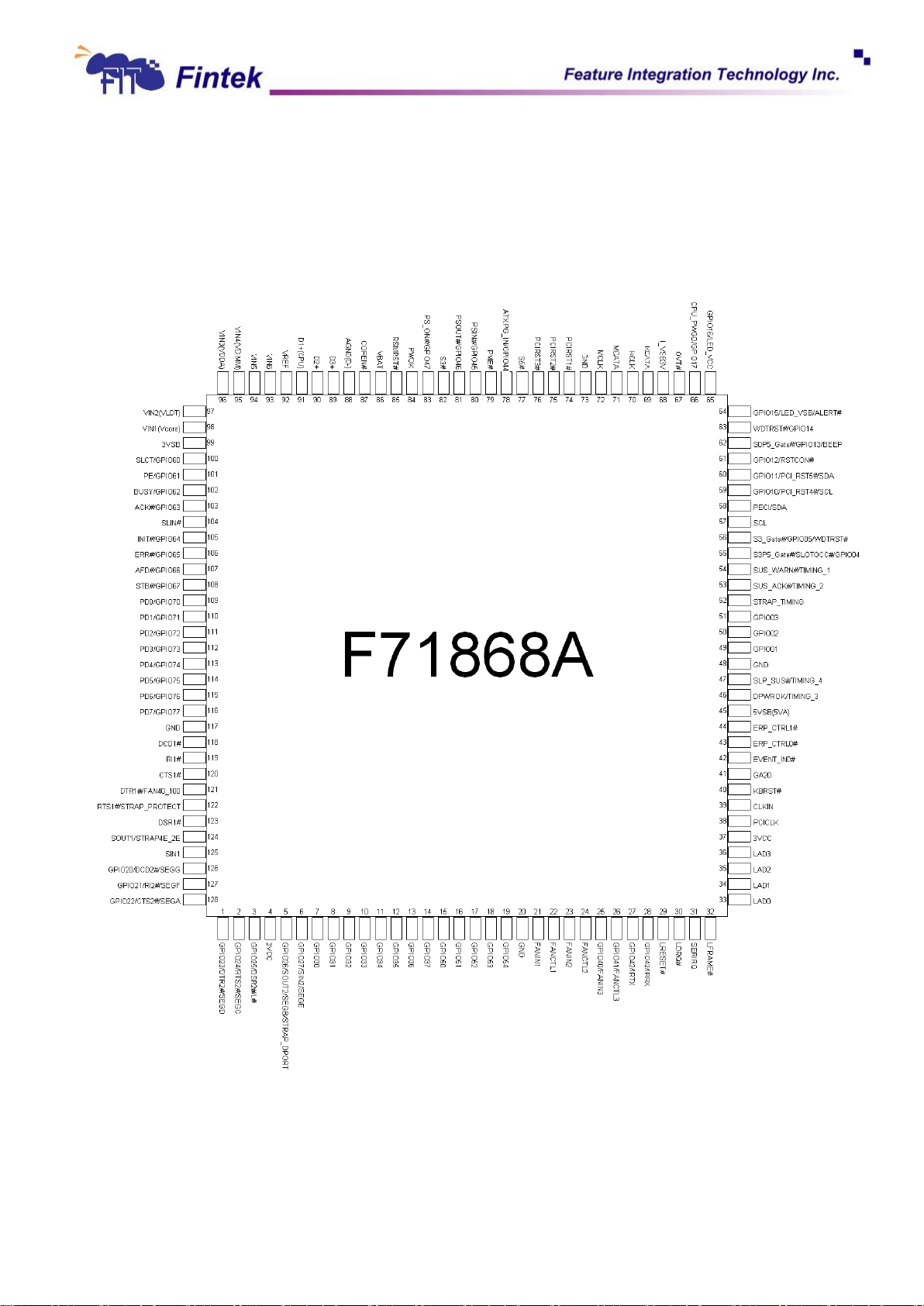
Figure1. F71868A pin configuration (14 *14)
May, 2015
V 0.17P
Page 16
16
F71868A
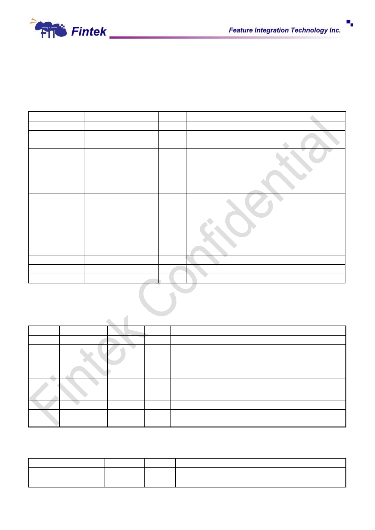
4. Pin Description
Pin No.
Pin Name
Type
Description
4,37
3VCC
P
Power supply voltage input with 3.3V (Support OVP)
45
5VSB(5VA)
P
5V stand by power input. Nomally the 5V stand by
power source is from ATX Power directly.
68
I_VSB3V
P
3.3V internal standby power pin which regulates from
5VSB (V5A).
This pin can be an output pin which could provide the
small amount of the current at 5VSB (V5A) existence
for extending the battery life.
86
VBAT
P
Battery voltage input/output pin.
This pin can be an input pin when 5VSB (V5A) does
not exist.
This pin can be an output pin which could provide the
small amount of the current at 5VSB (V5A) existence
for extending the battery life. At the output pin stage,
VBAT voltage detection function is invalid.
88
AGND(D-)
P
Analog GND
99
3VSB
P
Analog Stand-by power supply voltage input 3.3V
20, 48, 73, 117
GND
P
Digital GND
Pin No.
Pin Name
Type
PWR
Description
29
LRESET#
IN
st,5v
3VCC
Reset signal. It can connect to PCIRST# signal on the host.
30
LDRQ#
O16
3VCC
Encoded DMA Request signal.
31
SERIRQ
I/O
16t
3VCC
Serial IRQ input/Output.
32
LFRAME#
INst
3VCC
Indicates start of a new cycle or termination of a broken
cycle.
33-36
LAD[0:3]
I/O16
3VCC
These signal lines communicate address, control, and data
information over the LPC bus between a host and a
peripheral.
38
PCICLK
IN
st,5v
3VCC
33MHz PCI clock input.
39
CLKIN
IN
st,5v
3VCC
System clock input. According to the input frequency
24/48MHz.
Pin No.
Pin Name
Type
PWR
Description
27
GPIO42
I/OOD
12t,5v
3VCC
Default General Purpose IO.
IRTX
O12
Infrared Transmitter Output. The function is selected by
4.1 Power Pins
4.2 LPC Interface
4.3 UART and SIR
May, 2015
V 0.17P
Page 17
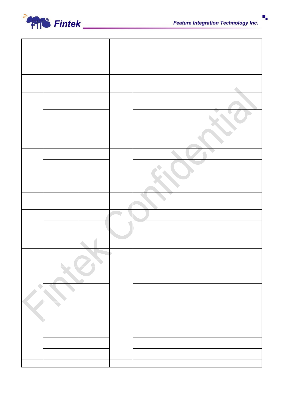
17
F71868A
register setting.
28
GPIO43
I/OOD
12t,5v
3VCC
Default General Purpose IO.
IRRX
IN
st,5v
Infrared Receiver input. The function is selected by register
setting.
118
DCD1#
IN
st,5v
3VCC
Data Carrier Detect. An active low signal indicates the
modem or data set has detected a data carrier.
119
RI1#
IN
st,5v
I_VSB3V
Ring Indicator. An active low signal indicates that a ring
signal is being received from the modem or data set.
120
CTS1#
IN
st,5v
3VCC
Clear To Send is the modem control input.
121
DTR1#
O
8t,5v
3VCC
UART 1 Data Terminal Ready. An active low signal informs
the modem or data set that controller is ready to
communicate.
FAN40_100
IN
t5v,u47k
Internal 47k ohms pulled high and disable after power on
strapping.
Power on strapping pin:
1(Default): (Internal pull high)
Power on fan speed default duty is 40%.(PWM)
0: (External pull down)
Power on fan speed default duty is 100%.(PWM)
122
RTS1#
O
8t,5v
3VCC
UART 1 Request To Send. An active low signal informs the
modem or data set that the controller is ready to send data.
STRAP_PRO
TECT
IN
t5v,u47k
Internal 47k ohms pulled high and disable after power on
strapping.
Power on Strapping pin for over voltage protection function.
1: Default is alarm mode. Voltage protection function is
enabled via setting the related register.
0: Force mode (disabled).
123
DSR1#
IN
st,5v
3VCC
Data Set Ready. An active low signal indicates the modem
or data set is ready to establish a communication link and
transfer data to the UART.
124
SOUT1
O
8t,5v
3VCC
UART 1 Serial Output. Used to transmit serial data out to
the communication link.
STRAP4E_2E
IN
t5v,u47k
Internal 47k ohms pulled high and disable after power on
strapping.
Power on strapping:
1(Default): Configuration register 4E
0: Configuration register 2E
125
SIN1
IN
st,5v
3VCC
Serial Input. Used to receive serial data through the
communication link.
126
GPIO20
I/OOD
12st,5v
3VCC
Default General Purpose IO.
DCD2#
IN
st,5v
Data Carrier Detect. An active low signal indicates the
modem or data set has detected a data carrier.
The function is selected by register setting.
SEGG
O18
SEGG for 7-segment display. (Select by pin 5 power on
strapping)
127
GPIO21
I/OOD
12st,5v
3VCC
Default General Purpose IO.
RI2#
IN
st,5v
Ring Indicator. An active low signal indicates that a ring
signal is being received from the modem or data set.
The function is selected by register setting.
SEGF
O18
SEGF for 7-segment display. (Select by pin 5 power on
strapping)
128
GPIO22
I/OOD
12st,5v
3VCC
Default General Purpose IO.
CTS2#
IN
st,5v
Clear To Send is the modem control input.
The function is selected by register setting.
SEGA
O18
SEGA for 7-segment display. (Select by pin 5 power on
strapping)
1
GPIO23
I/OOD
12st,5v
3VCC
Default General Purpose IO.
May, 2015
V 0.17P
Page 18
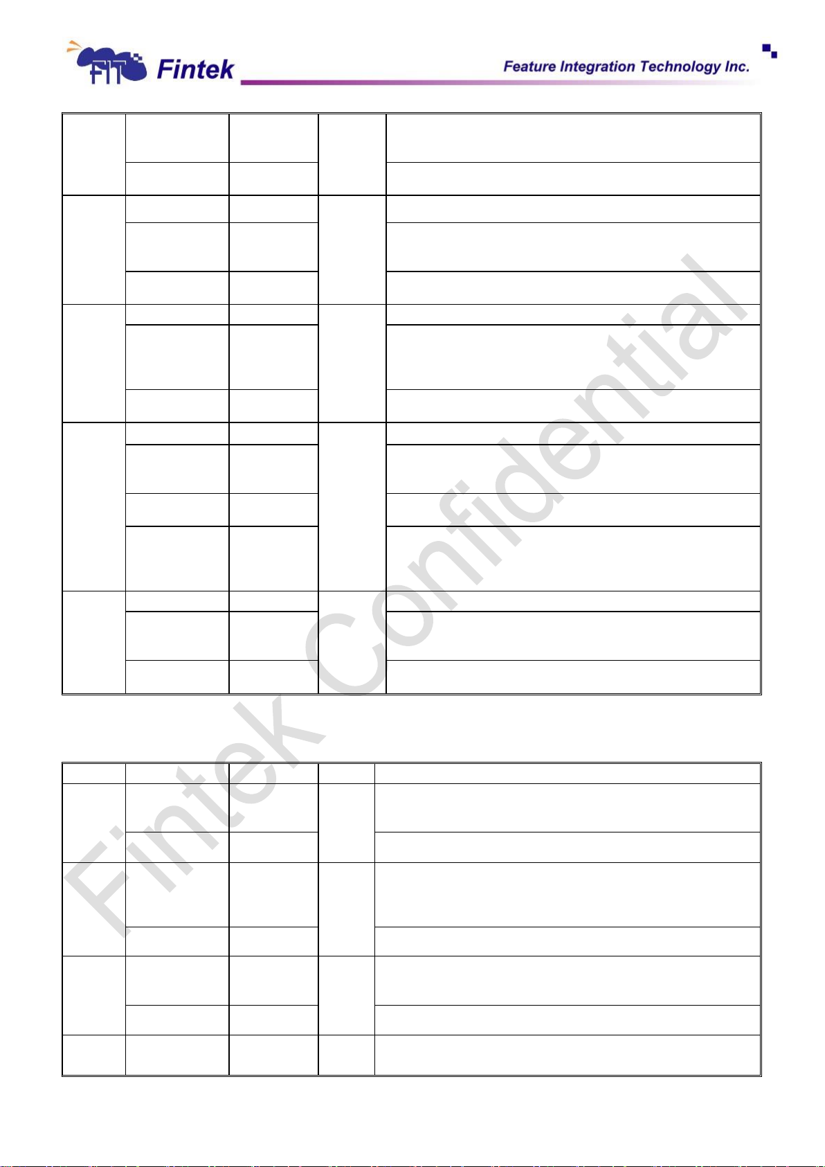
18
F71868A
DTR2#
O
8t,5v
UART 2 Data Terminal Ready. An active low signal informs
the modem or data set that controller is ready to
communicate. The function is selected by register setting.
SEGD
O18
SEGD for 7-segment display. (Select by pin 5 power on
strapping)
2
GPIO24
I/OOD
12st,5v
3VCC
Default General Purpose IO.
RTS2#
O
8t,5v
UART 2 Request To Send. An active low signal informs the
modem or data set that the controller is ready to send data.
The function is selected by register setting.
SEGC
O18
SEGC for 7-segment display. (Select by pin 5 power on
strapping)
3
GPIO25
I/OOD
12st,5v
3VCC
Default General Purpose IO.
DSR2#
IN
st,5v
Data Set Ready. An active low signal indicates the modem
or data set is ready to establish a communication link and
transfer data to the UART. The function is selected by
register setting.
L#
O30
L# for 7-segment display. (Select by pin 5 power on
strapping)
5
GPIO26
I/OOD
12st,5v
3VCC
Default General Purpose IO.
SOUT2
O
8t,5v
UART 2 Serial Output. Used to transmit serial data out to
the communication link. The function is selected by register
setting.
SEGB
O18
SEGB for 7-segment display. (Select by pin 5 power on
strapping)
STRAP_DPORT
IN
t5v,u47k
Internal 47k ohms pulled high and disable after power on
strapping.
Strap for 80 Port. Default internal Pull High for 80 Port
Enable.
6
GPIO27
I/OOD
12st,5v
3VCC
Default General Purpose IO.
SIN2
IN
st,5v
Serial Input. Used to receive serial data through the
communication link. The function is selected by register
setting.
SEGE
O18
SEGE for 7-segment display. (Select by pin 5 power on
strapping)
Pin No.
Pin Name
Type
PWR
Description
100
SLCT
IN
st,5v
3VCC
An active high input on this pin indicates that the printer is
selected. Refer to the description of the parallel port for
definition of this pin in ECP and EPP mode.
GPIO60
I/OOD
12t,5v
Default General Purpose IO.
101
PE
IN
st,5v
3VCC
An active high input on this pin indicates that the printer has
detected the end of the paper. Refer to the description of the
parallel port for the definition of this pin in ECP and EPP
mode.
GPIO61
I/OOD
12t,5v
Default General Purpose IO.
102
BUSY
IN
st,5v
3VCC
An active high input indicates that the printer is not ready to
receive data. Refer to the description of the parallel port for
definition of this pin in ECP and EPP mode.
GPIO62
I/OOD
12t,5v
Default General Purpose IO.
103
ACK#
IN
st,5v
3VCC
An active low input on this pin indicates that the printer has
received data and is ready to accept more data. Refer to the
4.4 Parallel Port
May, 2015
V 0.17P
Page 19
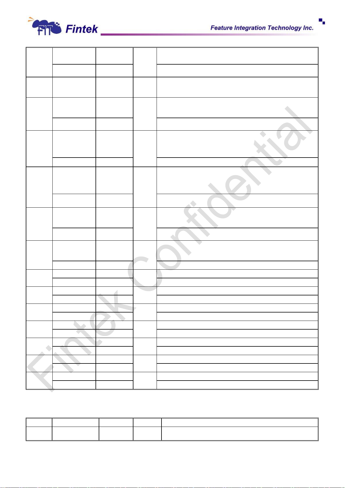
19
F71868A
description of the parallel port for the definition of this pin in
ECP and EPP mode.
GPIO63
I/OOD
12t,5v
Default General Purpose IO.
104
SLIN#
I/OOD
12st,5v
3VCC
Output line for detection of printer selection. Refer to the
description of the parallel port for the definition of this pin in
ECP and EPP mode.
105
INIT#
I/OOD
12st,5v
3VCC
Output line for the printer initialization. Refer to the
description of the parallel port for the definition of this pin in
ECP and EPP mode.
GPIO64
I/OOD
12t,5v
Default General Purpose IO.
106
ERR#
IN
st,5v
3VCC
An active low input on this pin indicates that the printer has
encountered an error condition. Refer to the description of
the parallel port for the definition of this pin in ECP and EPP
mode.
GPIO65
I/OOD
12t,5v
Default General Purpose IO.
107
AFD#
I/OOD
12st,5v
3VCC
An active low output from this pin causes the printer to auto
feed a line after a line is printed. Refer to the description of
the parallel port for the definition of this pin in ECP and EPP
mode.
GPIO66
I/OOD
12t,5v
Default General Purpose IO.
108
STB#
I/OOD
12st,5v
3VCC
An active low output is used to latch the parallel data into the
printer. Refer to the description of the parallel port for the
definition of this pin in ECP and EPP mode.
GPIO67
I/OOD
12t,5v
Default General Purpose IO.
109
PD0
I/O
12st,5v
3VCC
Parallel port data bus bit 0. Refer to the description of the
parallel port for the definition of this pin in ECP and EPP
mode.
GPIO70
I/OOD
12t,5v
Default General Purpose IO.
110
PD1
I/O
12st,5v
3VCC
Parallel port data bus bit 1.
GPIO71
I/OOD
12t,5v
Default General Purpose IO.
111
PD2
I/O
12st,5v
3VCC
Parallel port data bus bit 2.
GPIO72
I/OOD
12t,5v
Default General Purpose IO.
112
PD3
I/O
12st,5v
3VCC
Parallel port data bus bit 3.
GPIO73
I/OOD
12t,5v
Default General Purpose IO.
113
PD4
I/O
12st,5v
3VCC
Parallel port data bus bit 4.
GPIO74
I/OOD
12t,5v
Default General Purpose IO.
114
PD5
I/O
12st,5v
3VCC
Parallel port data bus bit 5.
GPIO75
I/OOD
12t,5v
Default General Purpose IO.
115
PD6
I/O
12st,5v
3VCC
Parallel port data bus bit 6.
GPIO76
I/OOD
12t,5v
Default General Purpose IO.
116
PD7
I/O
12st,5v
3VCC
Parallel port data bus bit 7.
GPIO77
I/OOD
12t,5v
Default General Purpose IO.
Pin No.
Pin Name
Type
PWR
Description
93
VIN6
AIN
I_VSB3V
Voltage input 6. This pin support OVP function, and default
is disable.
4.5 Hardware Monitor
May, 2015
V 0.17P
Page 20
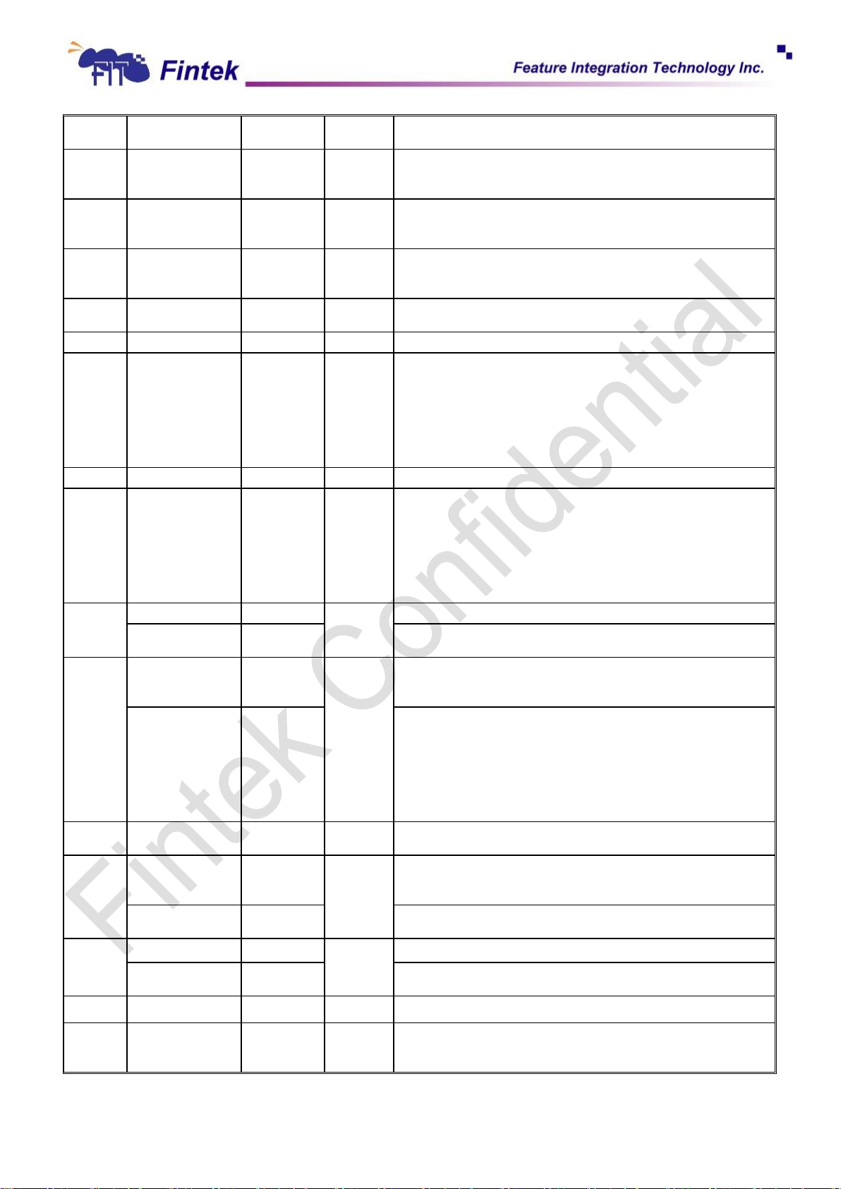
20
F71868A
94
VIN5
AIN
I_VSB3V
Voltage input 5. This pin support OVP function, and default
is disable.
95
VIN4 (VDIMM)
AIN
I_VSB3V
Voltage input 4 or VDIMM input used in AMD platform. The
input voltage level for timing control usage must be over 1V
after voltage divider.
96
VIN3 (VDDA)
AIN
I_VSB3V
Voltage input 3 or VDDA input used in AMD platform. The
input voltage level for timing control usage must be over 1V
after voltage divider.
97
VIN2 (VLDT)
AIN
I_VSB3V
Voltage input 2 or VLDT input used in AMD platform. The
input voltage level for timing control usage must be over 1V
after voltage divider.
98
VIN1 (Vcore)
AIN
I_VSB3V
Voltage Input for Vcore. The input voltage level for timing
control usage must be over 0.7V.
21
FANIN1
IN
st,5v
3VCC
Fan 1 tachometer input.
22
FANCTL1
OOD
12,5v
AOUT
3VCC
Fan 1 control output. It is also a trap pin to select a PWM or
a DAC output, except being an output pin. It defaults to be
a voltage output by pulling down 100k internally. It is set as
a PWM output as connected a 4.7K resistor and pulled
high to 3.3V.
The PWM output frequency can be programmed to 220Hz
for LCD backlight control.
23
FANIN2
IN
st,5v
3VCC
Fan 2 tachometer input.
24
FANCTL2
OOD
12,5v
AOUT
3VCC
Fan 2 control output. It is also a trap pin to select a PWM or
a DAC output, except being an output pin. It defaults to be
a voltage output by pulling down 100k internally. It is set as
a PWM output as connected a 4.7K resistor and pulled
high to 3.3V.
The PWM output frequency can be programmed to 220Hz
for LCD backlight control.
25
GPIO40
I/OOD
12st,5v
3VCC
Default General Purpose IO.
FANIN3
IN
st,5v
Fan 3 speed input. This function is selected by register
setting.
26
GPIO41
I/OOD
12st,5v
3VCC
Default General Purpose IO. This pin default function is
GPIO function. Please take care of the application if user
wants to implement FANCTL function.
FANCTL3
OOD
12,5v
AOUT
Fan 3 control output. It is also a trap pin to select a PWM or
a DAC output, except being an output pin. It defaults to be
a voltage output by pulling down 100k internally. It is set as
a PWM output as connected a 4.7K resistor and pulled
high to 3.3V.
The PWM output frequency can be programmed to 220Hz
for LCD backlight control.
57
SCL
ILv/OD
12st,5v
I_VSB3V
SMBUS Interface CLOCK pin. Clock output for AMD TSI &
Intel PCH (IBX Peak).
58
PECI
ILv/O
D8,S1
I_VSB3V
Intel PECI hardware monitor interface. When
TIMING_GPIO pin is set in GPIO function (INTEL mode).
PECI function can be set by the register.
SDA
ILv/OD
12st,5v
SMBUS Interface DATA pin. AMD TSI & Intel PCH (IBX
Peak) data pin.
63
WDTRST#
OD
12,5v
I_VSB3V
Watch dog timer signal output.
GPIO14
I/OOD
12st,5v
General Purpose IO. GPIO function is selected by register
setting
67
OVT#
OD
12,5v
I_VSB3V
Over temperature signal output.
79
PME#
OD
12,5v
I_VSB3V
Generated PME event. It supports the PCI PME# interface.
This signal allows the peripheral to request the system to
wake up from the S3 state.
May, 2015
V 0.17P
Page 21
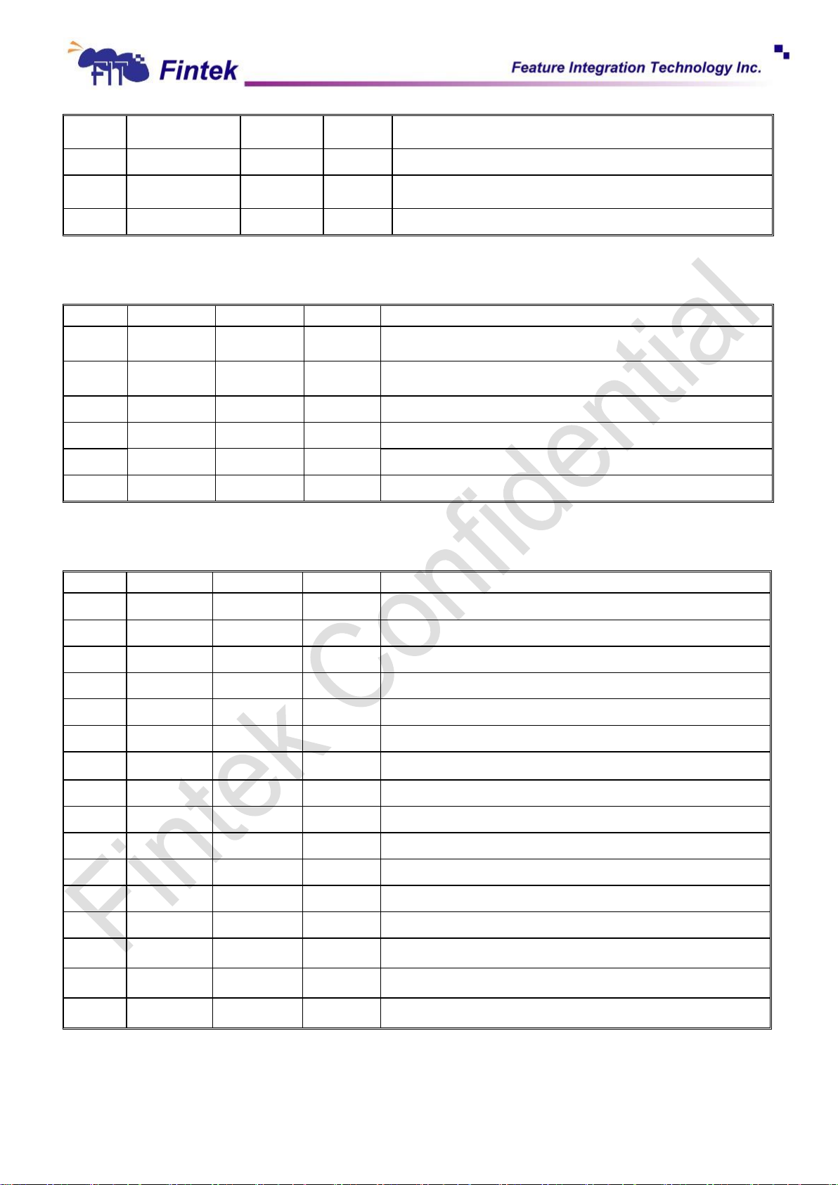
21
F71868A
89
D3+
AIN
I_VSB3V
Thermal diode/transistor temperature sensor input for
system use.
90
D2+
AIN
I_VSB3V
Thermal diode/transistor temperature sensor input.
91
D1+(CPU)
AIN
I_VSB3V
CPU thermal diode/transistor temperature sensor input.
This pin is for CPU use.
92
VREF
AOUT
I_VSB3V
Voltage sensor output.
Pin No.
Pin Name
Type
PWR
Description
40
KBRST#
OD
16,5v,u10k
3VCC
Keyboard reset. This pin is high after system reset. Internal
pull high 3.3V with 10k ohms. (KBC P20)
41
GA20
OD
16,5v,u10k
3VCC
Gate A20 output. This pin is high after system reset. Internal
pull high 3.3V with 10k ohms. (KBC P21)
69
KDATA
I/OD
16st,5V
I_VSB3V
Keyboard Data.
70
KCLK
I/OD
16st,5V
I_VSB3V
Keyboard Clock.
71
MDATA
I/OD
16st,5V
I_VSB3V
PS2 Mouse Data.
72
MCLK
I/OD
16st,5V
I_VSB3V
PS2 Mouse Clock.
Pin No.
Pin Name
Type
PWR
Description
7
GPIO30
I/OD
14st,5v
3VCC
Default General Purpose IO.
8
GPIO31
I/OD
14st,5v
3VCC
Default General Purpose IO.
9
GPIO32
I/OD
14st,5v
3VCC
Default General Purpose IO.
10
GPIO33
I/OD
14st,5v
3VCC
Default General Purpose IO.
11
GPIO34
I/OD
14st,5v
3VCC
Default General Purpose IO.
12
GPIO35
I/OD
14st,5v
3VCC
Default General Purpose IO.
13
GPIO36
I/OD
14st,5v
3VCC
Default General Purpose IO.
14
GPIO37
I/OD
14st,5v
3VCC
Default General Purpose IO.
15
GPIO50
I/OD
12st,5v
3VCC
Default General Purpose IO.
16
GPIO51
I/OD
12st,5v
3VCC
Default General Purpose IO.
17
GPIO52
I/OD
12st,5v
3VCC
Default General Purpose IO.
18
GPIO53
I/OD
12st,5v
3VCC
Default General Purpose IO.
19
GPIO54
I/OD
12st,5v
3VCC
Default General Purpose IO.
49
GPIO01
I/OOD
12t
I_VSB3V
Default General Purpose IO.
50
GPIO02
I/OOD
12t
I_VSB3V
Default General Purpose IO.
51
GPIO03
I/OOD
12t
I_VSB3V
Default General Purpose IO.
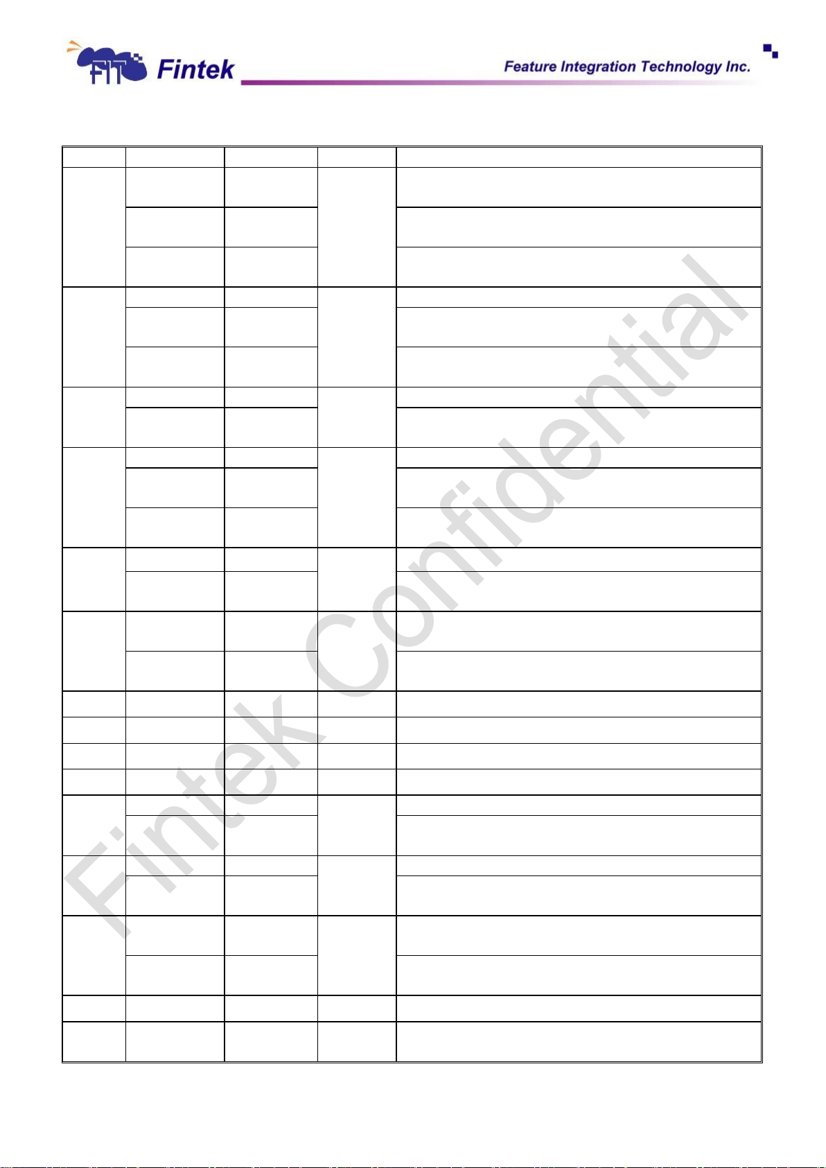
4.6 KBC Function
4.7 GPIO
May, 2015
V 0.17P
Page 22
22
F71868A
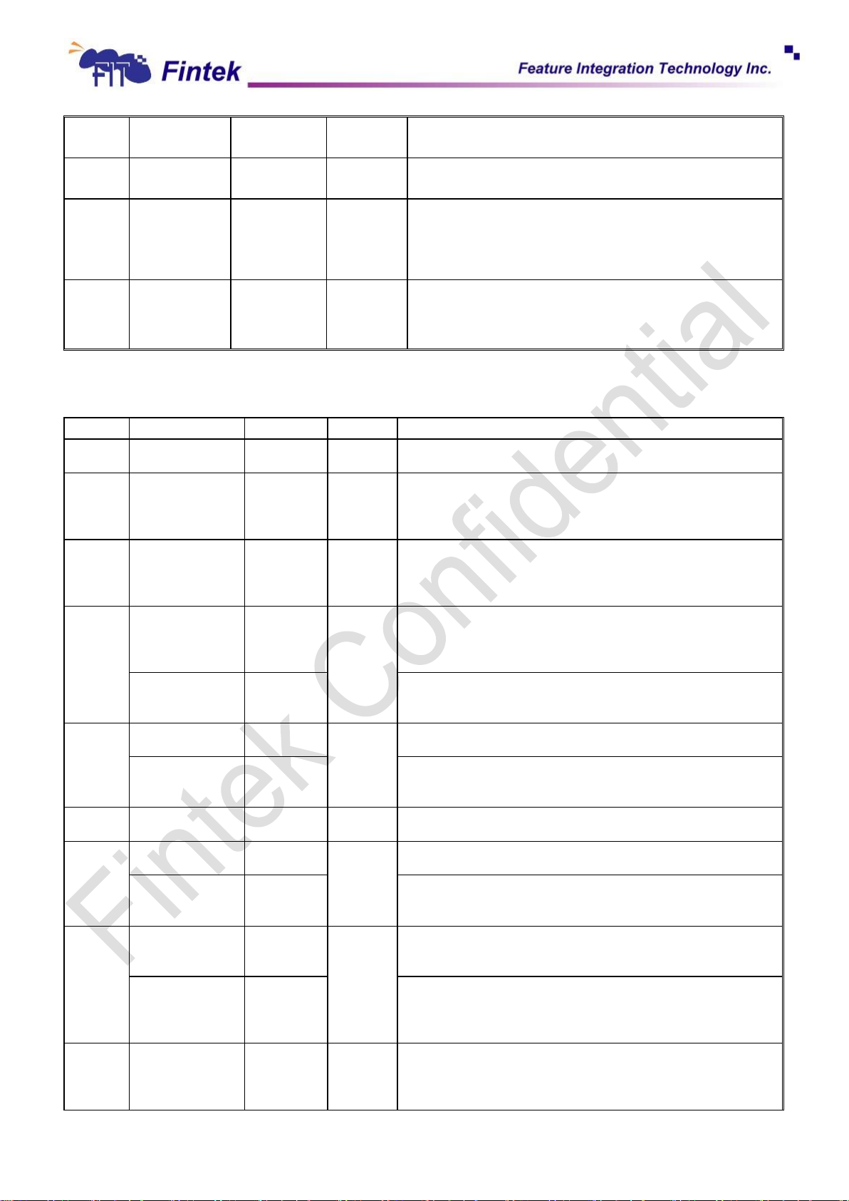
4.8 ACPI Function Pins
Pin No.
Pin Name
Type
PWR
Description
59
GPIO10
I/OOD
12st,5v
I_VSB3V
Default General Purpose IO. GPIO function is selected
by register setting
PCI_RST4#
O
12,5v
It is an output buffer of LRESET#. This function is
selected by register setting.
SCL
ILv /OD
12st,5v
SMBUS Interface CLOCK pin. Clock output for AMD TSI &
Intel PCH (IBX Peak).
60
GPIO11
I/OOD
12st,5v
I_VSB3V
Default General Purpose IO.
PCI_RST5#
O
12,5v
It is an output buffer of LRESET#. This function is
selected by register setting.
SDA
ILv /OD
12st,5v
SMBUS Interface DATA pin. AMD TSI & Intel PCH (IBX
Peak) data pin.
61
GPIO12
I/OOD
12st,5v
I_VSB3V
Default General Purpose IO.
RSTCON#
IN
st,5v
Reset button input. This function is selected by register
setting.
64
GPIO15
I/OOD
12st,5v
I_VSB3V
Default General Purpose IO.
LED_VSB
OD
12,5v
Power LED for VSB. This function is selected by register
setting.
ALERT#
OD
12,5v
Alert a signal when temperature over limit setting. This
function is selected by register setting.
65
GPIO16
I/OOD
12st,5v
I_VSB3V
Default General Purpose IO.
LED_VCC
OD
12,5v
Power LED for VCC. This function is selected by register
setting.
66
CPU_PWGD
OD
12,5v
I_VSB3V
CPU Power Good signal output
(Detected by VIN1~VIN4 level good)
GPIO17
I/OOD
12st,5v
General Purpose IO. GPIO function is selected by register
setting
74
PCIRST1#
OD
12,5v
I_VSB3V
It is an output buffer of LRESET#.
75
PCIRST2#
O
12,5v
I_VSB3V
It is an output buffer of LRESET#.
76
PCIRST3#
O
12,5v
I_VSB3V
It is an output buffer of LRESET#.
77
S5#
IN
st,5v
I_VSB3V
S5# signal input.
78
ATXPG_IN
IN
st,5v
I_VSB3V
ATX Power Good input.
GPIO44
I/OOD
12st,5v
General Purpose IO. GPIO function is selected by
register setting.
80
PSIN#
IN
st,5v
I_VSB3V
Main power switch button input.
GPIO45
I/OOD
12st,5v
General Purpose IO. GPIO function is selected by
register setting.
81
PSOUT#
OD
12,5v
I_VSB3V
Panel Switch Output. This pin is low active and pulse
output. It is power on request output#.
GPIO46
I/OOD
12st,5v
General Purpose IO. GPIO function is selected by
register setting.
82
S3#
IN
st,5v
I_VSB3V
S3# Input is Main power on-off switch input.
83
PS_ON#
OD
12,5v
I_VSB3V
Power supply on-off control output. Connect to ATX
power supply PS_ON# signal.
May, 2015
V 0.17P
Page 23
23
F71868A
GPIO47
I/OD
12st,5v
General Purpose IO. GPIO function is selected by
register setting.
84
PWOK
OD
12,5v
VBAT
PWOK function, It is power good signal of VCC, which is
delayed 400ms (default) as VCC arrives at 2.8V.
85
RSMRST#
OD
12,5v,u10k
VBAT
Resume Reset# function, It is power good signal of VSB,
which rises delayed 66ms as VSB arrives at 2.8V and
falls as VSB drops to 2.6V. There is an option to set
RSMRST# rises at 3.05V and falls at 2.95V.
87
COPEN#
IN
st,5v
VBAT
Case Open Detection #. This pin is connected to a
specially designed low power CMOS flip-flop backed by
the battery for case open state preservation during power
loss.
Pin No.
Pin Name
Type
PWR
Description
42
EVENT_IN0#
IN
st, 5v
I_VSB3V
Wake-up event input. The signal input wakes the system
up from the sleep state.
43
ERP_CTRL0#
OD12
I_VSB3V
Standby power rail control pin 0. This pin controls an
external PMOS to turn on or off the standby power rail. In
the S5 state, the default is set to 1 to cut off the standby
power rail.
44
ERP_CTRL1#
OD12
I_VSB3V
Standby power rail control pin 1. This pin controls an
external PMOS to turn on or off the standby power rail. In
the S5 state, the default is set to 1 to cut off the standby
power rail.
46
DPWROK
OD
12,5v
I_VSB3V
Resume Reset# function, It is power good signal of VSB,
which is delayed 66ms as VSB arrives at 4.4V. Couple this
pin to PCH when system supports Intel DSW state
function.
TIMING_3
OD
12,5v
Active high. Timing sequence 3 of power on/off sequence
pins. The external pull high resistor is required.
(Detected by VIN3 level good)
47
SLP_SUS#
IN
st,lv
I_VSB3V
For Intel CPT DSW function. Connect to PCH SLP_SUS
pin.
TIMING_4
OD
12,5v
Active high. Timing sequence 4 of power on/off sequence
pins. The external pull high resistor is required.
(Detected by VIN1 level good)
52
STRAP_TIMING
IN
st,5v
I_VSB3V
Strap Pin for AMD and Intel Cougar Point timing. Internal
pull high with AMD timing (Default).
53
SUS_ACK#
OOD
16,5v
I_VSB3V
This pin must wait SUS_WARN# signal for entering DSW
power state.
TIMING_2
OD
12,5v
Active high. Timing sequence 2 of power on/off sequence
pins. The external pull high resistor is required.
(Detected by VIN4 level good)
54
SUS_WARN#
IN
st,5v
I_VSB3V
This pin asserts low when the PCH is planning to enter the
DSW power state. It can detect 5VDUAL level with delay
setting supported.
TIMING_1
OD
12,5v
Active high. Timing sequence 1 of power on/off sequence
pins. The external pull high resistor is required.
(Output detected by VCCOK(VDDOK) level good, ref
Figure 15 )
55
S3P5_Gate#
OD
12
I_VSB3V
Status Pin2 for S0#/S3#/S5# states application. (Default
function)
In S0# S3P5_Gate# pin status is Tri-state.
In S3# S3P5_Gate # pin status is Low level.
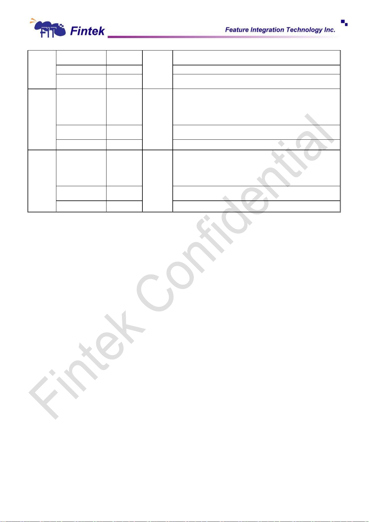
4.9 Power Saving and Others
May, 2015
V 0.17P
Page 24
24
F71868A
In S5# S3P5_Gate # pin status is Tri-state, and can be
programmed Low level.
SLOTOCC#
IN
st,5v
CPU SLOTOCC# input.
GPIO04
OD
12,5v
General Purpose IO. GPIO function is selected by register
setting
56
S3_Gate#
OD12
I_VSB3V
Status Pin1 for S0#/S3#/S5# states application. (Default
function)
In S0# S3_Gate# pin status is Tri-state.
In S3# S3_Gate# pin status is Low level.
In S5# S3_Gate# pin status is Tri-state.
GPIO05
I/OOD
12st,5v
General Purpose IO. GPIO function is selected by register
setting
WDTRST#
OD
12,5v
Watch dog timer signal output.
62
S0P5_Gate#
OD
24,5v
I_VSB3V
S0P5_Gate# for S0#/S3#/S5# states application.
In S0# S0P5_Gate# pin status is Low-state.
In S3# S0P5_Gate# pin status is Tri-state.
In S5# S0P5_Gate# pin status is Tri-state, and can be
programmed Low-state.
GPIO13
I/OOD20st,5v
General Purpose IO. GPIO function is selected by register
setting
BEEP
OD24,5v
Beep pin.
May, 2015
V 0.17P
Page 25
25
F71868A
5. Function Description
Pin No.
Symbol
Value
Description
52
STRAP_TIMING
1
AMD Timing (Default)
0
Intel Cougar Point Timing
121
FAN40_100
1
Power on Fan speed default duty is 40% (PWM)
(Default)
0
Power on Fan speed default duty is 100%(PWM)
124
STRAP4E_2E
1
Configuration Register I/O port is 4E/4F. (Default)
0
Configuration Register I/O port is 2E/2F.
22
FANCTL1
1
FANCTRL1 is PWM mode. Connect a 4.7K resistor
and pull high to 3.3V.
0
FANCTLR1 is DAC mode. (Default)
24
FANCTL2
1
FANCTRL2 is PWM mode. Connect a 4.7K resistor
and pull high to 3.3V.
0
FANCTLR2 is DAC mode. (Default)
26
FANCTL3
1
FANCTRL3 is PWM mode. Connect a 4.7K resistor
and pull high to 3.3V.
0
FANCTLR3 is DAC mode. (Default)
5
STRAP_DPORT
1
Enable 80 Port (Default)
0
Disable 80 Port
122
STRAP_PROTECT
1
Default is alarm mode Voltage protection function is
enabled via setting the related register.
(Enable this function in the OVP start monitor – Index
3Fh)
0
Force mode.
(Default Disabled)
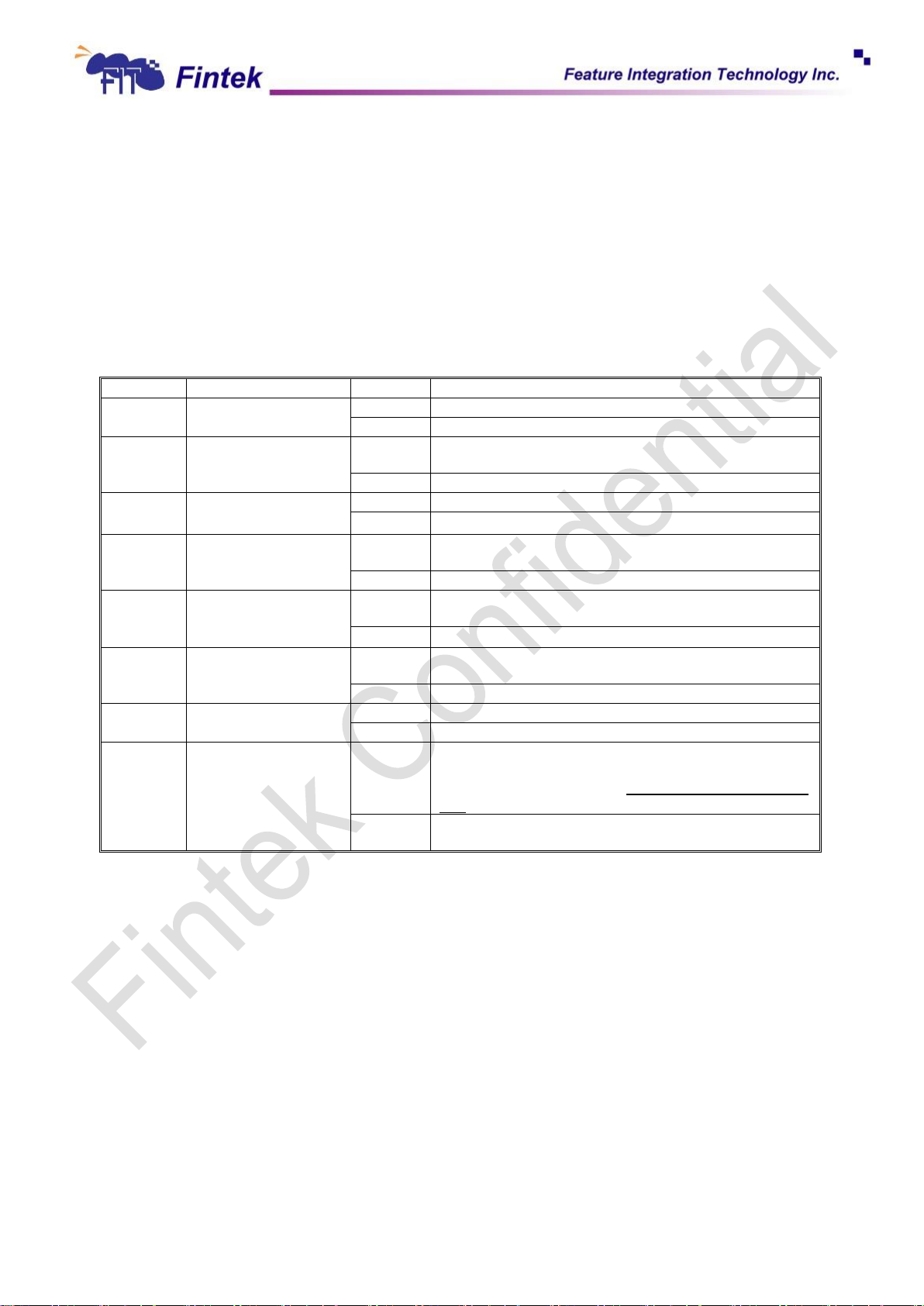
5.1 Power on Strapping Option
The F71868A provides eight pins for power on hardware strapping to select functions. There is a
form to describe how to set the functions you want.
Table1. Power on trap configuration
5.2 Hardware Monitor
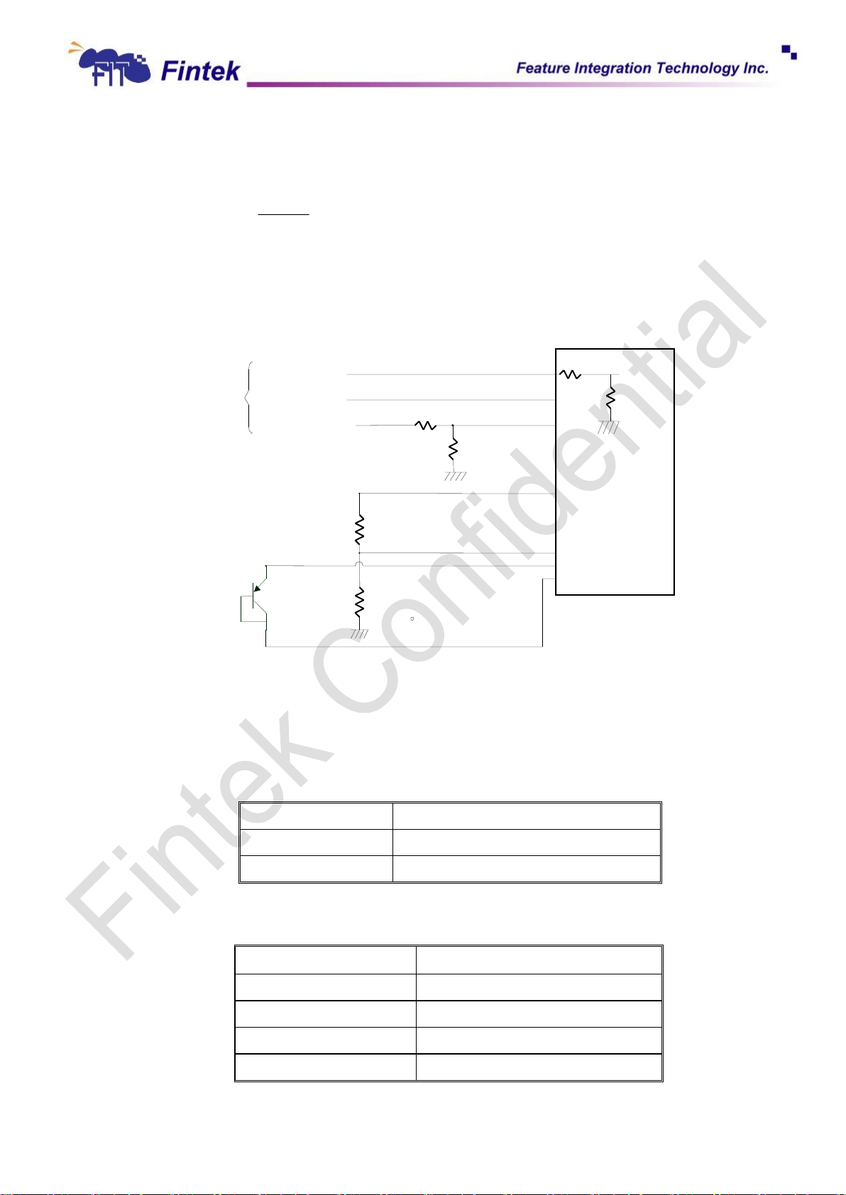
For the 8-bit ADC has the 8mv LSB, the maximum input voltage of the analog pin is 2.048V.
Therefore the voltage under 2.048V (ex: 1.5V) can be directly connected to these analog
inputs. The voltage higher than 2.048V should be reduced by a factor with external resistors
so as to obtain the input range. Only 3VCC/VSB/VBAT is an exception for it is main power of
the F71868A. Therefore 3VCC/VSB/VBAT can directly connect to this chip’s power pin and
need no external resistors. There are two functions in this pin with 3.3V. The first function is to
supply internal analog power of the F71868A and the second function is that voltage with 3.3V
is connected to internal serial resistors to monitor the +3.3V voltage. The internal serial
resistors are two 150K ohm, so that the internal reduced voltage is half of +3.3V.
May, 2015
V 0.17P
Page 26
26
F71868A
21
2
V12
RR
R
VVIN
VIN (Lower than 2.048V)
8-bit ADC
with
8 mV LSB
Voltage Inputs
R1
R2
VIN1(Max2.048V)
VIN(Higher than 2.048V)
(directly connect to the chip)
3VCC/VSB
(directly connect to the chip)
VIN3.3
150K
150K
Typical Thermister
Connection
R
THM
10K, 25 C
R
VREF
10K, 1%
2N3906
Typical BJT
Connection
D+
D-
Manufacturer
Model Number
Panasonic
2SB0709 2N3906
Philips
PMBT3906
Temperature
Digital Output
-40°C
1101 1000
-1°C
1111 1111
1°C
0000 0001
90°C
0101 1010
There are four voltage inputs in the F71868A and the voltage divided formula is shown as
follows:
where V
If we choose R1=27K, R2=5.1K, the exact input voltage for V+12v will be 1.907V, which is
is the analog input voltage, for example.
+12V
within the tolerance. As for application circuit, it can be refer to the figure shown as follows.
Figure 2. Hardware monitor configuration
The F71868A monitors three remote temperature sensors. These sensors can be measured
from -40°C to 127°C. More detail please refer register description.
Table 2. Remote-sensor transistor manufacturers
5.2.1. Table Range:
Table 3. Display range is from -40°C to 127°C in 2’s complement format.
May, 2015
V 0.17P
Page 27

27
F71868A
127°C
1111 1111
Open
1000 0000
5.2.2. Monitor Temperature from “Thermistor”
The F71868A can connect three thermistors to measure environment temperature or
remote temperature. The specification of thermistor should be considered to (1) ß value is
3435K (2) resistor value is 10K ohm at 25ºC. In the Figure 2, the thermistor is connected by a
serial resistor with 10K ohm, then being connected to VREF.
5.2.3. Monitor Temperature from “Thermal diode”
Also, if the CPU, GPU or external circuits provide thermal diode for temperature
measurement, the F71868A is capable to these situations. The build-in reference table is for
PNP 2N3906 transistor. In the Figure 2, the transistor is directly connected into temperature
pins.
5.2.4. ADC Noise Filtering
The ADC is integrating type with inherently good noise rejection. Micro-power operation
places constraints on high-frequency noise rejection; therefore, careful PCB board layout and
suitable external filtering are required for high-accuracy remote measurement in electronically
noisy environment. High frequency EMI is best filtered at D+ and D- with an external 2200pF
capacitor. Too high capacitance may introduce errors due to the rise time of the switched
current source. Nearly all noise sources tested cause the ADC measurement to be higher
than the actual temperature, depending on the frequency and amplitude.
5.2.5. Monitor Temperature from “SMBus device”
F71868A provides SMBus block read/write compatible Platform Control Hub (PCH) EC
SMBus protocol, and provides byte read/write protocol to read CPU and chipset thermal
temperature information. For byte read /write protocol, F71868A supports 4-suit device
address to read or write from device information. For block read/write, F71868A support 1
suits device address and maximum 17 byte count for read protocol to read from device
information, and 4 byte count for write protocol to write information to device.
5.2.6. Monitor Temperature from “PECI”
F71868A support Intel PECI1.1/PECI3.0/PECI_Request/PECI_Available interfaces to read
temperature from PECI device.
May, 2015
V 0.17P
Page 28

28
F71868A
5.2.7. Temperature OVT# Signal
T
HYST
T
OVT#
OVT
t1t2t3
t4
There is a mode of temperature (t1 to t4) OVT function, and refer t1 to t4 temperature in the
below Figure.
Over temperature event will trigger OVT# that shown as figure 3. In hysteresis mode, when
monitored temperature exceeds the high temperature threshold value, OVT# will be asserted
until the temperature goes below the hysteresis temperature.
5.2.8. Temperature PME#
PME# interrupt for temperature is shown as figure 4. Temperature exceeding high limit (low
limit) or going below high hysteresis (low hysteresis) will cause an interrupt if the previous
interrupt has been reset by writing “1” all the interrupt Status Register.
Figure 3
May, 2015
V 0.17P
Page 29

29
F71868A
*Interrupt Reset when Interrupt Status Registers are written 1
PME#
(pulse mode)
* *
T
OVT
T
Hhys
*
*
T
HIGHTHhys
5.2.9. Fan Speed Count
RPM
105.1
Count
6
Count
105.1
RPM
6
Figure 4 Hysteresis mode illustration
Inputs are provided by the signals from fans equipped with tachometer outputs. The level of
these signals should be set to TTL level, and maximum input voltage cannot be over 5V. If the
input signals from the tachometer outputs are over the 5V, the external trimming circuit should
be added to reduce the voltage to obtain the input specification.
Determine the fan counter according to:
In other words, the fan speed counter has been read from register, the fan speed can be
evaluated by the following equation. As for fan, it would be best to use 2 pulses tachometer
output per round.
As the register description of datasheet, the parameter “Count” register provides 12-bit
resolution for RPM counting. In Fintek design, the value of parameter “Count” is from 4096 ~ 64
(5 bit filter). Therefore the RPM measure capability is from 366 ~ 23438 rpm.
Above example is for 2 pulses tachometer (Normal 4 Phases fan) output per round. If you use
8 Phases fan, means output 4 pulses per round. The RPM measure capability is from 183 ~
11719 rpm.
5.2.10. Fan Speed Control
The F71868A provides 2 fan speed control methods: one is DAC FAN control and the other
is PWM duty cycle.
1. DAC Fan Control
May, 2015
V 0.17P
Page 30
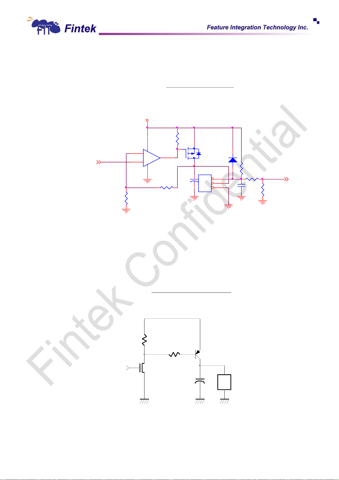
30
F71868A
The range of DC output is 0~3.3V, controlled by 8-bit register. 1 LSB is about 0.013V. The
255
ValueRegister 8bit Programmed
3.3(V) tageOutput_vol
FANIN MONITOR
DC OUTPUT VOLTAGE
+12V
R 10K
1
2
3
JP1
CON3
R
10K
R
3.6K
D1
1N4148
3
2
1
8
4
+
-
U1A
LM358
R 27K
R
4.7K
C
47u
Q1
PMOS
C
0.1u
R
4.7K
%100
255
ValueRegister 8bit Programmed
(%)Duty_cycle
+12V
FANR1R2
NMOS
PNP Transistor
C
+
-
DSG
output DC voltage is amplified by external OP circuit, thus to reach maximum FAN
OPERATION VOLTAGE, 12V. The output voltage will be given as followed:
And the suggested application circuit for DAC fan control would be:
Figure 5 DAC fan control application circuit
2. PWM duty Fan Control
The duty cycle of PWM can be programmed by a 8-bit register. The default duty cycle is set
to 100%, that is, the default 8-bit registers is set to FFh. The expression of duty can be
represented as follows.
Figure 6 +12/5V PWM fan control application circuit
May, 2015
V 0.17P
Page 31
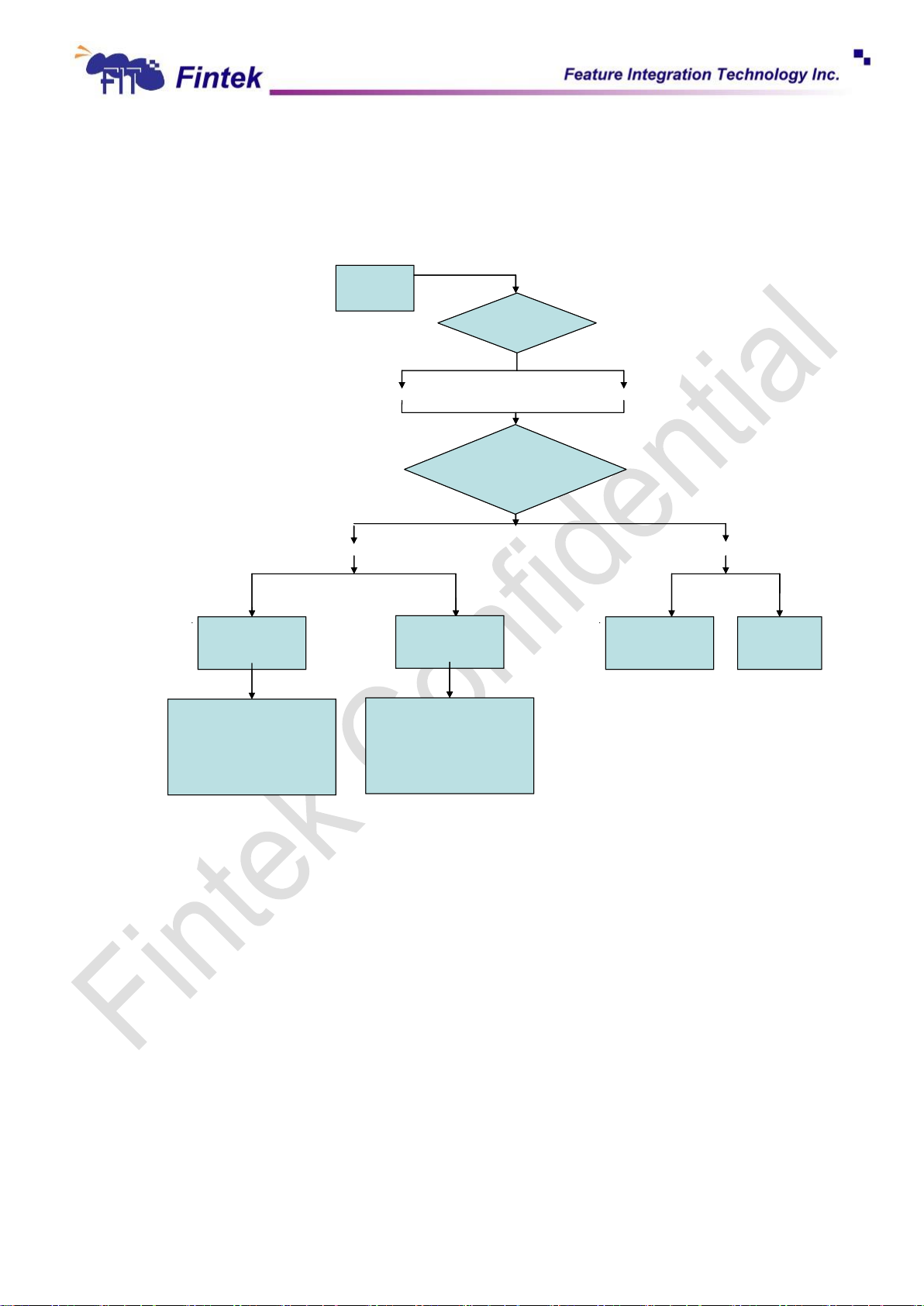
31
F71868A
5.2.11. Fan Speed Control Mechanism
Start
Step1: Select FAN_TYPE
(CR94)
DAC (linear) PWM
Manual ModeAuto Mode
Step2 :Select FAN_MODE
CR96 [5:4] Fan3
CR96 [3:2] Fan2
CR96 [1:0] Fan1
Step3: Set RPM
FAN1 :CR A2,A3
FAN2 :CR B2,B3
FAN3 :CR C2,C3
Step3: Set Duty
FAN1 :CR,A3
FAN2 :CR B3
FAN3 :CR C3
RPM
Duty
Step4: Set H/W Monitor
Fan1 – (BOUNDARY :CR A6~A9)
(SPEED : CR AA ~ AE)
Fan2 –(BOUNDARY :CR B6~B9)
(SPEED : CR BA ~ BE)
Fan3 –(BOUNDARY :CR C6~C9)
(SPEED : CR CA ~ CE)
Step3: Set temp. follows
FAN1 :CRAF
FAN2 :CRBF
FAN3 :CRCF
RPM Duty
Step4: Set H/W Monitor
Fan1 – (BOUNDARY :CR A6~A9)
(SPEED : CR AA ~ AE)
Fan2 –(BOUNDARY :CR B6~B9)
(SPEED : CR BA ~ BE)
Fan3 –(BOUNDARY :CR C6~C9)
(SPEED : CR CA ~ CE)
Step3: Set temp. follows
FAN1 :CRAF
FAN2 :CRBF
FAN3 :CRCF
Start
Step1: Select FAN_TYPE
(CR94)
DAC (linear) PWM
Manual ModeAuto Mode
Step2 :Select FAN_MODE
CR96 [5:4] Fan3
CR96 [3:2] Fan2
CR96 [1:0] Fan1
Step3: Set RPM
FAN1 :CR A2,A3
FAN2 :CR B2,B3
FAN3 :CR C2,C3
Step3: Set Duty
FAN1 :CR,A3
FAN2 :CR B3
FAN3 :CR C3
RPM
Duty
Step4: Set H/W Monitor
Fan1 – (BOUNDARY :CR A6~A9)
(SPEED : CR AA ~ AE)
Fan2 –(BOUNDARY :CR B6~B9)
(SPEED : CR BA ~ BE)
Fan3 –(BOUNDARY :CR C6~C9)
(SPEED : CR CA ~ CE)
Step3: Set temp. follows
FAN1 :CRAF
FAN2 :CRBF
FAN3 :CRCF
RPM Duty
Step4: Set H/W Monitor
Fan1 – (BOUNDARY :CR A6~A9)
(SPEED : CR AA ~ AE)
Fan2 –(BOUNDARY :CR B6~B9)
(SPEED : CR BA ~ BE)
Fan3 –(BOUNDARY :CR C6~C9)
(SPEED : CR CA ~ CE)
Step3: Set temp. follows
FAN1 :CRAF
FAN2 :CRBF
FAN3 :CRCF
There are some modes to control fan speed and they are 1.Manual mode, 2.Stage auto
mode 3. Linear auto mode. Please refer to the figure below. For more detail, please refer the
description of registers.
Figure7 Fan type and mode selection flow
Each fan can be controlled by up to 8 kinds of temperature inputs: (1) D1+ temperature (2)
D2+ temperature (3) D3+ temperature (4) PECI temperature (5) 4 suits SMBus master
temperature. Each fan would make the maximum temperature comparison form those inputs
with the expected speed, and decide the suitable fan speed. Please refer below figure 7.
May, 2015
V 0.17P
Page 32
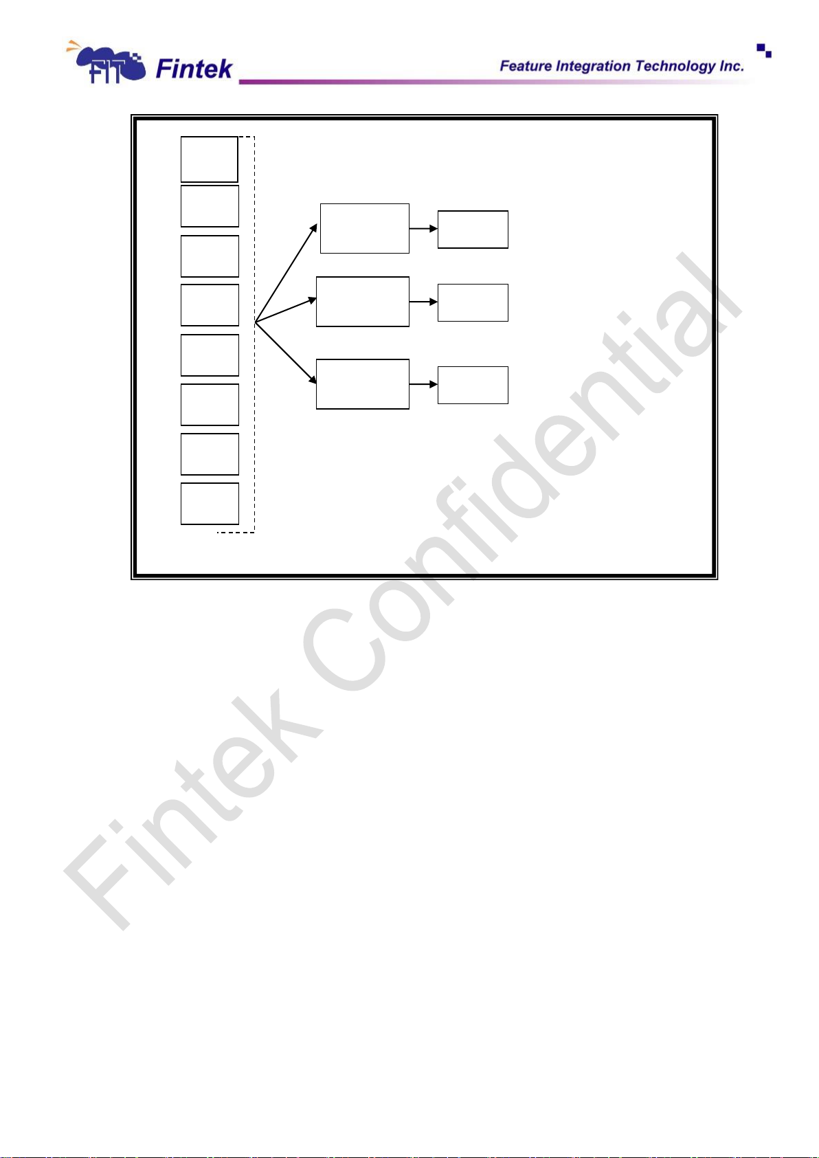
32
F71868A
Expected
speed1
Expected
speed 2
Fan1
Fan2
D2+ T
(T2)
D1+ T
(T1)
PECI
(T0)
D3+ T
(T3)
IBX
Byte1
IBX
Byte3:2
IBX
Byte4
IBX
Byte5
Expeted
speed 3
Fan3
Figure 8 Relative temperature fan control
Manual mode
For manual mode, it generally acts as software fan speed control.
Auto mode
In auto mode, the F71868A provides automatic fan speed control related to temperature variation
of CPU/GPU or the system. The F71868A can provide four temperature boundaries and five intervals,
and each interval has its related fan speed count. All these values should be set by BIOS first. Take
FAN1 for example, the 4 temperature boundaries could be set from register 0xA6 to 0xA9 and the five
intervals for fan speed control could be set from register 0xAA to 0xAE. And the hysteresis setting (0 ~
15°C) could also be found in register 0x98.
The Manual Mode and Auto Mode could be selected by register 0x96h.
There are two kinds of auto mode: stage auto mode and linear auto mode. The “FAN1_
INTERPOLATION_EN” in register 0xAFh is used for linear auto mode enable. The following
examples explain the differences for stage auto mode and linear auto mode.
Stage auto mode
types of fan speed setting: PWM Duty and RPM %.
In this mode, the fan keeps in a same speed for each temperature interval. And there are two
May, 2015
V 0.17P
Page 33
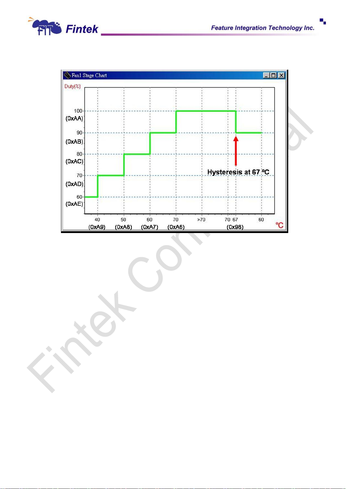
33
F71868A
A. Stage auto mode (PWM Duty)
Set the temperature limits as 70°C, 60°C, 50°C, 40°C and the duty as 100%, 90%, 80%, 70%, 60%
Figure 9 Stage mode fan control illustration-2
a. Once the temperature is under 40°C, the lowest fan speed keeps in the 60% PWM duty.
b. Once the temperature is over 40°C, 50°Cand 60°C, the fan speed will vary from 70%, 80% to 90%
PWM duty and increasing with the temperature level.
c. For the temperature higher than 70°C, the fan speed keeps in 100% PWM duty.
d. If set the hysteresis is 3°C (default 4°C), once the temperature becomes lower than 67°C, the fan
speed would reduce to 90% PWM duty.
May, 2015
V 0.17P
Page 34
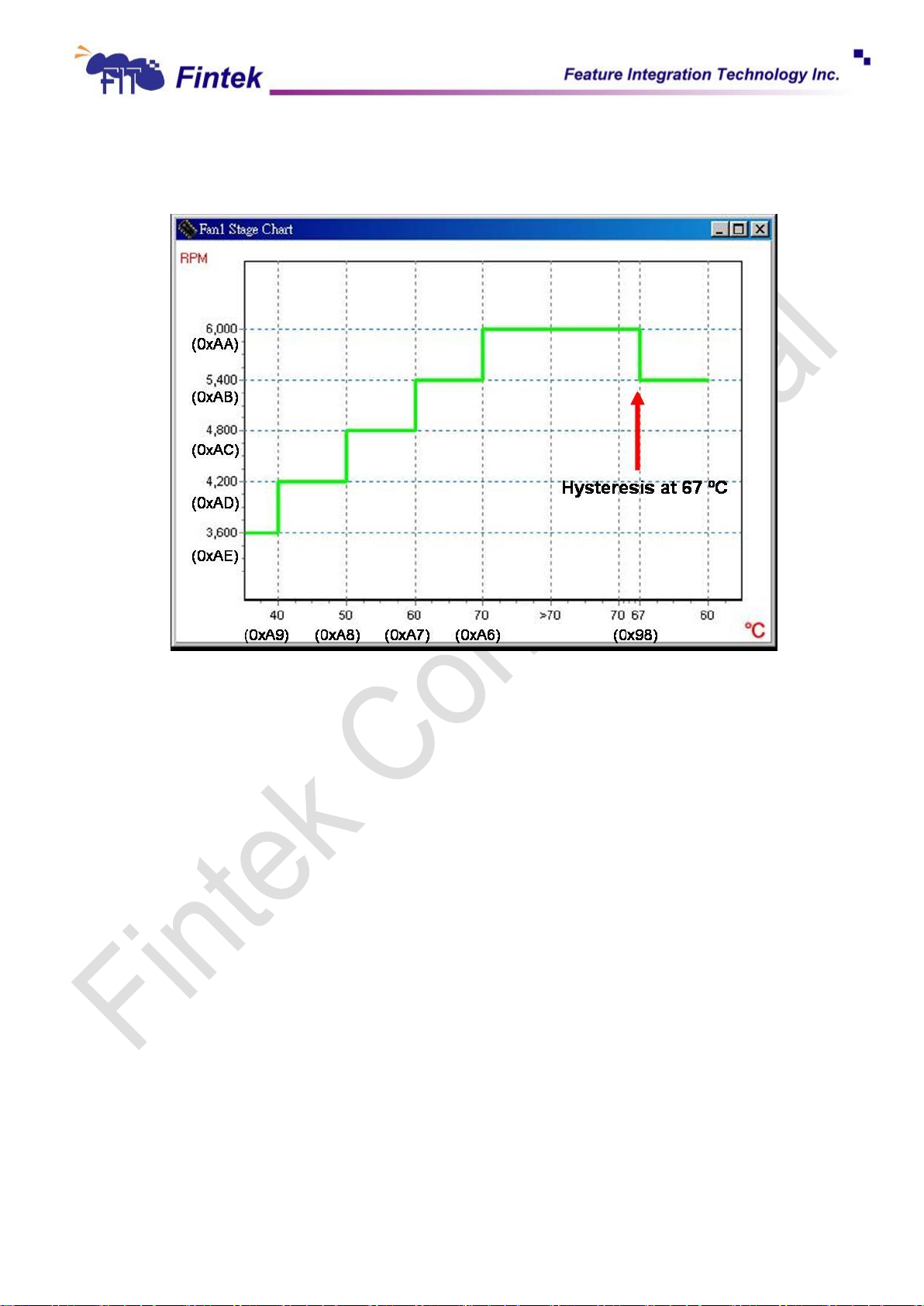
34
F71868A
B. Stage auto mode (RPM%)
Set the temperature as 70°C, 60°C, 50°C, 40°C and the corresponding fan speed is 6,000 rpm,
5,400 rpm, 4,800 rpm, 4,200 rpm, and 3,600 rpm (assume the Max Fan Speed is 6,000 rpm).
Figure 10 Stage mode fan control illustration-3
a. Once the temperature is lower than 40°C, the lowest fan speed keeps in 3,600 rpm (60% of full
speed).
b. Once the temperature is higher than 40°C, 50°C and 60°C, the fan speed will vary from 4,200 rpm
to 5,400 rpm and increasing with the temperature level.
c. For the temperature higher than 70°C, the fan speed keeps in the full speed 6,000 rpm.
d. If the hysteresis is set as 3°C (default 4°C), once temperature gets lower than 67°C, the fan speed
would reduce to 5,400 rpm.
May, 2015
V 0.17P
Page 35
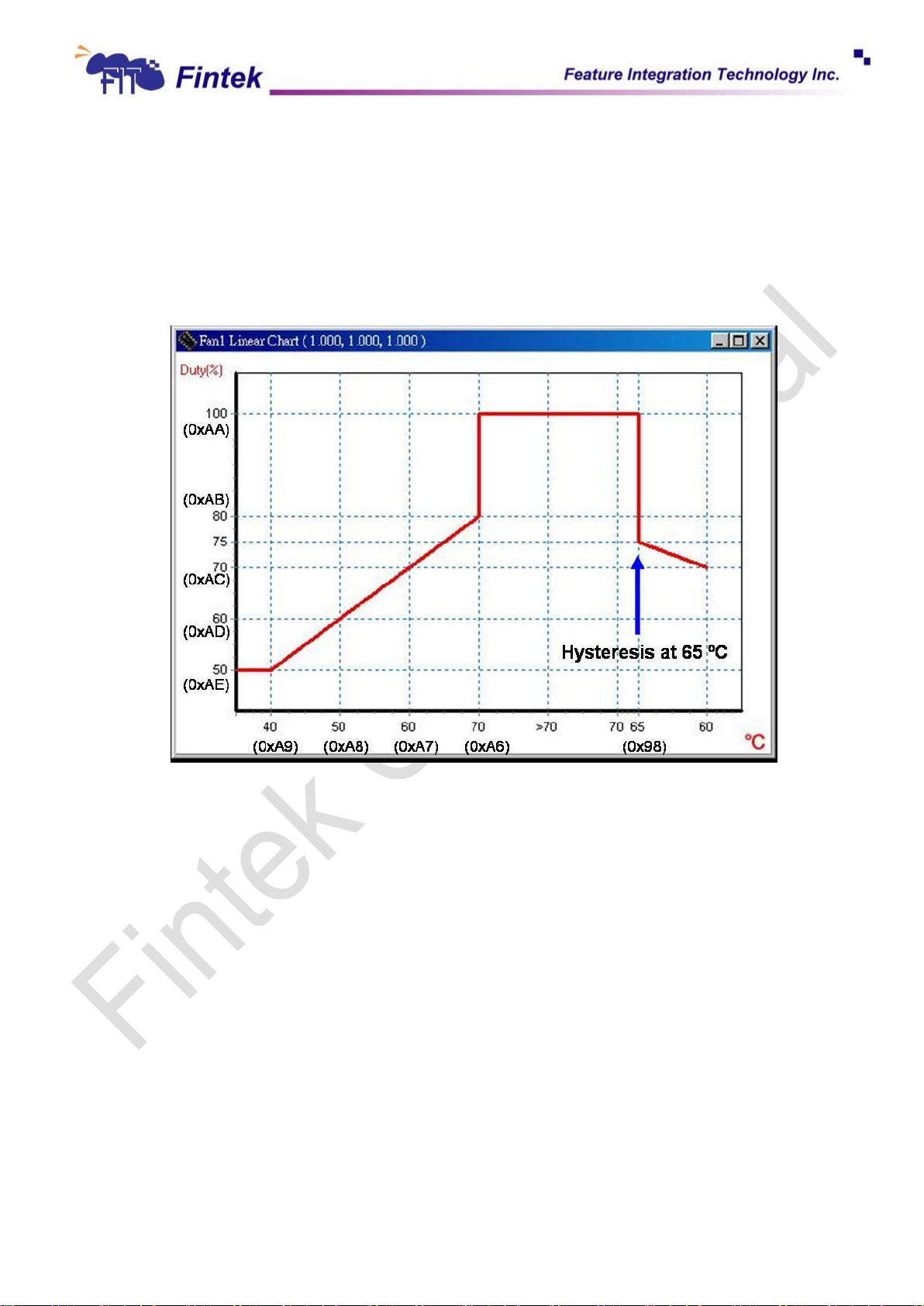
35
F71868A
Linear auto mode
F71868A also supports linear auto mode. The fan speed would increase or decrease linearly with the
temperature. There are also PWM Duty and RPM% modes for it.
A. Linear auto mode (PWM Duty)
Set the temperature as 70°C, 60°C, 50°C and 40°C and the duty is 100%, 80%, 70%, 60% and
50%.
Figure 11 Linear mode fan control illustration-1
a. Once the temperature is lower than 40°C, the lowest fan speed keeps in the 50% PWM duty
b. Once the temperature becomes higher than 40°C, 50°C and 60°C, the fan speed will vary from
50% to 80% PWM duty linearly with the tempreature variation. The temp.-fan speed monitoring
flash interval is 1sec.
c. Once the temperature goes over 70°C, the fan speed will directly increase to 100% PWM duty
(full speed).
d. If set the hysteresis is 5°C (default is 4°C), once the temperature becomes lower than 65°C
(instead of 70°C), the fan speed will reduce from 100% PWM duty and decrease linearly with the
temperature.
May, 2015
V 0.17P
Page 36
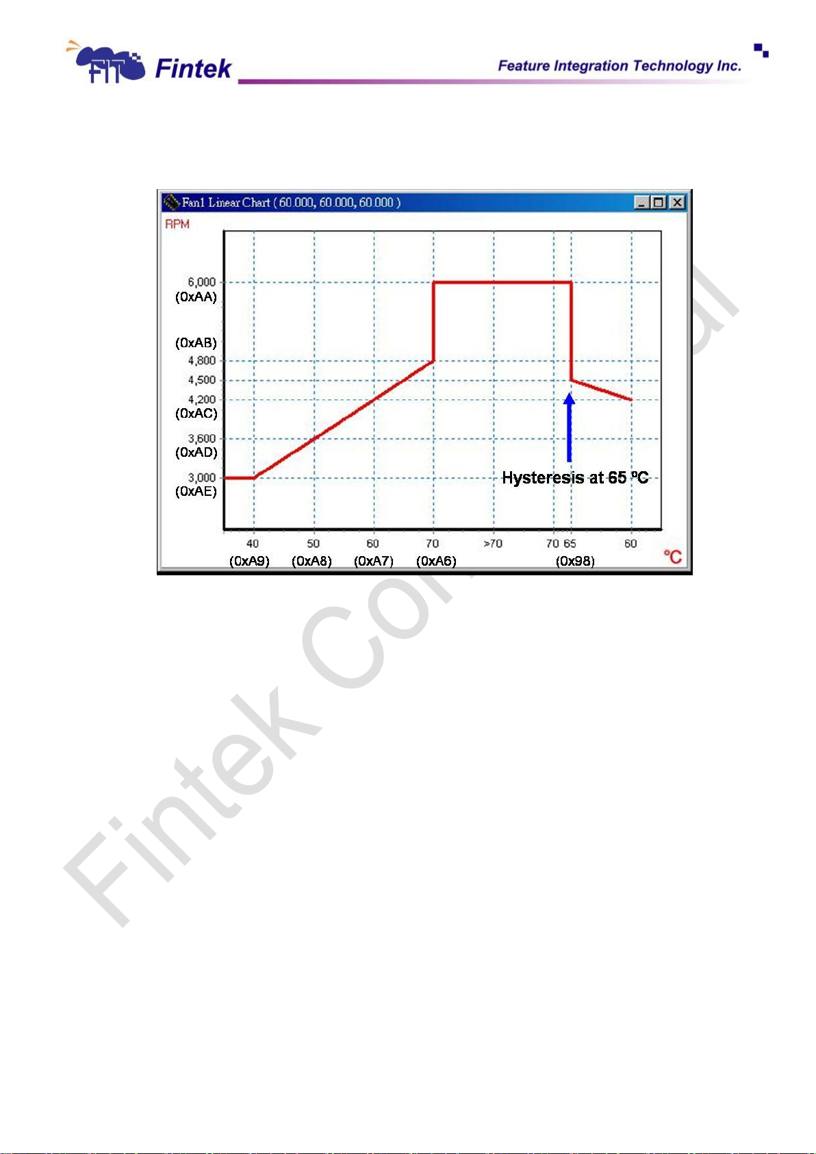
36
F71868A
B. Linear auto mode (RPM%)
Set the temperature as 70°C, 60°C, 50°C, 40°C and the corresponding fan speed is 6,000 rpm,
4,800 rpm, 4,200 rpm, 3,600 rpm and 3,000 rpm (assume the Max Fan Speed is 6,000 rpm).
Figure 12 Linear mode fan control illustration-2
a. Once the temperature is lower than 40°C, the lowest fan speed keeps in 3,000 rpm (50% of full
speed).
b. Once the temperature is over 40°C,50°C and 60°C, the fan speed will vary from 3,000 to 4,800
rpm almost linearly with the temperature variation because the temp.-fan speed monitoring flash
interval is 1sec.
c. Once the temperature goes over 70°C, the fan speed will directly increase to full speed 6,000
rpm.
d. If the hysteresis is 5°C (default is 4°C), once the temperature becomes lower than 65°C (instead
of 70°C), the fan speed wull reduce from full speed and decrease linearly with the temperature.
May, 2015
V 0.17P
Page 37
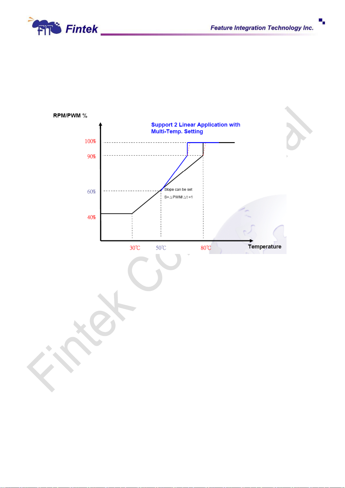
37
F71868A
5.2.12. Fan Speed Control with Multi-temperature.
F71868A supports Multi-temperature for one fan control. This function works with linear
auto mode can extend two linear slopes for one Fan control. As the graph below, this machine
can support more silence fan control in low temperature environment and faster fan speed in
high temperature segment. More detail setting please refers to the registers.
May, 2015
V 0.17P
Page 38
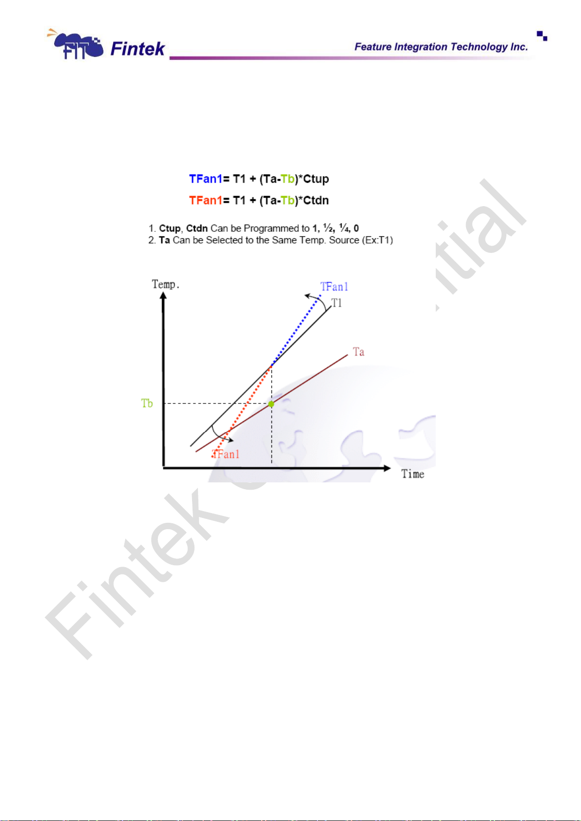
38
F71868A
In the figure below, TFan1 is the scaled temperature for fan1. T1 is the real temperature for
the fan1 sensor. Ta is another temperature data which can be used for linearly scale up or
scale down the fan1 speed curve. Tb would be the point which starts the temperature scaling.
The slope for the temperature curve over and under Tb would be Ctup and Ctdn.
In application, we can set the Ta as the 2nd sensor temperature and Tb as the temperature
which starts the scaling. So if the 2nd sensor temperature Ta is higher or lower than Tb, the
fan1 speed would be changed with it.
May, 2015
V 0.17P
Page 39
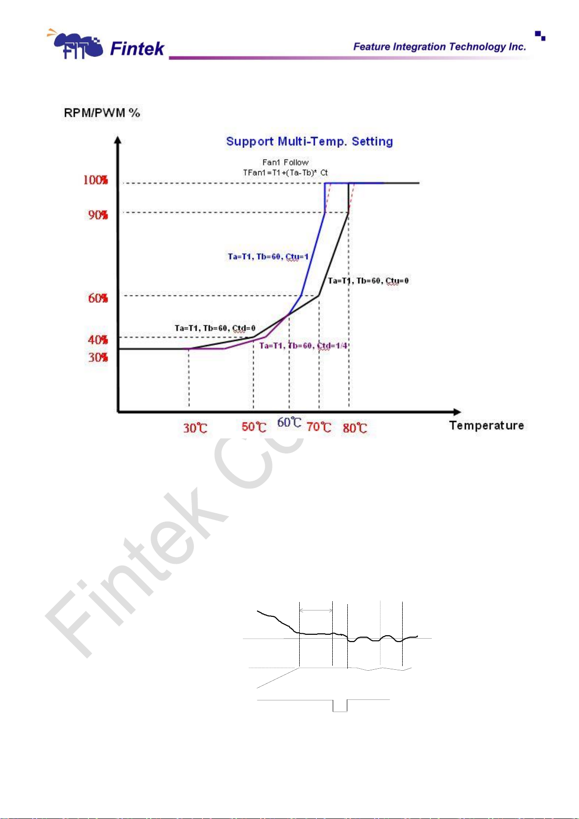
39
F71868A
EX: Ta = T1, Tb = 60, Ctu = 1, Ctd = 1/4
Fan_Fault#
Expected Fan Count
11 sec(default)
Current Fan Count
Duty-cycle
100%
5.2.13. FAN_FAULT#
Fan_Fault# will be asserted when the fan speed doesn’t meet the expected fan speed
within a programmable period (default is 11 seconds) or when fan stops with respect to PWM
duty-cycle which should be able to turn on the fan. There are two conditions may cause the
FAN_FAULT# event.
(1). When PWM_Duty reaches 0xFF, the fan speed count can’t reach the fan expected count
in time.
Figure 13 FAN_FAULT# event
May, 2015
V 0.17P
Page 40

40
F71868A
(2). After the period of detecting fan full speed, PWM_Duty > Min. Duty, fan count is still in
0xFFF.
5.2.14. Over Voltage Protection
F71868A over voltage protection function could protect the damage from voltage spikes via
over voltage & under voltage protection (OVP) function. Hardware strapping pin 122 default is
alarm mode. Voltage protection function is enabled via setting the related register. When force
mode occurs, the system would shut down and then can not boot at all. Only re-plugging the
power code (cut off VSB) could re-activate or re-boot the system at the force mode. Please see
below table for detail information:
May, 2015
V 0.17P
Page 41

41
F71868A
5.3 ACPI Function
VBAT
VSB
RSMRST#
S3#
PS_ON#
PSIN#
PSOUT#
3VCC
G3
S0
The Advanced Configuration and Power Interface (ACPI) is a system for controlling the
use of power in a computer. It lets computer manufacturer and user to determine the computer’s
power usage dynamically.
There are three ACPI states that are of primary concern to the system designer and they are
designated S0, S3 and S5. S0 is a full-power state; the computer is being actively used in this
state. The other two are called sleep states and reflect different power consumption when
power-down. S3 is a state that the processor is powered down but the last procedural state is
being stored in memory which is still active. S5 is a state that memory is off and the last
procedural state of the processor has been stored to the hard disk. Take S3 and S5 as
comparison, since memory is fast, the computer can quickly come back to full-power state, the
disk is slower than the memory and the computer takes longer time to come back to full-power
state. However, since the memory is off, S5 draws the minimal power comparing to S0 and S3.
It is anticipated that only the following state transitions may happen:
S0→S3, S0→S5, S5→S0, S3→S0 and S3→S5.
Among them, S3→S5 is illegal transition and won’t be allowed by state machine. It is
necessary to enter S0 first in order to get to S5 from S3. As for transition S5→S3 will occur only
as an immediate state during state transition from S5→S0. It isn’t allowed in the normal state
transition.
The below diagram described the timing, the always on and always off, keep last state could be
set in control register. In keep last state mode, one register will keep the status of before power
loss. If it is power on before power loss, it will remain power on when power is resumed (system
would send the PSOUT# automatically), otherwise, if it is power off before power loss, it will
remain power off when power is resumed.
Figure 14 Default timing: Always off
May, 2015
V 0.17P
Page 42
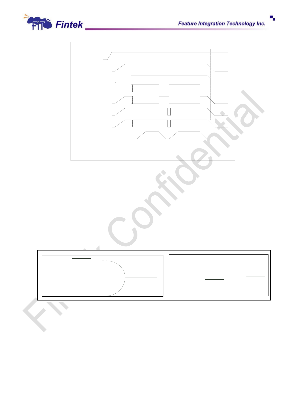
42
F71868A
VBAT
VSB
RSMRST#
S3#
PS_ON#
PSIN#
PSOUT#
3VCC
G3
S0
Figure 15 Optional timing: Always on
Delay
+3.3V
ATXPG
LRESET#
PCIRST1~5#
PWOK
Buffer
PCI Reset and PWOK Signals
The F71868A supports 5 output buffers for 5 reset signals.
So far as the PWOK issue is as the figure above. PWOK is delayed 400ms (default) as VCC
arrives 2.8V, and the delay timing can be programmed by register. An additional delay could be
added to PWOK (0ms, 100ms, 200ms and 400ms). If RSTCION# and PCIRST4#/PCIRST5# are
enabled, RSTCON# could be programmed to be asserted via PWROK or PCIRST4#/PCIRST5#.
May, 2015
V 0.17P
Page 43
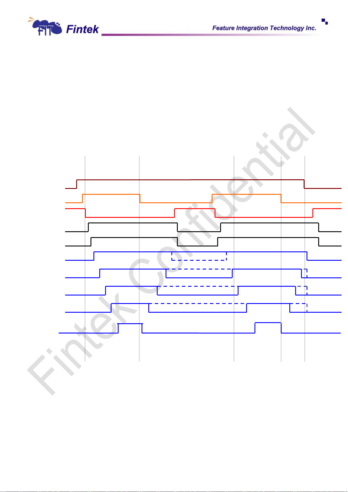
43
F71868A
5.4 AMD Power Timing Control Sequence
S5
S3
S0
S5
S5#
S3#
PSON#
ATXPWGD
TIMING_1
TIMING_2
TIMING_3
TIMING_4
CPU_PWGD
VDDOK_D400
S0
S3
The F71868A offers 4 timing pins which are designed for AMD platform power sequence
control including VDIMM, VDDA, Vcore, and VLDT (default) or other timing application purposes.
All the timings on/off are relative to S3#/S5# and can be programmed by the register 0x0AF7. As
shown in the below figure, the default timings of TIMING_1~4 are displayed in blue lines, and all
the timings are enabled in the S0 state except TIMING_1. However, TIMING_2~4 can be
programmed to enable in the S3 state, and TIMING_1 can also be programmed to disable in the
S3 state, like the dotted blue line shown in the figure below.
VDDOK_D400 is the PWOK delay timing from VDD3VOK. The default setting is that delay
400ms, there are 100ms, 200ms, and 300ms for option. It can be set in the register 0x0AF5.
Figure 16 Timing on/off sequence
The F71868A also provides AMD TSI interface for new generational CPU temperature sensing.
In AMD TSI interface, there are SIC and SID signals for temperature information reading from
AMD CPU. The SIC signal is for clocking use, the other is for data transferring. More detail, please
refer register description.
May, 2015
V 0.17P
Page 44
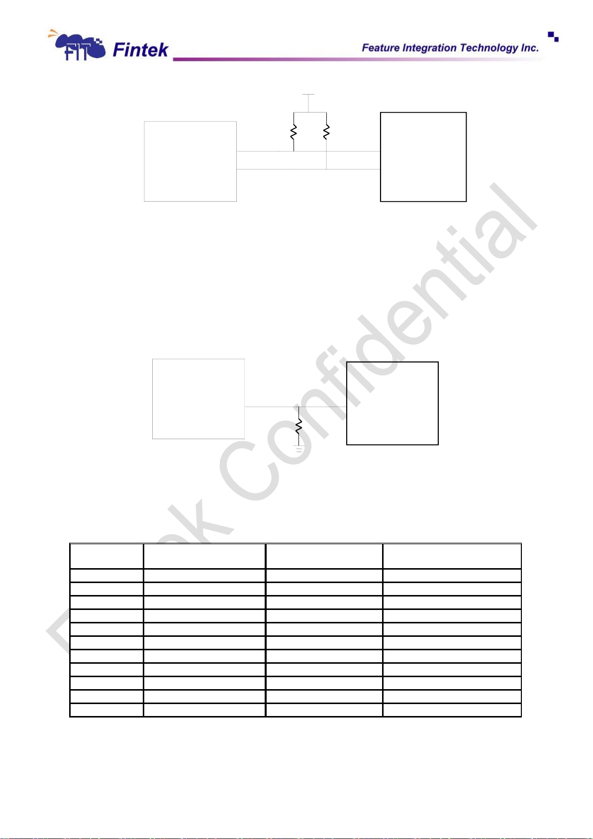
44
F71868A
SCL
VDDIO
F71868A
AMD
CPU
SIC
SID
300
300
SDA
PECI
F71868A
CPU
PECI
Intel
100K
avoid pre-BIOS floating
F71868A
Support
PECI 3.0 Command
Name
PECI 1.0 Command
Name
Status
V
Ping( )
Ping( )
V
GetTemp( )
GetTemp( )
V
GetDIB( )
V
RdIAMSR( )
-
WrIAMSR( )
-
RdPCIConfigLocal( )
Not Available in Mobile/DT
-
WrPCIConfigLocal( )
Not Available in Mobile/DT
-
RdPCIConfig( )
Not Available in Mobile/DT
-
WrPCIConfig( )
Not Available in Mobile/DT
V
RdPkgConfig( )
V
WrPkgConfig( )
Figure 17 AMD TSI typical application
5.5 Intel PECI 3.0 Functions
The F71868A provides Intel PECI/AMD TSI interfaces for new generational CPU temperature
sensing. In this interface, the F71868A can connect to CPU directly. The F71868A can read the
temperature data from CPU, than the fan control machine of F71868A can implement the Fan to
cool down CPU temperature. The application circuit is as below.
Figure 18 INTEL PECI Typical Application
In Intel PECI 3.0 Spec., it’s including below commands. The F71868A integrated most of those
commands for future advantage application. More detail, please refer the register descriptions.
May, 2015
V 0.17P
Page 45
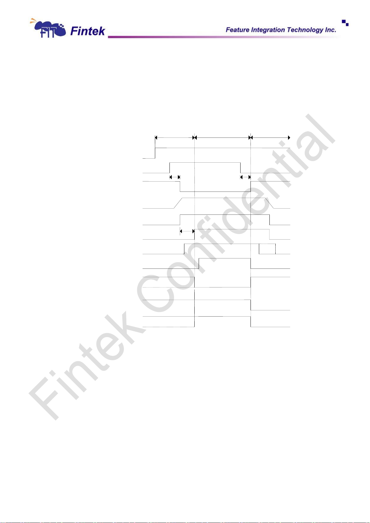
45
F71868A
S5#
S3#
PSON#
VDD3V
VDDOK
VDDOK_D400
ATXPG
PWROK
S0P5_Gate#
400ms
could be programmed low
S5
S3_Gate#
could be programmed low
S3P5_Gate#
10us
10us
S0
S3
5.6 S3_Gate#, S3P5_Gate# and S0P5_Gate# Timing
The F71868A provides three additional timing switching pins which are named as S3_Gate#,
S3P5_Gate# and S0P5_Gate#. They can be applied in the certain applications about power switch
which depends on the ACPI states. The detail timing can be referred in the following diagrams.
The default timing of S0P5_Gate# in the S5 state is low, but it can be programmed high by the
register 0x0AF6.
Figure 19 Timing chart of S5->S0->S3
May, 2015
V 0.17P
Page 46
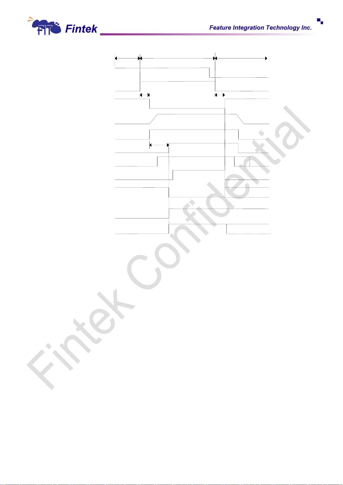
46
F71868A
S5#
S3#
PSON#
VDD3V
VDDOK
VDDOK_D400
ATXPG
PWROK
S0P5_Gate#
400ms
S3
S3_Gate#
S3P5_Gate#
10us
10us
S0
S5
could be programmed low
Figure 20 Timing chart of S3->S0->S5
5.7 Power Saving Function
5.7.1 ERP Power Saving Function
The two pins, ERP_CTRL0# and ERP_CTRL1#, which control the standby power rail on/off to
fulfill the purpose which decreases the power consumption when the system in the sleep state or
the soft-off state. These two pins connected to the external PMOSs and the defaults are high in the
sleep state in order to cut off all the standby power rails to save the power consumption. If the
system needs to support wake-up function, the two pins can be programmable to set which power
rail is turned on. The programmable register is powered by battery. So, the setting is kept even the
AC power is lost when the register is set. At the power saving state (FINTEK calls it G3-like state),
the F71868A consumes 5VSB power rail only to realize a low power consumption system. Below is
ErP function’s timing graphs.
May, 2015
V 0.17P
Page 47
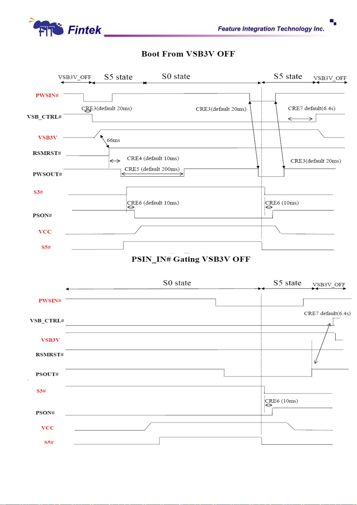
47
F71868A
May, 2015
V 0.17P
Page 48
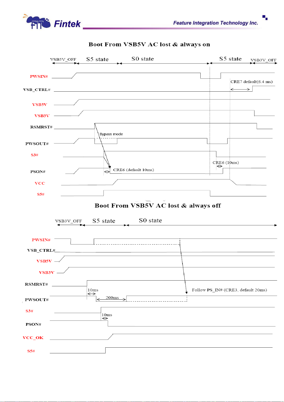
48
F71868A
May, 2015
V 0.17P
Page 49
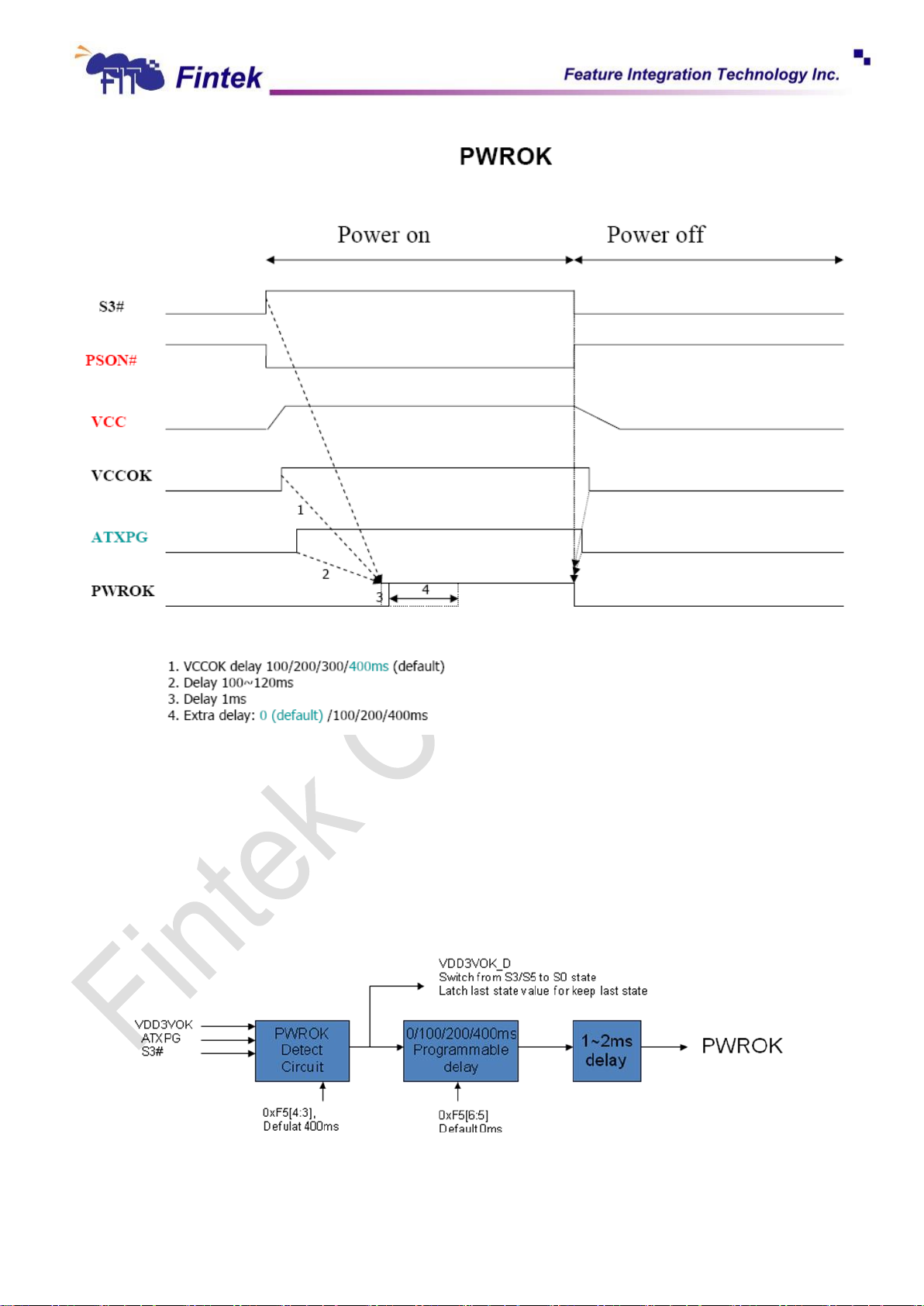
49
F71868A
5.7.2 PWROK sequence
PWROK are gated with VDD3VOK, ATXPG and S3#. PWROK is delayed 400ms (Default) when
VCC arrives 2.8V, and the delay timing can be programmed by register. An additional programmable
delay could be added to PWROK (0ms, 100ms, 200ms and 400ms).
Figure PWROK Programble Delay
May, 2015
V 0.17P
Page 50
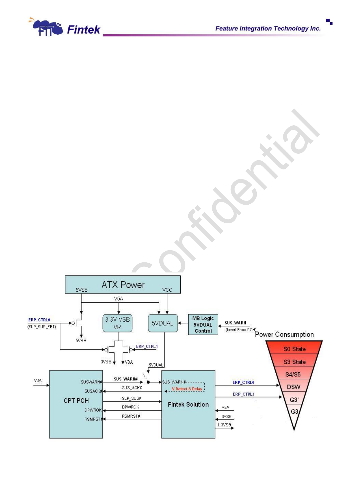
50
F71868A
5.7.3 Intel Cougar Point Timing (CPT)
The F71868A supports Intel Cougar Point Chipset timing for Sandy Bridge. There are 4 pins
for CPT control: SUS_WARN#, SUS_ACK#, SLP_SUS# and DPWROK.
For entering Intel Deep Sleep Well (DSW) state, the PCH will assert SUS_WARN# and turn off
5VDUAL. After the level of 5VDUAL is lower than 1.05V, F71868A will assert SUS_ACK# to inform
PCH it is ready for entering DSW. Finally, PCH will ramp down the internal VccSUS and assert
SLP_SUS# to F71868A. F71868A will turn off the 5VSB and 3VSB by ERP_CTRL0# and enter the
DSW state.
To exit DSW state, PCH will de-assert SLP_SUS#, turn on the SUS rail FETs and ramp up
internal 1.05V VccSUS. After the SUS rails voltages are up, RSMRST# will be desserted and the
PCH will release SUS_WARN# so that the 5VDUAL will ramp up.
Because the DSW function is controlled by F71868A instead of controlled by PCH directly,
there will be more wakeup events such as LAN, KB/Mouse, SIO RI# wake up rather than the 3
wakeup events (RTC, Power Button and GPIO27) for Intel DSW.
In order to achieve lower power consumption, F71868A provides the ERP_CTRL1# to turn off
the V3A so that the system can enter the Fintek G3’ state.
The block diagram below shows how the connection and control method for F71868A and
PCH.
May, 2015
V 0.17P
Page 51
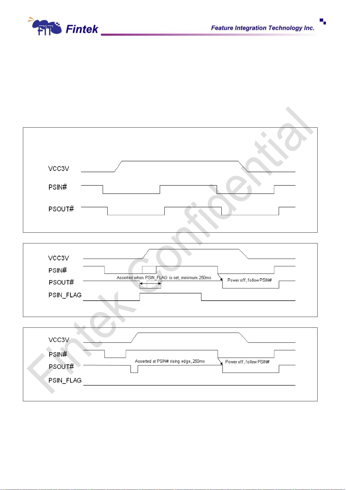
51
F71868A
When system boot from S3/S4/S5 to S0, the typical seguence is PSIN# sends pluse and then
PSOUT# sends pluse; when system off from S0 to S3/S4/S5, VCC3V will be low after PSIN# sends
pluse and then PSOUT# sends pluse.
Figure: Typical turn on Sequence
Figure: PSIN# Flag turn on detecting sequence
Figure: PSIN# Flag turn on detecting exceptional circumstance
5.8 PSIN# Detecting Flag
The purpose of PSIN# detecting flag is what detects PSIN# is pressed exceed the defined time,
and then sets a flag for BIOS usage.
The following figures below are the steps that a typical turn on sequence involves, and includes
PSIN# detecting sequence and exceptional circumstance.
May, 2015
V 0.17P
Page 52
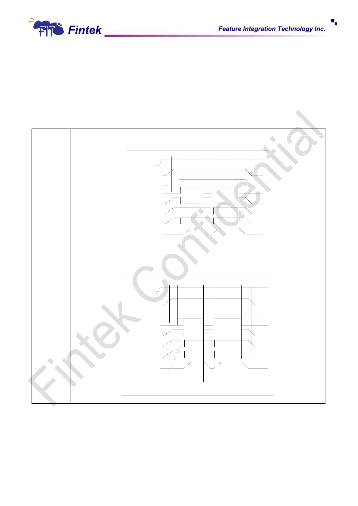
52
F71868A
5.9 AC Loss & Resume Control Methods
Mode
Explanation
Always on
(S0)
When AC resume, the system will power on automatically (send a PWSOUT# low pulse and
then sinking the PS_ON# low). See below for the timing:
VBAT
VSB
RSMRST#
S3#
PS_ON#
PSIN#
PSOUT#
VCC3V
S0S5S0S5S5
Always off
(S5)
When AC resume, the system is in off state and waiting for the wakeup events. See below for
the timing:
VBAT
VSB
RSMRST#
S3#
PS_ON#
PSIN#
PSOUT#
VCC3V
User press the button
G3S0S5S0S5
There are 5 modes under power loss state via setting ACPI control register, and they are Always On,
Always Off, Bypass Mode, Keep Last State Mode 1 and Keep Last State Mode 2.
In Keep Last State Mode 1, one register will latch the status before power loss. If it is power on before
power loss, it will automatically power on when power is resumed. If it is power off before power loss,
it will remain power off when power is resumed. See below for the detail:
May, 2015
V 0.17P
Page 53
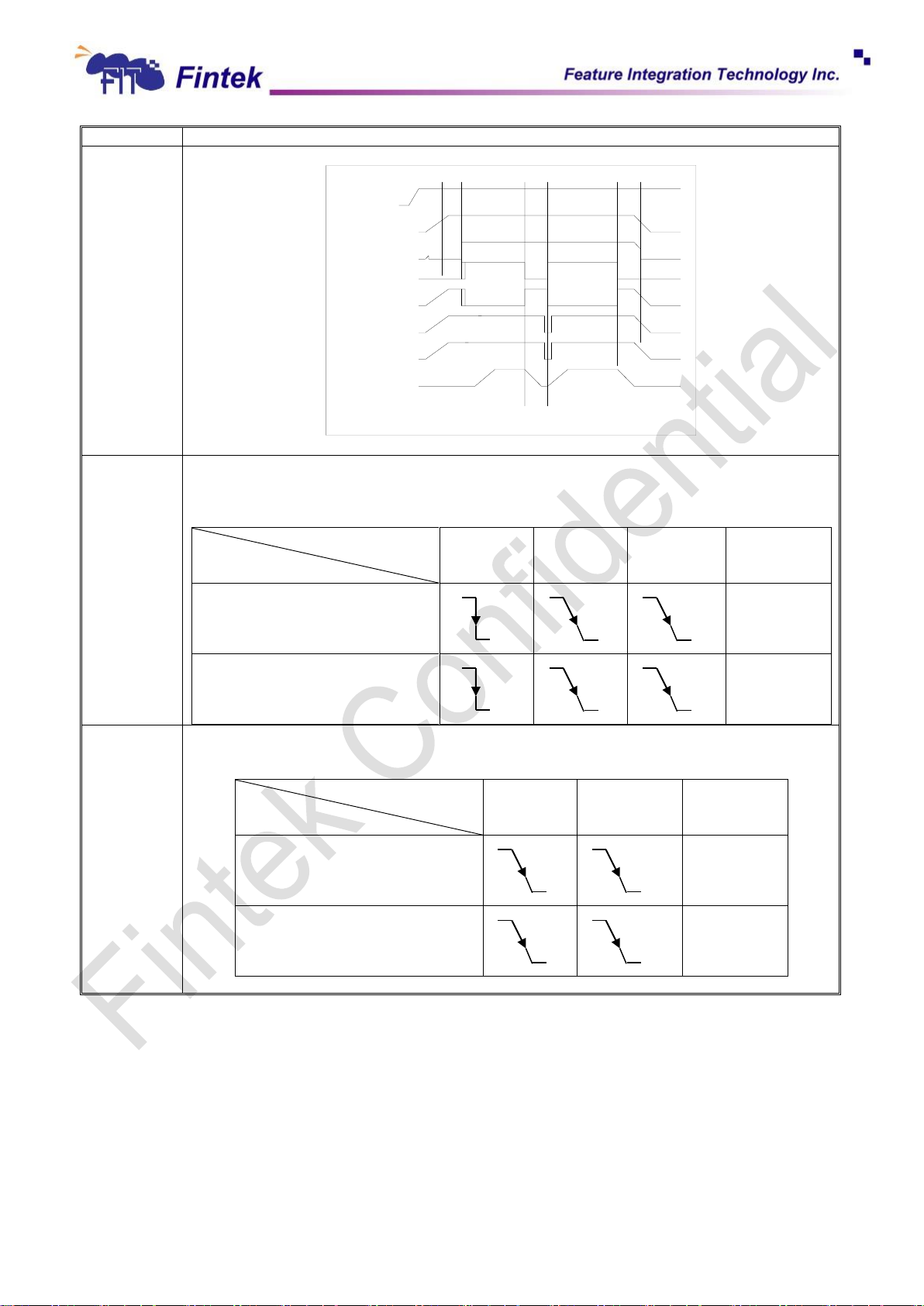
53
F71868A
Mode
Explanation
Bypass
(follow the
chipset after
G3 stage)
When AC resume, inverting the S3 signal to PS_ON#. See below for the timing:
VBAT
VSB
RSMRST#
S3#
PS_ON#
PSIN#
PSOUT#
VCC3V
S0S5S0S5S5
Keep Last
State Mode
Using ATXPG_IN, VCC (PWROK), VSB (RSMRST) and S3 signals to detect the sleep state
while AC loss occurs. One of the signal (ATXPG_IN, VCC or VSB under 2.8V) sinks low, SIO
will latch the S3 signal to decide the system to be at “always on” or “always off” mode. See
below table:
Signal
AC loss state
ATXPG
VCC
VSB
AC resume
AC loss in S0/S1 (S3=1)
Always on
AC loss in S3/S4/S5 (S3=0)
Always off
Keep Last
State Mode
New Mode
Using VCC and S3 signals to detect the sleep state while AC loss occurs.
DPWROK signal sinks low after 1~2 second, SIO will latch the S3 signal to decide the system
to be at “always on” or “always off” mode. See below table:
Signal
AC loss state
VCC
VSB
AC resume
AC loss in S0/S1 (S3=1)
Always on
AC loss in S3/S4/S5 (S3=0)
Always off
May, 2015
V 0.17P
Page 54
54
F71868A
5.10 General-Pulpose Input/Output (GPIO) Ports
PIN Name
PIN Status
Register
Reset
Pin
Power
Output
Type
Description
S0
S3
S5
GPIO0x
49 GPIO01
User Define
User Define
User Define
I_VSB3V
I_VSB3V
I/OOD
12t
50 GPIO02
User Define
User Define
User Define
I_VSB3V
I_VSB3V
I/OOD
12t
51 GPIO03
User Define
User Define
User Define
I_VSB3V
I_VSB3V
I/OOD
12t
55 GPIO04
User Define
User Define
User Define
I_VSB3V
I_VSB3V
I/OOD
12t
Multi
S3P5_Gate#/SLOTOCC#
56 GPIO05
User Define
User Define
User Define
I_VSB3V
I_VSB3V
I/OOD
12t
Multi S3_Gate#/WDTRST#
GPIO1x
59 GPIO10
User Define
User Define
User Define
I_VSB3V
I_VSB3V
I/OOD
12st5v
Multi PCIRST4#/SCL
60 GPIO11
User Define
User Define
User Define
I_VSB3V
I_VSB3V
I/OOD
12st5v
Multi PCIRST5#/SDA
61 GPIO12
User Define
User Define
User Define
I_VSB3V
I_VSB3V
I/OOD
12st5v
Multi RSTCON#
62 GPIO13
User Define
User Define
User Define
I_VSB3V
I_VSB3V
I/OOD
20st5v
Multi S0P5_Gate#
63 GPIO14
User Define
User Define
User Define
I_VSB3V
I_VSB3V
I/OOD
12st5v
Multi WDTRST#
64 GPIO15
User Define
User Define
User Define
I_VSB3V
I_VSB3V
I/OOD
12st5v
Multi LED_VSB/ALERT#
65 GPIO16
User Define
User Define
User Define
I_VSB3V
I_VSB3V
I/OOD
12st5v
Multi LED_VCC
66 GPIO17
User Define
User Define
User Define
I_VSB3V
I_VSB3V
I/OOD
12st5v
Multi CPU_PWGD
GPIO2x
126 GPIO20
User Define
Z
Z
LRESET#
3VCC
I/OOD
12st5v
Multi DCD2#/SEGG
127 GPIO21
User Define
Z
Z
LRESET#
3VCC
I/OOD
12st5v
Multi RI2#/SEGF
128 GPIO22
User Define
Z
Z
LRESET#
3VCC
I/OOD
12st5v
Multi CTS2#/SEGA
1 GPIO23
User Define
Z
Z
LRESET#
3VCC
I/OOD
12st5v
Multi DTR2#/SEGD
2 GPIO24
User Define
Z
Z
LRESET#
3VCC
I/OOD
12st5v
Multi RTS2#/SEGC
3 GPIO25
User Define
Z
Z
LRESET#
3VCC
I/OOD
12st5v
Multi DSR2#/L#
5 GPIO26
User Define
Z
Z
LRESET#
3VCC
I/OOD
12st5v
6GPIO27
User Define
Z
Z
LRESET#
3VCC
I/OOD
12st5v
Multi SIN2#/SEGE
GPIO3x
7 GPIO30
User Define
Z
Z
I_VSB3V
3VCC
I/OD
14st5v
8 GPIO31
User Define
Z
Z
I_VSB3V
3VCC
I/OD
14st5v
9 GPIO32
User Define
Z
Z
I_VSB3V
3VCC
I/OD
14st5v
Each pin is configured independently as input or I/O (all GPIOs without static pull-up and without pull-down) and with
either open-drain or push-pull output type.
Table: F71868A GPIO Table
May, 2015
V 0.17P
Page 55
55
F71868A
PIN Name
PIN Status
Register
Pin
Output
Description
10 GPIO33
User Define
Z
Z
I_VSB3V
3VCC
I/OD
14st5v
11 GPIO34
User Define
Z
Z
I_VSB3V
3VCC
I/OD
14st5v
12 GPIO35
User Define
Z
Z
I_VSB3V
3VCC
I/OD
14st5v
13 GPIO36
User Define
Z
Z
I_VSB3V
3VCC
I/OD
14st5v
14 GPIO37
User Define
Z
Z
I_VSB3V
3VCC
I/OD
14st5v
GPIO4x
25 GPIO40
User Define
Z
Z
I_VSB3V
3VCC
I/OOD
12st5v
Multi FANIN3
26 GPIO41
User Define
Z
Z
I_VSB3V
3VCC
I/OOD
12st5v
Multi FANCTL3
27 GPIO42
User Define
Z
Z
I_VSB3V
3VCC
I/OOD
12st5v
Multi IRTX
28 GPIO43
User Define
Z
Z
I_VSB3V
3VCC
I/OOD
12st5v
Multi IRRX
78 GPIO44
User Define
User Define
User Define
I_VSB3V
I_VSB3V
I/OOD
12st5v
Multi ATXPG_IN
80 GPIO45
User Define
User Define
User Define
I_VSB3V
I_VSB3V
I/OOD
12st5v
Multi PSIN#
81 GPIO46
User Define
User Define
User Define
I_VSB3V
I_VSB3V
I/OOD
12st5v
Multi PSOUT#
83 GPIO47
User Define
User Define
User Define
I_VSB3V
I_VSB3V
I/OD
12st5v
Multi S3#
GPIO5x
15 GPIO50
User Define
Z
Z
I_VSB3V
3VCC
I/OD
12st5v
16 GPIO51
User Define
Z
Z
I_VSB3V
3VCC
I/OD
12st5v
17 GPIO52
User Define
Z
Z
I_VSB3V
3VCC
I/OD
12st5v
18 GPIO53
User Define
Z
Z
I_VSB3V
3VCC
I/OD
12st5v
19 GPIO54
User Define
Z
Z
I_VSB3V
3VCC
I/OD
12st5v
GPIO6x
User Define
Z
Z
LRESET#
3VCC
I/OOD
12st5v
Multi SLCT
User Define
Z
Z
LRESET#
3VCC
I/OOD
12st5v
Multi PE
User Define
Z
Z
LRESET#
3VCC
I/OOD
12st5v
Multi BUSY
User Define
Z
Z
LRESET#
3VCC
I/OOD
12st5v
Multi ACK#
User Define
Z
Z
LRESET#
3VCC
I/OOD
12st5v
Multi INT#
User Define
Z
Z
LRESET#
3VCC
I/OOD
12st5v
Multi ERR#
User Define
Z
Z
LRESET#
3VCC
I/OOD
12st5v
Multi AFD#
User Define
Z
Z
LRESET#
3VCC
I/OOD
12st5v
Multi STB#
GPIO7x
User Define
Z
Z
LRESET#
3VCC
I/OOD
12st5v
Multi PD0
User Define
Z
Z
LRESET#
3VCC
I/OOD
12st5v
Multi PD1
User Define
Z
Z
LRESET#
3VCC
I/OOD
12st5v
Multi PD2
User Define
Z
Z
LRESET#
3VCC
I/OOD
12st5v
Multi PD3
User Define
Z
Z
LRESET#
3VCC
I/OOD
12st5v
Multi PD4
User Define
Z
Z
LRESET#
3VCC
I/OOD
12st5v
Multi PD5
May, 2015
V 0.17P
Page 56

56
F71868A
PIN Name
PIN Status
Register
Pin
Output
Description
User Define
Z
Z
LRESET#
3VCC
I/OOD
12st5v
Multi PD6
User Define
Z
Z
LRESET#
3VCC
I/OOD
12st5v
Multi PD7
May, 2015
V 0.17P
Page 57

57
F71868A
6. Register Description
Global Control Registers
Register
0x[HEX]
Register Name
Default Value
MSB LSB
02
Software Reset Register
- - - - - - - 0 07
Logic Device Number Register (LDN)
0 0 0 0 0 0 0 0 20
Chip ID Register 1
0 0 0 1 0 0 0 1 21
Chip ID Register 2
0 0 0 0 0 1 1 0 23
Vendor ID Register 1
0 0 0 1 1 0 0
1
24
Vendor ID Register 2
0 0 1 1 0 1 0
0
The configuration register is used to control the behavior of the corresponding devices. To
configure the register, using the index port to select the index and then writing data port to alter the
parameters. The default index port and data port are 0x4E and 0x4F respectively. Pull down the
SOUT1 pin to change the default value to 0x2E/0x2F. To enable configuration, the entry key 0x87
must be written to the index port. To disable configuration, write exit key 0xAA to the index port.
Following is a example to enable configuration and disable configuration by using debug.
-o 4e 87
-o 4e 87 (enable configuration)
-o 4e aa (disable configuration)
The Following is a register map (total devices) grouped in hexadecimal address order, which shows
a summary of all registers and their default value. Please refer each device chapter if you want
more detail information.
Global Control Registers
“-“ Reserved or Tri-State
May, 2015
V 0.17P
Page 58
58
F71868A
25
Software Power Down Register
- - - - 0 0 0 0 26
UART IRQ Sharing Register
0 - 0 - 0 0 0 0 27
Configuration Port Select Register
1/0 0 1/0
1/0 - - - 1/0
28
Multi-function Select Register1
0 0 1 1 1 0 0 0 29
Multi-function Select Register2
0 1 1 0 1 1 1 1 29
WDT Clock Divisor High Byte
- - - - 0 0 1 1 2A
Multi-function Select Register3
0 0 0 0 1 1 1 1 2A
WDT Clock Divisor Low Byte
1 1 1 0 0 1 1 1 2B
Multi-function Select Register4
0 0 0 0 1 1 1 1 2B
WDT Clock Fine Tune Count High Byte
- - - - - - - - 2C
Multi-function Select Register 5
0 0 0 0 0 0 0 0 2C
WDT Clock Fine Tune Count Low Byte
- - - - - - - - 2D
Wakeup Control Register
0 0 1 0 1 0 0
0
UART1 Device Configuration Registers (LDN CR01)
Register
0x[HEX]
Register Name
Default Value
MSB LSB
30
UART1 Device Enable Register
- - - - - - - 1 60
Base Address High Register
0 0 0 0 0 0 1 1 61
Base Address Low Register
1 1 1 1 1 0 0 0 70
IRQ Channel Select Register
- - - - 0 1 0 0 F0
RS485 Enable Register
- - 0 0 - - -
-
UART2 Device Configuration Registers (LDN CR02)
Register
0x[HEX]
Register Name
Default Value
MSB LSB
30
UART2 Device Enable Register
- - - - - - - 1 60
Base Address High Register
0 0 0 0 0 0 1
0
61
Base Address Low Register
1 1 1 1 1 0 0
0
70
IRQ Channel Select Register
- - - - 0 0 1 1 F0
RS485 Enable Register
- - - 0 0 0 - - F1
SIR Mode Control Register
- - 0 0 0 1 0
0
Parallel Port Device Configuration Registers (LDN CR03)
Register
0x[HEX]
Register Name
Default Value
MSB LSB
Device Configuration Registers
“-“ Reserved or Tri-State
May, 2015
V 0.17P
Page 59
59
F71868A
30
Parallel Port Device Enable Register
- - - - - - - 1 60
Base Address High Register
0 0 0 0 0 0 1 1 61
Base Address Low Register
0 1 1 1 1 0 0 0 70
IRQ Channel Select Register
- - - - 0 1 1 1 74
DMA Channel Select Register
- - - 0 - 0 1 1 F0
PRT Mode Select Register
0 1 0 0 0 0 1
0
Hardware Monitor Device Configuration Registers (LDN CR04)
Register
0x[HEX]
Register Name
Default Value
MSB LSB
30
H/W Monitor Device Enable Register
- - - - - - - 1 60
Base Address High Register
0 0 0 0 0 0 1
0
61
Base Address Low Register
1 0 0 1 0 1 0 1 70
IRQ Channel Select Register
- - - - 0 0 0
0
KBC Device Configuration Registers (LDN CR05)
Register
0x[HEX]
Register Name
Default Value
MSB LSB
30
KBC Device Enable Register
- - - - - - - 1 60
Base Address High Register
0 0 0 0 0 0 0 0 61
Base Address Low Register
0 1 1 0 0 0 0 0 70
KB IRQ Channel Select Register
- - - - 0 0 0 1 72
Mouse IRQ Channel Select Register
- - - - 1 1 0 0 F0
Clock Select Register
1 0 - - - - 1 1 FE
Swap Register
1 - - 0 0 0 0 1 FF
User Wakeup Code Register
0 0 1 0 1 0 0
1
GPIO Device Configuration Registers (LDN CR06)
Register
0x[HEX]
Register Name
Default Value
MSB LSB
30
GPIO Device Enable Register
- - - - - - - 0 60
Base Address High Register
0 0 0 0 0 0 0 0 61
Base Address Low Register
0 0 0 0 0 0 0
0
70
GPIRQ Channel Select Register
- - - - 0 0 0 0 F0
GPIO Output Enable Register
- - 0 0 0 0 0 0 F1
GPIO Output Data Register
- - 1 1 1 1 1 1 F2
GPIO Pin Status Register
- - - - - - - - F3
GPIO Drive Enable Register
- - 0 0 0 0 0
0
E0
GPIO1 Output Enable Register
0 0 0 0 0 0 0 0 E1
GPIO1 Output Data Register
1 1 1 1 1 1 1
1
May, 2015
V 0.17P
Page 60
60
F71868A
E2
GPIO1 Pin Status Register
- - - - - - - - E3
GPIO1 Drive Enable Register
0 0 0 0 0 0 0 0 E4
GPIO1 PME Enable Register
0 0 0 0 0 0 0 0 E5
GPIO1 Detect Edge Select Register
0 0 0 0 0 0 0 0 E6
GPIO1 PME Status Register
0 0 0 0 0 0 0 0 D0
GPIO2 Output Enable Register
0 0 0 0 0 0 0 0 D1
GPIO2 Output Data Register
1 1 1 1 1 1 1 1 D2
GPIO2 Pin Status Register
- - - - - - - - D3
GPIO2 Drive Enable Register
0 0 0 0 0 0 0 0 C0
GPIO3 Output Enable Register
0 0 0 0 0 0 0 0 C1
GPIO3 Output Data Register
1 1 1 1 1 1 1 1 C2
GPIO3 Pin Status Register
- - - - - - - - B0
GPIO4 Output Enable Register
- - - - 0 0 0 0 B1
GPIO4 Output Data Register
- - - - 1 1 1 1 B2
GPIO4 Pin Status Register
- - - - - - - - B3
GPIO4 Drive Enable Register
- - - - 0 0 0 0 B4
GPIO4 PME Enable Register
- - - - 0 0 0 0 B5
GPIO4 Detect Edge Select Register
- - - - 0 0 0 0 B6
GPIO4 PME Status Register
- - - - 0 0 0 0 A0
GPIO5 Output Enable Register
- - - 0 0 0 0 0 A1
GPIO5 Output Data Register
- - - 1 1 1 1 1 A2
GPIO5 Pin Status Register
- - - - - - - - A4
GPIO5 PME Enable Register
0 0 0 0 0 0 0 0 A5
GPIO5 Detect Edge Select Register
0 0 0 0 0 0 0 0 A6
GPIO5 PME Status Register
0 0 0 0 0 0 0 0 90
GPIO6 Output Enable Register
0 0 0 0 0 0 0 0 91
GPIO6 Output Data Register
1 1 1 1 1 1 1 1 92
GPIO6 Pin Status Register
- - - - - - - - 80
GPIO7 Output Enable Register
0 0 0 0 0 0 0 0 81
GPIO7 Output Data Register
1 1 1 1 1 1 1
1
82
GPIO7 Pin Status Register
- - - - - - -
-
83
GPIO7 Drive Enable Register
0 0 0 0 0 0 0
0
WDT Device Configuration Registers (LDN CR07)
Register
0x[HEX]
Register Name
Default Value
MSB LSB
F0
Watchdog Timer Enable Register
- - - - - - - 1 F2
BUS Manual Register
0 0 0 0 0 0 0
0
May, 2015
V 0.17P
Page 61
61
F71868A
F3
Key Data Register
0 0 0 0 0 0 0 0 F4
BUSIN Status Register
- - - - - - - - F5
WDT Unit Select Register
- 0 - 0 0 0 0 0 F6
WDT Count Register
0 0 0 0 1 0 1 0 F7
Watchdog Timer PME Register
0 0 0 - - - -
0
PME, ACPI, and ERP Power Saving Device Configuration Registers (LDN CR0A)
Register
0x[HEX]
Register Name
Default Value
MSB LSB
30
PME Device Enable Register
- - - - - - - 0 E0
ERP Enable Register
0 - - - - - 0 0 E1
ERP Control Register
1 1 0 0 1 1 0
0
E2
ERP Control Register
- 0 1 1 1 1 0 - E3
ERP PSIN Deb-Register
0 0 0 1 0 0 1
1
E4
ERP RSMRST Deb-Register
0 0 0 0 1 0 0 1 E5
ERP PSOUT Deb-Register
1 1 0 0 0 1 1 1 E6
ERP PSON Deb-Register
0 0 0 0 1 0 0 1 E7
ERP S5 Delay Register
0 1 1 0 0 0 1 1 E8
Wakeup Enable Register
0 - 0 0 1 0 0 0 E9
ERP S3 Delay Register
0 0 0 0 1 1 1 1 EC
ERP Mode Select Register
0 0 0 - - - - - ED
ERP WDT Control Register
- - - - - - 0 0 EE
ERP WDT Timer
- - - - - - - 0 F0
PME Event Enable Register 1
0 0 0 0 0 0 0 0 F1
PME Event Status Register 1
- - - - - - - - F2
PME Event Enable Register 2
- - - 0 - 0 0 0 F3
PME Event Status Register 2
- - - - - - - - F4
Keep Last State Select Register
0 0 0 0 0 1 1 0 F5
VDDOK Delay Select Register
0 0 0 1 1 1 0 0 F6
PCIRST Control Register
0 0 0 1 1 1 1 1 F7
Power Sequence Control Register
1 0 0 0 0 1 1
0
F8
LED VCC Control Register
0 0 0 0 0 0 0
0
F9
LED VSB Control Register
- 0 0 0 0 0 0 0 FA
LED VSB Additional Control Register
- 0 0 0 - 0 0
0
FB
PWROK Gate Enable Register and PSIN#
Detect Register
0 0 0 0 - 0 0
0
FC
Intel DSW Delay Register
- - - - 0 1 1 1 FE
RI De-bounce Select Register
0 0 - 0 - - 0
0
May, 2015
V 0.17P
Page 62
62
F71868A
6.1 Global Control Registers
Bit
Name
R/W
Default
Description
7-1
Reserved
- - Reserved
0
SOFT_RST
R/W
0
Write 1 to reset the register and device powered by VDD ( 3VCC ).
Bit
Name
R/W
Default
Description
7-0
LDN
R/W
00h
00h: Reserved
01h: Select UART 1 device configuration registers.
02h: Select UART 2 device configuration registers.
03h: Select Parallel Port device configuration registers.
04h: Select Hardware Monitor device configuration registers.
05h: Select KBC device configuration registers.
06h: Select GPIO device configuration registers.
07h: Select WDT device configuration registers.
0ah: Select PME & ACPI device configuration registers.
Bit
Name
R/W
Default
Description
7-0
Chip_ID1
R
11h
Chip ID1
Bit
Name
R/W
Default
Description
7-0
Chip_ID2
R
06h
Chip ID2
Bit
Name
R/W
Default
Description
7-0
Vendor_ID1
R
19h
Vendor ID1
6.1.1 Software Reset Register Index 02h
6.1.2 Logic Device Number Register (LDN) Index 07h
6.1.3 Chip ID Register 1 Index 20h
6.1.4 Chip ID Register 2 Index 21h
6.1.5 Vendor ID Register 1 Index 23h
May, 2015
V 0.17P
Page 63
63
F71868A
6.1.6 Vendor ID Register 2 Index 24h
Bit
Name
R/W
Default
Description
7-0
Vendor_ID2
R
34h
Vendor ID2
Bit
Name
R/W
Default
Description
7-4
Reserved
-
-
Reserved.
3
SOFTPD_PRT
R/W
0
Set “1” to power down Parallel Port. The clock will stop.
2
SOFTPD_UR2
R/W
0
Set “1” to power down UART 2. The clock will stop.
1
SOFTPD_UR1
R/W
0
Set “1” to power down UART 1. The clock will stop.
0
Reserved
- - Reserved.
Bit
Name
R/W
Default
Description
7
CLK24M_SEL
R/W
0
0: CLKIN is 48MHz
1: CLKIN is 24MHz
6
Reserved
- - Reserved.
5
DPORT_DEC_SEL
R/W
0
0: The debug port address is 0x80.
1: The debug port address is UART2 base address.
4
Reserved
-
-
Reserved.
3
CLK_TUNE_EN
R/W
0
Set “1” to switch index 0x29 ~ 0x2C to WDT clock fine tune registers.
2
TX_DEL_1BIT
R/W
0
0: UART transmits data immediately after writing THR.
1: UART transmits data delay one bit time after writing THR.
1
IRQ_MODE
R/W
0
0: PCI IRQ sharing mode (low level).
1: ISA IRQ sharing mode (low pulse).
0
IRQ_SHAR
R/W
0
0: disable IRQ sharing of two UART devices.
1: enable IRQ sharing of two UART devices.
Bit
Name
R/W
Default
Description
6.1.7 Software Power Down Register Index 25h
6.1.8 UART IRQ Sharing Register Index 26h
6.1.9 Configuration Port Select Register Index 27h
May, 2015
V 0.17P
Page 64
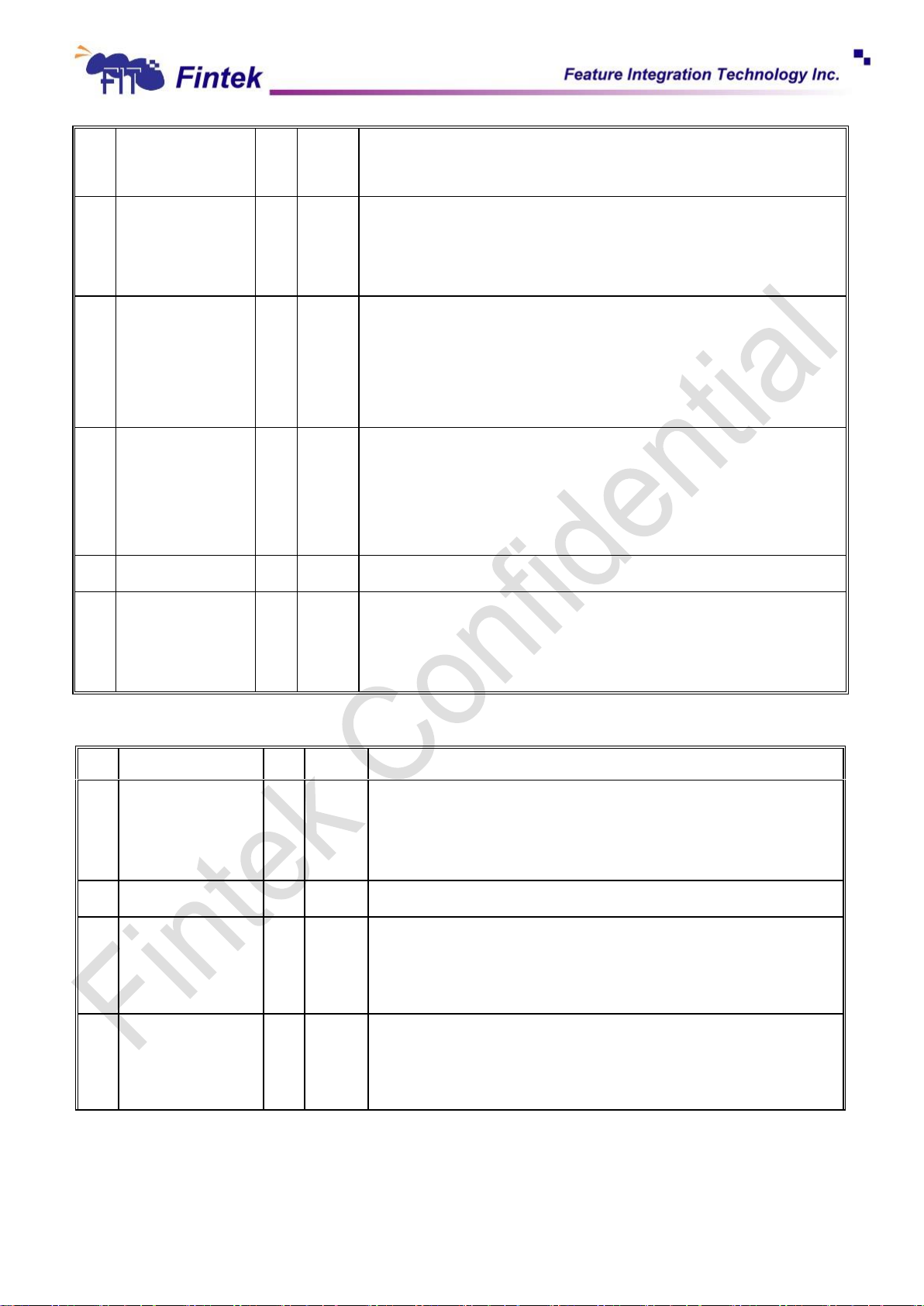
64
F71868A
7
OVP_MODE
R/W
1
1: Alarm mode.
0: Force mode.
6
TEMP_OUT_EN
R/W
0
Debug port output select.
0: 80 port data.
1: Temperature fetched by hardware mmonitor.
5
DPORT_EN
R/W
-
0: Disable debug port.
1: Enable debug port.
This bit is power on strapped by
GPIO26/SOUT2/SEGB/STRAP_DPORT. Pull down to disable.
4
PORT_4E_EN
R/W
-
0: The configuration register port is 2E/2F.
1: The configuration register port is 4E/4F.
This register is power on trapped by SOUT1/ Config4E_2E. Pull down
to select port 2E/2F.
3-1
Reserved
- - Reserved.
0
TIMING_EN
R
-
This bit is the pin status of TIMING_GPIO pin.
0: Disable power sequence control.
1: Enable power sequence control.
Bit
Name
R/W
Default
Description
7
GP_RST_SEL
R/W
0
Select GPIO5/GPIO3 reset signal.
0: Reset by internal VSB3V power good.
1: Reset by LRESET#.
6
Reserved
R/W
0
Reserved
5
PWR_
S3_Gate#_EN
R/W
1
0: S3_Gate#/GPIO05/WDTRST# functions as GPIO05/WDTRST#
determined by GPIO05_EN.
1: S3_Gate#/GPIO05/WDTRST# functions as S3_Gate#.
4
PWR_
S3P5_Gate#_EN
R/W
1
0: S3P5_Gate#/SLOTOCC#/GPIO04 functions as
SLOTOCC#/GPIO04 determined by GPIO04_EN.
1: S3P5_Gate#/SLOTOCC#/GPIO04 functions as S3P5_Gate#.
6.1.10 Multi-Function Select Register 1 Index 28h (Powered by VSB3V)
May, 2015
V 0.17P
Page 65
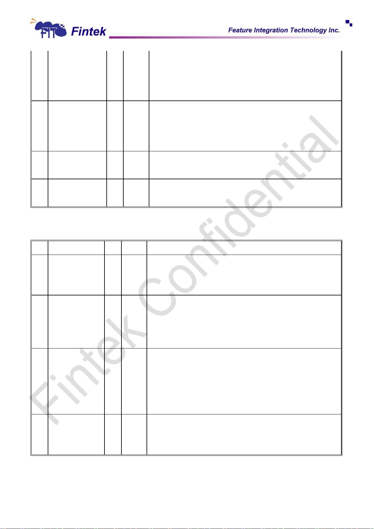
65
F71868A
3
GPIO05_EN
R/W
1
0: S3_Gate#/GPIO05/WDTRST# functions as WDTRST if PWR_
S3_Gate#_EN is not set.
1: S3_Gate#/GPIO05/WDTRST# functions as GPIO05 is PWR_
S3_Gate#_EN is not set.
2
GPIO04_EN
R/W
0
0: S3P5_Gate#/SLOTOCC#/GPIO04 functions as SLOTOCC# if
PWR_ S3P5_Gate#_EN is not set.
1: S3P5_Gate#/SLOTOCC#/GPIO04 functions as GPIO04 if PWR_
S3P5_Gate#_EN is not set.
1
PIN60_LVL_SEL
R/W
0
0: Pin 60 input level is TTL level.
1: Pin 60 input level is low level (0.6V/0.9V).
0
PIN59_LVL_SEL
R/W
0
0: Pin 59 input level is TTL level.
1: Pin 59 input level is low level (0.6V/0.9V).
Bit
Name
R/W
Default
Description
7
GPIO17_EN
R/W
0
CPU_PWGD/GPIO17 function select.
0: The pin function is CPU_PWGD.
1: The pin function is GPIO17.
6
GPIO16_EN*
R/W
1
GPIO16/LED_VCC function select.
0: The pin function is LED_VCC.
1: The pin function is GPIO16.
This bit is powered by VBAT.
5
GPIO15_EN
R/W
1
GPIO15/LED_VSB/ALERT# function select.
{LED_VSB_EN, GPIO15_EN}
1x: The pin function is LED_VSB.
01: The pin function is GPIO15.
00: The pin function is ALERT#.
4
GPIO14_EN
R/W
0
WDTRST#/GPIO14 function select.
0: The pin function is WDTRST#.
1: The pin function is GPIO14.
6.1.11 Multi-Function Select Register 2 Index 29h (Powered by VBAT CLK_TUNE_EN = 0)
May, 2015
V 0.17P
Page 66
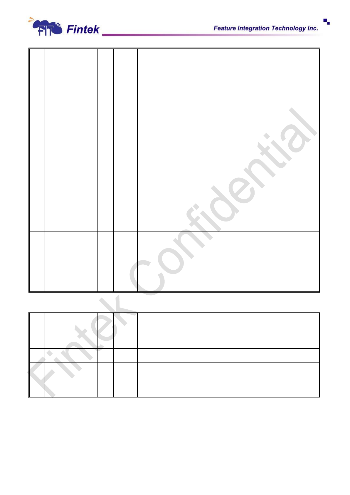
66
F71868A
3
GPIO13_EN
R/W
1
S0P5_Gate#/GPIO13/BEEP function select.
If S0P5_Gate#_EN is set , the pin function is S0P5_Gate#, The pin
function is determined by
{ S0P5_Gate#_EN, GPIO13_EN}
1x: The pin function is S0P5_Gate#.
01: The pin function is GPIO13.
00: The pin function is BEEP.
2
GPIO12_EN
R/W
1
GPIO12/ RSTCON#/FANCTL1 function select.
0: The pin function is FANCTL1.
1: The pin function is GPIO12.
1
GPIO11_EN
R/W
1
GPIO11/PCIRST5#/SDA function select.
If IBX_ALT_EN is set , the pin function is SDA, otherwise the pin
function is determined by this bit:
0: The pin function is PCIRST5#.
1: The pin function is GPIO11.
0
GPIO10_EN
R/W
1
GPIO10/PCIRST4#/SCL function select.
If IBX_ALT_EN is set , the pin function is SCL, otherwise the pin
function is determined by this bit:
0: The pin function is PCIRST4#.
1: The pin function is GPIO10.
Bit
Name
R/W
Default
Description
7
WDT_TUNE_STAR
T
W
-
Write “1” to this bit to start count internal 500KHz period (10 times).
6-4
Reserved
-
-
Reserved.
3-0
WDT_CLK_DIV[11:
8]
R/W
3h
This is the high nibble of 12-bit divisor for WDT clock. The clock used
for WDT is 10Hz which is divided by internal 10KHz clock. Program
this divisor to fine tune clock.
6.1.12 WDT Clock Divisor High Byte Index 29h (Powered by VBAT, CLK_TUNE_EN = 1)
May, 2015
V 0.17P
Page 67
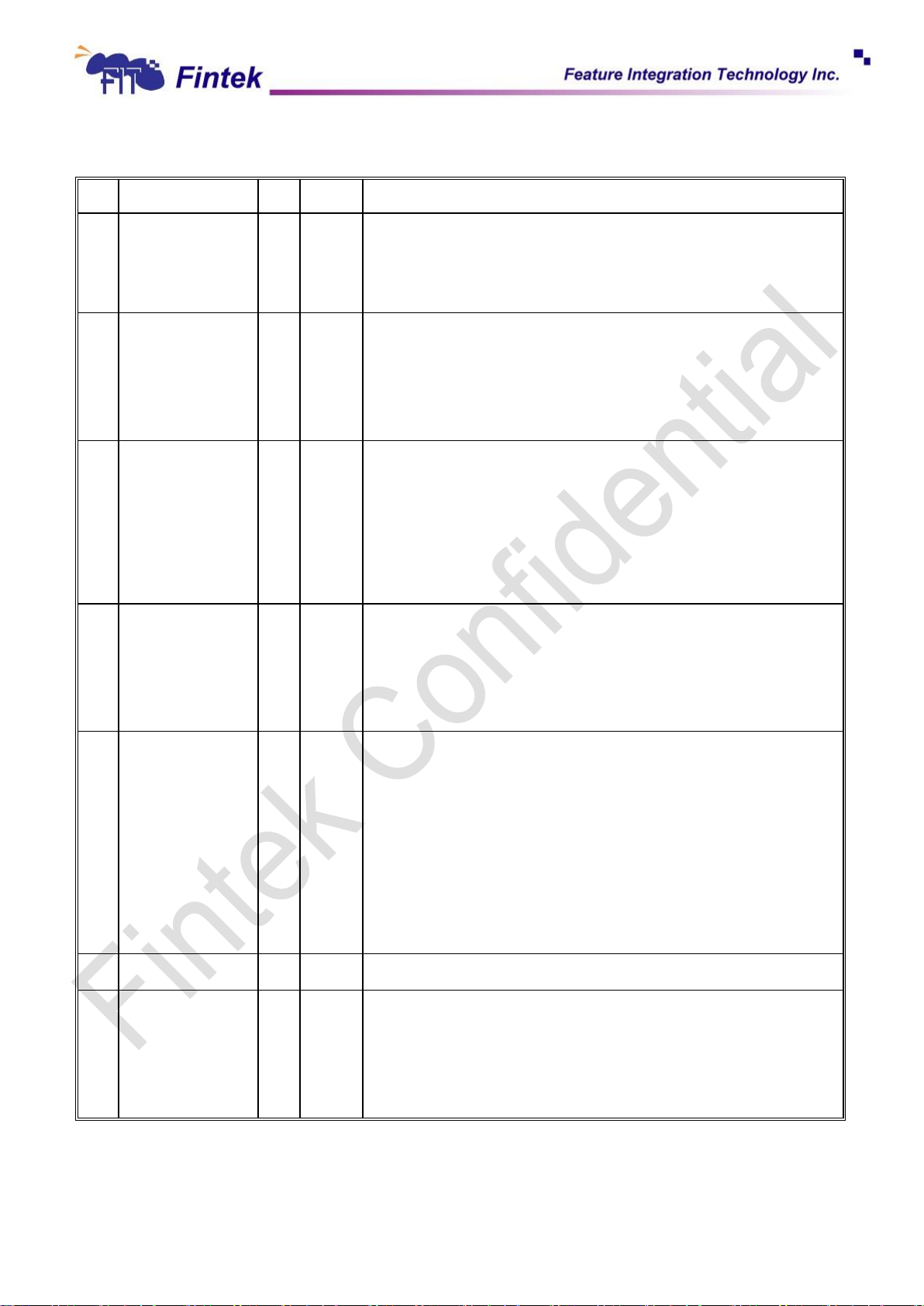
67
F71868A
6.1.13 Multi-Function Select Register 3 Index 2Ah (Powered by VBAT, CLK_TUNE_EN = 0)
Bit
Name
R/W
Default
Description
7
LPT_GP_EN
R/W
0
Parallel Port/GPIO function select.
0: Pin 100 ~ 116 functions as Parallel Port.
1: Pin 100 ~ 116 functions as GPIO6 and GPIO7.
6
IBX_ALT_EN
R/W
0
Alternative IBX pin enable.
0: Disable IBX alternative pins.
1: Enable IBS alternative pins. See GPIO11_EN and GPIO10_EN for
detail.
5
LED_VSB_EN
R/W
0
GPIO15/LED_VSB/ALERT# function select.
{LED_VSB_EN, GPIO15_EN}
1x: The pin function is LED_VSB.
01: The pin function is GPIO15.
00: The pin function is ALERT#.
4
RSTCON_PIN_EN
R/W
0
RSTCON# Enable Register:
0: The pin function of GPIO12/ RSTCON#/FANCTL1 is GPIO12/
FANCTL1
1: The pin function of GPIO12/RSTCON#/FANCTL1 is RSTCON#.
3
S0P5_Gate# _EN
R/W
1
S0P5_Gate#/GPIO13/BEEP function select.
If S0P5_Gate#_EN is set , the pin function is S0P5_Gate#, The pin
function is determined by
{ S0P5_Gate#_EN, GPIO13_EN}
1x: The pin function is S0P5_Gate#.
01: The pin function is GPIO13.
00: The pin function is BEEP.
2
Reserved
R/W
1
Reserved
1
UR2_GP_EN2
R/W
1
= 0 set pin5, 6 to be SOUT2 and SIN2
= 1 will change pin5, 6 (SOUT2 and SIN2) to GPIOs.
Set UR2_GP_EN1 and UR2_GP_EN2 will also disable UART2 I/O
port.
May, 2015
V 0.17P
Page 68
68
F71868A
0
UR2_GP_EN1
R/W
1
= 0 will change pin 1, 2, 3, 126, 127 and 128 to be DTR2#, RTS2#,
DSR2#, DCD2#, RI2# and CTS2#.
= 1 will change pin 1, 2, 3, 126, 127 and 128 to be GPIO.
Set UR2_GP_EN1 and UR2_GP_EN2 will also disable UART2 I/O
port.
Bit
Name
R/W
Default
Description
7-0
WDT_CLK_DIV[7:0]
R/W
E7h
This is the high nibble of 12-bit divisor for WDT clock. The clock used
for WDT is 10Hz which is divided by internal 10KHz clock. Program
this divisor to fine tune clock.
Bit
Name
R/W
Default
Description
7
GPIO47_EN
R/W
0
PSON#/GPIO47 function select.
0: The pin function is PSON#.
1: The pin function is GPIO47.
6
GPIO46_EN
R/W
0
PSOUT#/GPIO46 function select.
0: The pin function is PSOUT#.
1: The pin function is GPIO46.
5
GPIO45_EN
R/W
0
PSIN#/GPIO45 function select.
0: The pin function is PSIN#.
1: The pin function is GPIO45.
4
GPIO44_EN
R/W
0
ATXPG_IN/GPIO44 function select.
0: The pin function is ATXPG_IN.
1: The pin function is GPIO44.
3
GPIO43_EN
R/W
1
GPIO43/IRRX function select.
0: The pin function is IRRX.
1: The pin function is GPIO43.
2
GPIO42_EN
R/W
1
GPIO42/IRTX function select.
0: The pin function is IRTX.
1: The pin function is GPIO42.
6.1.14 WDT Clock Divisor Low Byte Index 2Ah (Powered by VBAT, CLK_TUNE_EN = 1)
6.1.15 Multi-Function Select Register 4 Index 2Bh (Powered by VSB3V, CLK_TUNE_EN = 0)
May, 2015
V 0.17P
Page 69
69
F71868A
1
GPIO41_EN
R/W
1
FANCTRL3/GPIO41 function select.
0: The pin function is FANCTRL3.
1: The pin function is GPIO41.
0
GPIO40_EN
R/W
1
FANIN3/GPIO40 function select.
0: The pin function is FANIN3.
1: The pin function is GPIO40.
Bit
Name
R/W
Default
Description
7
WDT_TUNE_ST
W
-
This bit will be one if the counting action is in process.
6-4
Reserved
-
-
Reserved.
3-0
CLK_TUNE_CNT[1
1:8]
R/W
-
This is the high nibble of 12-bit count for WDT clock fine tune.
Hardware use 48MHz clock to count the internal 500KHz clock 10
times. The ideal value will be 960. The error is used to calculate the
divisor for WDT clock.
Bit
Name
R/W
Default
Description
7
TSI_PIN60_EN
R/W
0
Enable pin 60 SDA function.
0: The pin function is GPIO11/PCI_RST5#.
1: The pin function is SDA.
6
TSI_PIN59_EN
R/W
0
Enable pin 59 SCL function.
0: The pin function is GPIO10/PCI_RST4#.
1: The pin function is SCL.
5
TSI_PIN58_EN
R/W
0
Enable pin 58 SDA function.
0: The pin function is PECI.
1: The pin function is SDA.
4
TSI_PIN57_EN
R/W
0
Set “1” to enable pin 57 SCL function.
Default has no function.
3
GPIO03_EN
R/W
0
Set “1” to enable pin 51 GPIO03 function.
Default has no function.
6.1.16 WDT Clock Fine Tune Count Index 2Bh (Powered by VSB3V, CLK_TUNE_EN = 1)
6.1.17 Multi-Function Select Register 5 Index 2Ch (Powered by I_VSB3V, CLK_TUNE_EN = 0)
May, 2015
V 0.17P
Page 70
70
F71868A
2
GPIO02_EN
R/W
0
Set “1” to enable pin 50 GPIO02 function.
Default has no function.
1
GPIO01_EN
R/W
0
Set “1” to enable pin 49 GPIO01 function.
Default has no function.
0
Reserved
R/W
0
Reserved
Bit
Name
R/W
Default
Description
7-0
CLK_TUNE_CNT[7
:0]
R/W
-
This is the high nibble of 12-bit count for WDT clock fine tune.
Hardware use 48MHz clock to count the internal 500KHz clock 10
times. The ideal value will be 960. The error is used to calculate the
divisor for WDT clock.
Bit
Name
R/W
Default
Description
7
SLOT_PWR_SEL
R/W
0
0: SLOTOCC# is pull-up to VSB3V.
1: SLOTOCC# is pull-up to VBAT.
6
VSBOK_HYS_DIS
R/W
0
Set “1” to disable VSBOK hysteresis.
5
VSBOK_LEVEL
_SEL
R/W
1
0: VSB3V power good level is 3.05V and not good level is 2.95V.
1: VSB3V power good level is 2.8V and not good level is 2.5V.
By VSBOK_HYS_DIS and VSBOK_LVL_SEL, RSMRST# falling edge
could be determined:
00: when VSB3V is lower than 2.95V.
01: when VSB3V is lower than 2.5V.
10: when VSB3V is lower than 3.05V.
11: when VSB3V is lower than 2.8V.
4
KEY_SEL_ADD
R/W
0
This bit is added to add more wakeup key function.
3
WAKEUP_EN
R/W
1
0: disable keyboard/mouse wake up.
1: enable keyboard/mouse wake up.
6.1.18 WDT Clock Fine Tune Count Index 2Ch (Powered by VSB3V, CLK_TUNE_EN = 1)
6.1.19 Wakeup Control Register Index 2Dh (Powered by VBAT)
May, 2015
V 0.17P
Page 71
71
F71868A
2-1
KEY_SEL
R/W
00
This registers select the keyboard wake up key. Accompanying with
KEY_SEL_ADD, there are eight wakeup keys:
KEY_SEL_ADD
KEY_SEL
Wakeup Key
0
00
Ctrl + Esc
0
01
Ctrl + F1
0
10
Ctrl + Space
0
11
Any Key
1
00
Windows Wakeup
1
01
Windows Power
1
10
Ctrl + Alt + Space
1
11
Space
0
MO_SEL
R/W
0
This register selects the mouse wake up key.
0: Wake up by click.
1: Wake up by click and movement.
Bit
Name
R/W
Default
Description
7-1
Reserved
- - Reserved
0
UR1_EN
R/W
1
0: disable UART 1.
1: enable UART 1.
Bit
Name
R/W
Default
Description
7-0
BASE_ADDR_HI
R/W
03h
The MSB of UART 1 base address.
Bit
Name
R/W
Default
Description
7-0
BASE_ADDR_LO
R/W
F8h
The LSB of UART 1 base address.
6.2 UART1 Registers (CR01)
6.2.1 UART 1 Device Enable Register Index 30h
6.2.2 Base Address High Register Index 60h
6.2.3 Base Address Low Register Index 61h
May, 2015
V 0.17P
Page 72
72
F71868A
6.2.4 IRQ Channel Select Register Index 70h
Bit
Name
R/W
Default
Description
7-4
Reserved
- - Reserved.
3-0
SELUR1IRQ
R/W
4h
Select the IRQ channel for UART 1.
Bit
Name
R/W
Default
Description
7-6
Reserved
- - Reserved.
5
RS485_INV
- - Write “1” will invert the RTS# if RS485_EN is set.
4
RS485_EN
R/W
0
0: RS232 driver.
1: RS485 driver. RTS# drive high when transmitting data, otherwise is
kept low.
3-0
Reserved
- - Reserved.
Bit
Name
R/W
Default
Description
7-1
Reserved
- - Reserved
0
UR2_EN
R/W
1
0: disable UART 2.
1: enable UART 2.
Bit
Name
R/W
Default
Description
7-0
BASE_ADDR_HI
R/W
02h
The MSB of UART 2 base address.
Bit
Name
R/W
Default
Description
7-0
BASE_ADDR_LO
R/W
F8h
The LSB of UART 2 base address.
Bit
Name
R/W
Default
Description
7-4
Reserved
- - Reserved.
3-0
SELUR2IRQ
R/W
3h
Select the IRQ channel for UART 2.
6.2.5 RS485 Enable Register Index F0h
6.3 UART2 Registers (CR02)
6.3.1 UART 2 Device Enable Register Index 30h
6.3.2 Base Address High Register Index 60h
6.3.3 Base Address Low Register Index 61h
6.3.4 IRQ Channel Select Register Index 70h
May, 2015
V 0.17P
Page 73
73
F71868A
6.3.5 RS485 Enable Register Index F0h
Bit
Name
R/W
Default
Description
7-6
Reserved
- - Reserved.
5
RS485_INV
- - Write “1” will invert the RTS# if RS485_EN is set.
4
RS485_EN
R/W
0
0: RS232 driver.
1: RS485 driver. RTS# drive high when transmitting data, otherwise is
kept low.
3
RXW4C_IR
R/W
0
0: No reception delay when SIR is changed form TX to RX.
1: Reception delays 4 characters time when SIR is changed form TX
to RX.
2
TXW4C_IR
R/W
0
0: No transmission delay when SIR is changed form RX to TX.
1: Transmission delays 4 characters time when SIR is changed form
RX to TX.
1-0
Reserved
- - Reserved.
Bit
Name
R/W
Default
Description
7
Reserved
- - Reserved.
6
Reserved
- - Reserved.
5
Reserved
- - Reserved.
4-3
IRMODE
R/W
00
00: disable IR function.
01: disable IR function.
10: IrDA function, active pulse is 1.6uS.
11: IrDA function, active pulse is 3/16 bit time.
2
HDUPLX
R/W
1
0: SIR is in full duplex mode for Loopback test. TXW4C_IR and
RXW4C_IR are of no use.
1: SIR is in half duplex mode.
1
TXINV_IR
R/W
0
0: IRTX is in normal condition.
1: inverse the IRTX.
0
RXINV_IR
R/W
0
0: IRRX is in normal condition.
1: inverse the IRRX.
Bit
Name
R/W
Default
Description
7-1
Reserved
- - Reserved
6.3.6 SIR Mode Control Register Index F1h
6.4 Parallel Port Register (CR03)
6.4.1 Parallel Port Device Enable Register Index 30h
May, 2015
V 0.17P
Page 74
74
F71868A
0
PRT_EN
R/W
1
0: disable Parallel Port.
1: enable Parallel Port.
6.4.2 Base Address High Register Index 60h
Bit
Name
R/W
Default
Description
7-0
BASE_ADDR_HI
R/W
03h
The MSB of Parallel Port base address.
Bit
Name
R/W
Default
Description
7-0
BASE_ADDR_LO
R/W
78h
The LSB of Parallel Port base address.
Bit
Name
R/W
Default
Description
7-5
Reserved
- - Reserved.
3-0
SELPRTIRQ
R/W
7h
Select the IRQ channel for Parallel Port.
Bit
Name
R/W
Default
Description
7-5
Reserved
- - Reserved.
4
ECP_DMA_MODE
R/W
0
0: non-burst mode DMA.
1: enable burst mode DMA.
3
Reserved
- - Reserved.
2-0
SELPRTDMA
R/W
011
Select the DMA channel for Parallel Port.
Bit
Name
R/W
Default
Description
7
SPP_IRQ_MODE
R/W
0
Interrupt mode in non-ECP mode.
0: Level mode.
1: Pulse mode.
6-3
ECP_FIFO_THR
R/W
1000
ECP FIFO threshold.
6.4.3 Base Address Low Register Index 61h
6.4.4 IRQ Channel Select Register Index 70h
6.4.5 DMA Channel Select Register Index 74h
6.4.6 PRT Mode Select Register Index F0h
May, 2015
V 0.17P
Page 75
75
F71868A
2-0
PRT_MODE
R/W
010
000: Standard and Bi-direction (SPP) mode.
001: EPP 1.9 and SPP mode.
010: ECP mode (default).
011: ECP and EPP 1.9 mode.
100: Printer mode.
101: EPP 1.7 and SPP mode.
110: Reserved.
111: ECP and EPP1.7 mode.
Bit
Name
R/W
Default
Description
7-1
Reserved
- - Reserved
0
HM_EN
R/W
1
0: disable Hardware Monitor.
1: enable Hardware Monitor.
Bit
Name
R/W
Default
Description
7-0
BASE_ADDR_HI
R/W
02h
The MSB of Hardware Monitor base address.
Bit
Name
R/W
Default
Description
7-0
BASE_ADDR_LO
R/W
95h
The LSB of Hardware Monitor base address.
Bit
Name
R/W
Default
Description
7-4
Reserved
- - Reserved.
3-0
SELHMIRQ
R/W
0000
Select the IRQ channel for Hardware Monitor.
6.5 Hardware Monitor Registers (CR04)
6.5.1 Hardware Monitor Configuration Registers Index 30h
6.5.2 Base Address High Register Index 60h
6.5.3 Base Address Low Register Index 61h
6.5.4 IRQ Channel Select Register Index 70h
Before the device registers, the following is a register map order which shows a summary of all
registers. Please refer each one register if you want more detail information.
Register CR01 ~ CR03 Configuration Registers
Register CR0A ~ CR0F PECI/TSI Control Register
Register CR10 ~ CR37 Voltage Setting Register
Register CR40 ~ CR4F PECI 3.0 Command and Register
May, 2015
V 0.17P
Page 76
76
F71868A
Register CR60 ~ CR8E Temperature Setting Register
Bit
Name
R/W
Default
Description
7-3
Reserved
- 0 Reserved
2
POWER_DOWN
R/W
0
Hardware monitor function power down.
1
FAN_START
R/W
1
Set one to enable startup of fan monitoring operations; a zero puts the
part in standby mode.
0
V_T_START
R/W
1
Set one to enable startup of temperature and voltage monitoring
operations; a zero puts the part in standby mode.
Bit
Name
R/W
Default
Description
7
Reserved
R/W
0
Dummy register.
6
CASE_BEEP_EN
R/W
0
0: Disable case open event output via BEEP.
1: Enable case open event output via BEEP.
5-4
OVT_MODE
R/W
0
00: The OVT# will be low active level mode.
01: The OVT# will be low pulse mode.
10: The OVT# will indicate by 1Hz LED function.
11: The OVT# will indicate by (400/800HZ) BEEP output.
3
Reserved
R/W
0
Dummy register.
2
CASE_SMI_EN
R/W
0
0: Disable case open event output via PME.
1: Enable case open event output via PME.
1-0
ALERT_MODE
R/W
0
00: The ALERT# will be low active level mode.
01: The ALERT# will be high active level mode.
10: The ALERT# will indicate by 1Hz LED function.
11: The ALERT# will indicate by (400/800HZ) BEEP output.
Bit
Name
R/W
Default
Description
7-1
Reserved
R/W
0
Reserved
0
CASE_STS
R/W
1
Case open event status. Write 1 to clear if case open event cleared.
(This bit is powered by VBAT.)
Register CR90 ~ CRDF Fan Control Setting Register
Fan1 Detail Setting CRA0 ~ CRAF
Fan2 Detail Setting CRB0 ~ CRBF
Fan3 Detail Setting CRC0 ~ CRCF
6.5.5 Configuration Register Index 01h
6.5.6 Configuration Register Index 02h
6.5.7 Configuration Register Index 03h
May, 2015
V 0.17P
Page 77
77
F71868A
6.5.8
Bit
Name
R/W
Default
Description
7-1
Reserved
- 0 Reserved
0
New_TSI_MODE
R/W
0
Set this bit to enable TSI new mode. Please check CR0A for more
detail.
Bit
Name
R/W
Default
Description
7-1
SMBUS_ADDR
R/W
7’h26
When AMD TSI or Intel PCH SMBus is enabled, this byte is used as
SMBUS_ADDR. SMBUS_ADDR[7:1] is the slave address sent by the
embedded master to fetch the temperature.
0
Reserved
- - Reserved
Bit
Name
R/W
Default
Description
7-1
I2C_ADDR
R/W
0
I2C_ADDR[7:1] is the slave address sent by the embedded master
when using a block write command
0
Reserved
R/W
0
Reserved
Bit
Name
R/W
Default
Description
7
BETA_EN
R/W
0
0: disable the T1 beta compensation.
1: enable the T1 beta compensation.
6
INTEL_MODEL
R/W
1
0: AMD model.
1: Intel model.
5
Reserved
- 0 Reserved.
4
MXM_MODE
R/W
0
Reserved
3-2
VTT_SEL
R/W
0
PECI (Vtt) voltage select.
00: Vtt is 1.23V
01: Vtt is 1.13V
10: Vtt is 1.00V
11: Vtt is 1.00V
6.5.9 Configuration Register Index 08h
6.5.10 Configuration Register Index 09h
6.5.11 Configuration Register Index 0Ah
May, 2015
V 0.17P
Page 78
78
F71868A
1
TSI_EN
R/W
0
0: Disable the TSI function via PECI / PCI_RST4# / PCI_RST5# pins.
1: Enable the TSI function via PECI /PCI_RST4# / PCI_RST5# pins.
This bit accompanies with INTEL_MODEL, IBX_ALT_EN, PECI_EN,
and it determines the availability of AMD TSI, Intel PCH SMBus, or
PECI.
Setting (CR07[0]-- NEW_TSI_MODE = 0)
INTEL
_MOD
EL
(CR0
A,
bit6)
TSI_
EN
(CR0
A,
bit1)
PECI_
EN
(CR0A,
bit0)
IBX_ALT_
EN
(CR2A, bit6
in global
configurati
on register)
PE
CI
AMD
TSI
Intel
PCH
SMBus
0 0 X X N N N 0 1 X X
N Y N
1 0 1 X Y N N
1 1 1 1 Y N Y 1 1 0 X
N N Y
Setting (CR07[0]-- NEW_TSI_MODE = 1)
INTEL
_MOD
EL
(CR0
A,
bit6)
TSI_
EN
(CR0
A,
bit1)
PECI_
EN
(CR0A,
bit0)
IBX_ALT_
EN
(CR2A, bit6
in global
configurati
on register)
PE
CI
AMD
TSI
Intel
PCH
SMBus
0 0 X X N N N 0 1 X X
N N Y 1 0 1 X
Y N N 1 1 1 1
Y Y N
1 1 0 X N Y N
0
PECI_EN
R/W
0
0: Disable PECI function via PECI pin
1: Enable PECI function via PECI pin
Bit
Name
R/W
Default
Description
7-4
CPU_SEL
R/W
0
Select the Intel CPU socket number.
0000: no CPU presented. PECI host will use Ping() command to find
CPU address.
0001: CPU is in socket 0, i.e. PECI address is 0x30.
0010: CPU is in socket 0, i.e. PECI address is 0x31.
0100: CPU is in socket 0, i.e. PECI address is 0x32.
1000: CPU is in socket 0, i.e. PECI address is 0x33.
Others are reserved.
3-1
Reserved
-
0
Reserved.
0
DOMAIN1_EN
R/W
0
If the CPU is selected as dual core. Set this register 1 to read the
temperature of domain1.
6.5.12 Configuration Register Index 0Bh
May, 2015
V 0.17P
Page 79
79
F71868A
6.5.13 Configuration Register Index 0Ch
Bit
Name
R/W
Default
Description
7-0
TCC_TEMP
R/W
8’h55
TCC Activation Temperature.
When PECI is enabled, the absolute value of CPU temperature is
calculated by the equation:
CPU_TEMP = TCC_TEMP + PECI Reading.
The range of this register is -128 ~ 127.
Bit
Name
R/W
Default
Description
7-0
TSI_OFFSET
R/W
8’h00
TSI Temperature offset for CPU
When AMD TSI or Intel PCH SMBus is enabled, this byte is used as
the offset to be added to the temperature reading of CPU.
Bit
Name
R/W
Default
Description
7-6
Reserved
- 0 Reserved.
5
Reserved
R/W
1
Dummy Register
4-2
Reserved
- 0 Reserved.
1-0
DIG_RATE_SEL
R/W
0
Digital temperatures monitoring rate for PECI, AMD TSI, or Intel PCH
SMBus. The rate is calculated by 20Hz/(DIG_RATE_SEL + 1).
Bit
Name
R/W
Default
Description
7
Reserved
- 0 Reserved.
6
V6_VP_EN
R/W
0
Voltage-Protect shut down enable for VIN6
5
V5_VP_EN
R/W
0
Voltage-Protect enable for VIN5
4-1
Reserved
- 0 Reserved
0
V0_VP_EN
R/W
0
Voltage-Protect shut down enable for 3VCC
Bit
Name
R/W
Default
Description
7-6
Reserved
- 0 Reserved.
6.5.14 Configuration Register Index 0Dh
6.5.15 Configuration Register Index 0Fh
6.5.16 Voltage-Protect Shut Down Enable Register Index 10h
6.5.17 Voltage-Protect Status Register (Powered by VBAT) Index 11h
May, 2015
V 0.17P
Page 80
80
F71868A
0
V_EXC_VP
R/W
C
0
This bit is voltage-protect status. Once one of the monitored voltages
(3VCC, VIN5, VIN6) over its related over-voltage limits or under its
related under-voltage limits and if the related voltage-protect shut
down enable bit is set, this bit will be set to 1. Write a 1 to this bit will
clear it to 0. (This bit is powered by VBAT)
6.5.18 Voltage-Protect Configuration Register (Powered by VBAT) Index 12h
Bit
Name
R/W
Default
Description
7-4
Reserved
- - Reserved.
3-2
PU_TIME
R/W
2’h1
PSON# de-active time select in alarm mode of voltage protection.
00: PSON# tri-state 0.5 sec and then inverted of S3# when over
voltage or under voltage occurs.
01: PSON# tri-state 1 sec and then inverted of S3# when over voltage
or under voltage occurs.
10: PSON# tri-state 2 sec and then inverted of S3# when over voltage
or under voltage occurs.
11: PSON# tri-state 4 sec and then inverted of S3# when over voltage
or under voltage occurs.
1-0
VP_EN_DELAY
R/W
2’h2
VP_EN_DELAY could set the delay time to start voltage protecting
after VDD power is ok when OVP_MODE is 1. (OVP_MODE is
strapped by RTS1# pin)
00: bypass
01: 50ms
10: 100ms
11: 200ms
Bit
Name
R/W
Default
Description
7-0
Reserved
--
0
Reserved
Address
Attribute
Default Value
Description
20h R --
3VCC reading. The unit of reading is 8mV.
21h R --
VIN1 (Vcore) reading. The unit of reading is 8mV.
22h R --
VIN2 reading. The unit of reading is 8mV.
23h R --
VIN3 reading. The unit of reading is 8mV.
24h R --
VIN4 reading. The unit of reading is 8mV.
6.5.19 Voltage Protection Power Good Select Register Index 3Fh
6.5.20 Voltage reading and limit Index 20h- 37h
May, 2015
V 0.17P
Page 81
81
F71868A
25h R --
VIN5 reading. The unit of reading is 8mV.
26h R --
VIN6 reading. The unit of reading is 8mV.
27h R --
VSB3V reading. The unit of reading is 8mV.
28h R --
VBAT reading. The unit of reading is 8mV.
29h R --
VSB5V reading. The unit of reading is 8mV.
2Dh
RO
--
FAN1 present fan duty reading
2Eh
RO
--
FAN2 present fan duty reading
2Fh
RO
--
FAN3 present fan duty reading
30h
R/W
7A
3VCC under-voltage limit (V0_UVV_LIMIT). The unit is 9mv (This
byte is powered by VBAT)
31h
R/W
D7
3VCC over-voltage limit (V0_OVV_LIMIT). The unit is 9mv. (This byte
is powered by VBAT.)
32~35h R FF
Reserved
36h
R/W
C9
VIN5 over-voltage limit (V5_OVV_LIMIT). The unit is 9mv. (This byte
is powered by VBAT.)
37h
R/W
C8
VIN6 over-voltage limit (V6_OVV_LIMIT). The unit is 9mv. (This byte
is powered by VBAT.)
38h
R/W
75
VIN5 under-voltage limit (V5_UVV_LIMIT). The unit is 9mv (This byte
is powered by VBAT)
39h
R/W
85
VIN6 under-voltage limit (V6_UVV_LIMIT). The unit is 9mv (This
byte is powered by VBAT)
3Fh W 00
Write bit 0 to “1” to select OVP start monitor after PWROK ready.
Bit
Name
R/W
Default
Description
7 N R/W
0
When PECI temperature monitoring is enabled, set this bit 1 will
generate a RdIAMSR() command before a GetTemp() command.
6
C3_UPDATE_EN
R/W
0
If RDIAMSR_CMD_EN is not set to 1, the temperature data is not
allowed to be updated when the completion code of RdIAMSR() is
0x82.
5-4
Reserved
R - Reserved
3
C3_PTEMP_EN
R/W
0
Set this bit 1 to enable updateing positive value of temperature if the
completion code of RdIAMSR() is 0x82.
2
C0_PTEMP_EN
R/W
0
Set this bit 1 to enable updating positive value of temperature if the
completion code of RdIAMSR() is not 0x82 and the bit 8 of
completion code is not 1 either.
1
C3_ALL0_EN
R/W
0
Set this bit 1 to enable updating temperature value 0x0000 if the
completion code of RdIAMSR() is 0x82.
PECI 3.0 Command and Register
6.5.21 PECI Configuration Register Index 40h
May, 2015
V 0.17P
Page 82
82
F71868A
0
C0_ALL0_EN
R/W
0
Set this bit 1 to enable updating temperature value 0x0000 if the
completion code of RdIAMSR() is not 0x82 and the bit 8 of
completion code is not 1 either.
6.5.22 PECI Master Control Register Index 41h
Bit
Name
R/W
Default
Description
7
PECI_CMD_STAR
T
W
-
Write 1 to this bit to start a PECI command when using as a PECI
master. (PECI_PENDING must be set to 1)
6-5
Reserved
R
-
Reserved
4
PECI_PENDING
R/W
0
Set this bit 1 to stop monitoring PECI temperature.
3
Reserved
R
-
Reserved
2-0
PECI_CMD
R/W
3’h0
PECI command to be used by PECI master.
000: PING()
001: GetDIB()
010: GetTemp()
011: RdIAMSR()
100: RdPkgConfig()
101: WrPkgConfig()
others: Reserved
Bit
Name
R/W
Default
Description
7-3
Reserved
R - Reserved
2
ABORT_FCS
R/W
C
-
This bit is the Abort FCS status of PECI master commands. Write
this bit 1 or read this byte will clear this bit to 0.
1
PECI_FCS_ERR
R/W
C
-
This bit is the FCS error status of PECI master commands. Write this
bit 1 or read this byte will clear this bit to 0.
0
PECI_FINISH
R/W
C
-
This bit is the Command Finish status of PECI master commands.
Write this bit 1 or read this byte will clear this bit to 0.
Bit
Name
R/W
Default
Description
7-0
PECI_DATA0
R/W
0
For RdIAMSR(), RdPkgConfig() and WrPkgConfig() command, this
byte represents “Host ID[7:1] & Retry[0]”. Please refer to PECI
interface specification for more detail.
Bit
Name
R/W
Default
Description
7-0
PECI_DATA1
R/W
0
For RdIAMSR() , this byte represents “Processor ID”.
For RdPkgConfig() and WrPkgConfig() , this byte represents “Index”.
Please refer to PECI interface specification for more detail.
Bit
Name
R/W
Default
Description
6.5.23 PECI Master Status Register Index 42h
6.5.24 PECI Master DATA0 Register Index 43h
6.5.25 PECI Master DATA1 Register Index 44h
6.5.26 PECI Master DATA2 Register Index 45h
May, 2015
V 0.17P
Page 83
83
F71868A
7-0
PECI_DATA2
R/W
0
For RdIAMSR(), this byte is the least significant byte of “MSR
Address”.
For RdPkgConfig() and WrPkgConfig(), this byte is the least
significant byte of “Parameter”.
Please refer to PECI interface specification for more detail.
6.5.27 PECI Master DATA3 Register Index 46h
Bit
Name
R/W
Default
Description
7-0
PECI_DATA3
R/W
0
For RdIAMSR(), this byte is the most significant byte of “MSR
Address”.
For RdPkgConfig() and WrPkgConfig(), this byte is the most
significant byte of “Parameter”.
Please refer to PECI interface specification for more detail.
Bit
Name
R/W
Default
Description
7-0
PECI_DATA4
R/W
0
For GetDIB() , this byte represents “Device Info”
For GetTemp(), this byte represents the least significant byte of
temperature.
For RdIAMSR() and RdPkgConfig() , this byte is “Completion Code”.
For WrPkgConfig(), this byte represents “DATA[7:0]”
Bit
Name
R/W
Default
Description
7-0
PECI_DATA5
R/W
0
For GetDIB() , this byte represents “Revision Number”
For GetTemp(), this byte represents the most significant byte of
temperature.
For RdIAMSR() and RdPkgConfig() , this byte represents
“DATA[7:0]”
For WrPkgConfig(), this byte represents “DATA[15:8]”
Bit
Name
R/W
Default
Description
7-0
PECI_DATA6
R/W
0
For RdIAMSR() and RdPkgConfig() , this byte represents
“DATA[15:8]”.
For WrPkgConfig(), this byte represents “DATA[23:16]”
Bit
Name
R/W
Default
Description
7-0
PECI_DATA7
R/W
0
For RdIAMSR() and RdPkgConfig() , this byte represents
“DATA[23:16]”.
For WrPkgConfig(), this byte represents “DATA[31:24]”
Bit
Name
R/W
Default
Description
7-0
PECI_DATA8
R/W
0
For RdIAMSR() and RdPkgConfig() , this byte represents
“DATA[31:24]”.
For WrPkgConfig(), this byte represents “AW FCS”
6.5.28 PECI Master DATA4 Register Index 47h
6.5.29 PECI Master DATA5 Register Index 48h
6.5.30 PECI Master DATA6 Register Index 49h
6.5.31 PECI Master DATA7 Register Index 4Ah
6.5.32 PECI Master DATA8 Register Index 4Bh
May, 2015
V 0.17P
Page 84
84
F71868A
6.5.33 PECI Master DATA9 Register Index 4Ch
Bit
Name
R/W
Default
Description
7-0
PECI_DATA9
R/W
0
For RdIAMSR(), this byte represents “DATA[39:32]”.
For WrPkgConfig(), this byte represents “Completion Code”
Bit
Name
R/W
Default
Description
7-0
PECI_DATA10
R/W
0
For RdIAMSR(), this byte represents “DATA[47:40]”.
Bit
Name
R/W
Default
Description
7-0
PECI_DATA11
R/W
0
For RdIAMSR(), this byte represents “DATA[55:48]”.
Bit
Name
R/W
Default
Description
7-0
PECI_DATA12
R/W
0
For RdIAMSR(), this byte represents “DATA[63:56]”.
Bit
Name
R/W
Default
Description
7
EN_ T3_OVT_PME
R/W
0
If set this bit to 1, PME# signal will be issued when TEMP3 exceeds
OVT limit setting.
6
EN_ T2_OVT_PME
R/W
0
If set this bit to 1, PME# signal will be issued when TEMP2 exceeds
OVT setting.
5
EN_ T1_OVT_PME
R/W
0
If set this bit to 1, PME# signal will be issued when TEMP1 exceeds
OVT setting.
4
Reserved
R/W
0
Reserved
3
EN_ T3_EXC_PME
R/W
0
If set this bit to 1, PME# signal will be issued when TEMP3 exceeds
high limit setting.
2
EN_ T2_EXC_PME
R/W
0
If set this bit to 1, PME# signal will be issued when TEMP2 exceeds
high limit setting.
1
EN_ T1_EXC_PME
R/W
0
If set this bit to 1, PME# signal will be issued when TEMP1 exceeds
high limit setting.
0
Reserved
R/W
0
Reserved
Bit
Name
R/W
Default
Description
6.5.34 PECI Master DATA10 Register Index 4Dh
6.5.35 PECI Master DATA11 Register Index 4Eh
6.5.36 PECI Master DATA12 Register Index 4Fh
Temperature Setting
6.5.37 Temperature PME# Enable Register Index 60h
6.5.38 Temperature Interrupt Status Register Index 61h
May, 2015
V 0.17P
Page 85
85
F71868A
7
T3_OVT_STS
R/W
0
This bit gets 1 to indicate TEMP3 temperature sensor has exceeded
OVT limit or below the “OVT limit –hysteresis”. Write 1 to clear this
bit, and write 0 to ignore.
6
T2_OVT _STS
R/W
0
This bit gets 1 to indicate TEMP2 temperature sensor has exceeded
OVT limit or below the “OVT limit –hysteresis”. Write 1 to clear this
bit, write 0 to ignore.
5
T1_OVT _STS
R/W
0
This bit gets 1 to indicate TEMP1 temperature sensor has exceeded
OVT limit or below the “OVT limit –hysteresis”. Write 1 to clear this
bit, write 0 to ignore.
4
Reserved
R/W
0
Reserved
3
T3_EXC _STS
R/W
0
This bit gets 1 to indicate TEMP3 temperature sensor has exceeded
high limit or below the “high limit –hysteresis”. Write 1 to clear this
bit, write 0 to ignore.
2
T2_EXC _STS
R/W
0
This bit gets 1 to indicate TEMP2 temperature sensor has exceeded
high limit or below the “high limit –hysteresis” limit. Write 1 to clear
this bit, write 0 to ignore.
1
T1_EXC _STS
R/W
0
This bit gets 1 to indicate TEMP1 temperature sensor has exceeded
high limit or below the “high limit –hysteresis” limit. Write 1 to clear
this bit, write 0 to ignore.
0
Reserved
R/W
0
Reserved
Bit
Name
R/W
Default
Description
7
T3_OVT
R/W
0
Set when the TEMP3 exceeds the OVT limit. Clear when the TEMP3
is below the “OVT limit –hysteresis” temperature.
6
T2_OVT
R/W
0
Set when the TEMP2 exceeds the OVT limit. Clear when the TEMP2
is below the “OVT limit –hysteresis” temperature.
5
T1_OVT
R/W
0
Set when the TEMP1 exceeds the OVT limit. Clear when the TEMP1
is below the “OVT limit –hysteresis” temperature.
4
Reserved
R/W
0
Reserved
3
T3_EXC
R/W
0
Set when the TEMP3 exceeds the high limit. Clear when the TEMP3
is below the “high limit –hysteresis” temperature.
2
T2_EXC
R/W
0
Set when the TEMP2 exceeds the high limit. Clear when the TEMP2
is below the “high limit –hysteresis” temperature.
1
T1_EXC
R/W
0
Set when the TEMP1 exceeds the high limit. Clear when the TEMP1
is below the “high limit –hysteresis” temperature.
6.5.39 Temperature Real Time Status Register Index 62h
May, 2015
V 0.17P
Page 86
86
F71868A
0
Reserved
R/W
0
Reserved
6.5.40 Temperature BEEP Enable Register Index 63h
Bit
Name
R/W
Default
Description
7
EN_T3_
OVT_BEEP
R/W
0
If set this bit to 1, BEEP signal will be issued when TEMP3 exceeds
OVT limit setting.
6
EN_ T2_
OVT_BEEP
R/W
0
If set this bit to 1, BEEP signal will be issued when TEMP2 exceeds
OVT limit setting.
5
EN_ T1_
OVT_BEEP
R/W
0
If set this bit to 1, BEEP signal will be issued when TEMP1 exceeds
OVT limit setting.
4
Reserved
R/W
0
Reserved
3
EN_
T3_EXC_BEEP
R/W
0
If set this bit to 1, BEEP signal will be issued when TEMP3 exceeds
high limit setting.
2
EN_
T2_EXC_BEEP
R/W
0
If set this bit to 1, BEEP signal will be issued when TEMP2 exceeds
high limit setting.
1
EN_
T1_EXC_BEEP
R/W
0
If set this bit to 1, BEEP signal will be issued when TEMP1 exceeds
high limit setting.
0
Reserved
R/W
0
Reserved
Bit
Name
R/W
Default
Description
7-6
Reserved
R/W
0
Reserved
5-4
OVT_TEMP_SEL
R/W
0
Select the source temperature for T1 OVT Limit.
0: Select T1 to be compared to Temperature 1 OVT Limit.
1: Select CPU temperature from PECI to be compared to
Temperature 1 OVT Limit.
2: Select CPU temperature from AMD TSI or Intel PCH SMBus to be
compared to Temperature 1 OVT Limit.
3: Select the MAX temperature from Intel PCH SMBus to be
compared to Temperature 1 OVT Limit.
3-2
Reserved
R/W
0
Reserved
6.5.41 T1 OVT and High Limit Temperature Select Register Index 64h
May, 2015
V 0.17P
Page 87
87
F71868A
1-0
HIGH_ TEMP_SEL
R/W
0
Select the source temperature for T1 High Limit.
0: Select T1 to be compared to Temperature 1 High Limit.
1: Select CPU temperature from PECI to be compared to
Temperature 1 High Limit.
2: Select CPU temperature from AMD TSI or Intel PCH SMBus to be
compared to Temperature 1 High Limit.
3: Select the MAX temperature from Intel PCH SMBus to be
compared to Temperature 1 High Limit.
Bit
Name
R/W
Default
Description
7
EN_T3_ALERT
R
0
Enable temperature 3 alert event (asserted when temperature over
high limit)
6
EN_T2_ALERT
R
0
Enable temperature 2 alert event (asserted when temperature over
high limit)
5
EN_T1_ALERT
R
0
Enable temperature 1 alert event (asserted when temperature over
high limit)
4
Reserved
R 0 Reserved.
3
EN_T3_OVT
R/W
0
Enable over temperature (OVT) mechanism of temperature3.
2
EN_T2_OVT
R/W
0
Enable over temperature (OVT) mechanism of temperature2.
1
EN_T1_OVT
R/W
1
Enable over temperature (OVT) mechanism of temperature1.
0
Reserved
R
0h
Reserved.
Bit
Name
R/W
Default
Description
7-0
Reserved
-
-
Reserved
Bit
Name
R/W
Default
Description
7-4
Reserved
RO 0 Reserved
3
T3_MODE
R/W
1
0: TEMP3 is connected to a thermistor
1: TEMP3 is connected to a BJT.(default)
2
T2_MODE
R/W
1
0: TEMP2 is connected to a thermistor.
1: TEMP2 is connected to a BJT. (default)
1
T1_MODE
R/W
1
0: TEMP1 is connected to a thermistor
1: TEMP1 is connected to a BJT.(default)
0
Reserved
R 0 Reserved
6.5.42 OVT and Alert Output Enable Register 1 Index 66h
6.5.43 Reserved Index 67~69h
6.5.44 Temperature Sensor Type Register Index 6Bh
May, 2015
V 0.17P
Page 88
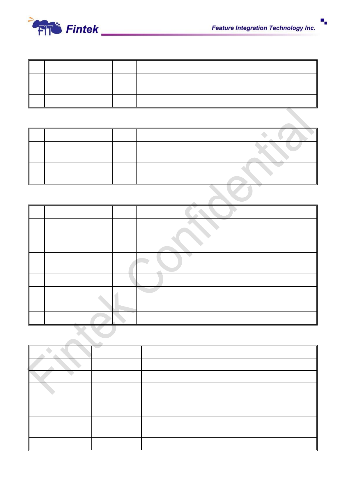
88
F71868A
6.5.45 TEMP1 Limit Hystersis Select Register Index 6Ch
Bit
Name
R/W
Default
Description
7-4
TEMP1_HYS
R/W
4h
Limit hysteresis. (0~15 degree C)
Temperature and below the (boundary – hysteresis ).
3-0
Reserved
R
0h
Reserved
Bit
Name
R/W
Default
Description
7-4
TEMP3_HYS
R/W
2h
Limit hysteresis. (0~15 degree C)
Temperature and below the ( boundary – hysteresis ).
3-0
TEMP2_HYS
R/W
4h
Limit hysteresis. (0~15 degree C)
Temperature and below the ( boundary – hysteresis ).
Bit
Name
R/W
Default
Description
7-6
Reserved
R - Reserved
5
PECI_OPEN
R
-
When PECI interface is enabled, “1” indicates an error code (0x0080
or 0x0081) is received from PECI slave.
4
TSI_OPEN
R
-
When TSI interface is enabled, “1” indicates the error of not receiving
NACK bit or a timeout occurred.
3
T3_DIODE_OPEN
R - “1” indicates external diode 3 is open
2
T2_DIODE_OPEN
R - “1” indicates external diode 2 is open or short
1
T1_DIODE_OPEN
R - “1” indicates external diode 1 is open or short
0
Reserved
R - Reserved
Address
Attribute
Default Value
Description
70h
Reserved
FFh
Reserved
71h
Reserved
FFh
Reserved
72h R --
Temperature 1 reading. The unit of reading is 1ºC.At the moment
of reading this register.
73h R --
Reserved
74h R --
Temperature 2 reading. The unit of reading is 1ºC.At the moment
of reading this register.
75h R --
Reserved
6.5.46 TEMP2 and TEMP3 Limit Hystersis Select Register Index 6Dh
6.5.47 DIODE OPEN Status Register Index 6Fh
6.5.48 Temperature Index 70h- 8Dh
May, 2015
V 0.17P
Page 89
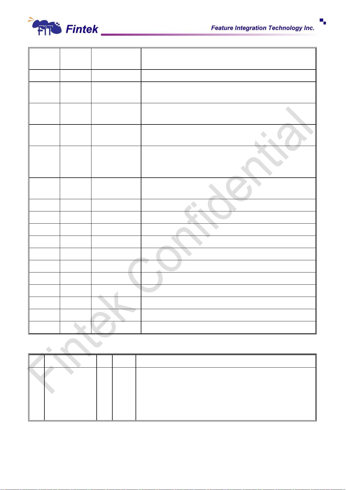
89
F71868A
76h R --
Temperature 3 reading. The unit of reading is 1ºC.At the moment
of reading this register.
77-79h R --
Reserved
7Ah R --
The data of CPU temperature from digital interface after IIR filter.
(Available if Intel IBX or AMD TSI interface is enabled)
7Bh R --
The raw data of PCH temperature from digital interface. (Only
available if Intel IBX interface is enabled)
7Ch R --
The raw data of MCH read from digital interface. (Only available if
Intel IBX interface is enabled)
7Dh R --
The raw data of maximum temperature between CPU/PCH/MCH
from digital interface. (Only available if Intel IBX interface is
enabled)
7Eh R --
The data of CPU temperature from digital interface after IIR filter.
(Only available if PECI interface is enabled)
7Fh
Reserved
FFh
Reserved
80h
Reserved
FFh
Reserved
81h
Reserved
FFh
Reserved
82h
R/W
64h
Temperature sensor 1 OVT limit. The unit is 1ºC.
83h
R/W
55h
Temperature sensor 1 high limit. The unit is 1ºC.
84h
R/W
64h
Temperature sensor 2 OVT limit. The unit is 1ºC.
85h
R/W
55h
Temperature sensor 2 high limit. The unit is 1ºC.
86h
R/W
55h
Temperature sensor 3 OVT limit. The unit is 1ºC.
87h
R/W
46h
Temperature sensor 3 high limit. The unit is 1ºC.
88-8Bh R --
Reserved
8C~8Dh R FFH
Reserved
Bit
Name
R/W
Default
Description
7-6
IIR-QUEUR3
R/W
1h
The queue time for second filter to quickly update values.
00: 8 times.
01: 12 times.
10: 16 times. (default)
11: 24 times.
6.5.49 Temperature Filter Select Register Index 8Eh
May, 2015
V 0.17P
Page 90
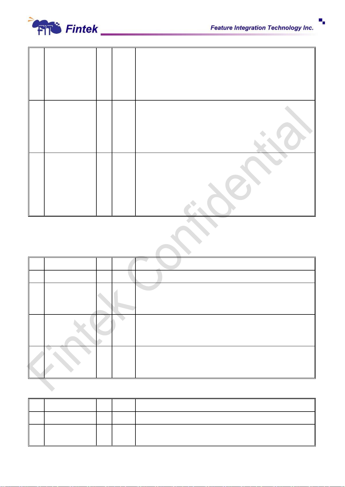
90
F71868A
5-4
IIR-QUEUR2
R/W
1h
The queue time for second filter to quickly update values.
00: 8 times.
01: 12 times.
10: 16 times. (default)
11: 24 times.
3-2
IIR-QUEUR1
R/W
1h
The queue time for second filter to quickly update values.
00: 8 timers.
01: 12 times.
10: 16 times. (default)
11: 24 times.
1-0
IIR-QUEUR_DIG
R/W
1h
The queue time for second filter to quickly update values. (for CPU
temperature from PECI or TSI interface)
00: 8 timers.
01: 12 times.
10: 16 times. (default)
11: 24 times.
Bit
Name
R/W
Default
Description
7-3
Reserved
R 0 Reserved
2
EN_FAN3_PME
R/W
0
A one enables the corresponding interrupt status bit for PME#
interrupt
Set this bit 1 to enable PME# function for Fan3.
1
EN_FAN2_PME
R/W
0
A one enables the corresponding interrupt status bit for PME#
interrupt.
Set this bit 1 to enable PME# function for Fan2.
0
EN_FAN1_PME
R/W
0
A one enables the corresponding interrupt status bit for PME#
interrupt.
Set this bit 1 to enable PME# function for Fan1.
Bit
Name
R/W
Default
Description
7-3
Reserved
R
0
Reserved
2
FAN3_STS
R/W
--
This bit is set when the fan3 count exceeds the count limit. Write 1 to
clear this bit, write 0 will be ignored.
Fan Control Setting
6.5.50 FAN PME# Enable Register Index 90h
6.5.51 FAN Interrupt Status Register Index 91h
May, 2015
V 0.17P
Page 91
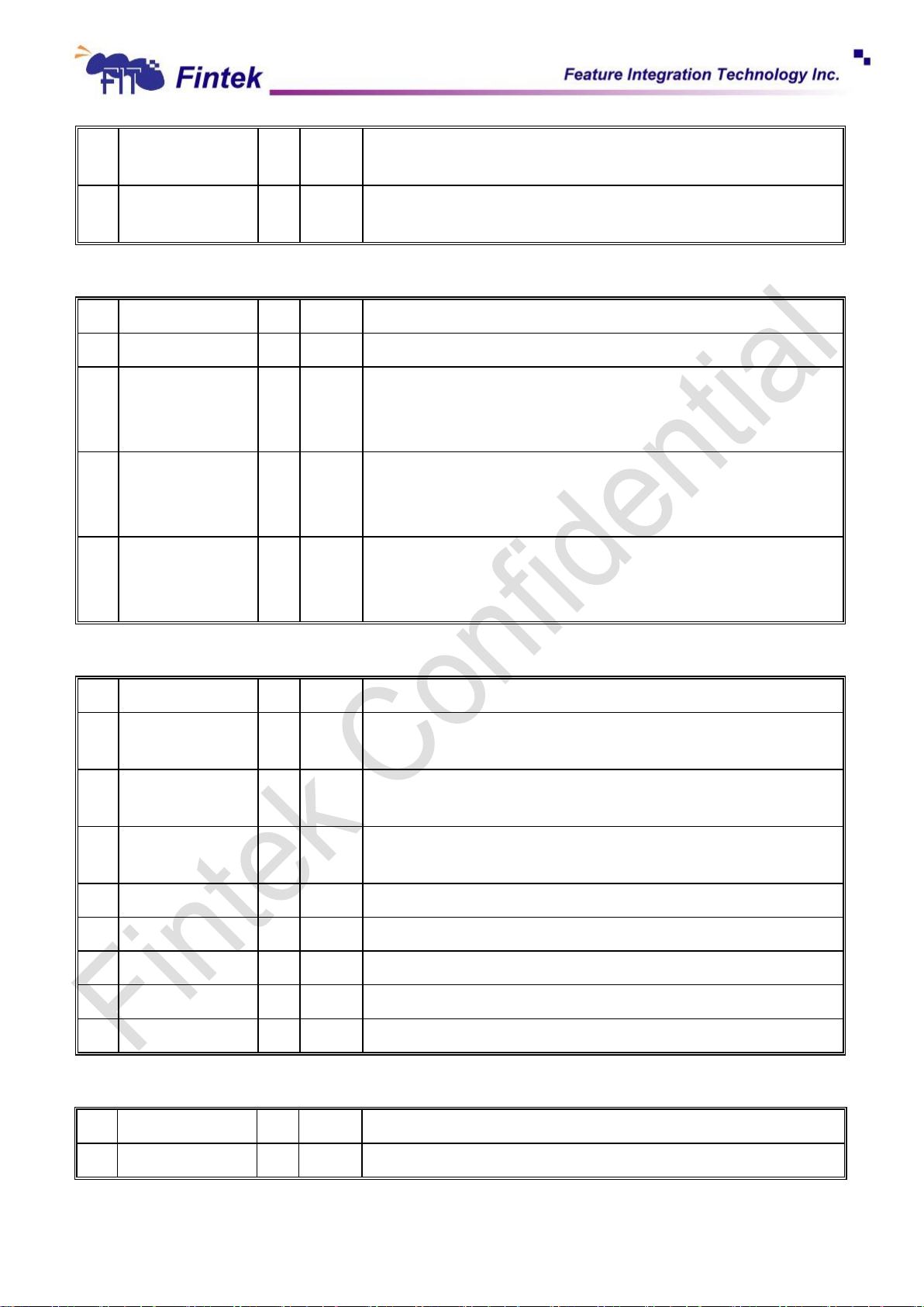
91
F71868A
1
FAN2_STS
R/W
--
This bit is set when the fan2 count exceeds the count limit. Write 1 to
clear this bit, write 0 will be ignored.
0
FAN1_STS
R/W
--
This bit is set when the fan1 count exceeds the count limit. Write 1 to
clear this bit, write 0 will be ignored.
6.5.52 FAN Real Time Status Register Index 92h
Bit
Name
R/W
Default
Description
7-3
Reserved
--
0
2
FAN3_EXC
R
--
This bit set to high mean that fan3 count can’t meet expect count over
than SMI time(CR9F) or when duty not zero but fan stop over then 3
sec.
1
FAN2_EXC
R
--
This bit set to high mean that fan2 count can’t meet expect count over
than SMI time(CR9F) or when duty not zero but fan stop over then 3
sec.
0
FAN1_EXC
R
--
This bit set to high mean that fan1 count can’t meet expect count over
than SMI time(CR9F) or when duty not zero but fan stop over then 3
sec.
Bit
Name
R/W
Default
Description
7
FULL_WITH_
T3_EN
R/W
0
Set one will enable FAN to force full speed when T3 over high limit.
6
FULL_WITH_
T2_EN
R/W
0
Set one will enable FAN to force full speed when T2 over high limit.
5
FULL_WITH_
T1_EN
R/W
0
Set one will enable FAN to force full speed when T1 over high limit.
4
Reserved
- - Reserved
3
Reserved
- - Reserved.
2
EN_FAN3_ BEEP
R/W
0
A one enables the corresponding interrupt status bit for BEEP.
1
EN_FAN2_ BEEP
R/W
0
A one enables the corresponding interrupt status bit for BEEP.
0
EN_FAN1_ BEEP
R/W
0
A one enables the corresponding interrupt status bit for BEEP.
Bit
Name
R/W
Default
Description
7-6
Reserved
- - Reserved.
6.5.53 FAN BEEP# Enable Register Index 93h
6.5.54 FAN Type Select Register Index 94h (FAN_PROG_SEL = 0)
May, 2015
V 0.17P
Page 92
92
F71868A
5-4
FAN3_TYPE
R/W
2’b 0S
00: Output PWM mode (push pull) to control fans.
01: Use linear fan application circuit to control fan speed by fan’s
power terminal.
10: Output PWM mode (open drain) to control Intel 4-wire fans.
11: Reserved.
Bit 0 is power on trap by FANCTRL3
0: FANCTRL3 is pull up by external resistor.
1: FANCTRL3 is pull down by internal 100K resistor.
3-2
FAN2_TYPE
R/W
2’b 0S
00: Output PWM mode (push pull) to control fans.
01: Use linear fan application circuit to control fan speed by fan’s
power terminal.
10: Output PWM mode (open drain) to control Intel 4-wire fans.
11: Reserved.
Bit 0 is power on trap by FANCTRL2
0: FANCTRL2 is pull up by external resistor.
1: FANCTRL2 is pull down by internal 100K resistor.
1-0
FAN1_TYPE
R/W
2’b 0S
00: Output PWM mode (push pull) to control fans.
01: Use linear fan application circuit to control fan speed by fan’s
power terminal.
10: Output PWM mode (open drain) to control Intel 4-wire fans.
11: Reserved.
Bit 0 is power on trap by FANCTRL1
0: FANCTRL1 is pull up by external resistor.
1: FANCTRL1is pull down by internal 100K resistor.
Bit
Name
R/W
Default
Description
7-0
FAN1_BASE
_TEMP
R/W
0
This register is used to set the base temperature for FAN1
temperature adjustment.
The FAN1 temperature is calculated according to the equation:
Tfan1 = Tnow + (Ta – Tb)*Ct
Where Tnow is selected by FAN1_TEMP_SEL_DIG and
FAN1_TEMP_SEL.
Tb is this register, Ta is selected by TFAN1_ADJ_SEL and Ct is
selected by TFAN1_ADJ_UP_RATE/TFAN1_ADJ_DN_RATE.
To access this register, FAN_PROG_SEL(CR9F[7]) must set to “1”.
S: Register default values are decided by trapping.
6.5.55 FAN Type Select Register Index 94h (FAN_PROG_SEL = 1)
May, 2015
V 0.17P
Page 93

93
F71868A
6.5.56 FAN1 Temperature Adjust Rate Register Index 95h (FAN_PROG_SEL = 1)
Bit
Name
R/W
Default
Description
7
Reserved
- - Reserved
6-4
TFAN1_ADJ_UP
_RATE
3’h0
This selects the weighting of the difference between Ta and Tb if Ta is
higher than Tb.
3’h1: 1 (Ct = 1)
3’h2: 1/2 (Ct= 1/2)
3’h3: 1/4 (Ct = 1/4)
3’h4: 1/8 (Ct = 1/8)
otherwise: 0
To access this byte, FAN_PROG_SEL must set to “1”.
3
Reserved
- - Reserved
2-0
TFAN1_ADJ_DN
_RATE
R/W
3’h0
This selects the weighting of the difference between Ta and Tb if Ta is
lower than Tb.
3’h1: 1 (Ct = 1)
3’h2: 1/2 (Ct= 1/2)
3’h3: 1/4 (Ct = 1/4)
3’h4: 1/8 (Ct = 1/8)
otherwise: 0
To access this byte, FAN_PROG_SEL must set to “1”.
Bit
Name
R/W
Default
Description
7-6
Reserved
- - Reserved
5-4
FAN3_MODE
R/W
01
00: Auto fan speed control. Fan speed will follow different temperature
by different RPM defined in 0xC6-0xCE.
01: Auto fan speed control. Fan speed will follow different temperature
by different duty cycle defined in 0xC6-0xCE.
10: Manual mode fan control. User can write expected RPM count to
0xC2-0xC3, and F71868A will adjust duty cycle (PWM fan type) or
voltage (linear fan type) to control fan speed automatically.
11: Manual mode fan control. User can write expected duty cycle
(PWM fan type) or voltage (linear fan type) to 0xC3, and F71868A will
output this desired duty or voltage to control fan speed.
6.5.57 FAN mode Select Register Index 96h (FAN_PROG_SEL = 0)
May, 2015
V 0.17P
Page 94

94
F71868A
3-2
FAN2_MODE
R/W
01
00: Auto fan speed control. Fan speed will follow different temperature
by different RPM defined in 0xB6-0xBE.
01: Auto fan speed control. Fan speed will follow different temperature
by different duty cycle (voltage) defined in 0xB6-0xBE.
10: Manual mode fan control. User can write expected RPM count to
0xB2-0xB3, and F71868A will adjust duty cycle (PWM fan type) or
voltage (linear fan type) to control fan speed automatically.
11: Manual mode fan control, user can write expected duty cycle
(PWM fan type) or voltage (linear fan type) to 0xB3, and F71868A will
output this desired duty or voltage to control fan speed.
1-0
FAN1_MODE
R/W
01
00: Auto fan speed control. Fan speed will follow different temperature
by different RPM defined in 0xA6-0xAE.
01: Auto fan speed control. Fan speed will follow different temperature
by different duty cycle defined in 0xA6-0xAE.
10: Manual mode fan control, user can write expected RPM count to
0xA2-0xA3, and F71868A will auto control duty cycle (PWM fan type)
or voltage (linear fan type) to control fan speed automatically.
11: Manual mode fan control, user can write expected duty cycle
(PWM fan type) or voltage (linear fan type) to 0xA3, and F71868A will
output this desired duty or voltage to control fan speed.
Bit
Name
R/W
Default
Description
7-3
Reserved
- - Reserved
2-0
TFAN1_ADJ_SEL
R/W
0h
This selects which temperature to be used as Ta for Fan1 temperature
adjustment.
000: PECI (CR7Eh)
001: T1 (CR72h)
010: T2 (CR74h)
011: T3 (CR76h)
100: Digital T1 (CR7Ah)
101: Digital T1 (CR7Bh)
110: Digital T2 (CR7Ch)
111: Digital T3 (CR7Dh)
otherwise: Ta will be 0.
To access this register FAN_PROG_SEL must set to “1”.
6.5.58 FAN mode Select Register Index 96h (FAN_PROG_SEL = 1)
May, 2015
V 0.17P
Page 95
95
F71868A
6.5.59 Auto FAN1 and FAN2 Boundary Hystersis Select Register Index 98h
Bit
Name
R/W
Default
Description
7-4
FAN2_HYS
R/W
4h
Boundary hysteresis. (0~15 degree C)
Segment will change when the temperature over the boundary
temperature and below the ( boundary – hysteresis ).
3-0
FAN1_HYS
R/W
4h
Boundary hysteresis. (0~15 degree C)
Segment will change when the temperature over the boundary
temperature and below the ( boundary – hysteresis ).
Bit
Name
R/W
Default
Description
7-4
Reserved
- - Reserved.
3-0
FAN3_HYS
R/W
2h
Boundary hysteresis. (0~15 degree C)
Segment will change when the temperature over the boundary
temperature and below the ( boundary – hysteresis ).
Bit
Name
R/W
Default
Description
7
Reserved
- - Reserved.
6
R/W
0
This bit and FAN3_PWM_FREQ_SEL are used to select FAN3 PWM
frequency. NEW_FREQ_SEL3 = { FREQ_SEL_ADD3,
FAN3_PWM_FREQ_SEL}
00: 23.5 KHz
01: 220 Hz
10: 11.75 KHz
11: 5.875 KHz
5
R/W
0
This bit and FAN2_PWM_FREQ_SEL are used to select FAN2 PWM
frequency. NEW_FREQ_SEL2 = { FREQ_SEL_ADD2,
FAN2_PWM_FREQ_SEL}
00: 23.5 KHz
01: 220 Hz
10: 11.75 KHz
11: 5.875 KHz
6.5.60 Auto FAN3 Boundary Hystersis Select Register Index 99h
6.5.61 Fan3 Control Register Index 9Ah
May, 2015
V 0.17P
Page 96
96
F71868A
4
R/W
0
This bit and FAN1_PWM_FREQ_SEL are used to select FAN1 PWM
frequency. NEW_FREQ_SEL1 = { FREQ_SEL_ADD1,
FAN1_PWM_FREQ_SEL}
00: 23.5 KHz
01: 220 Hz
10: 11.75 KHz
11: 5.875 KHz
3-2
Reserved
R/W
0
Reserved (Keep the value of these two bits “0”)
1
Reserved
R/W
1
Reserved (Keep the value of this bit “1”)
0
Reserved
R/W
0
Reserved
6.5.62 Auto Fan Up Speed Update Rate Select Register Index 9Bh (FAN_PROG_SEL = 0)
Bit
Name
R/W
Default
Description
7-6
Reserved
- - Reserved.
5-4
FAN3_UP_RATE
R/W
01
Fan3 duty update rate:
00: 2Hz
01: 5Hz (default)
10: 10Hz
11: 20Hz
3-2
FAN2_UP_RATE
R/W
01
Fan2 duty update rate:
00: 2Hz
01: 5Hz (default)
10: 10Hz
11: 20Hz
1-0
FAN1_UP_RATE
R/W
01
Fan1 duty update rate:
00: 2Hz
01: 5Hz (default)
10: 10Hz
11: 20Hz
Bit
Name
R/W
Default
Description
7
UP_DN_RATE_EN
R/W
0
0: Fan down rate disable
1: Fan down rate enable
6
DIRECT_LOAD_EN
R/W
0
0: Direct load disable
1: Direct load enable for manual duty mode
6.5.1 Auto Fan Up Speed Update Rate Select Register Index 9Bh (FAN_PROG_SEL = 1)
May, 2015
V 0.17P
Page 97
97
F71868A
5-4
FAN3_DN_RATE
R/W
01
Fan3 duty update rate:
00: 2Hz
01: 5Hz (default)
10: 10Hz
11: 20Hz
3-2
FAN2_DN_RATE
R/W
01
Fan2 duty update rate:
00: 2Hz
01: 5Hz (default)
10: 10Hz
11: 20Hz
1-0
FAN1_DN_RATE
R/W
01
Fan1 duty update rate:
00: 2Hz
01: 5Hz (default)
10: 10Hz
11: 20Hz
Bit
Name
R/W
Default
Description
7-4
FAN2_STOP
_DUTY
R/W
5h
When fan start, the FAN_CTRL2 will increase duty-cycle from 0 to this
(value x 8) directly. And if fan speed is down, the FAN_CTRL 2 will
decrease duty-cycle to 0 when the PWM duty cycle is less than this
(value x 4).
3-0
FAN1_STOP
_DUTY
R/W
5h
When fan start, the FAN_CTRL 1 will increase duty-cycle from 0 to
this (value x 8 directly. And if fan speed is down, the FAN_CTRL 1 will
decrease duty-cycle to 0 when the PWM duty cycle is less than this
(value x 4).
Bit
Name
R/W
Default
Description
7-4
Reserved
- - Reserved.
3-0
FAN3_STOP_
DUTY
R/W
5h
When fan start, the FAN_CTRL 3 will increase duty-cycle from 0 to
this (value x 8 directly. And if fan speed is down, the FAN_CTRL 3 will
decrease duty-cycle to 0 when the PWM duty cycle is less than this
(value x 4).
6.5.2 FAN1 and FAN2 START UP DUTY-CYCLE/VOLTAGE Index 9Ch
6.5.3 FAN3 START UP DUTY-CYCLE/VOLTAGE Index 9Dh
May, 2015
V 0.17P
Page 98
98
F71868A
6.5.4 FAN PROGRAMMABLE DUTY-CYCLE/VOLTAGE LOADED AFTER POWER-ON Index 9Eh
Bit
Name
R/W
Default
Description
7-0
PROG_DUTY_VAL
R/W
66h
This byte will be immediately loaded as Fan duty value after VDD is
powered on if it has been programmed before shut down.
Bit
Name
R/W
Default
Description
7
FAN_PROG_SEL
R/W
0
Set this bit to “1” will enable accessing registers of other bank.
6
FAN_MNT_SEL
R/W
0
Set this bit to monitor a slower fan.
5
Reserved
- - Reserved
4
FULL_DUTY_SEL
R/W
-
0: The Fan Duty is 100% and will be loaded immediately after VDD is
powered on if CR9E is not been programmed before shut down. (pull
down by external resistor)
1: The Fan Duty is 40% and will be loaded immediately after VDD is
powered on if CR9E is not been programmed before shut down. (pull
up by internal 47K resistor).
This register is power on trap by DTR1#.
3-0
F_FAULT_TIME
R/W
Ah
This register determines the time of fan fault. The condition to cause
fan fault event is:
When PWM_Duty reaches FFh, if the fan speed count can’t reach the
fan expect count in time.
The unit of this register is 1 second. The default value is 11 seconds.
(Set to 0 , means 1 seconds. ; Set to 1, means 2 seconds.
Set to 2, means 3 seconds. …. )
Another condition to cause fan fault event is fan stop and the PWM
duty is greater than the minimum duty programmed by the register
index 9C-9Dh.
Address
Attribute
Default Value
Description
A0h
RO
8’h0f
FAN1 count reading (MSB). At the moment of reading this register,
the LSB will be latched. This will prevent from data updating when
reading. To read the fan count correctly, read MSB first and followed
read the LSB.
A1h
RO
8’hff
FAN1 count reading (LSB).
A2h
R/W
8’h00
RPM mode(CR96 bit0=0):
FAN1 expect speed count value (MSB), in auto fan mode (CR96
6.5.5 Fan Fault Time Register Index 9Fh
6.5.6 FAN1 Index A0h~AFh
May, 2015
V 0.17P
Page 99
99
F71868A
bit10) this register is auto updated by hardware.
Duty mode(CR96 bit0=1):
This byte is reserved byte.
A3h
R/W
8’h01
RPM mode(CR96 bit0=0):
FAN1 expect speed count value (LSB) or expect PWM duty, in auto
fan mode this register is auto updated by hardware and read only.
Duty mode(CR96 bit0=1):
The Value programming in this byte is duty value. In auto fan mode
(CR96 bit10) this register is updated by hardware.
Ex: 5 5*100/255 %
255 100%
A4h
R/W
8’h03
FAN1 full speed count reading (MSB). At the moment of reading this
register, the LSB will be latched. This will prevent from data
updating when reading. To read the fan count correctly, read MSB
first and followed read the LSB.
A5h
R/W
8’hff
FAN1 full speed count reading (LSB).
Bit
Name
R/W
Default
Description
7-0
BOUND1TMP1
R/W
3Ch
(60oC)
The first boundary temperature for VT1 in temperature mode.
When VT1 temperature exceeds this boundary, expected FAN1 value
will be loaded from segment 1 register (index AAh).
When VT1 temperature is under this boundary – hysteresis, expected
FAN1 value will be loaded from segment 2 register (index ABh).
This byte is a 2’s complement value ranged from -128’C ~ 127’C.
Bit
Name
R/W
Defaul
t
Description
7-0
BOUND2TMP1
R/W
32
(50ºC)
The 2nd BOUNDARY temperature for VT1 in temperature mode.
When VT1 temperature is exceed this boundary, FAN1 expected
value will load from segment 2 register (index ABh).
When VT1 temperature is below this boundary – hysteresis, FAN1
expected value will load from segment 3 register (index ACh).
This byte is a 2’s complement value ranging from -128ºC ~ 127ºC.
Bit
Name
R/W
Defaul
t
Description
6.5.7 VT1 BOUNDARY 1 TEMPERATURE – Index A6h
6.5.8 VT1 BOUNDARY 2 TEMPERATURE – Index A7
6.5.9 VT1 BOUNDARY 3 TEMPERATURE – Index A8h
May, 2015
V 0.17P
Page 100
100
F71868A
7-0
BOUND3TMP1
R/W
28h
(40ºC)
The 3rd BOUNDARY temperature for VT1 in temperature mode.
When VT1 temperature is exceed this boundary, FAN1 expected
value will load from segment 3 register (index ACh).
When VT1 temperature is below this boundary – hysteresis, FAN1
expected value will load from segment 4 register (index ADh).
This byte is a 2’s complement value ranging from -128ºC ~ 127ºC.
6.5.10 VT1 BOUNDARY 4 TEMPERATURE – Index A9
Bit
Name
R/W
Defaul
t
Description
7-0
BOUND4TMP1
R/W
1Eh
(30ºC)
The 4th BOUNDARY temperature for VT1 in temperature mode.
When VT1 temperature is exceed this boundary, FAN1 expected
value will load from segment 4 register (index ADh).
When VT1 temperature is below this boundary – hysteresis, FAN1
expected value will load from segment 5 register (index AEh).
This byte is a 2’s complement value ranging from -128ºC ~ 127ºC.
Bit
Name
R/W
Default
Description
7-0
SEC1SPEED1
R/W
FFh
(100%)
The meaning of this register is depending on the FAN1_MODE(CR96)
2’b00: The value that set in this byte is the relative expect fan speed
% of the full speed in this temperature section.
Ex:
100%:full speed: User must set this register to 0.
60% full speed: (100-60)*32/60, so user must program 21 to this reg.
X% full speed: The value programming in this byte is ( (100-X)*32/X
2’b01: The value that set in this byte is mean the expect PWM
duty-cycle in this temperature section.
Bit
Name
R/W
Default
Description
7-0
SEC2SPEED1
R/W
D9h
(85%)
The meaning of this register is depending on the FAN1_MODE(CR96)
2’b00: The value that set in this byte is the relative expect fan speed
% of the full speed in this temperature section.
2’b01: The value that set in this byte is mean the expect PWM
duty-cycle in this temperature section.
Bit
Name
R/W
Default
Description
6.5.11 FAN1 SEGMENT 1 SPEED COUNT – Index AAh
6.5.12 FAN1 SEGMENT 2 SPEED COUNT – Index ABh
6.5.13 FAN1 SEGMENT 3 SPEED COUNT Register – Index ACh
May, 2015
V 0.17P
 Loading...