

Page 1

F71805F/FG
F71805
Super H/W Monitor + LPC IO
Release Date: Dec., 2006
Revision: V0.25P
F71805 Dec., 2006
V0.25P
Page 2

F71805 Datasheet Revision History
F71805
Version Date Page Revision History
0.20P 07/07/2004 - Preliminary Release Version.
0.21P 07/28/2004 Revised PWM frequency range.
0.22P 10/12/2004 10 Added FANCTL Functions.
22 Revised Voltage Fault Enable Register (Index 29h bit 7).
- Modified Application Circuit.
0.23P 04/15/2005 91 Added “Green Package” ordering information
0.24P 09/05/2006 16 Modified typo.
- Added PWM Output frequency setting description.
0.25P 12/28/2006 4 Added Patent Note.
Please note that all data and specifications are subject to change without notice. All the trade marks of products and
companies mentioned in this data sheet belong to their respective owners.
LIFE SUPPORT APPLICATIONS
These products are not designed for use in life support appliances, devices, or systems where malfunction of these
products can reasonably be expected to result in personal injury. Customers using or selling these products for use
in such applications do so at their own risk and agree to fully indemnify Fintek for any damages resulting from such
improper use or sales.
F71805 Dec., 2006
V0.25P
Page 3

F71805
Table of Contents
1. GENERAL DESCRIPTION.........................................................................................................................................................3
2. FEATURES....................................................................................................................................................................................3
3. KEY SPECIFICATIONS..............................................................................................................................................................5
4. PIN CONFIGURATI ON...............................................................................................................................................................5
5. PIN DESCRIPTION......................................................................................................................................................................6
5.1 POWER PIN.........................................................................................................................................................................6
5.2 LPC INTERFACE.................................................................................................................................................................6
5.3 FDC...................................................................................................................................................................................7
5.4 UART PORT AND SIR.........................................................................................................................................................7
5.5 IEEE 1284 PARALLEL PORT ...............................................................................................................................................9
5.6 H/W MONITOR...................................................................................................................................................................9
5.7 FLASH ROM INTERF ACE AND GPIO.................................................................................................................................10
6. FUNCTION DESCRIPTION .....................................................................................................................................................11
6.1 POWER ON STRAPPING OPTIONS.......................................................................................................................................11
6.2 HARDWARE MONITOR......................................................................................................................................................11
6.3 FDC.................................................................................................................................................................................18
6.4 UART..............................................................................................................................................................................19
6.5 PARALLEL PORT ...............................................................................................................................................................19
7. REGISTER DESCRIPTION......................................................................................................................................................19
7.1 GLOBAL CONTROL REGISTERS.........................................................................................................................................19
7.1.1 Software Reset Register Index 02h............................................................................................................................20
7.1.2 Logic Device Number Register Index 07h................................................................................................................. 20
7.1.3 Chip ID Register Index 20h....................................................................................................................................... 20
7.1.4 Chip ID Register Index 21h....................................................................................................................................... 20
7.1.5 Vendor ID Register Index 23h ...................................................................................................................................20
7.1.6 Vendor ID Register Index 24h ...................................................................................................................................20
7.1.7 Software Power Down Register Index 25h................................................................................................................ 20
7.1.8 UART IRQ Sharing Register Index 26h ....................................................................................................................21
7.1.9 Power On Trap Status Register Index 27h.................................................................................................................21
7.1.10 Flash Control Register Index 28h ..............................................................................................................................21
7.1.11 Voltage Fault Enable Register Index 29h...................................................................................................................22
1
Dec., 2006
V0.25P
Page 4

F71805
7.2 FDC REGISTER.................................................................................................................................................................22
7.2.1 Logic Device Number Register........................................................................................................................................22
7.2.2 FDC Configuration Registers........................................................................................................................................... 23
7.2.3 Device Registers..............................................................................................................................................................25
7.3 UART 1 REGISTER ...........................................................................................................................................................40
7.3.1 Logic Device Number Register........................................................................................................................................40
7.3.2 UART 1 Configuration Register.......................................................................................................................................41
7.3.3 Device Registers..............................................................................................................................................................42
7.4 UART 2 REGISTER ...........................................................................................................................................................45
7.4.1 Logic Device Number Register........................................................................................................................................45
7.4.2 UART 2 Configuration Registers..................................................................................................................................... 45
7.4.3 Device Registers..............................................................................................................................................................47
7.5 PARALLEL PORT REGISTER ...............................................................................................................................................50
7.5.1 Logic Device Number Register........................................................................................................................................50
7.5.2 Parallel Port Configuration Registers...............................................................................................................................50
7.5.3 Device Registers..............................................................................................................................................................51
7.6 HARDWARE MONITOR REGISTER ..................................................................................................................................... 55
7.6.1 Logic Device Number Registers...................................................................................................................................... 55
7.6.2 Hardware Monitor Configuration Registers..................................................................................................................... 55
7.6.3 Device Registers..............................................................................................................................................................56
7.7 GPIO REGISTER...............................................................................................................................................................76
7.7.1 Logic Device Number Register........................................................................................................................................76
7.7.2 GPIO Configuration Registers......................................................................................................................................... 76
7.8 PME REGISTER ................................................................................................................................................................83
7.8.1 Logic Device Number Register........................................................................................................................................83
7.8.2 PME Configuration Registers..........................................................................................................................................83
8. PCB LAYOUT GUIDE................................................................................................................................................................85
9. ELECTRICAL CHARACTERISTIC........................................................................................................................................86
9.1 ABSOLUTE MAXIMUM RATIN GS .......................................................................................................................................86
9.2 DC CHARACTERISTICS.....................................................................................................................................................86
9.3 AC CHARACTERISTICS.....................................................................................................................................................87
10. ORDERING INFORMATION................................................................................................................................................87
11. PACKAGE DIMENSIO NS......................................................................................................................................................88
12. F71805 DEMO CIRCUIT........................................................................................................................................................89
2
Dec., 2006
V0.25P
Page 5

1. General Description
The F71805 is the featured IO chip specifically for PC system. Equipped with one IEEE 1284
parallel port, two UART port and FDC, F71805 provides SIR and Flash ROM Interface. Integrated with
hardware monitor, F71805 supports 9 sets of voltage sensor and 4 voltage fault signal outputs, 3 sets of
creative auto-controlling fans and 3 temperature sensor pins for the accurate current type temp.
measurement for CPU thermal diode or external transistors 2N3906.
The F71805 provides flexible features for multi-directional application. For instance, supports 24
GPIO pins which include pulse/level mode selection, IRQ sharing function also designed in UART
feature for particular usage and accurate current mode H/W monitor will be worth in measurement of
F71805
temperature. The F71805 is powered by 3.3V voltage, with the LPC interface in the package of 128-QFP.
2. Features
General Functions
¾ Comply with LPC Spec. 1.0
¾ Supports 24 GPIO pins. One set of GPIO supports High/Low Level/Pulse selection.
¾ 48 MHz clock input
FDC
¾ Compatible with IBM PC AT disk drive systems
¾ Variable write pre-compensation with track selectable capability
¾ Support vertical recording format
¾ DMA enable logic
¾ 16-byte data FIFOs
¾ Support floppy disk drives and tape drives
¾ Detects all overrun and under run conditions
¾ Built-in address mark detection circuit to simplify the read electronics
¾ Completely compatible with industry standard 82077
¾ 360K/720K/1.2M/1.44M/2.88M format; 250K, 300K, 500K, 1M, 2M bps data transfer rate
¾ Support 3-mode FDD, and its Win95/98/2K/XP driver
UART
¾ Two high-speed 16C550 compatible UART with 16-byte FIFOs
¾ Fully programmable serial-interface characteristics
3
Dec., 2006
V0.25P
Page 6

Infrared
Flash ROM Interface
Parallel Port
F71805
¾ Baud rate up to 115.2K
¾ Support IrDA version 1.0 SIR protocol with maximum baud rate up to 115.2K bps
¾ Up to 4M bits flash ROM supported
¾ One PS/2 compatible bi-directional parallel port
¾ Support Enhanced Parallel Port (EPP) − Compatible with IEEE 1284 specification
¾ Support Extended Capabilities Port (ECP) − Compatible with IEEE 1284 specification
¾ Enhanced printer port back-drive current protection
Hardware Monitor Functions
¾ 3 current type accurate (±3) ℃ thermal inputs for CPU thermal diode and 2N3906 transistors
¾ 9 voltage monitoring inputs (8 external and Vcc power)
¾ 4 voltage_fault# hardware signal outputs
¾ 3 fan speed monitoring inputs
¾ 3 fan speed auto-control --- support 3 wire and 4 wire fans
¾ WATCHDOG comparison of all monitored values
¾ Issue PME#, OVT# and independent Voltage_fault #
Package
¾ 128-pin PQFP
Noted: Patented TW207103 TW207104 US6788131 B1 TW235231 TW237183 TWI263778
4
Dec., 2006
V0.25P
Page 7
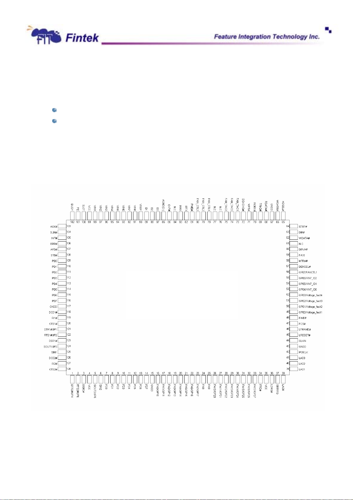
3. Key Specifications
Supply Voltage 3.0V to 3.6V
Operating Supply Current 5 mA typ.
4. Pin Configuration
F71805
F71805
Figure 1
5
Dec., 2006
V0.25P
Page 8

5. Pin Description
I/O
- TTL level bi-directional pin with 12 mA source-sink cap ability.
12t
I/OOD
I/OOD
- TTL level bi-directional pin, can select to OD or OUT by register, with 12 mA source-sink
12t
capability.
- TTL level bi-directional pin, can select to OD or OUT by register, with 16 mA source-sink
16t
capability.
F71805
I/OD
I/O8t
I/O
8t-u47,5V
I/O
12ts5V
O
12
O8
12ts5V
- TTL level bi-directional pin and schmitt trigger, Open-drain output with 12 mA sink capability,
5V tolerance.
- TTL level bi-directional pin with 8 mA sink capability.
- TTL level bi-directional pin with 8 mA sink capability, pull-up 47k ohms, 5V tolerance.
- TTL level bi-directional pin and schmitt trigger with 12 mA sink capability, 5V tolerance.
- Output pin with 12 mA source-sink capability.
- Output pin with 8 A source-sink capability.
AOUT - Output pin(Analog).
OD
OD
IN
ts
IN
t5V
IN
ts5V
AIN
12
24
- Open-drain output pin with 12 mA sink capability.
- Open-drain output pin with 24 mA sink capability.
- TTL level input pin and schmitt trigger.
- TTL level input, 5V tolerance.
- TTL level input pin and schmitt trigger, 5V tolerance.
- Input pin(Analog).
P - Power.
5.1 Power Pin
Pin No. Pin Name Type Description
4,35,99 VCC P Power supply voltage input with 3.3V
86 AGND(D-) P Analog GND
15,43,67,117 GNDD P Digital GND
5.2 LPC Interface
Pin No. Pin Name Type PWR Description
45 LRESET# INts VCC Reset signal. It can connect to PCIRST# signal on the host.
36 LDRQ# O12 VCC Encoded DMA Request signal.
37 SERIRQ I/O
46 LFRAM# INts VCC Indicates start of a new cycle or termination of a broken
VCC Serial IRQ input/Output.
12t
6
Dec., 2006
V0.25P
Page 9
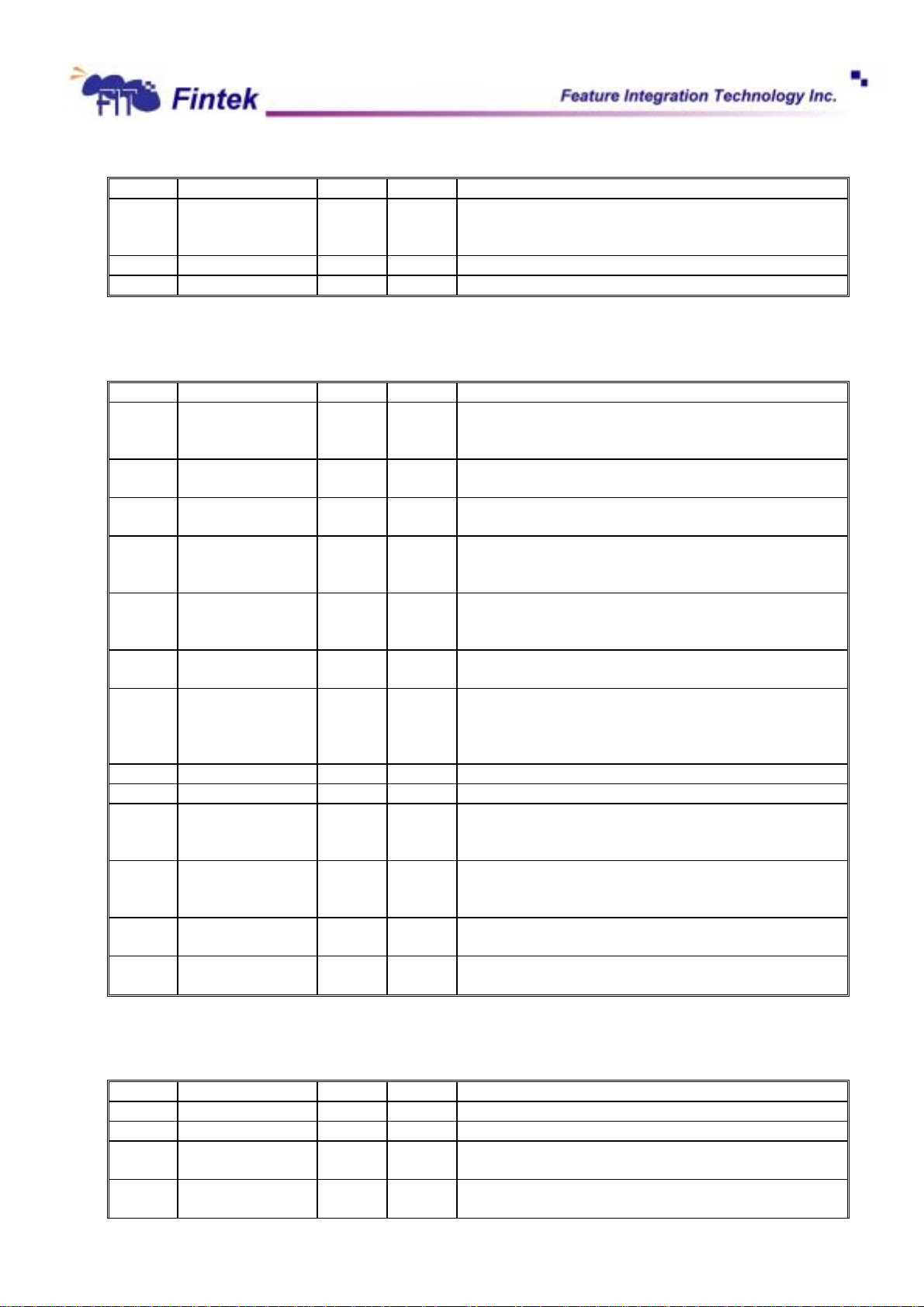
41-38 LAD[3:0] I/O
42 PCICLK INts VCC PCI clock input.
44 CLKIN INts VCC System clock input. According to the input frequency 48MHz.
5.3 FDC
Pin No. Pin Name Type PWR Description
57
58
60 DRVA# OD24 VCC Drive Select A. When set to 0, this pin enables disk drive A.
62 WDATA# OD24 VCC Write data. This logic low open drain writes
63 DIR# OD24 VCC Direction of the head step motor. An open drain output.
64 STEP# OD24 VCC Step output pulses. This active low open drain output
65 HDSEL# OD24 VCC Head select. This open drain output determines which disk
66 WGATE# OD24 VCC Write enable. An open drain output.
68 RDATA# IN
69 TRK0# IN
70 INDEX# IN
71 WPT# IN
72 DSKCHG# IN
DENSEL#
MTRA#
OD24 VCC Motor A On. When set to 0, this pin enables disk drive 0.
F71805
cycle.
VCC These signal lines communicate address, control, and data
12t
information over the LPC bus between a host and a
peripheral.
OD24 VCC Drive Density Select.
Set to 1 - High data rate.(500Kbps, 1Mbps)
Set to 0 – Low data rate. (250Kbps, 300Kbps)
This is an open drain output.
This is an open drain output.
pre-compensation serial data to the selected FDD. An open
drain output.
Logic 1 = outward motion
Logic 0 = inward motion
produces a pulse to move the head to another track.
drive head is active.
Logic 1 = side 0
Logic 0 = side 1
VCC The read data input signal from the FDD.
ts5V
VCC Track 0. This Schmitt-triggered input from the disk drive is
ts5V
active low when the head is positioned over the outermost
track.
VCC This Schmitt-triggered input from the disk drive is active low
ts5V
when the head is positioned over the beginning of a track
marked by an index hole.
VCC Write protected. This active low Schmitt input from the disk
ts5V
drive indicates that the diskette is write-protected.
VCC Diskette change. This signal is active low at power on and
ts5V
whenever the diskette is removed.
5.4 UART Port and SIR
Pin No. Pin Name Type PWR Description
82 IRTX O12 VCC Infrared Transmitter Output.
83 IRRX INts VCC Infrared Receiver input.
118 DCD1# IN
119 RI1# IN
VCC Data Carrier Detect. An active low signal indicates the
t5V
modem or data set has detected a data carrier.
VCC Ring Indicator. An active low signal indicates that a ring
t5V
signal is being received from the modem or data set.
7
Dec., 2006
V0.25P
Page 10

F71805
120 CTS1# IN
121 DTR1#/JP1 I/O
122 RTS1#/JP2 I/O
123 DSR1# IN
124 SOUT1/JP3
I/O
125 SIN1 IN
126 DCD2# IN
127 RI2# IN
128 CTS2# IN
1 DTR2#/JP4 I/O
2 RTS2#/JP6 I/O
3 DSR2# IN
5 SOUT2/JP5
I/O
6 SIN2 IN
VCC Clear To Send is the modem control input.
t5V
8t-u47,5V
VCC
UART 1 Data Terminal Ready. An active low signal informs
the modem or data set that controller is ready to
communicate. (Internal 47k pulled high and disable after
power on strapping)
Power on strapping: Default is high. Flash Rom Interface
Address Segment 1 Enable (FFFC0000h-FFFFFFFFh,
000E0000h-000FFFFFh).
(000E0000h-000EFFFFh Can be disabled by register change.)
8t-u47,5V
VCC
UART 1 Request To Send. An active low signal informs the
modem or data set that the controller is ready to send
data.(Internal 47k pulled high and disable after power on
strapping)
Power on strapping: Default is high. Flash Rom Interface
Address Segment 2 Enable (FFEE0000h-FFEFFFFFh).
VCC Data Set Ready. An active low signal indicates the modem
t5V
or data set is ready to establish a communication link and
transfer data to the UART.
8t-u47,5V
VCC
UART 1 Serial Output. Used to transmit serial data out to
the communication link.( Internal 47k pulled high and disable
after power on strapping )
Power on strapping: Default is high. Flash Rom Interface
Address Segment 3 Enable (FFF80000h-FFFBFFFFh).
VCC Serial Input. Used to receive serial data through the
t5V
communication link.
VCC Data Carrier Detect. An active low signal indicates the
t5V
modem or data set has detected a data carrier.
VCC Ring Indicator. An active low signal indicates that a ring
t5V
signal is being received from the modem or data set.
VCC Clear To Send is the modem control input.
t5V
8t-u47,5V
VCC
UART 2 Data Terminal Ready. An active low signal informs
the modem or data set that controller is ready to
communicate.( Internal 47k pulled high and disable after
power on strapping )
Power on strapping : 1 PWM Mode (Default)
0 Linear Mode
8t-u47,5V
VCC
UART 2 Request To Send. An active low signal informs the
modem or data set that the controller is ready to send
data.(Internal 47k pulled high and disable after power on
strapping )
Power on strapping : 1 XBUS Interface (Default)
0 Reserved.
VCC Data Set Ready. An active low signal indicates the modem
t5V
or data set is ready to establish a communication link and
transfer data to the UART.
8t-u47,5V
VCC
UART 2 Serial Output. Used to transmit serial data out to
the communication link.(Internal 47k pulled high and disable
after power on strapping )
Power on strapping : 1 Configuration register:4E (Default)
0 C
onfiguration register:2E
VCC Serial Input. Used to receive serial data through the
t5V
communication link.
8
Dec., 2006
V0.25P
Page 11
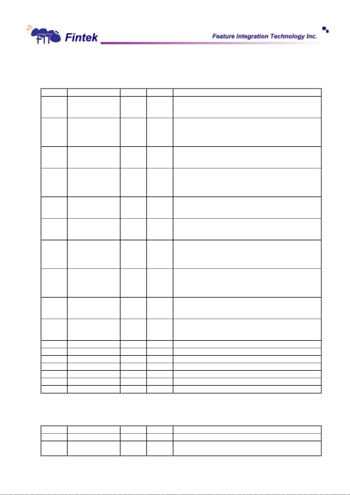
5.5 IEEE 1284 Parallel Port
Pin No. Pin Name Type PWR Description
100 SLCT IN
101 PE IN
102 BUSY IN
103 ACK# IN
104 SLIN# I/OD
105 INIT#
106 ERR#
107 AFD# I/OD
108 STB# I/OD
109
110
111
112
113
114
115
116
I/O
PD0
I/O
PD1
I/O
PD2
I/O
PD3
I/O
PD4
I/O
PD5
I/O
PD6
I/O
PD7
F71805
VCC An active high input on this pin indicates that the printer is
ts5V
selected. Refer to the description of the parallel port for
definition of this pin in ECP and EPP mode.
VCC An active high input on this pin indicates that the printer has
ts5V
detected the end of the paper. Refer to the description of the
parallel port for the definition of this pin in ECP and EPP
mode.
VCC An active high input indicates that the printer is not ready to
ts5V
receive data. Refer to the description of the parallel port for
definition of this pin in ECP and EPP mode.
VCC An active low input on this pin indicates that the printer has
ts5V
received data and is ready to accept more data. Refer to the
description of the parallel port for the definition of this pin in
ECP and EPP mode.
VCC Output line for detection of printer selection. Refer to the
12ts5V
description of the parallel port for the definition of this pin in
ECP and EPP mode.
I/OD
IN
ts5V
12ts5V
12ts5V
12ts5V
12ts5V
12ts5V
12ts5V
12ts5V
12ts5V
VCC Output line for the printer initialization. Refer to the
12ts5V
description of the parallel port for the definition of this pin in
ECP and EPP mode.
VCC An active low input on this pin indicates that the printer has
encountered an error condition. Refer to the description of
the parallel port for the definition of this pin in ECP and EPP
mode.
VCC An active low output from this pin causes the printer to auto
12ts5V
feed a line after a line is printed. Refer to the description of
the parallel port for the definition of this pin in ECP and EPP
mode.
VCC An active low output is used to latch the parallel data into the
12ts5V
printer. Refer to the description of the parallel port for the
definition of this pin in ECP and EPP mode.
VCC Parallel port data bus bit 0. Refer to the description of the
parallel port for the definition of this pin in ECP and EPP
mode.
VCC Parallel port data bus bit 1.
VCC Parallel port data bus bit 2.
VCC Parallel port data bus bit 3.
VCC Parallel port data bus bit 4.
VCC Parallel port data bus bit 5.
VCC Parallel port data bus bit 6.
VCC Parallel port data bus bit 7.
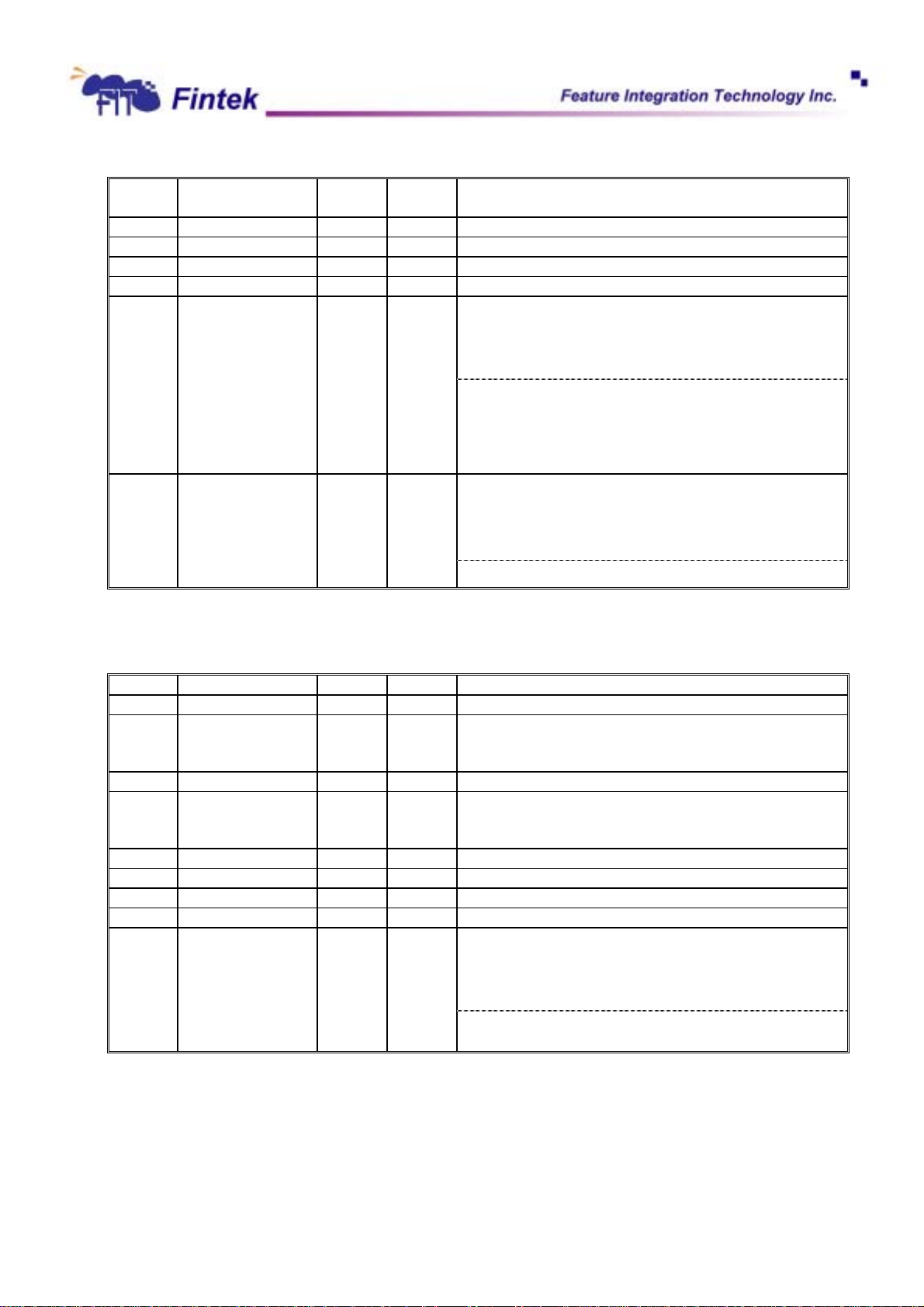
5.6 H/W Monitor
Pin No. Pin Name Type PWR Description
91-98 VIN8~VIN1 AIN VCC Voltage input 8 ~ 1.
73-75 FAN_TAC1~
FAN_TAC3
IN
ts
VCC Fan tachometer inputs.
9
Dec., 2006
V0.25P
Page 12
F71805
78-80 FAN_CTL1~
FAN_CTL3
87-89 D3~ D1 AIN VCC CPU thermal diode/transistor temperature sensor input.
90 VREF AOUT
81 PME# OD12 VCC Generated PME event.
85 OVT# OD12 VCC Generated over temperature event.
49-52 GP00~ GP03/
Voltage_fault1~4
O12 VCC Fan control outputs. These pins provide PWM duty-cycle
output or a voltage output.
VCC Voltage sensor output.
I/OOD
VCC
12t
General purpose IO.
1. Support Level and Pulse mode output.
2. Open drain and drive select.
3. Without input de-bounce.
Voltage fault indication for VIN abnormal event.
VIN1 Æ Voltage_fault1
VIN2 Æ Voltage_fault2
VIN3 Æ Voltage_fault3
VIN4 Æ Voltage_fault4
53-55 GP04~ GP06/
VIN7_ID0~2
I/OOD
VCC
12t
General purpose IO.
1. Support Level and Pulse mode output.
2. Open drain and drive select
3. Without input de-bounce.
Voltage fault indication is for VIN7 abnormal event ID.
5.7 Flash ROM Interface and GPIO
Pin No. Pin Name Type PWR Description
7-14 FD0~ FD7 I/O8t VCC Flash ROM interface data [0:7].
16-23 FA0~ FA7/
GP10~ GP17
24-25 FA8~ FA9 O8 VCC Flash ROM interface address [8:9].
26-33 FA10~ FA17/
GP20~ GP27
34 FRD# O8 VCC Flash ROM interface Read Strobe#.
47 FCS# O8 VCC Flash ROM interface Chip Select#.
48 FWE# O8 VCC Flash ROM interface Write Enable#.
59 FA18 O8 VCC Flash ROM interface address18.
56 GP07/FANCTL I/OOD
O8
I/O
O8
I/O
8t
8t
VCC The first functions of these pins are the Flash ROM interface
address [0:7].
The second Functions of these pins are GPIO [10:17].
VCC The first functions of these pins are the Flash ROM interface
address [10:17].
The second Functions of these pins are GPIO [20:27].
VCC
12t
General purpose IO.
1. Support Level and Pulse mode output.
2. Open drain and drive select
3. Without input de-bounce.
Fan 1 control output for Intel 4-pin Fan. All the registers are
as same as FANCTL1.
10
Dec., 2006
V0.25P
Page 13
6. Function Description
6.1 Power on Strapping Options
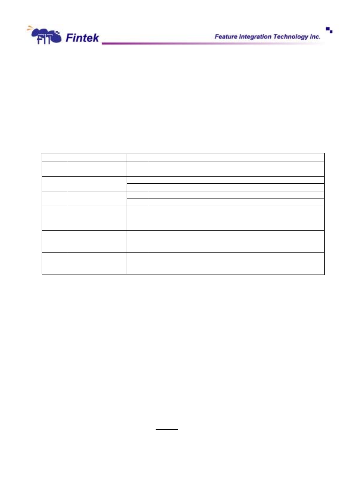
The F71805 provides four pins for power on hardware strapping to select functions. There is a form
to describe how to set the functions you want.
Pin No. Symbol Value Description
121 JP1
122 JP2
124 JP3
F71805
1 Fan control mode: PWM mode. ( Default) 1 JP4
0 Fan control mode: Linear mode.
1 ISA ROM Interface enable ( Default) 2 JP6
0 Reserved
1 Chip selection in configuration 4E. (Default) 5 JP5
0 Chip selection in configuration 2E.
1 Flash Rom Interface Address Segment 1 Enable (Default)
(FFFC0000h-FFFFFFFFh, 000E0000h-000FFFFFh).
0 Disable.
1 Flash Rom Interface Address Segment 2 Enable (Default)
(FFEE0000h-FFEFFFFFh).
0 Disable.
1 Flash Rom Interface Address Segment 3 Enable (Default)
(FFF80000h-FFFBFFFFh).
0 Disable.
6.2 Hardware Monitor
6.2.1 Analog Input
The F71805 provides 8 pins (8-bit) ADC voltage inputs. These input voltages should be positive and is
limited at range of 0v to 2.048V. The minimum resolution (1-LSB) is 8mV. If the voltage is over this range,
the divider resistor must be added and the divided voltage is also in the range of 0V to 2.048V.
The maximum input voltage of the analog pin is 2.048V because the 8-bit ADC has a 8mv LSB. Really,
the application of the PC monitoring would most often be connected to power suppliers. The voltage range
of 0V to 2.048V can be connected to these analog inputs. The 3.3V and VSB5V should be reduced a factor
with external resistors so as to obtain the input range..
There are 8 voltage inputs in the F71805 and the voltage divided formula is shown as follows:
R
2
If we choose R1=27K, R2=5.1K, the exact input voltage for V+12v will be 1.907V, which is within the
×=
VVIN
V
+
12
RR
+
21
For instance, where V
is the analog input voltage.
+12V
11
Dec., 2006
V0.25P
Page 14
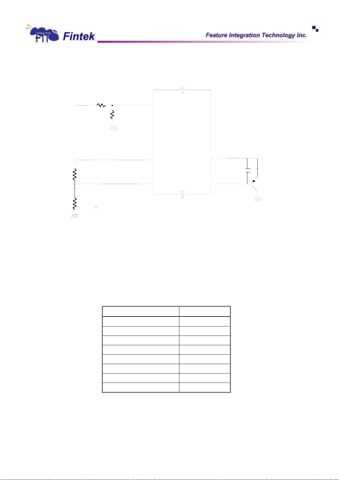
tolerance. As for application circuit, it can be refer to the figure shown as follows.
VIN(Lower than 2.048V)
R1
R2
F71805
F71805
VREF
R
10K, 1%
Typical Thermister
Connection
10K, 25 C
D1/D2/D3
D1/D2/D3
AGND(D-)
C
2200pF
2N3906
6.2.2 Temperature Monitoring and Offset
The F71805 can be measured from 0°C to 140°C. The status depends on different situation. As
connected to a BJT thermal diode, detected temperature ranges from 0°C to 140°C without considering
the OFFSET effect. As connected to a thermistor, detected temperature ranges from 0°C to 127°C without
considering the OFFSET effect. The temperature format is as the following table:
Temperature ( High Byte ) Digital Output
0°C 0000 0000
1°C 0000 0001
25°C 0001 1001
50°C 0011 0010
75°C 0100 1011
90°C 0101 1010
100°C 0110 0100
140°C 1000 1100
The F71805 provides offset register for each temperature. The offset value is an 7-bit, 2’s
complement value. The reading temperature value will be the result of the offset value added to the
monitored value. The offset format is as the following table:
12
Dec., 2006
V0.25P
Page 15
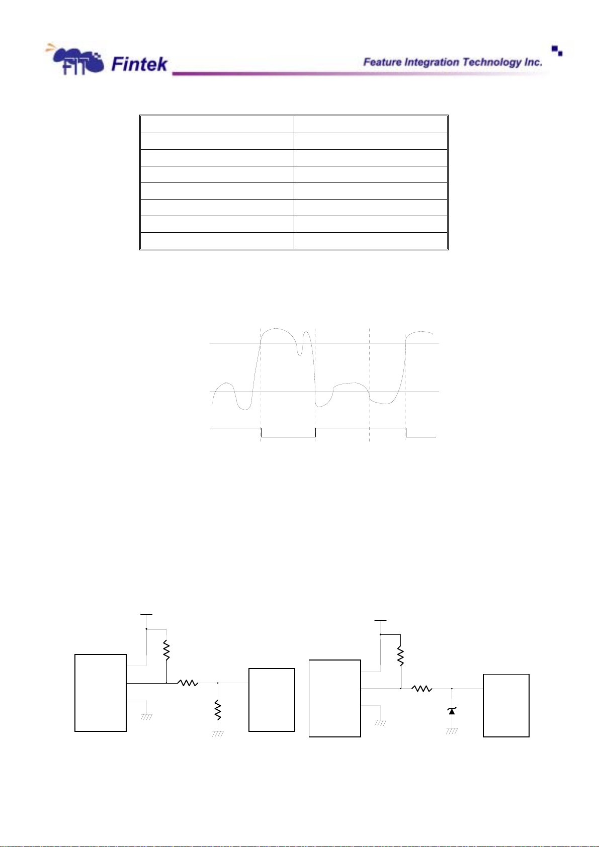
The F71805 can provide two external thermal sensors to detect temperature. When monitored
temperature exceeds the over-temperature threshold value, OVT# (pin85) will be asserted until the
temperature goes below the hysteresis temperature.
F71805
Offset Value High Byte
63°C 0011 1111
2°C 0000 0010
1°C 0000 0001
0°C 0000 0000
-1°C 0100 0001
-2°C 0100 0010
-64°C 0100 0000
To
T
HYST
OVT#
6.2.3 Fan speed count
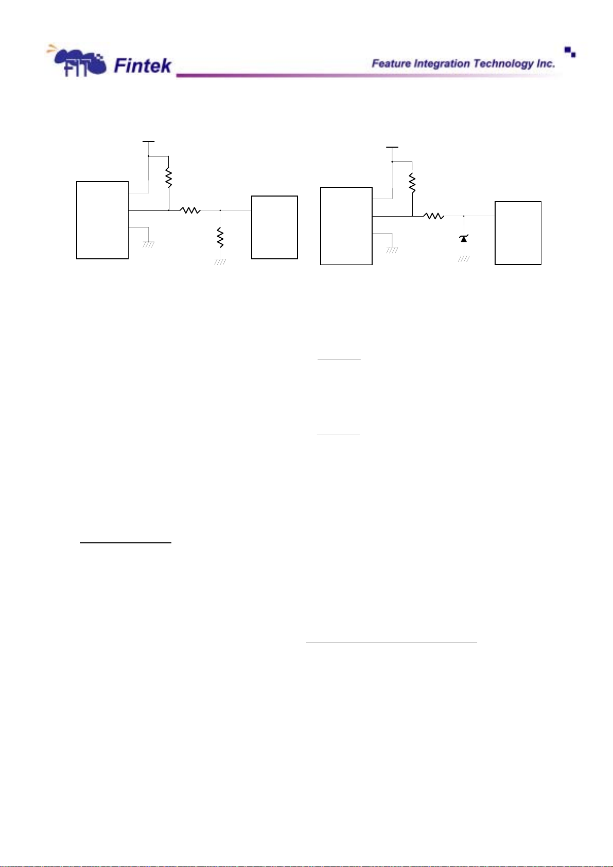
Inputs are provided by the signals from fans equipped with tachometer outputs. The level of these
signals should be set to TTL level, and maximum input voltage cannot be over VCC. If the input signals
from the tachometer outputs are over the VCC, the external trimming circuit should be added to reduce
the voltage to obtain the input specification. The normal circuit and trimming circuits are shown as follows:
+12V
FAN Out
GND
+12V
Pull-up resister
4.7K Ohms
22K~30K
Fan Input
10K
FANIN 1
F71805
FAN
Connector
+12V
FAN Out
GND
+12V
Pull-up resister < 1K
or totem-pole output
> 1K
3.3V Zener
Fan Input
FANIN 1
F71805
Fan with Tach Pull-Up to +12V, or Totern-Pole
Output and Register Attenuator
13
Fan with Tach Pull-Up to +12V, or
Totem-Pole Putput and Zener Clamp
Dec., 2006
V0.25P
Page 16
FAN Out
+5V
GND
+5V
Pull-up resister
4.7K Ohms
1K~2.7K
Fan Input
10K
FANIN1
F71805
FAN Out
FAN
Connector
+5V
GND
+5V
Pull-up resister < 1K
or totem-pole output
> 1K
3.3V Zener
F71805
Fan Input
FANIN1
F71805
Fan with Tach Pull-Up to +5V, or Totern-Pole
Output and Register Attenuator
Fan with Tach Pull-Up to +5V, or
Totem-Pole Putput and Zener Clamp
Determine the fan counter according to:
6
105.1 ×
RPM
Count
=
In other words, the fan speed counter has been read from register, the fan speed can be evaluated by the
following equation. As for fan, it would be best to use 2 pulses tachmeter output per round.
6
RPM
=
105.1 ×
Count
6.2.4 Fan speed control
The F71805 provides 2 fan speed control methods: 1. Linear FAN Control 2. PWM Duty Cycle
Linear Fan Control
The range of DC output is 0~3.3V, controlled by 8-bit register (CR6Bh for FAN1, CR7Bh for FAN2
and CR8Bh for FAN3). 1 LSB is about 0.013V. The output DC voltage is amplified by external OP circuit,
thus to reach maximum FAN OPERATION VOLTAGE, 12V.
The output voltage will be given as followed:
And the suggested application circuit for linear fac control would be:
3.3(V) tageOutput_vol ×=
ValueRegister bit -8 Programmed
255
14
Dec., 2006
V0.25P
Page 17
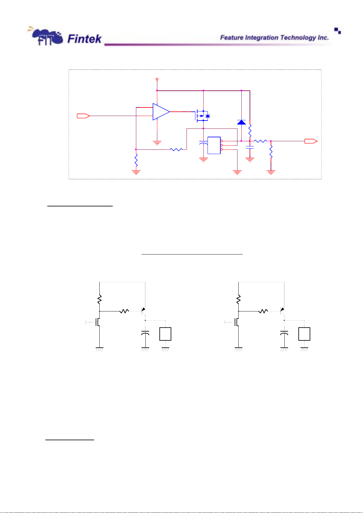
DC OUTPUT VOLTAGE
3.9K
F71805
12V
84
3
+
2
-
LM358
R
PMOS
1
JP1
R10K
DC FAN Control with OP
C
47u
CON3
1N4148
3
2
1
D1
C
0.1u
R
4.7K
R27K
R
10K
FANIN MONITOR
PWM duty Fan Control
The duty cycle of PWM can be programmed by a 8-bit register which are defined in the CR6Bh,
CR7Bh and CR8Bh. The default duty cycle is set to 100%, that is, the default 8-bit registers is set to FFh.
The expression of duty can be represented as follows.
(%)Duty_cycle ×=
ValueRegister bit -8 Programmed
%100
255
R1
D
NMOS
S
+5V
R2
PNP Transistor
+
C
-
FAN
PWM Clock Input
+12V
R1
R2
D
G
NMOS
S
PNP Transistor
+
C
-
FAN
PWM Clock Input
G
6.2.5 Fan speed control mechanism
There are 3 modes to control fan speed and they are manual, fan speed mode and temperature
mode. For manual mode, it generally acts as PWM fan speed control. As for speed mode and
temperature mode, they are more intelligent fan speed control and described as below:
Fan Speed mode
Fan speed mode is an intelligent method according to expected fan speed pre-setting by BIOS. In the
beginning, fan speed will be operated at full speed and the F71805 will get the full speed count value.
After that, the fan speed will automatically rotate according to the expected fan speed setting by BIOS.
15
Dec., 2006
V0.25P
Page 18
r
For instance, the register CR69h and CR6Ah are used for this mode of FAN1.
Temperature mode
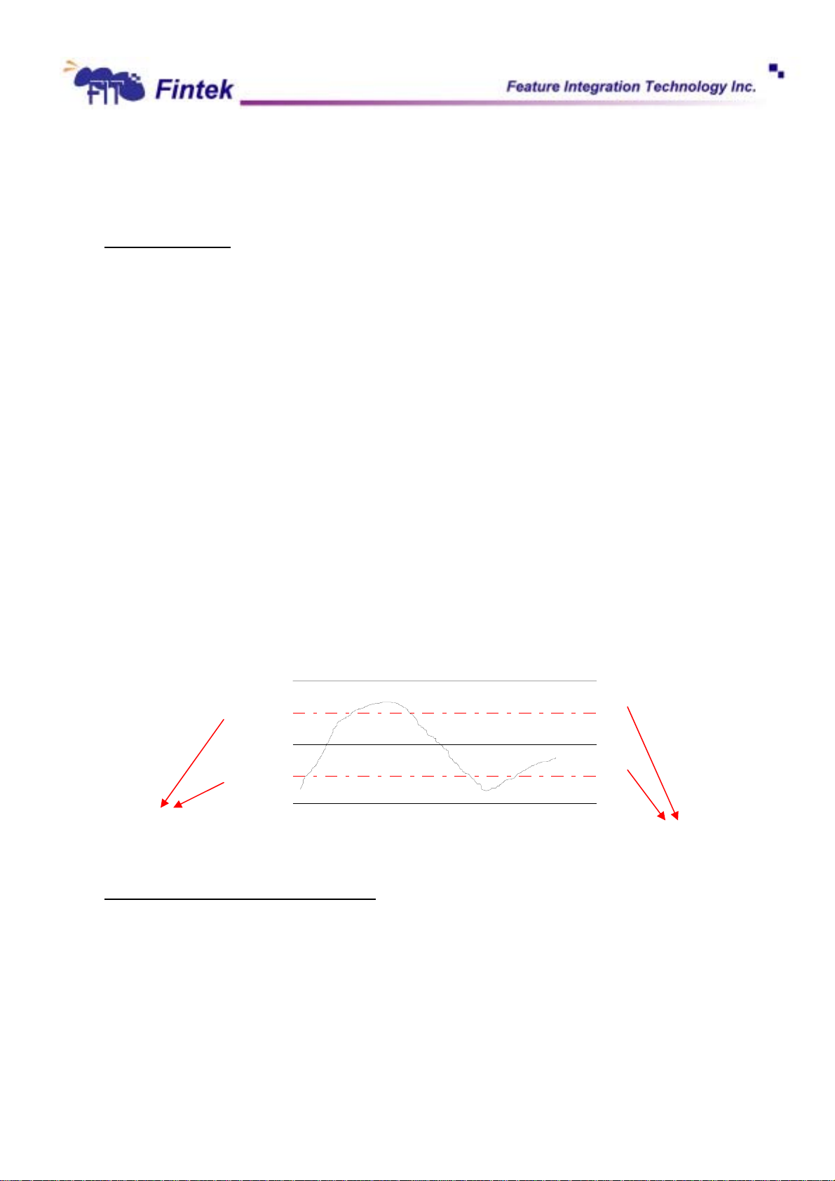
At this mode, F71805 provides the clever system to automatically control fan speed related to
temperature system. The F71805 can provide three temperature boundaries and three intervals for user
setting, and each interval has its related fan speed count. All these values should be set by BIOS first. In
the F71805 design, the F71805 will auto-generate temperature boundaries (average value) between
those boundaries that user setting, and it will auto-produce interval fan speed count (average value)
between users setting value.
If the temperature value is set to 40, 50 and 90°C, it will auto-generate two temperature boundaries
F71805
value of 45°C (This value is calculated automatically by hardware design of the F71805. (50+40)/2 =45 )
and 70°C. The same way, the related desired fan speed counts for each interval are 4200RPM, 3600RPM,
3000RPM, 2500RPM, 2000RPM and Stop Counts. When the temperature is within 50~70°C, the fan
speed counts will be 3000RPM (Registers CRA4h~CRA9h, CRB4h~CRB9h and CRC4h~CRC9h). The
F71805 will auto-adjust PWMOUT (PWM_DUTY) to make fan speed match the expected value. It can be
said that the fan will be turned on with a specific speed set by BIOS and automatically controlled with the
temperature varying. The F71805 will take charge of all the fan speed control and need no software
support.
Auto-Generated
(Average value)
90 Degree C
70 Degree C
50 Degree C
45 Degree C
40 Degree C
Desired Counts (RPM)
4200
3600
3000
2500
2000
Stop Counts
Auto-Gene
(Average value)
ated
PWMOUT Duty-cycle operating process
In both “FAN SPEED” and “TEMPERATURE” modes, F71805 adjust PWMOUT (PWM_DUTY1
(CR6B) of Fan1, PWM_DUTY2 (CR7B) of Fan2, PWM_DUTY3 (CR8B) of Fan3) duty-cycle according to
current fan count and expected fan count. It will operate as follows:
(1). When expected count is FFFFh, PWMOUT duty-cycle (PWM_DUTY)will be set to 00h to turn off
fan.
(2). When expected count is 0000h, PWMOUT duty-cycle (PWM_DUTY) will be set to FFh to turn on
fan with full speed.
16
Dec., 2006
V0.25P
Page 19
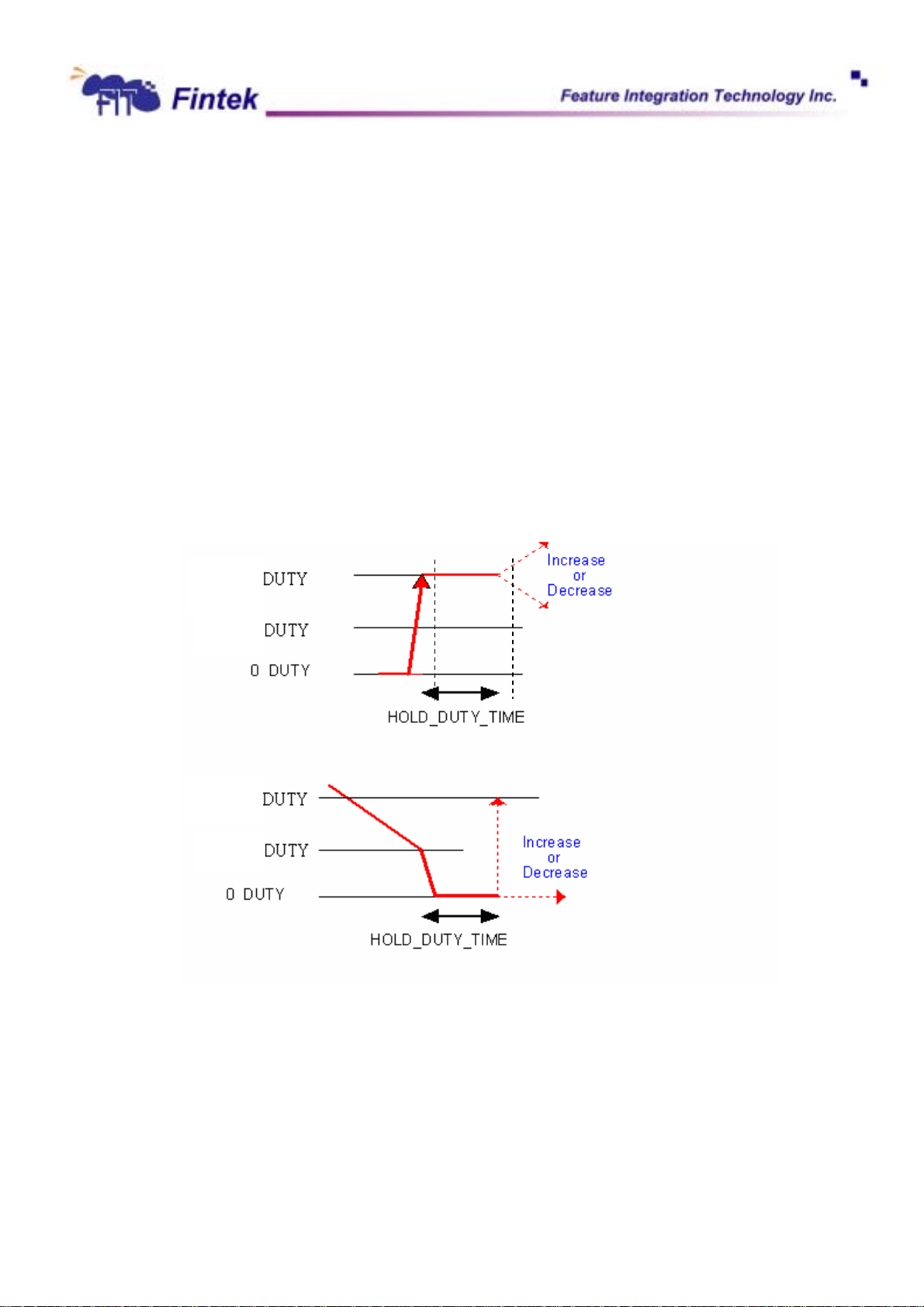
(3). If both (1) and (2) are not true and KEEP_STOP (see INDEX 60h) is set to 0:
F71805
(a). When PWMOUT duty-cycle decrease to STOP_DUTY(≠ 00h), obviously the duty-cycle will
decrease to 00h next, F71805 will keep duty-cycle at 00h 3 seconds
starts to compare current fan count and expected count in order to increase or decrease its
duty-cycle. This ensures that if there is any glitch during the 3 seconds
ignore it.
(b). When PWMOUT duty-cycle increase from 00h to START_DUTY(≠ 00h), F71805 also will
keep duty-cycle at START_DUTY 3 seconds
1
. After that, F71805 starts to compare current
fan count and expected count in order to increase or decrease its duty-cycle. This ensures
that if there is any glitch during the 3 seconds
1
period, F71805 will ignore it.
1
. After that, F71805
1
period, F71805 will
Note 1: The period of HOLD_DUTY_TIME can be programmed at INDEX 67h of FAN1.
START
STOP
START
STOP
6.2.6 FAN_FAULT#
Fan_Fault will be asserted ( PME# Pin 81) when the fan speed doesn’t meet the expected fan speed
within a programmable period (default is 3 seconds) or when PWMOUT duty-cycle is 100%.
17
Dec., 2006
V0.25P
Page 20

)
F71805
Current Fan Count
Expected Fan Count
100%
Duty-cycle
Fan_Fault#
3 sec(default
6.2.7 VOLT_FAULT# (Voltage Fault Signal)
When voltage leaps from the security range setting by BIOS, the warning signal VOLT_FAULT# will
be activated. Shown in figure.
High limit
Low limit
VOLT_FAULT#
6.3 FDC
The Floppy Disk Controller provides the interface between a host processor and one floppy disk
drives. It integrates a controller and a digital data separator with write pre-compensation, data rate
selection logic, microprocessor interface, and a set of registers. The FDC supports data transfer rates of
250 Kbps, 300 Kbps, 500 Kbps, and 1 Mbps. It operates in PC/AT mode and supports 3-mode type drives.
The FDC configuration is handled by software and a set of Configuration registers. Status, Data, and
Control registers facilitate the interface between the host microprocessor and the disk drive, providing
information about the condition and/or state of the FDC. These configuration registers can select the data
rate, enable interrupts, drives, and DMA modes, and indicate errors in the data or operation of the
FDC/FDD. The controller manages data transfers using a set of data transfer and control commands.
These commands are handled in three phases: Command, Execution, and Result. Not all commands
utilize all these three phases.
18
Dec., 2006
V0.25P
Page 21

6.4 UART
The UARTs are used to convert data between parallel format and serial format. They convert parallel
data into serial format on transmission and serial format into parallel data on receiver side. The serial
format is formed by one start bit, followed by five to eight data bits, a parity bit if programmed and one
( 1.5 or 2 ) stop bits. The UARTs include complete modem control capability and an interrupt system that
may be software trailed to the computing time required to handle the communication link. They have FIFO
mode to reduce the number of interrupts presented to the host. Both receiver and transmitter have a
16-byte FIFO.
F71805
6.5 Parallel Port
The parallel port in F71805 supports an IBM XT/AT compatible parallel port ( SPP ), bi-directional
paralle port ( BPP ), Enhanced Parallel Port ( EPP ), Extended Capabilities Parallel Port ( ECP ) mode.
Refer to the configuration registers for more information on selecting the mode of operation.
7. Register Description
7.1 Global Control Registers
The configuration register is used to control the behavior of the corresponding devices. To configure
the register, using the index port to select the index and then writing data port to alter the parameters. The
default index port and data port are 0x4E and 0x4F respectively. Pull down the SOUT2/JP5 pin to change
the default value to 0x2E/0x2F. To enable configuration, the entry key 0x87 must be written to the index
port. To disable configuration, write exit key 0xAA to the index port. Following is a example to enable
configuration and disable configuration by using debug.
-o 4e 87
-o 4e 87 ( enable configuration )
-o 4e aa ( disable configuration )
19
Dec., 2006
V0.25P
Page 22
7.1.1 Software Reset Register Index 02h
Bit Name R/W Default Description
7-1 Reserved - - Reserved.
0 SOFT_RST R/W 0 Write 1 to reset the register and device powered by VDD ( VCC ).
7.1.2 Logic Device Number Register Index 07h
Bit Name R/W Default Description
7-0 LDN R/W 00h 00h: Select FDC device configuration registers.
F71805
01h: Select UART 1 device configuration registers.
02h: Select UART 2 device configuration registers.
03h: Select Parallel Port device configuration registers.
04h: Select Hardware Monitor device configuration registers.
06h: Select GPIO device configuration registers.
0ah: Select PME device configuration registers.
Otherwise: reserved.
7.1.3 Chip ID Register Index 20h
Bit Name R/W Default Description
7-0 CHIP_ID1 R 04h Chip ID 1 of F71805.
7.1.4 Chip ID Register Index 21h
Bit Name R/W Default Description
7-0 CHIP_ID2 R 06h Chip ID2 of F71805.
7.1.5 Vendor ID Register Index 23h
Bit Name R/W Default Description
7-0 VENDOR_ID1 R 19h Vendor ID 1 of Fintek devices.
7.1.6 Vendor ID Register Index 24h
Bit Name R/W Default Description
7-0 VENDOR_ID2 R 34h Vendor ID 2 of Fintek devices.
7.1.7 Software Power Down Register Index 25h
Bit Name R/W Default Description
20
Dec., 2006
V0.25P
Page 23
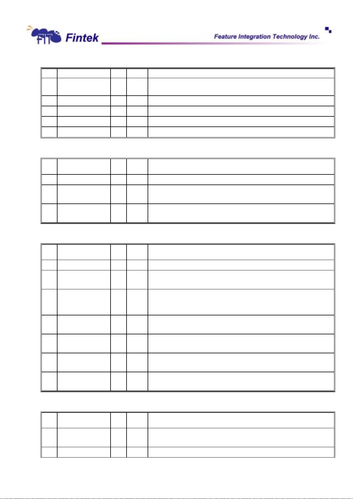
7-6 Reserved - - Reserved
4 SOFTPD_HM R/W 0
3 SOFTPD_PRT R/W 0
2 SOFTPD_UR2 R/W 0
1 SOFTPD_UR1 R/W 0
0 SOFTPD_FDC R/W 0
7.1.8 UART IRQ Sharing Register Index 26h
Bit Name R/W Default Description
F71805
Power down the Hardware Monitor device. This will stop the Hardware Monitor
clock.
Power down the Parallel Port device. This will stop the Parallel Port clock.
Power down the UART 2 device. This will stop the UART 2 clock.
Power down the UART 1 device. This will stop the UART 1 clock.
Power down the FDC device. This will stop the FDC clock.
7-2 Reserved - -
1 IRQ_MODE R/W 0
0 IRQ_SHAR R/W 0
Reserved.
0: PCI IRQ sharing mode (low level).
1: ISA IRQ sharing mode (low pulse).
0: disable IRQ sharing of two UART devices.
1: enable IRQ sharing of two UART devices.
7.1.9 Power On Trap Status Register Index 27h
Bit Name R/W Default Description
7-6 Reserved - -
5 PORT4E_EN R/W 1
4 XBUS_EN R/W 1
3 SEG_000E_EN R/W 1
2 SEG_FFFF_EN R/W 1
1 SEG_FFEF_EN R/W 1
0 SEG_FFF8_EN R/W 1
Reserved.
0: Configuration Register port is 2E/2F.
1: Configuration Register port is 4E/4F.
0: disable XBUS. FA17/GP27 ~ FA10/GP20 function as GP2. FA7/GP17 ~
FA0/GP10 function as GP1.
1: enable XBUS.
0: disable segment 000E0000h-000EFFFFh.
1: enable segment 000E000h-000EFFFFh.
0: disable segment FFFFFFFFh-FFFC0000h.
1: enable segment FFFFFFFFh-FFFC0000h.
0: disable segment FFEFFFFFh-FFEE0000h.
1: enable segment FFEFFFFFh-FFEE0000h.
0: disable segment FFFBFFFFh-FFF80000h.
1: enable segment FFFBFFFFh-FFF80000h.
7.1.10 Flash Control Register Index 28h
Bit Name R/W Default Description
7 FLASH_WR_EN R/W 0
6-5 Reserved - -
0: disable flash write.
1: enable flash write.
Reserved.
21
Dec., 2006
V0.25P
Page 24
F71805
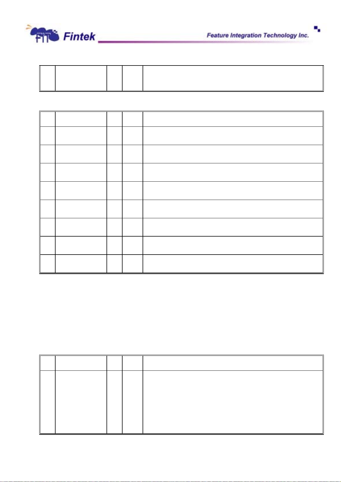
4-0 WAIT_TIMES R/W 8h
Adjust the cycles of the FCS# to improve the performance of the XBUS.
The length of FCS# is from 7 LCLK cycles ( WAIT_TIMES == 00h) to 38 LCLK
cycles (WAIT_TIMES == 1fh).
7.1.11 Voltage Fault Enable Register Index 29h
Bit Name R/W Default Description
7
FANCTL_GPEN R/W 0
6 VIN7_ID2_EN R/W 0
5 VIN7_ID1_EN R/W 0
4 VIN7_ID0_EN R/W 0
3 VOLT_FAULT4_EN R/W 0
2 VOLT_FAULT3_EN R/W 0
1 VOLT_FAULT2_EN R/W 0
0 VOLT_FAULT1_EN R/W 0
0: the function of GP07 is GP07.
1: the function of GP07 is FANCTL.
0: the function of GP06/VIN7_ID2 is GP06.
1: the function of GP06/VIN7_ID2 is VIN7_ID2.
0: the function of GP05/VIN7_ID1 is GP05.
1: the function of GP05/VIN7_ID1 is VIN7_ID1.
0: the function of GP04/VIN7_ID0 is GP04.
1: the function of GP04/VIN7_ID0 is VIN7_ID0.
0: the function of GP03/Voltage_fault4 is GP03.
1: the function of GP03/Voltage_fault4 is Voltage_fault4.
0: the function of GP02/Voltage_fault3 is GP02.
1: the function of GP02/Voltage_fault3 is Voltage_fault3.
0: the function of GP01/Voltage_fault2 is GP01.
1: the function of GP01/Voltage_fault2 is Voltage_fault2.
0: the function of GP00/Voltage_fault1 is GP00.
1: the function of GP00/Voltage_fault1 is Voltage_fault1.
7.2 FDC Register
7.2.1 Logic Device Number Register
Logic Device Number Register
Bit Name R/W Default Description
7-0 LDN R/W 00h 00h: Select FDC device configuration registers.
Index 07h
01h: Select UART 1 device configuration registers.
02h: Select UART 2 device configuration registers.
03h: Select Parallel Port device configuration registers.
04h: Select Hardware Monitor device configuration registers.
06h: Select GPIO device configuration registers.
0ah: Select PME device configuration registers.
Otherwise: reserved.
22
Dec., 2006
V0.25P
Page 25
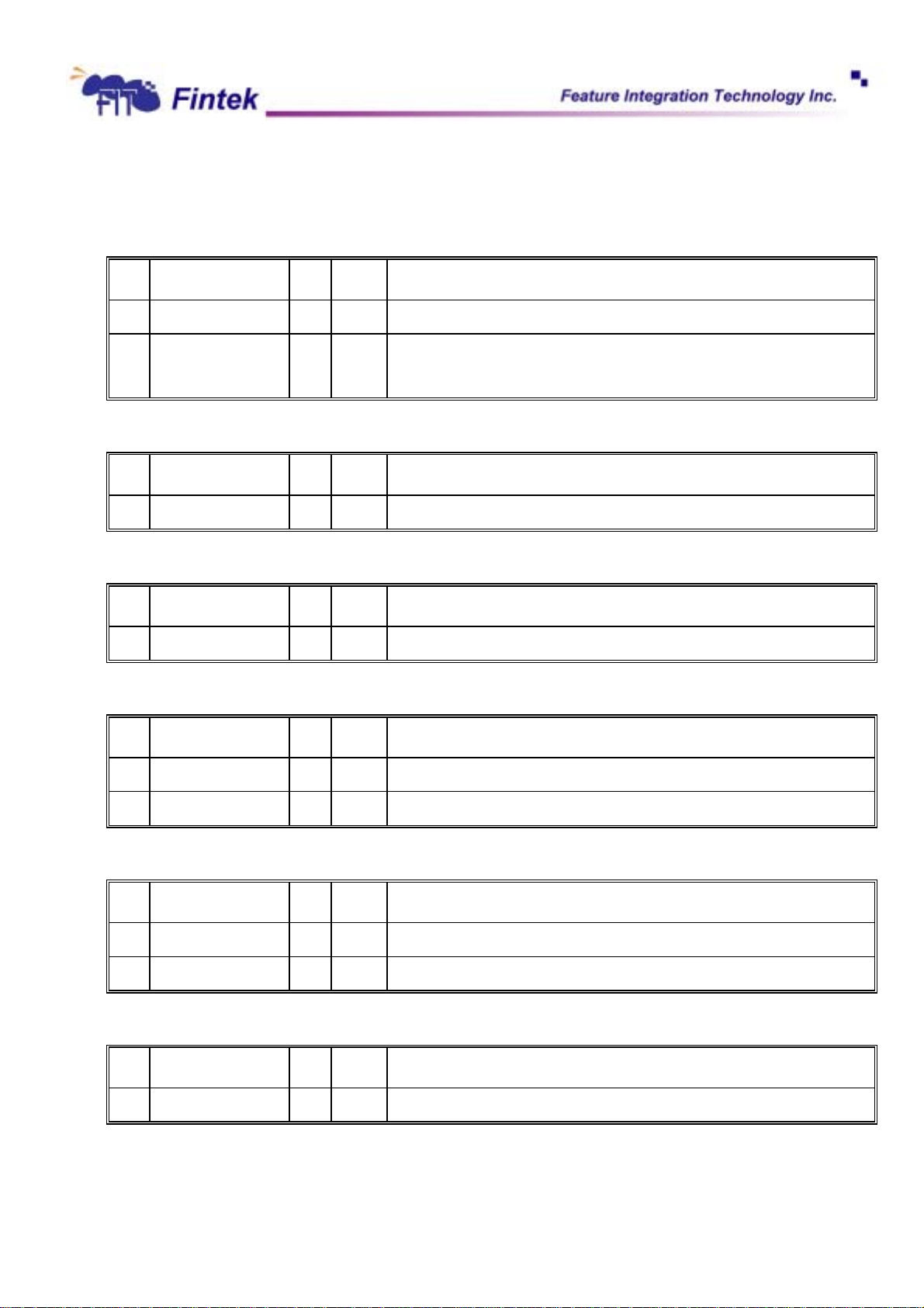
7.2.2 FDC Configuration Registers
FDC Device Enable Register Index 30h
Bit Name R/W Default Description
7-1 Reserved - - Reserved
0 FDC_EN R/W 1 0: disable FDC.
Base Address High Register Index 60h
Bit Name R/W Default Description
F71805
1: enable FDC.
7-0 BASE_ADDR_HI R/W 03h The MSB of FDC base address.
Base Address Low Register Index 61h
Bit Name R/W Default Description
7-0 BASE_ADDR_LO R/W F0h The LSB of FDC base address.
IRQ Channel Select Register Index 70h
Bit Name R/W Default Description
7-4 Reserved - - Reserved.
3-0 SELFDCIRQ R/W 06h Select the IRQ channel for FDC.
DMA Channel Select Register Index 74h
Bit Name R/W Default Description
7-3 Reserved - - Reserved.
2-0 SELFDCDMA R/W 010 Select the DAM channel for FDC.
FDD Mode Register Index F0h
Bit Name R/W Default Description
7-4 Reserved - - Reserved.
23
Dec., 2006
V0.25P
Page 26
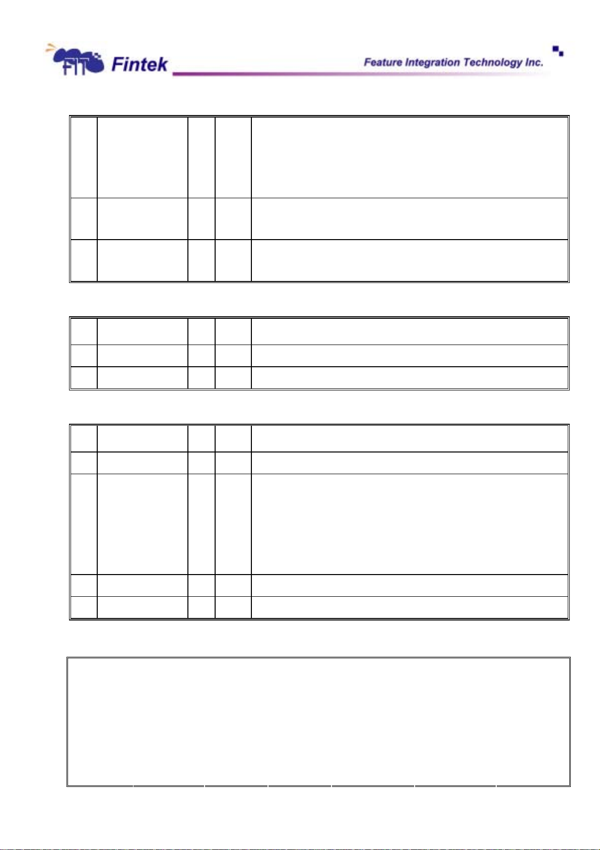
3-2 IF_MODE R/W 11 00: Model 30 mode.
1 FDMAMODE R/W 1 0: enable burst mode.
0 EN3MODE R/W 0 0: normal floppy mode (default).
FDD Drive Type Register Index F2h
F71805
01: PS/2 mode.
10: Reserved.
11: AT mode (default).
1: non-busrt mode (default).
1: enhanced 3-mode FDD.
Bit Name R/W Default Description
7-2 Reserved - - Reserved.
1-0 FDD_TYPE R/W 11 FDD drive type.
FDD Selection Register Index F4h
Bit Name R/W Default Description
7-5 Reserved - - Reserved.
4-3 FDD_DRT R/W 00 Data rate table select, refer to table A.
00: select regular drives and 2.88 format.
01: 3-mode drive.
10: 2 mega tape.
11: reserved.
2 Reserved - - Reserved.
1-0 FDD_DT R/W 00 Drive type select, refer to table B.
TABLE A
Data Rate Table Select Data Rate Selected Data Rate DENSEL
FDD_DRT[1] FDD_DRT[0] DATARATE1 DATARATE0 MFM FM
0 0 500K 250K 1
0 0
0 1 0 0 500K 250K 1
0 1 300K 150K 0
1 0 250K 125K 0
1 1 1Meg --- 1
24
Dec., 2006
V0.25P
Page 27
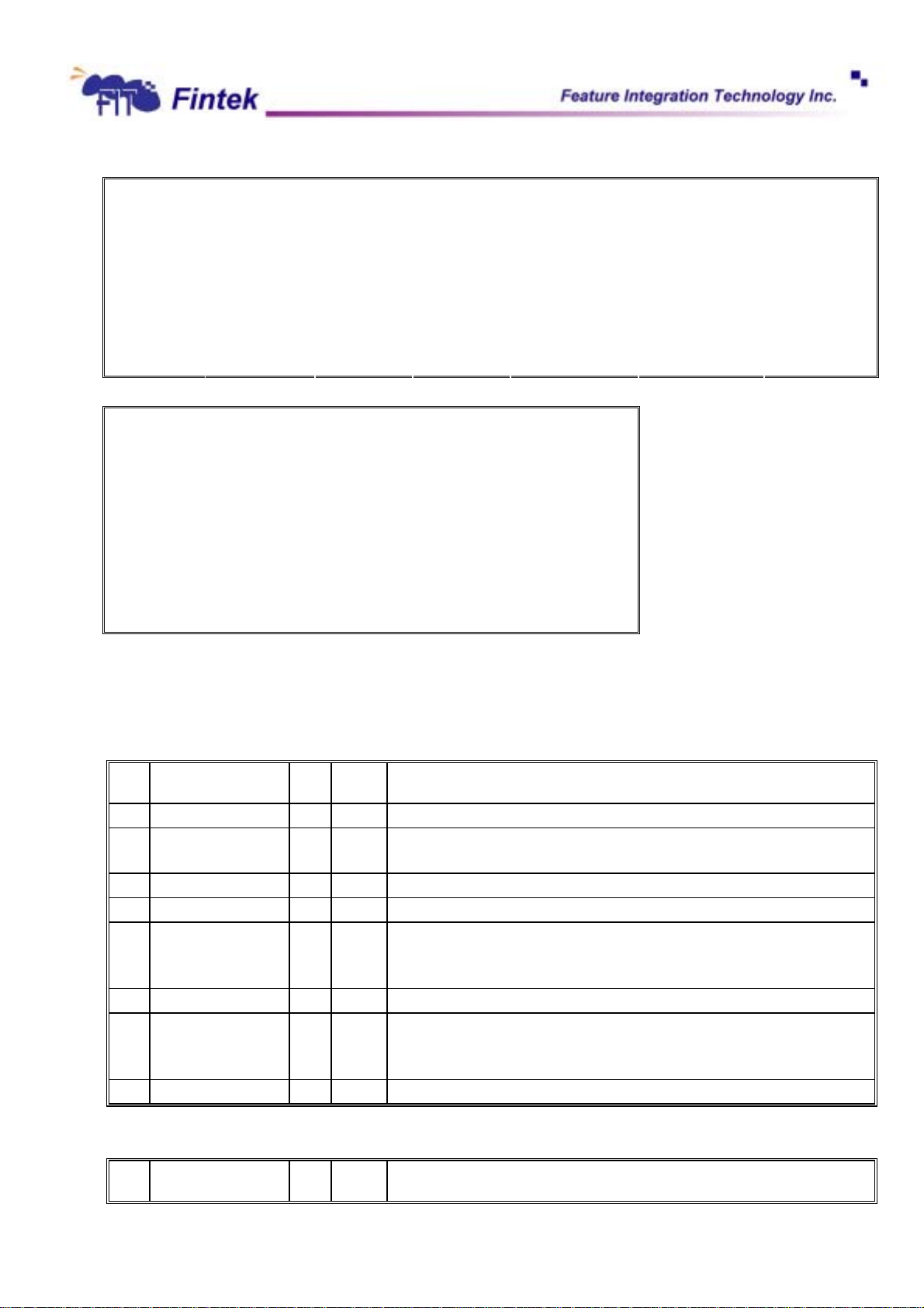
F71805
1 0
TABLE B
Drive Type
FDD_DT1 FDD_DT0
0 DENSEL 4/2/1 MB 3.5”
0
0 1 DATARATE1
1 0 DENSEL#
1 1 DATARATE0
0 1 500K 250K 0
1 0 250K 125K 0
1 1 1Meg --- 1
0 0 500K 250K 1
0 1 2Meg --- 0
1 0 250K 125K 0
1 1 1Meg --- 1
DRVDEN0 Remark
2/1 MB 5.25”
1/1.6/1 MB 3.5” (3-Mode )
7.2.3 Device Registers
7.2.3.1 Status Register A (PS/2 mode) Base + 0
Bit Name R/W Default Description
7 INTPEND R 0 This bit indicates the state of the interrupt output.
6 DRV2_N R - 0: a second drive has been installed.
1: a second drive has not been installed.
5 STEP R 0 This bit indicates the complement of STEP# disk interface output.
4 TRK0_N R - This bit indicates the state of TRK0# disk interface input.
3 HDSEL R 0 This bit indicates the complement of HDSEL# disk interface output.
0: side 0.
1: side 1.
2 INDEX_N R - This bit indicates the state of INDEX# disk interface input.
1 WPT_N R - This bit indicates the state of WPT# disk interface input.
0: disk is write-protected.
1: disk is not write-protected.
0 DIR R 0 This bit indicates the complement of DIR# disk interface output.
7.2.3.2 Status Register A (Model 30 mode) Base + 0
Bit Name R/W Default Description
25
Dec., 2006
V0.25P
Page 28
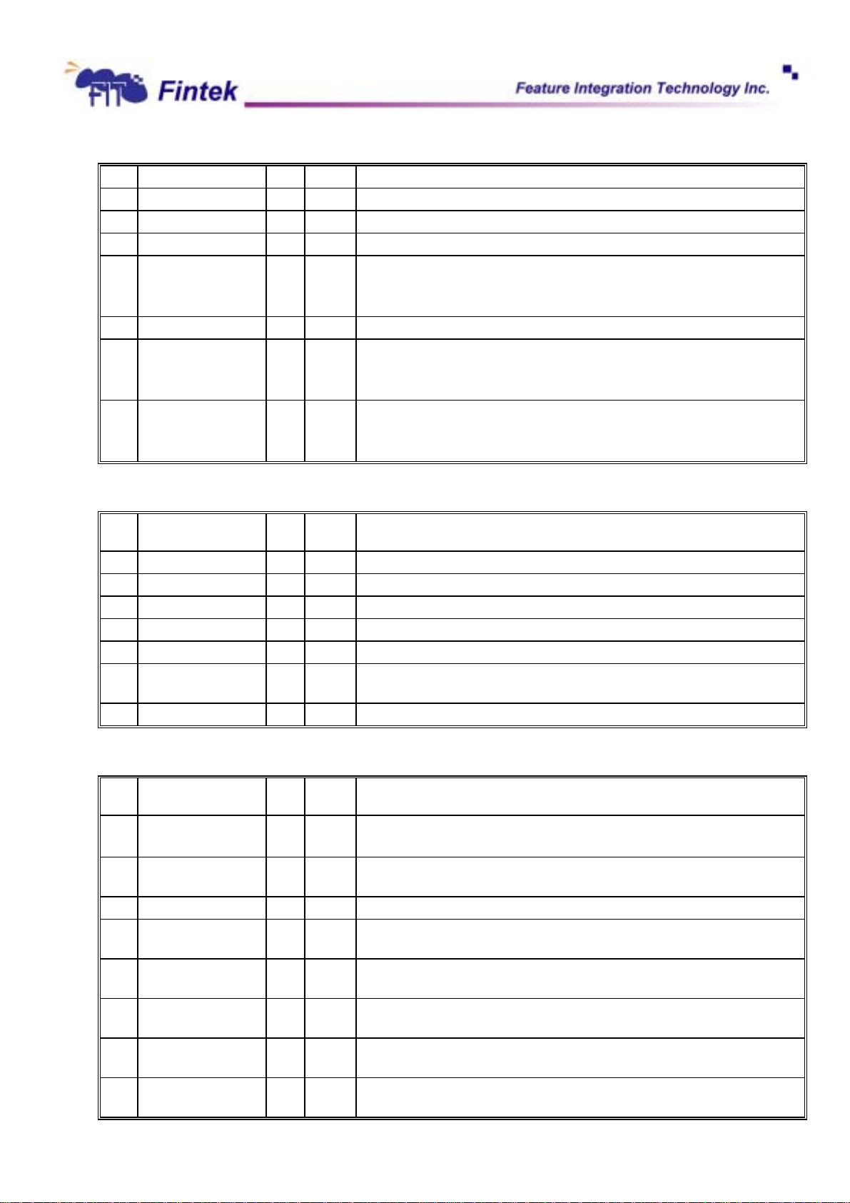
7 INTPEND R 0 This bit indicates the state of the interrupt output.
6 DRQ R 0 This bit indicates the state of the DRQ signal.
5 STEP_FF R 0 This bit indicates the complement of latched STEP# disk interface output.
4 TRK0 R - This bit indicates the complement of TRK0# disk interface input.
3 HDSEL_N R 1 This bit indicates the state of HDSEL# disk interface output.
2 INDEX R - This bit indicates the complement of INDEX# disk interface input.
1 WPT R - This bit indicates the complement of WPT# disk interface input.
0 DIR_N R 1 This bit indicates the state of DIR# disk interface output.
F71805
0: side 0.
1: side 1.
0: disk is write-protected.
1: disk is not write-protected.
0: head moves in inward direction.
1: head moves in outward direction.
7.2.3.3 Status Register B (PS/2 Mode) Base + 1
Bit Name R/W Default Description
7-6 Reserved R - Reserved. Return 11b when read.
5 DR0 R 0 Drive select 0. This bit reflects the bit 0 of Digital Output Register.
4 WDATA R 0 This bit changes state at every rising edge of WDATA#.
3 RDATA R 0 This bit changes state at every rising edge of RDATA#.
2 WGATE R 0 This bit indicates the complement of WGATE# disk interface output.
1 MOTEN1 R 0 This bit indicates the complement of MOB# disk interface output. Not support
in this design.
0 MOTEN0 R 0 This bit indicates the complement of MOA# disk interface output.
7.2.3.4 Status Register B (Model 30 Mode) Base + 1
Bit Name R/W Default Description
7 DRV2_N R - 0: a second drive has been installed.
1: a second drive has not been installed.
6 DSB_N R 1 This bit indicates the state of DRVB# disk interface output. Not support in this
design.
5 DSA_N R 1 This bit indicates the state of DRVA# disk interface output.
4 WDATA_FF R 0 This bit is latched at the rising edge of WDATA# and is cleared by a read from
the Digital Input Register.
3 RDATA_FF R 0 This bit is latched at the rising edge of RDATA# and is cleared by a read form
the Digital Input Register.
2 WGATE_FF R 0 This bit is latched at the falling edge of WGATE# and is cleared by a read from
the Digital Input Register.
1 DSD_N R 1 This bit indicates the complement of DRVD# disk interface output. Not support
in this design.
0 DSC_N R 1 This bit indicates the complement of DRVC# disk interface output. Not support
in this design.
26
Dec., 2006
V0.25P
Page 29
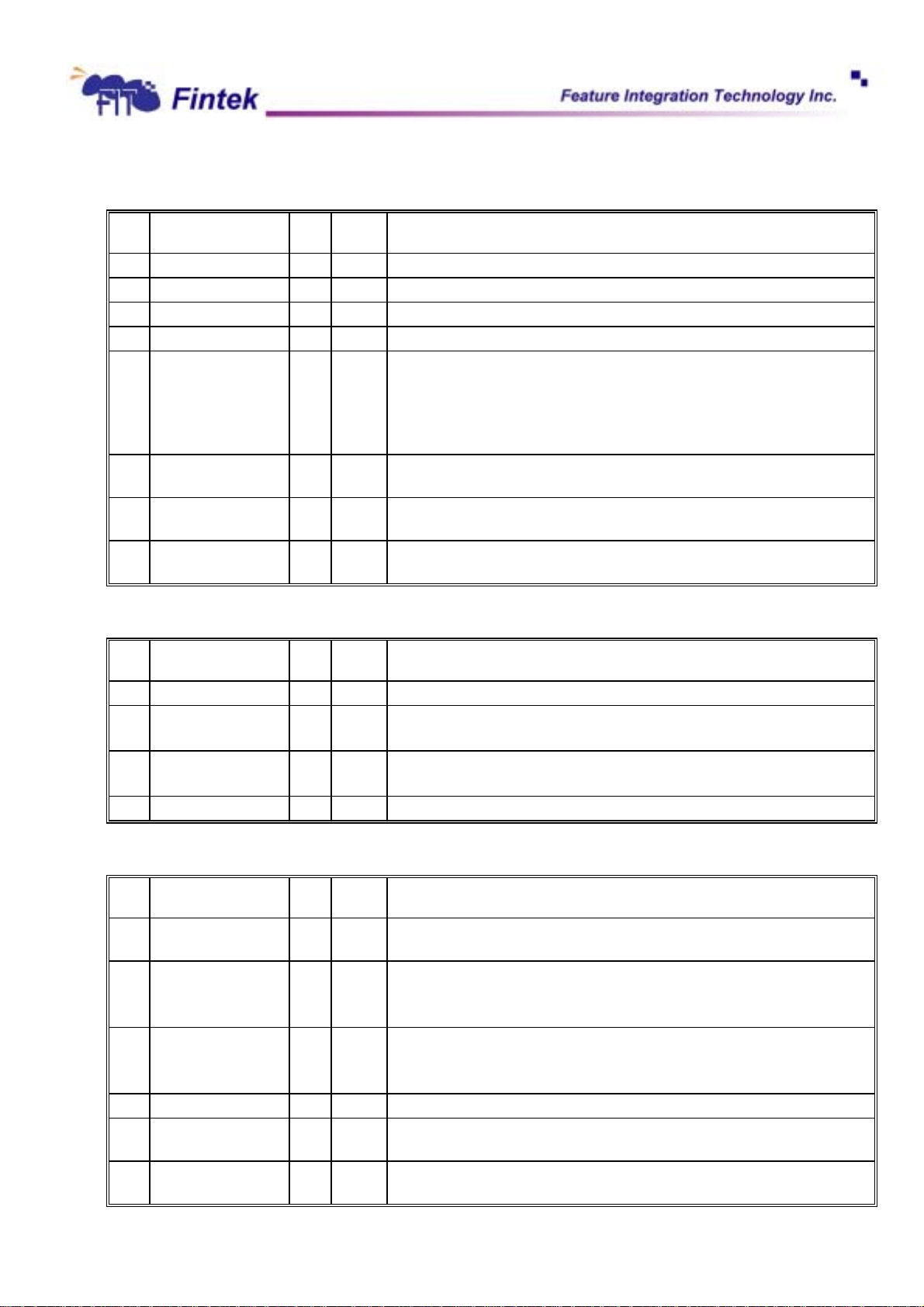
7.2.3.5 Digital Output Register Base + 2
Bit Name R/W Default Description
7 MOTEN3 R 0 Motor enable 3. Not support in this design.
6 MOTEN2 R 0 Motor enable 2. Not support in this design.
5 MOTEN1 R/W 0 Motor enable 1. Used to control MOB#. MOB# is not support in this design.
4 MOTEN0 R/W 0 Motor enable 0. Used to control MOA#.
3 DAMEN R/W 0 DMA enable. This bit has two mode of operation.
2 RESET R 0 Write 0 to this bit will reset the controller. I will remain in reset condition until a 1
1 DSD_N R 1 This bit indicates the complement of DRVD# disk interface output. Not support
0 DSC_N R 1 This bit indicates the complement of DRVC# disk interface output. Not support
F71805
PC-AT and Model 30 mode: write 1 will enable DMA and IRQ, write 0 will
disable DMA and IRQ.
PS/2 mode: This bit is reserved. DMA and IRQ are always enabled in PS/2
mode.
is written.
in this design.
in this design.
7.2.3.6 Tape Drive Register Base + 3
Bit Name R/W Default Description
7-6 Reserved R - Reserved. Return 00b when read.
5-4 TYPEID R 11 Reserved in normal function, return 11b when read.
If 3 mode FDD function is enabled. These bits indicate the drive type ID.
3-2 Reserved R 11 Reserved. Return 11b when read in normal function.
Return 00b when read in 3 mode FDD function.
1-0 TAPESEL R/W 00 These bits assign a logical drive number to be a tape drive.
7.2.3.7 Main Status Register Base + 4
Bit Name R/W Default Description
7 RQM R 0 Request for Master indicates that the controller is ready to send or receive data
from the uP through the FIFO.
6 DIO R 0 Data I/O (direction):
0: the controller is expecting a byte to be written to the Data Register.
1: the controller is expecting a byte to be read from the Data Register.
5 NON_DMA R 0 Non DMA Mode:
0: the controller is in DAM mode.
1: the controller is interrupt or software polling mode.
4 FDC_BUSY R 0 This bit indicate that a read or write command is in process.
3 DRV3_BUSY R 0 FDD number 3 is in seek or calibration condition. FDD number 3 is not support
in this design.
2 DRV2_BUSY R 0 FDD number 2 is in seek or calibration condition. FDD number 2 is not support
in this design.
27
Dec., 2006
V0.25P
Page 30
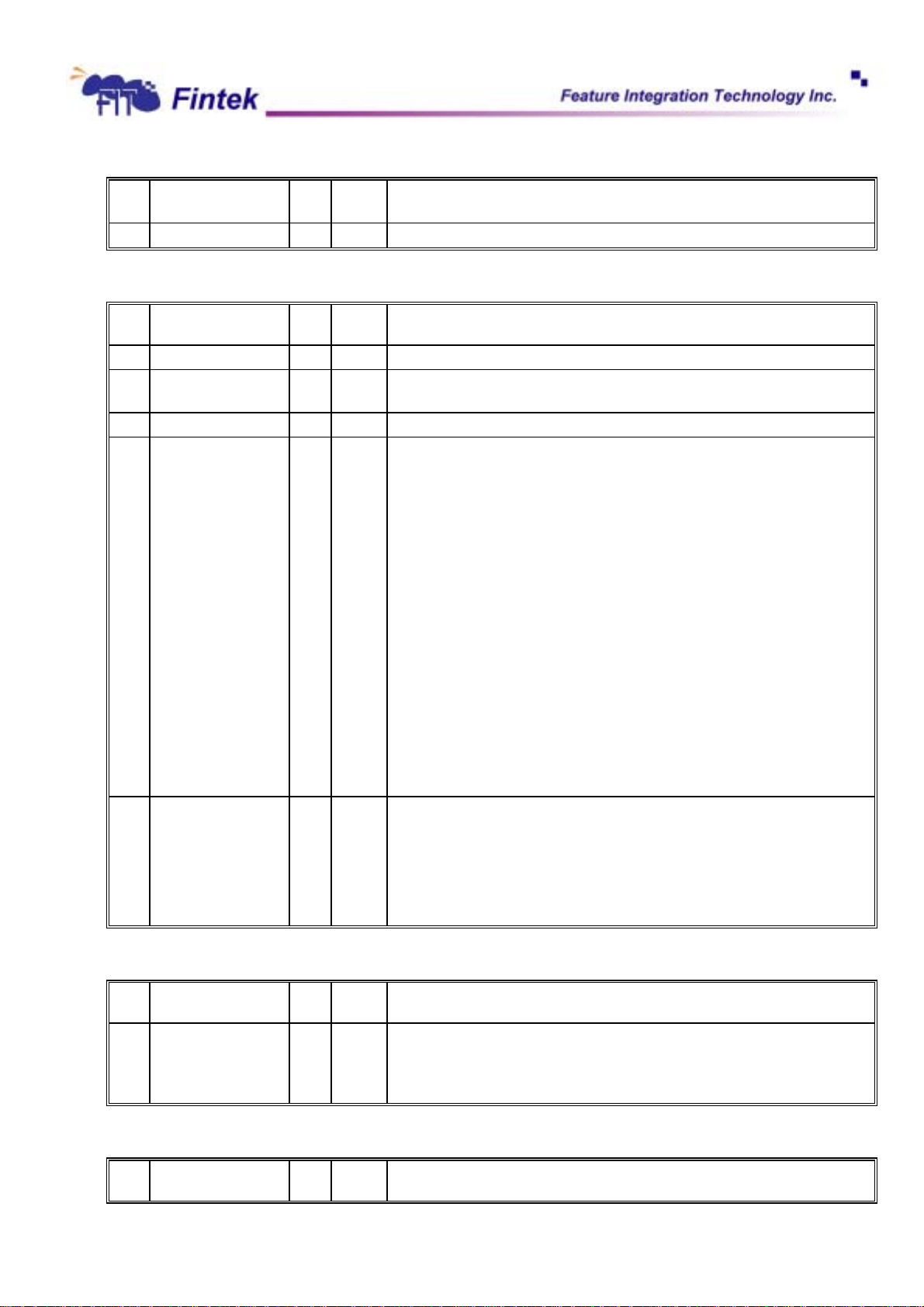
1 DRV1_BUSY R 0 FDD number 1 is in seek or calibration condition. FDD number 1 is not support
0 DRV0_BUSY R 0 FDD number 0 is in seek or calibration condition.
7.2.3.8 Data Rate Select Register Base + 4
Bit Name R/W Default Description
7 SOFTRST W 0 A 1 written to this bit will software reset the controller. Auto clear after reset.
6 PWRDOWN W 0 A 1 to this bit will put the controller into low power mode which will turn off the
5 Reserved - - Return 0 when read.
4-2 PRECOMP W 000 Select the value of write precompensation:
1-0 DRATE W 10 Data rate select:
F71805
in this design.
oscillator and data separator circuits.
250K-1Mbps 2Mbps
000: default delays default delays
001: 41.67ns 20.8ns
010: 83.34ns 41.17ns
011: 125.00ns 62.5ns
100: 166.67ns 83.3ns
101: 208.33ns 104.2ns
110: 250.00ns 125.00ns
111: 0.00ns (disabled) 0.00ns (disabled)
The default value of corresponding data rate:
250Kbps: 125ns
300Kbps: 125ns
500Kbps: 125ns
1Mbps: 41.67ns
2Mbps: 20.8ns
MFM FM
00: 500Kbps 250Kbps
01: 300Kbps 150Kbps
10: 250Kbps 125Kbps
11: 1Mbps illegal
7.2.3.9 Data (FIFO) Register Base + 5
Bit Name R/W Default Description
7-0 DATA R/W 00h The FIFO is used to transfer all commands, data and status between controller
and the system. The Data Register consists of four status registers in a stack
with only one register presented to the data bus at a time. The FIFO is default
disabled and could be enabled via the CONFIGURE command.
Status Registers 0
Bit Name R/W Default Description
28
Dec., 2006
V0.25P
Page 31
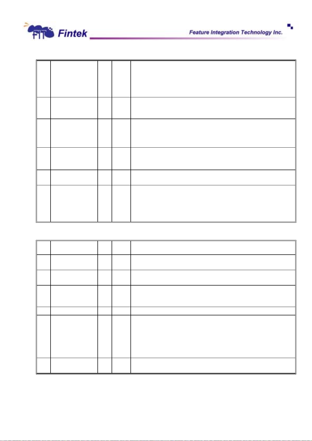
7-6 IC R - Interrupt code :
5 SE R - Seek end.
4 EC R - Equipment check.
3 NR R - Not ready.
2 HD R - Head address.
1-0 DS R - Drive select.
F71805
00: Normal termination of command.
01: Abnormal termination of command.
10: Invalid command.
11: Abnormal termination caused by poling.
Set when a SEEK or RECALIBRATE or a READ or WRITE with implied seek
command is completed.
0: No error
1: When a fault signal is received form the FDD or the TRK0# signal fails to
occur after 77 step pulses.
0: Drive is ready
1: Drive is not ready.
The current head address.
00: Drive A selected.
01: Drive B selected.
10: Drive C selected.
11: Drive D selected.
Status Registers 1
Bit Name R/W Default Description
7 EN R - End of Track.
Set when the FDC tries to access a sector beyond the final sector of a cylinder.
6 DE R - Data Error.
The FDC detect a CRC error in either the ID field or the data field of a sector.
4 OR R - Overrun/Underrun.
Set when the FDC is not serviced by the host system within a certain time
interval during data transfer.
3 Reserved - - Unused. This bit is always “0”
2 ND R - No Data.
Set when the following conditions occurred:
1. The specified sector is not found during any read command.
2. The ID field cannot be read without errors during a READ ID command.
3. The proper sector sequence cannot be found during a READ TRACK
command.
1 NW R - No Writable
Set when WPT# is active during execution of write commands.
29
Dec., 2006
V0.25P
Page 32
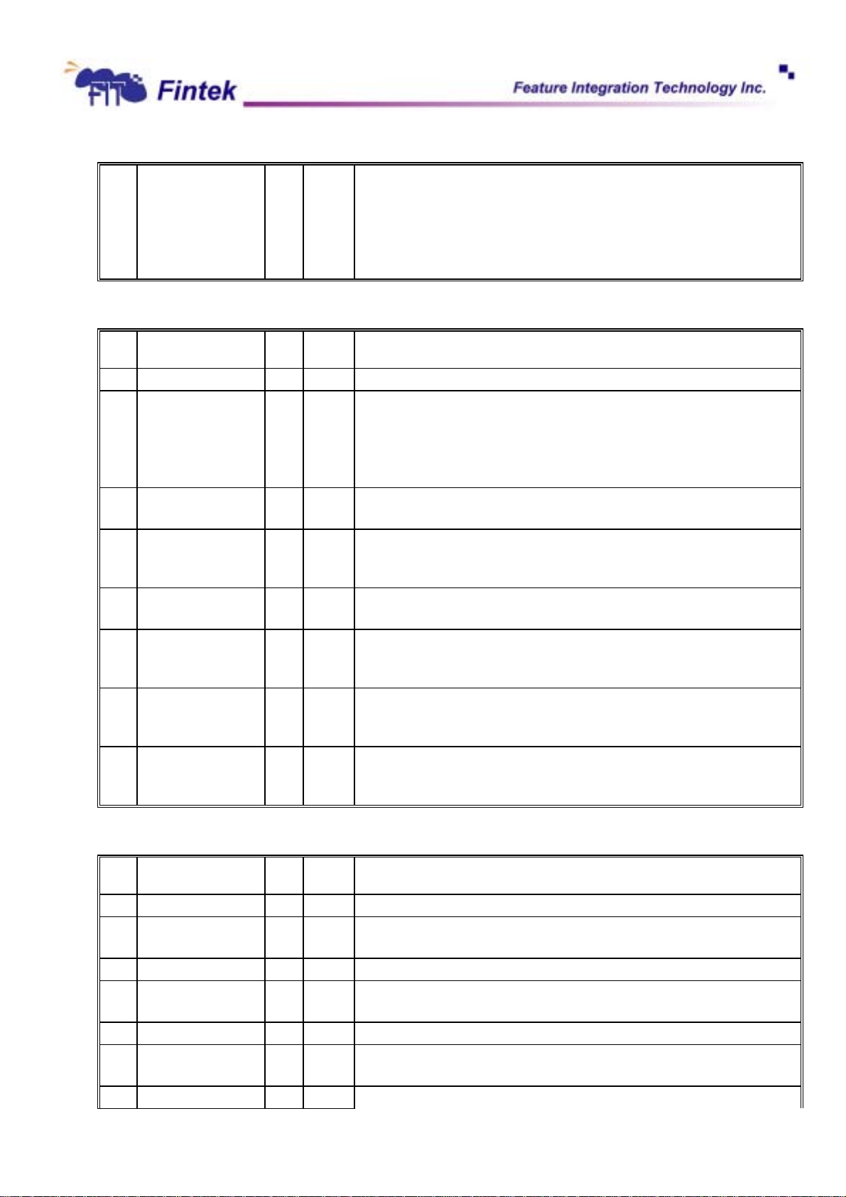
0 MA R - Missing Address Mark.
Status Registers 2
Bit Name R/W Default Description
7 Reserved - - Unused. This bit is always “0”.
6 CM R - Control Mark.
5 DD R - Data Error in Data Field.
4 WC R - Wrong Cylinder.
3 SE R - Scan Equal.
2 SN R - Scan Not Satisfied.
1 BC R - Bad Cylinder.
0 MD R - Missing Data Address Mark.
F71805
Set when the following conditions occurred:
1. Cannot detect an ID address mark at the specified track after
encountering the index pulse form the INDEX# pin twice.
2. Cannot detect a data address mark or a deleted data address mark on the
specified track.
Set when following conditions occurred:
1. Encounters a deleted data address mark during a READ DATA command.
2. Encounters a data address mark during a READ DELETED DATA
command.
The FDC detects a CRC error in the data field.
Set when the track address from the sector ID field is different from the track
address maintained inside the FDC.
Set if the equal condition is satisfied during execution of the SCAN command.
Set when the FDC cannot find a sector on the track which meets the desired
condition during any scan command.
The track address from the sector ID field is different from the track address
maintained inside the FDC and is equal to FFh which indicates a bad track.
Set when the FDC cannot detect a data address mark or a deleted data
address mark.
Status Registers 3
Bit Name R/W Default Description
7 Reserved - - Unused. This bit is always “0”.
6 WP R - Write Protect.
Indicates the status of WPT# pin.
5 Reserved R - Unused. This bit is always “1”.
4 T0 R - Track 0.
Indicates the status of the TRK0# pin.
3 Reserved. R - Unused. This bit is always “1”.
2 HD R - Head Address.
Indicates the status of the HDSEL# pin.
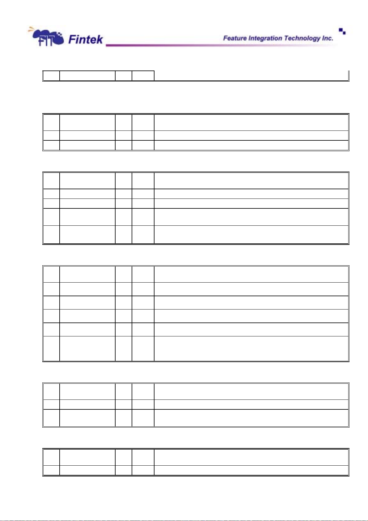
1 DS1 R - Drive Select.
30
Dec., 2006
V0.25P
Page 33
F71805
0 DS0 R -
These two bits indicate the DS1, DS0 bits in the command phase.
7.2.3.10 Digital Input Register (PC-AT Mode) Base + 7
Bit Name R/W Default Description
7 DSKCHG R - This bit indicates the complement of DSKCHG# disk interface input.
6-0 Reserved - - Reserved.
7.2.3.11 Digital Input Register (PS/2 Mode) Base + 7
Bit Name R/W Default Description
7 DSKCHG R - This bit indicates the complement of DSKCHG# disk interface input.
6-3 Reserved - - Reserved.
2-1 DRATE R 10 These bits indicate the status of the DRATE programmed through the Data
Rate Select Register or Configuration Control Register.
0 HIGHDEN_N R 1 0: 1Mbps or 500Kbps data rate is chosen.
1: 300Kbps or 250Kbps data rate is chosen.
7.2.3.12 Digital Input Register (Model 30 Mode) Base + 7
Bit Name R/W Default Description
7 DSKCHG_N R - This bit indicates the state of DSKCHG# disk interface input.
6-4 Reserved - - Reserved.
3 DMAEN R 0 This bit reflects the DMA bit in Digital Output Register.
2 NOPRE R 0 This bit reflects the NOPRE bit in Configuration Control Register.
1-0 DRATE R 10 These bits indicate the status of DRATE programmed through the Data Rate
Select Register or Configuration Control Register.
7.2.3.13 Configuration Control Register (PC-AT and PS/2 Mode) Base + 7
Bit Name R/W Default Description
7-2 Reserved - - Reserved.
1-0 DRATE W 10 These bit determine the data rate of the floppy controller. See DRATE bits in
Data Rate Select Register.
7.2.3.14 Configuration Control Register (Model 30 Mode) Base + 7
Bit Name R/W Default Description
7-3 Reserved - - Reserved.
31
Dec., 2006
V0.25P
Page 34

2 NOPRE W 0 This bit could be programmed through Configuration Control Register and be
1-0 DRATE W 10 These bit determine the data rate of the floppy controller. See DRATE bits in
7.2.3.15 FDC Commands
Terminology:
C Cylinder Number 0 -256
D Data Pattern
DIR Step Direction
0: step out
1: step in
DS0 Drive Select 0
DS1 Drive Select 1
DTL Data Length
EC Enable Count
EOT End of Track
EFIFO Enable FIFO
0: FIFO is enabled.
1: FIFO is disabled.
EIS Enable Implied Seek
FIFOTHR FIFO Threshold
GAP Alters Gap Length
GPL Gap Length
H/HDS Head Address
HLT Head Load Time
HUT Head Unload Time
LOCK Lock EFIFO, FIFOTHR, PTRTRK bits.
Prevent these bits from being affected by software reset.
MFM MFM or FM mode
0: FM
1: MFM
MT Multi-Track
N Sector Size Code. All values up to 07h are allowable.
00: 128 bytes
01: 256 bytes
.. ..
07 16 Kbytes
NCN New Cylinder Number
ND Non-DMA Mode
OW Overwritten
PCN Present Cylinder Number
POLL Polling disable
0: polling is enabled.
1: polling is disabled.
PRETRK Precompensation Start Track Number
R Sector address
RCN Relative Cylinder Number
SC Sector per Cylinder
SK Skip deleted data address mark
SRT Step Rate Time
F71805
read through the bit 2 in Digital Input Register in Model 30 Mode. But it has no
functionality.
Data Rate Select Register.
32
Dec., 2006
V0.25P
Page 35

ST0 Status Register 0
ST1 Status Register 1
ST2 Status Register 2
ST3 Status Register 3
WGATE Write Gate alters timing of WE.
Read Data
Phase R/W D7 D6 D5 D4 D3 D2 D1 D0 Remark
Command W MT MFM SK 0 0 1 1 0 Command code
W 0 0 0 0 0 HDS DS1 DS0
F71805
W ----------------------------- C ---------------------------
W ----------------------------- H ---------------------------
W ----------------------------- R ---------------------------
W ------------------------------ N ---------------------------
W ---------------------------- EOT --------------------------
W ---------------------------- GPL --------------------------
W ---------------------------- DTL --------------------------
Execution Data transfer between
Result R ---------------------------- ST0 --------------------------
R ----------------------------- ST1 --------------------------
R ---------------------------- ST2 --------------------------
R ----------------------------- C ---------------------------
R ----------------------------- H ---------------------------
R ----------------------------- R ---------------------------
R ----------------------------- N ---------------------------
Sector ID information
prior to command
execution
the FDD and system
Status information
after command
execution.
Sector ID information
after command
execution.
Read Deleted Data
Phase R/W D7 D6 D5 D4 D3 D2 D1 D0 Remark
Command W MT MFM SK 0 1 1 0 0 Command code
W 0 0 0 0 0 HDS DS1 DS0
W ----------------------------- C ---------------------------
W ----------------------------- H ---------------------------
W ----------------------------- R ---------------------------
W ------------------------------ N ---------------------------
33
Sector ID information
prior to command
execution
Dec., 2006
V0.25P
Page 36

F71805
Execution Data transfer between
Result R ---------------------------- ST0 --------------------------
Read A Track
Phase R/W D7 D6 D5 D4 D3 D2 D1 D0 Remark
Command W 0 MFM 0 0 0 0 1 0 Command code
W ---------------------------- EOT --------------------------
W ---------------------------- GPL --------------------------
W ---------------------------- DTL --------------------------
R ----------------------------- ST1 --------------------------
R ---------------------------- ST2 --------------------------
R ----------------------------- C ---------------------------
R ----------------------------- H ---------------------------
R ----------------------------- R ---------------------------
R ----------------------------- N ---------------------------
the FDD and system
Status information
after command
execution.
Sector ID information
after command
execution.
W 0 0 0 0 0 HDS DS1 DS0
W ----------------------------- C ---------------------------
W ----------------------------- H ---------------------------
Sector ID information
prior to command
execution
W ----------------------------- R ---------------------------
W ------------------------------ N ---------------------------
W ---------------------------- EOT --------------------------
W ---------------------------- GPL --------------------------
W ---------------------------- DTL --------------------------
Execution Data transfer between
the FDD and system.
FDD reads contents
of all cylinders from
index hole to EOT.
Result R ---------------------------- ST0 --------------------------
R ----------------------------- ST1 --------------------------
Status information
after command
execution.
R ---------------------------- ST2 --------------------------
R ----------------------------- C ---------------------------
R ----------------------------- H ---------------------------
Sector ID information
after command
execution.
R ----------------------------- R ---------------------------
R ----------------------------- N ---------------------------
34
Dec., 2006
V0.25P
Page 37

Read ID
Phase R/W D7 D6 D5 D4 D3 D2 D1 D0 Remark
Command W 0 MFM 0 0 1 0 1 0 Command code
W 0 0 0 0 0 HDS DS1 DS0
Execution The first correct ID
Result R ---------------------------- ST0 --------------------------
R ----------------------------- ST1 --------------------------
R ---------------------------- ST2 --------------------------
F71805
information on the
cylinder is stored in
Data Register.
Status information
after command
execution.
R ----------------------------- C ---------------------------
R ----------------------------- H ---------------------------
Disk status after the
command has been
completed.
R ----------------------------- R ---------------------------
R ----------------------------- N ---------------------------
Verify
Phase R/W D7 D6 D5 D4 D3 D2 D1 D0 Remark
Command W MT MFM SK 1 0 1 1 0 Command code
W EC 0 0 0 0 HDS DS1 DS0
W ----------------------------- C ---------------------------
W ----------------------------- H ---------------------------
W ----------------------------- R ---------------------------
W ------------------------------ N ---------------------------
W ---------------------------- EOT --------------------------
Sector ID information
prior to command
execution
W ---------------------------- GPL --------------------------
W -------------------------- DTL/SC ------------------------
Execution No data transfer
Result R ---------------------------- ST0 --------------------------
R ----------------------------- ST1 --------------------------
Status information
after command
execution.
R ---------------------------- ST2 --------------------------
R ----------------------------- C ---------------------------
R ----------------------------- H ---------------------------
35
Sector ID information
after command
execution.
Dec., 2006
V0.25P
Page 38
F71805
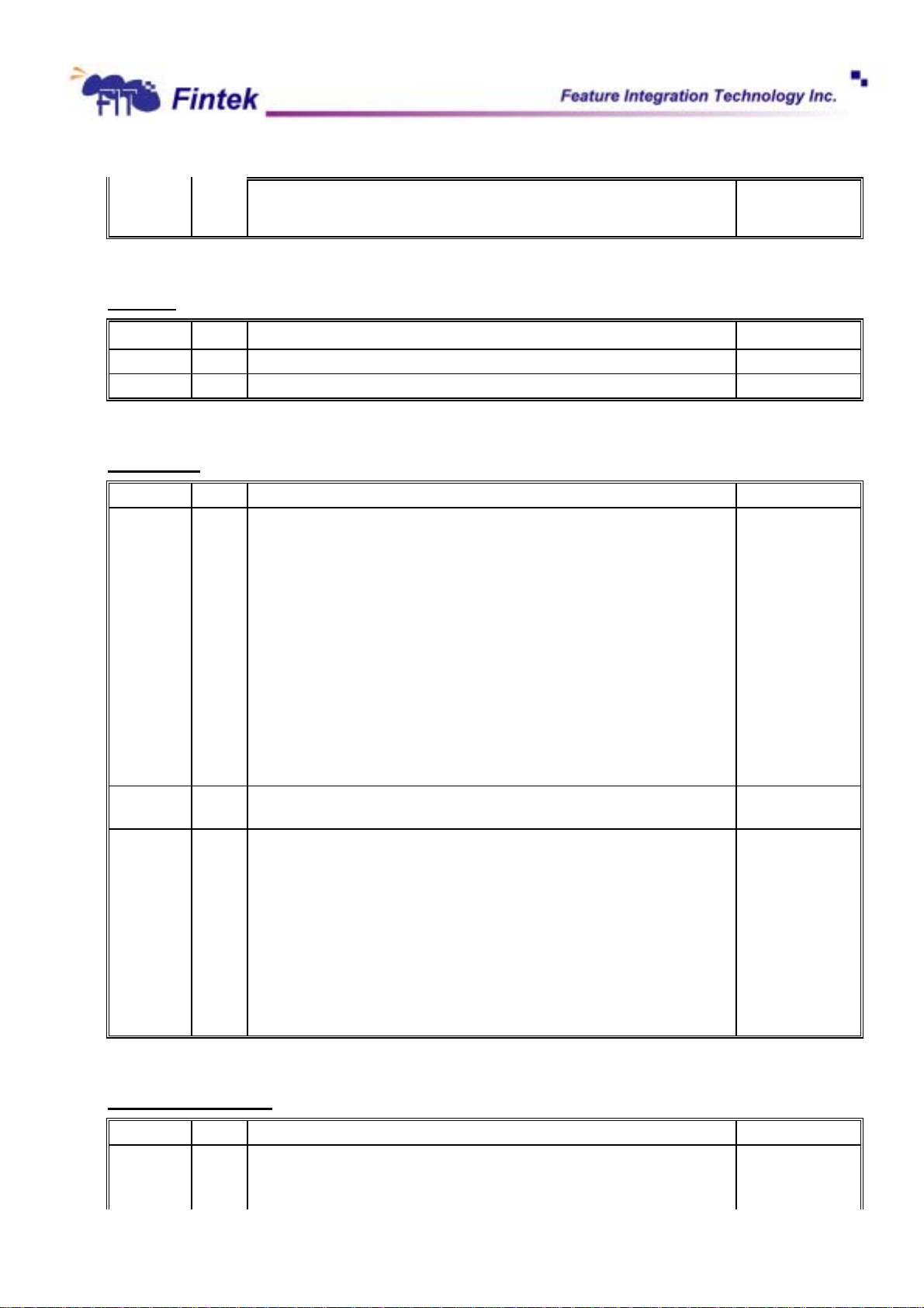
Version
Write Data
R ----------------------------- R ---------------------------
R ----------------------------- N ---------------------------
Phase R/W D7 D6 D5 D4 D3 D2 D1 D0 Remark
Command W 0 0 0 1 0 0 0 0 Command code
Result R 1 0 0 1 0 0 0 0 Enhanced controller
Phase R/W D7 D6 D5 D4 D3 D2 D1 D0 Remark
Command W MT MFM 0 0 0 1 0 1 Command code
W 0 0 0 0 0 HDS DS1 DS0
W ----------------------------- C ---------------------------
W ----------------------------- H ---------------------------
W ----------------------------- R ---------------------------
Sector ID information
prior to command
execution
W ------------------------------ N ---------------------------
W ---------------------------- EOT --------------------------
W ---------------------------- GPL --------------------------
W ---------------------------- DTL --------------------------
Execution Data transfer between
Result R ---------------------------- ST0 --------------------------
R ----------------------------- ST1 --------------------------
R ---------------------------- ST2 --------------------------
R ----------------------------- C ---------------------------
R ----------------------------- H ---------------------------
R ----------------------------- R ---------------------------
R ----------------------------- N ---------------------------
Write Deleted Data
the FDD and system.
Status information
after command
execution.
Sector ID information
after command
execution.
Phase R/W D7 D6 D5 D4 D3 D2 D1 D0 Remark
Command W MT MFM 0 0 1 0 0 1 Command code
W 0 0 0 0 0 HDS DS1 DS0
36
Dec., 2006
V0.25P
Page 39

F71805
W ----------------------------- C ---------------------------
W ----------------------------- H ---------------------------
Sector ID information
prior to command
execution
W ----------------------------- R ---------------------------
W ------------------------------ N ---------------------------
W ---------------------------- EOT --------------------------
W ---------------------------- GPL --------------------------
W ---------------------------- DTL --------------------------
Execution Data transfer between
the FDD and system.
Result R ---------------------------- ST0 --------------------------
R ----------------------------- ST1 --------------------------
Status information
after command
execution.
R ---------------------------- ST2 --------------------------
R ----------------------------- C ---------------------------
R ----------------------------- H ---------------------------
Sector ID information
after command
execution.
R ----------------------------- R ---------------------------
R ----------------------------- N ---------------------------
Format A Track
Phase R/W D7 D6 D5 D4 D3 D2 D1 D0 Remark
Command W 0 MFM 0 0 1 1 0 1 Command code
W 0 0 0 0 0 HDS DS1 DS0
W ------------------------------ N --------------------------- Bytes/Sector
W ---------------------------- SC -------------------------- Sectors/Cylinder
W ---------------------------- GPL -------------------------- Gap 3 Length
W ----------------------------- D --------------------------- Data Pattern
Execution
for each
sector
( repeat )
Result R ---------------------------- ST0 --------------------------
R ----------------------------- ST1 --------------------------
R ---------------------------- ST2 --------------------------
------------------------------ C ---------------------------
W ------------------------------ H ---------------------------
W ------------------------------ R ---------------------------
W ----------------------------- N --------------------------
Input sector
parameter.
Status information
after command
execution.
R ------------------------- Undefined ----------------------
R ------------------------- Undefined ----------------------
37
Dec., 2006
V0.25P
Page 40
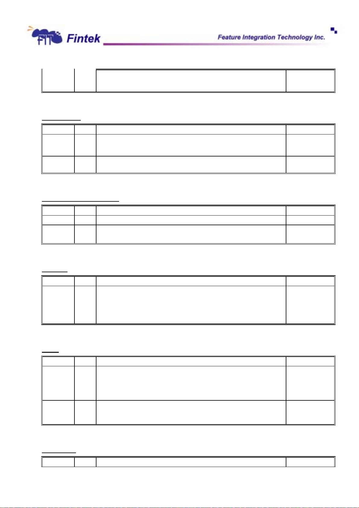
F71805
R -------------------------- Undefined -----------------------
R ------------------------- Undefined ----------------------
Recalibrate
Phase R/W D7 D6 D5 D4 D3 D2 D1 D0 Remark
Command W 0 0 0 0 0 1 1 1 Command code
W 0 0 0 0 0 0 DS1 DS0
Execution Head retracted to
Sense Interrupt Status
Phase R/W D7 D6 D5 D4 D3 D2 D1 D0 Remark
Command W 0 0 0 0 1 0 0 0 Command code
Result R ---------------------------- ST0 --------------------------
R ---------------------------- PCN --------------------------
track 0
Specify
Phase R/W D7 D6 D5 D4 D3 D2 D1 D0 Remark
Command W 0 0 0 0 0 0 1 1 Command code
W |------------------ SRT -------------------| |------------------ HUT -------------------|
W |------------------------------------- SRT ---------------------------------------| ND
Seek
Phase R/W D7 D6 D5 D4 D3 D2 D1 D0 Remark
Command W 0 0 0 0 1 1 1 1 Command code
W 0 0 0 0 0 HDS DS1 DS0
W ---------------------------- NCN --------------------------
Execution Head positioned over
proper cylinder on
diskette
Configure
Phase R/W D7 D6 D5 D4 D3 D2 D1 D0 Remark
38
Dec., 2006
V0.25P
Page 41
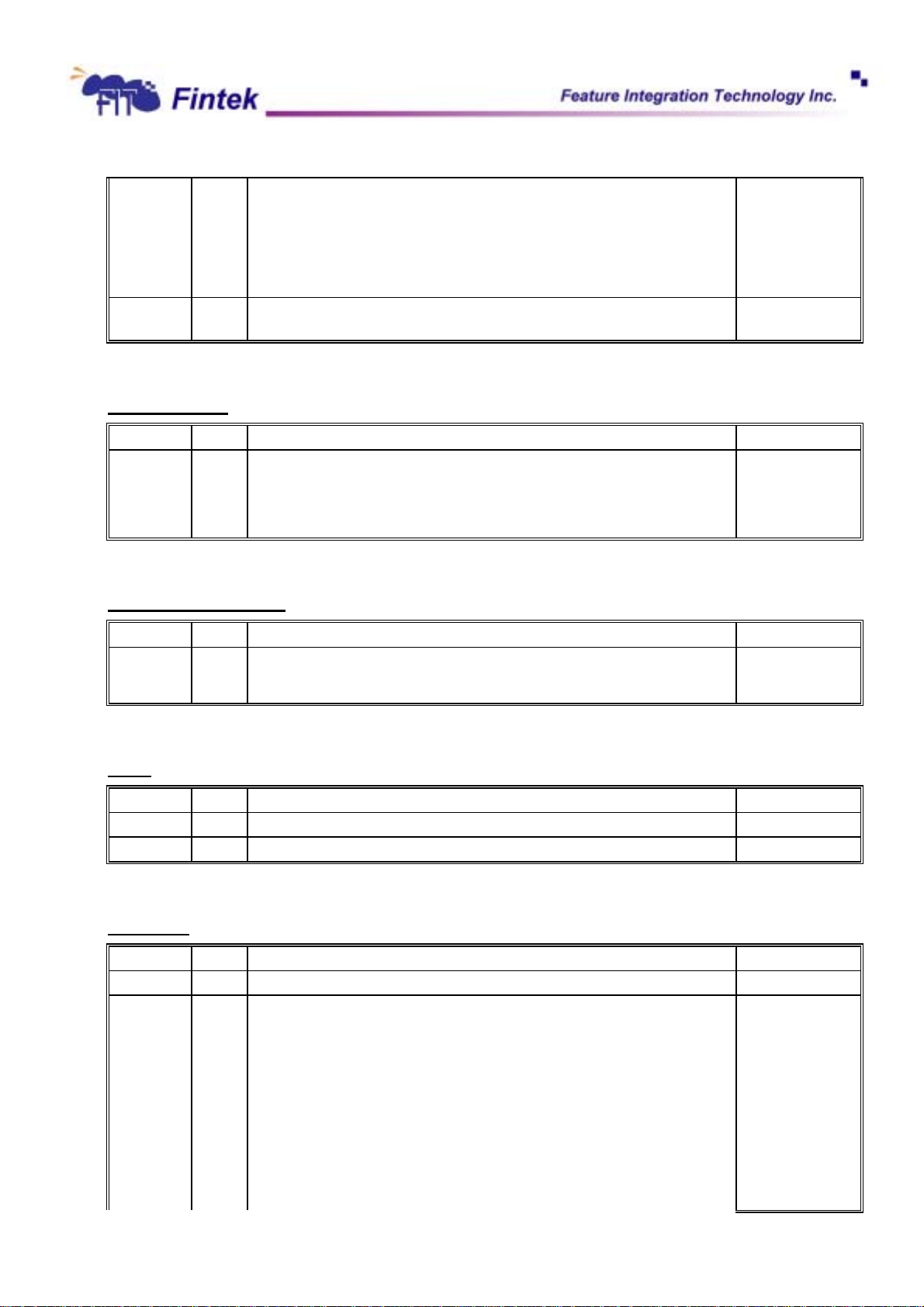
Command W 0 0 0 1 0 0 1 1 Command code
W 0 0 0 0 0 HDS DS1 DS0
W 0 EIS EFIFO POLL |---------------- FIFOTHR ---------------|
W ---------------------------- PRETRK --------------------------
Execution Internal registers
Relative Seek
Phase R/W D7 D6 D5 D4 D3 D2 D1 D0 Remark
Command W 1 DIR 0 0 1 1 1 1 Command code
F71805
written
W 0 0 0 0 0 HDS DS1 DS0
W ---------------------------- RCN --------------------------
Perpendicular Mode
Phase R/W D7 D6 D5 D4 D3 D2 D1 D0 Remark
Command W 0 0 0 1 0 0 1 0 Command code
W OW 0 D3 D2 D1 D0 GAP WGATE
Lock
Phase R/W D7 D6 D5 D4 D3 D2 D1 D0 Remark
Command W LOCK 0 0 1 0 1 0 0 Command code
Result R 0 0 0 LOCK 0 0 0 0
Dumpreg
Phase R/W D7 D6 D5 D4 D3 D2 D1 D0 Remark
Command W 0 0 0 0 1 1 1 0 Command code
Result R -------------------------- PCN ( Drive 0 ) ------------------------
R -------------------------- PCN ( Drive 0 ) ------------------------
R -------------------------- PCN ( Drive 0 ) ------------------------
R -------------------------- PCN ( Drive 0 ) ------------------------
R |------------------ SRT -------------------| |------------------ HUT -------------------|
R |------------------------------------- SRT ---------------------------------------| ND
R -------------------------- SC/EOT ------------------------
39
Dec., 2006
V0.25P
Page 42
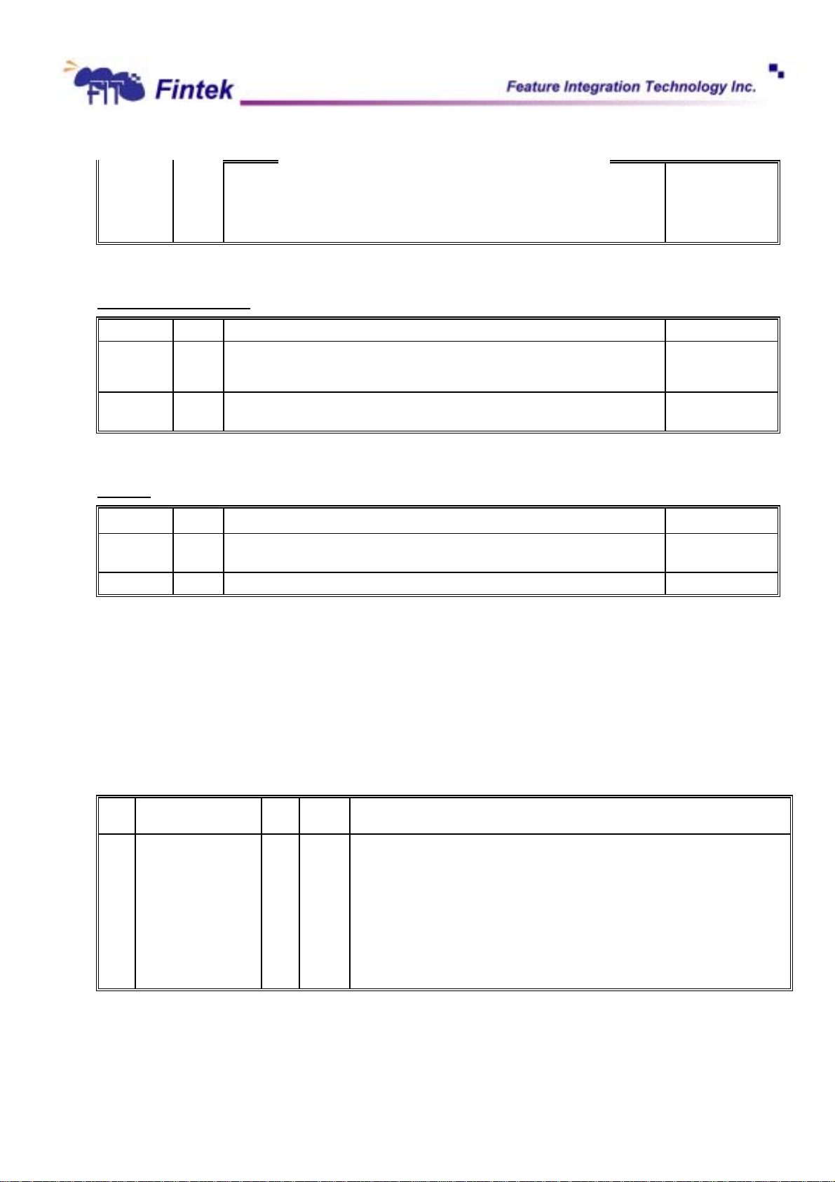
F71805
R LOCK 0 D3 D2 D1 D0 GAP WGATE
R 0 EIS EFIFO POLL |---------------- FIFOTHR ---------------|
R ---------------------------- PRETRK --------------------------
Sense Drive Status
Phase R/W D7 D6 D5 D4 D3 D2 D1 D0 Remark
Command W 0 0 0 0 0 1 0 0 Command code
W 0 0 0 0 0 HDS DS1 DS0
Result R ---------------------------- ST3 -------------------------- Status information
Invalid
Phase R/W D7 D6 D5 D4 D3 D2 D1 D0 Remark
Command W ---------------------------- Invalid Codes -------------------------- FDC goes to standby
Result R ---------------------------- ST0 -------------------------- ST0 = 80h
abut disk drive
state.
7.3 UART 1 Register
7.3.1 Logic Device Number Register
Logic Device Number Register Index 07h
Bit Name R/W Default Description
7-0 LDN R/W 00h 00h: Select FDC device configuration registers.
01h: Select UART 1 device configuration registers.
02h: Select UART 2 device configuration registers.
03h: Select Parallel Port device configuration registers.
04h: Select Hardware Monitor device configuration registers.
06h: Select GPIO device configuration registers.
0ah: Select PME device configuration registers.
Otherwise: reserved.
40
Dec., 2006
V0.25P
Page 43
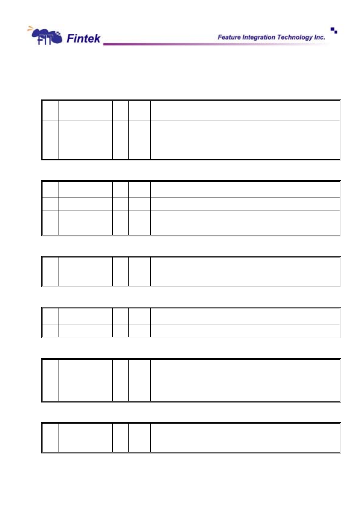
7.3.2 UART 1 Configuration Register
UART IRQ Sharing Register Index 26h
Bit Name R/W Default Description
7-2 Reserved - -
1 IRQ_MODE R/W 0
0 IRQ_SHAR R/W 0
Reserved.
0: PCI IRQ sharing mode (low level).
1: ISA IRQ sharing mode (low pulse).
0: disable IRQ sharing of two UART devices.
1: enable IRQ sharing of two UART devices.
UART 1 Device Enable Register Index 30h
Bit Name R/W Default Description
F71805
7-1 Reserved - - Reserved
0 UR1_EN R/W 1 0: disable UART 1.
1: enable UART 1.
Base Address High Register Index 60h
Bit Name R/W Default Description
7-0 BASE_ADDR_HI R/W 03h The MSB of UART 1 base address.
Base Address Low Register Index 61h
Bit Name R/W Default Description
7-0 BASE_ADDR_LO R/W F8h The LSB of UART 1 base address.
IRQ Channel Select Register Index 70h
Bit Name R/W Default Description
7-4 Reserved - - Reserved.
3-0 SELUR1IRQ R/W 4h Select the IRQ channel for UART 1.
RS485 Enable Register Index F0h
Bit Name R/W Default Description
7-5 Reserved - - Reserved.
41
Dec., 2006
V0.25P
Page 44
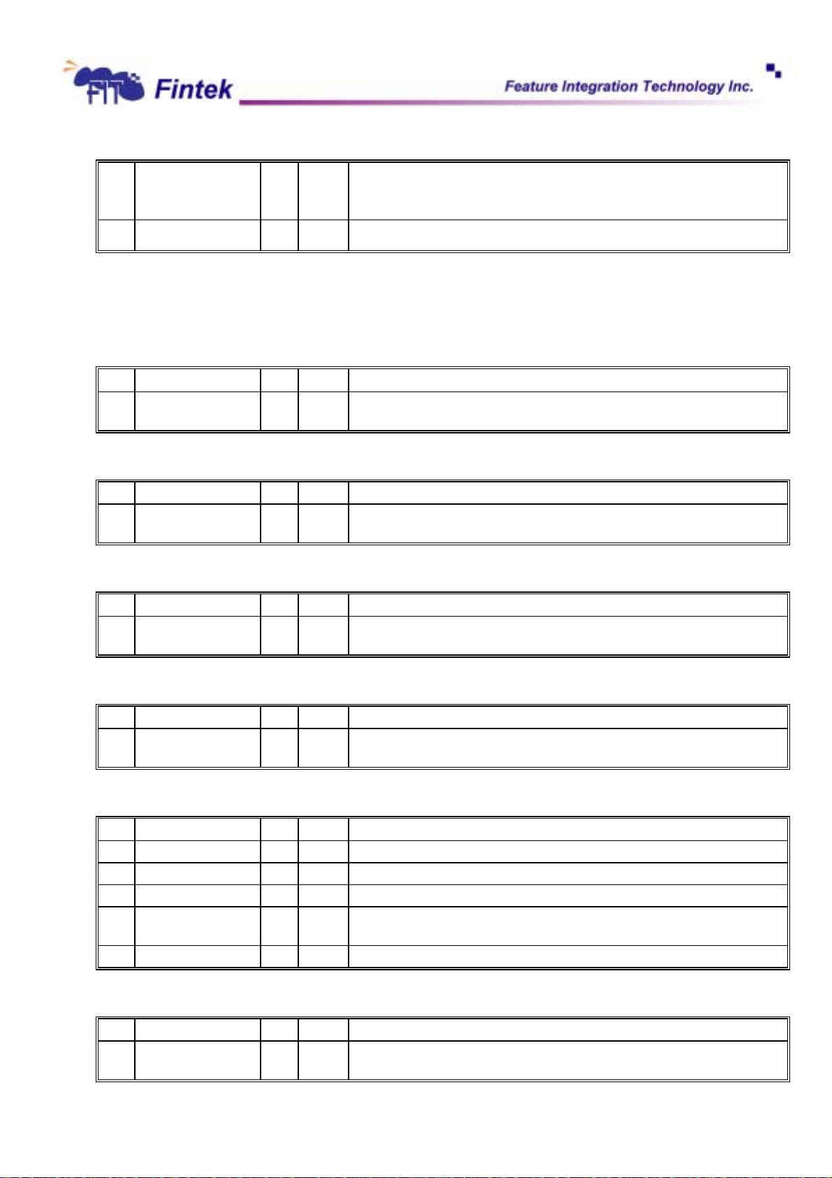
4 RS485_EN R/W 0 0: RS232 driver.
3-0 Reserved - - Reserved.
7.3.3 Device Registers
F71805
1: RS485 driver. Auto drive RTS# low when transmitting data.
7.3.3.1 Receiver Buffer Register
Bit Name R/W Default Description
7-0 RBR R 00h
Base + 0
The data received.
Read only when LCR[7] is 0
7.3.3.2 Transmitter Holding Register Base + 0
Bit Name R/W Default Description
7-0 THR W 00h
Data to be transmitted.
Write only when LCR[7] is 0
7.3.3.3 Divisor Latch (LSB) Base + 0
Bit Name R/W Default Description
7-0 DLL R/W 01h
Baud generator divisor low byte.
Access only when LCR[7] is 1.
7.3.3.4 Divisor Latch (MSB) Base + 1
Bit Name R/W Default Description
7-0 DLM R/W 00h
Baud generator divisor high byte.
Access only when LCR[7] is 1.
7.3.3.5 Interrupt Enable Register Base + 1
Bit Name R/W Default Description
7-4 Reserved - - Reserved.
3 EDSSI R/W 0 Enable Modem Status Interrupt. Access only when LCR[7] is 0.
2 ELSI R/W 0 Enable Line Status Error Interrupt. Access only when LCR[7] is 0.
1 ETBFI R/W 0 Enable Transmitter Holding Register Empty Interrupt. Access only when
LCR[7] is 0.
0 ERBFI R/W 0 Enable Received Data Available Interrupt. Access only when LCR[7] is 0.
7.3.3.6 Interrupt Identification Register Base + 2
Bit Name R/W Default Description
7 FIFO_EN R 0
0: FIFO is disabled
1: FIFO is enabled.
42
Dec., 2006
V0.25P
Page 45
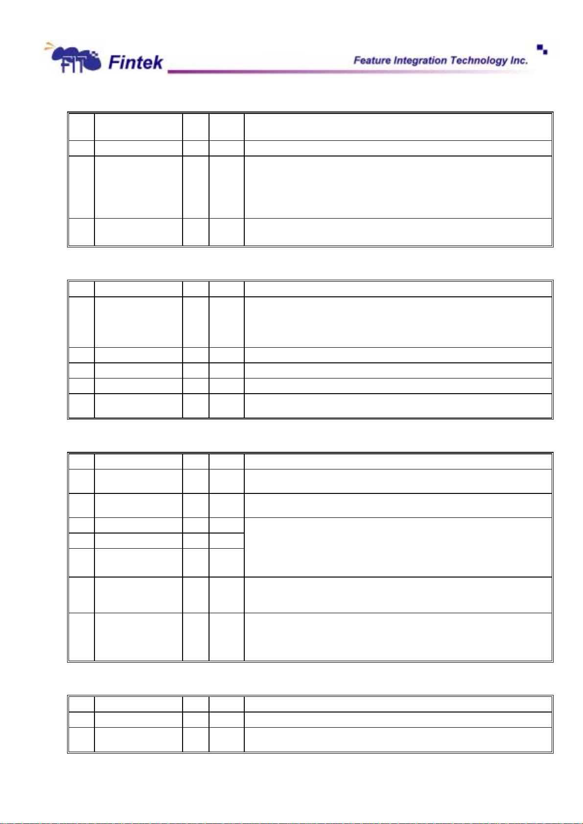
F71805
6 FIFO_EN R 0
5-4 Reserved - - Reserved.
3-1 IRQ_ID R 000
0 IRQ_PENDN R 1
0: FIFO is disabled
1: FIFO is enabled.
000: Interrupt is caused by Modem Status
001: Interrupt is caused by Transmitter Holding Register Empty
010: Interrupt is caused by Received Data Available.
110: Interrupt is caused by Character Timeout
011: Interrupt is caused by Line Status.
1: Interrupt is not pending.
0: Interrupt is pending.
7.3.3.7 FIFO Control Register Base + 2
Bit Name R/W Default Description
7-6 RCV_TRIG W 00
5-3 Reserved - - Reserved.
2 CLRTX R 0
1 CLRRX R 0
0 FIFO_EN R 0
00: Receiver FIFO trigger level is 1.
01: Receiver FIFO trigger level is 4.
10: Receiver FIFO trigger level is 8.
11: Receiver FIFO trigger level is 14.
Reset the transmitter FIFO.
Reset the receiver FIFO.
0: Disable FIFO.
1: Enable FIFO.
7.3.3.8 Line Control Register Base + 3
Bit Name R/W Default Description
7 DLAB R/W 0
6 SETBRK R/W 0
5 STKPAR R/W 0
4 EPS R/W 0
3 PEN R/W 0
2 STB R/W 0
1-0 WLS R/W 00
0: Divisor Latch can’t be accessed.
1: Divisor Latch can be accessed via Base and Base+1.
0: Transmitter is in normal condition.
1: Transmit a break condition.
XX0: Parity Bit is disable
001: Parity Bit is odd.
011: Parity Bit is even
101: Parity Bit is logic 1
111: Parity Bit is logic 0
0: Stop bit is one bit
1: When word length is 5 bit stop bit is 1.5 bit
else stop bit is 2 bit
00: Word length is 5 bit
01: Word length is 6 bit
10: Word length is 7 bit
11: Word length is 8 bit
7.3.3.9 MODEM Control Register Base + 4
Bit Name R/W Default Description
7-5 Reserved R/W -
4 LOOP R/W 0
Reserved.
0: UART in normal condition.
1: UART is internal loop back
43
Dec., 2006
V0.25P
Page 46
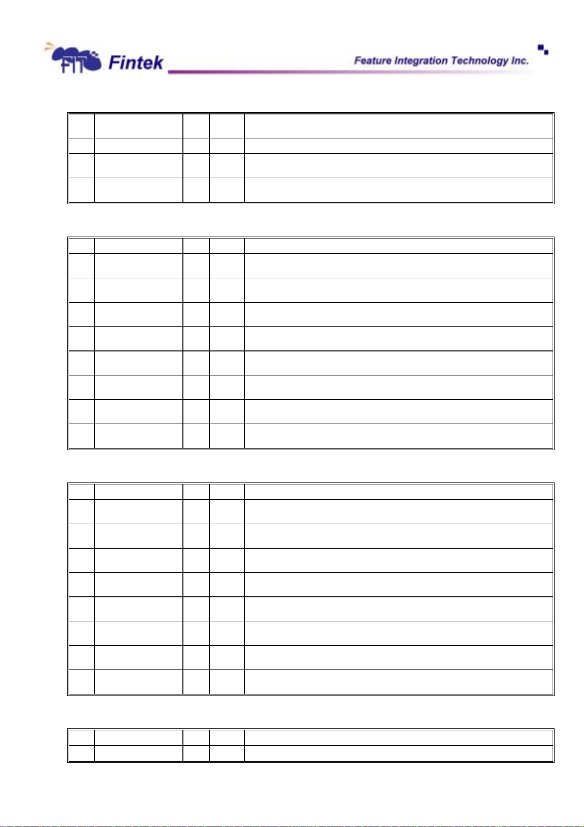
F71805
3 OUT2 R/W 0
2 OUT1 R/W 0
1 RTS R/W 0
0 DTR R/W 0
0: All interrupt is disabled.
1: Interrupt is enabled(disabled) by IER.
Read from MSR[6] is loop back mode
0: RTS# is forced to logic 1
1: RTS# is forced to logic 0
0: DTR# is forced to logic 1
1: DTR# is forced to logic 0
7.3.3.10 Line Status Register Base + 5
Bit Name R/W Default Description
7 RCR_ERR R 0
6 TEMT R 1
5 THRE R 1
4 BI R 0
3 FE R 0
2 PE R 0
1 OE R 0
0 DR R 0
0: No error in the FIFO when FIFO is enabled
1: Error in the FIFO when FIFO is enabled.
0: Transmitter is in transmitting.
1: Transmitter is empty.
0: Transmitter Holding Register is not empty.
1: Transmitter Holding Register is empty.
0: No break condition detected.
1: A break condition is detected.
0: Data received has no frame error.
1: Data received has frame error.
0: Data received has no parity error.
1: Data received has parity error.
0: No overrun condition occurred.
1: An overrun condition occurred.
0: No data is ready for read.
1: Data is received.
7.3.3.11 MODEM Status Register Base + 6
Bit Name R/W Default Description
7 DCD R -
6 RI R -
5 DSR R -
4 CTS R -
3 DDCD R 0
2 TERI R 0
1 DDSR R 0
0 DCTS R 0
Complement of DCD# input. In loop back mode, this bit is equivalent to OUT2
in MCR.
Complement of RI# input. In loop back mode , this bit is equivalent to OUT1 in
MCR
Complement of DSR# input. In loop back mode , this bit is equivalent to DTR in
MCR
Complement of CTS# input. In loop back mode , this bit is equivalent to RTS in
MCR
0: No state changed at DCD#.
1: State changed at DCD#.
0: No Trailing edge at RI#.
1: A low to high transition at RI#.
0: No state changed at DSR#.
1: State changed at DSR#.
0: No state changed at CTS#.
1: State changed at CTS#.
7.3.3.12 Scratch Register Base + 7
Bit Name R/W Default Description
7-0 SCR R/W 00h
Scratch register.
44
Dec., 2006
V0.25P
Page 47
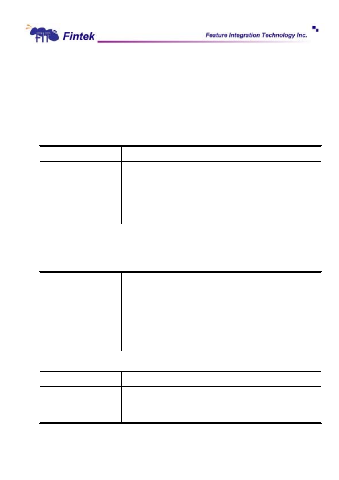
7.4 UART 2 Register
7.4.1 Logic Device Number Register
Logic Device Number Register Index 07h
Bit Name R/W Default Description
7-0 LDN R/W 00h 00h: Select FDC device configuration registers.
F71805
01h: Select UART 1 device configuration registers.
02h: Select UART 2 device configuration registers.
03h: Select Parallel Port device configuration registers.
04h: Select Hardware Monitor device configuration registers.
06h: Select GPIO device configuration registers.
0ah: Select PME device configuration registers.
Otherwise: reserved.
7.4.2 UART 2 Configuration Registers
UART IRQ Sharing Register Index 26h
Bit Name R/W Default Description
7-2 Reserved - -
1 IRQ_MODE R/W 0
0 IRQ_SHAR R/W 0
Reserved.
0: PCI IRQ sharing mode (low level).
1: ISA IRQ sharing mode (low pulse).
0: disable IRQ sharing of two UART devices.
1: enable IRQ sharing of two UART devices.
UART 2 Device Enable Register Index 30h
Bit Name R/W Default Description
7-1 Reserved - - Reserved
0 UR2_EN R/W 1 0: disable UART 2.
1: enable UART 2.
45
Dec., 2006
V0.25P
Page 48
Base Address High Register Index 60h
Bit Name R/W Default Description
7-0 BASE_ADDR_HI R/W 02h The MSB of UART 2 base address.
Base Address Low Register Index 61h
Bit Name R/W Default Description
7-0 BASE_ADDR_LO R/W F8h The LSB of UART 2 base address.
IRQ Channel Select Register Index 70h
F71805
Bit Name R/W Default Description
7-4 Reserved - - Reserved.
3-0 SELUR2IRQ R/W 3h Select the IRQ channel for UART 2.
RS485 Enable Register Index F0h
Bit Name R/W Default Description
7-5 Reserved - - Reserved.
4 RS485_EN R/W 0 0: RS232 driver.
1: RS485 driver. Auto drive RTS# low when transmitting data.
3 RXW4C_IR R/W 0 0: No reception delay when SIR is changed form TX to RX.
1: Reception delays 4 characters time when SIR is changed form TX to RX.
2 TXW4C_IR R/W 0 0: No transmission delay when SIR is changed form RX to TX.
1: Transmission delays 4 characters time when SIR is changed form RX to TX.
1-0 Reserved - - Reserved.
SIR Mode Control Register Index F1h
Bit Name R/W Default Description
7 Reserved - - Reserved.
6 Reserved - - Reserved.
5 Reserved - - Reserved.
46
Dec., 2006
V0.25P
Page 49
4-3 IRMODE R/W 00 00: disable IR function.
2 HDUPLX R/W 1 0: SIR is in full duplex mode for loopbak test. TXW4C_IR and RXW4C_IR are
1 TXINV_IR R/W 0 0: IRTX is in normal condition.
0 RXINV_IR R/W 0 0: IRRX is in normal condition.
F71805
01: disable IR function.
10: IrDA function, active pulse is 1.6uS.
11: IrDA function, active pulse is 3/16 bit time.
of no use.
1: SIR is in half duplex mode.
1: inverse the IRTX.
1: inverse the IRRX.
7.4.3 Device Registers
7.4.3.1 Receiver Buffer Register Base + 0
Bit Name R/W Default Description
7-0 RBR R 00h
The data received.
Read only when LCR[7] is 0
7.4.3.2 Transmitter Holding Register Base + 0
Bit Name R/W Default Description
7-0 THR W 00h
Data to be transmitted.
Write only when LCR[7] is 0
7.4.3.3 Divisor Latch (LSB) Base + 0
Bit Name R/W Default Description
7-0 DLL R/W 01h
Baud generator divisor low byte.
Access only when LCR[7] is 1.
7.4.3.4 Divisor Latch (MSB) Base + 1
Bit Name R/W Default Description
7-0 DLM R/W 00h
Baud generator divisor high byte.
Access only when LCR[7] is 1.
7.4.3.5 Interrupt Enable Register Base + 1
Bit Name R/W Default Description
47
Dec., 2006
V0.25P
Page 50
7-4 Reserved - - Reserved.
3 EDSSI R/W 0 Enable Modem Status Interrupt. Access only when LCR[7] is 0.
2 ELSI R/W 0 Enable Line Status Error Interrupt. Access only when LCR[7] is 0.
1 ETBFI R/W 0 Enable Transmitter Holding Register Empty Interrupt. Access only when
0 ERBFI R/W 0 Enable Received Data Available Interrupt. Access only when LCR[7] is 0.
7.4.3.6 Interrupt Identification Register Base + 2
Bit Name R/W Default Description
7 FIFO_EN R 0
6 FIFO_EN R 0
5-4 Reserved - - Reserved.
3-1 IRQ_ID R 000
0 IRQ_PENDN R 1
F71805
LCR[7] is 0.
0: FIFO is disabled
1: FIFO is enabled.
0: FIFO is disabled
1: FIFO is enabled.
000: Interrupt is caused by Modem Status
001: Interrupt is caused by Transmitter Holding Register Empty
010: Interrupt is caused by Received Data Available.
110: Interrupt is caused by Character Timeout
011: Interrupt is caused by Line Status.
1: Interrupt is not pending.
0: Interrupt is pending.
7.4.3.7 FIFO Control Register Base + 2
Bit Name R/W Default Description
7-6 RCV_TRIG W 00
5-3 Reserved - - Reserved.
2 CLRTX R 0
1 CLRRX R 0
0 FIFO_EN R 0
00: Receiver FIFO trigger level is 1.
01: Receiver FIFO trigger level is 4.
10: Receiver FIFO trigger level is 8.
11: Receiver FIFO trigger level is 14.
Reset the transmitter FIFO.
Reset the receiver FIFO.
0: Disable FIFO.
1: Enable FIFO.
7.4.3.8 Line Control Register Base + 3
Bit Name R/W Default Description
7 DLAB R/W 0
6 SETBRK R/W 0
5 STKPAR R/W 0
4 EPS R/W 0
3 PEN R/W 0
0: Divisor Latch can’t be accessed.
1: Divisor Latch can be accessed via Base and Base+1.
0: Transmitter is in normal condition.
1: Transmit a break condition.
XX0: Parity Bit is disable
001: Parity Bit is odd.
011: Parity Bit is even
101: Parity Bit is logic 1
111: Parity Bit is logic 0
48
Dec., 2006
V0.25P
Page 51
F71805
2 STB R/W 0
1-0 WLS R/W 00
0: Stop bit is one bit
1: When word length is 5 bit stop bit is 1.5 bit
else stop bit is 2 bit
00: Word length is 5 bit
01: Word length is 6 bit
10: Word length is 7 bit
11: Word length is 8 bit
7.4.3.9 MODEM Control Register Base + 4
Bit Name R/W Default Description
7-5 Reserved R/W -
4 LOOP R/W 0
3 OUT2 R/W 0
2 OUT1 R/W 0
1 RTS R/W 0
0 DTR R/W 0
Reserved.
0: UART in normal condition.
1: UART is internal loop back
0: All interrupt is disabled.
1: Interrupt is enabled(disabled) by IER.
Read from MSR[6] is loop back mode
0: RTS# is forced to logic 1
1: RTS# is forced to logic 0
0: DTR# is forced to logic 1
1: DTR# is forced to logic 0
7.4.3.10 Line Status Register Base + 5
Bit Name R/W Default Description
7 RCR_ERR R 0
6 TEMT R 1
5 THRE R 1
4 BI R 0
3 FE R 0
2 PE R 0
1 OE R 0
0 DR R 0
0: No error in the FIFO when FIFO is enabled
1: Error in the FIFO when FIFO is enabled.
0: Transmitter is in transmitting.
1: Transmitter is empty.
0: Transmitter Holding Register is not empty.
1: Transmitter Holding Register is empty.
0: No break condition detected.
1: A break condition is detected.
0: Data received has no frame error.
1: Data received has frame error.
0: Data received has no parity error.
1: Data received has parity error.
0: No overrun condition occurred.
1: An overrun condition occurred.
0: No data is ready for read.
1: Data is received.
7.4.3.11 MODEM Status Register Base + 6
Bit Name R/W Default Description
7 DCD R -
6 RI R -
5 DSR R -
Complement of DCD# input. In loop back mode, this bit is equivalent to OUT2
in MCR.
Complement of RI# input. In loop back mode , this bit is equivalent to OUT1 in
MCR
Complement of DSR# input. In loop back mode , this bit is equivalent to DTR in
MCR
49
Dec., 2006
V0.25P
Page 52
F71805
4 CTS R -
3 DDCD R 0
2 TERI R 0
1 DDSR R 0
0 DCTS R 0
Complement of CTS# input. In loop back mode , this bit is equivalent to RTS in
MCR
0: No state changed at DCD#.
1: State changed at DCD#.
0: No Trailing edge at RI#.
1: A low to high transition at RI#.
0: No state changed at DSR#.
1: State changed at DSR#.
0: No state changed at CTS#.
1: State changed at CTS#.
7.4.3.12 Scratch Register Base + 7
Bit Name R/W Default Description
7-0 SCR R/W 00h
Scratch register.
7.5 Parallel Port Register
7.5.1 Logic Device Number Register
Logic Device Number Register Index 07h
Bit Name R/W Default Description
7-0 LDN R/W 00h 00h: Select FDC device configuration registers.
01h: Select UART 1 device configuration registers.
02h: Select UART 2 device configuration registers.
03h: Select Parallel Port device configuration registers.
04h: Select Hardware Monitor device configuration registers.
06h: Select GPIO device configuration registers.
0ah: Select PME device configuration registers.
Otherwise: reserved.
7.5.2 Parallel Port Configuration Registers
Parallel Port Device Enable Register Index 30h
Bit Name R/W Default Description
7-1 Reserved - - Reserved
0 PRT_EN R/W 1 0: disable Parallel Port.
1: enable Parallel Port.
50
Dec., 2006
V0.25P
Page 53
Base Address High Register Index 60h
Bit Name R/W Default Description
7-0 BASE_ADDR_HI R/W 03h The MSB of Parallel Port base address.
Base Address Low Register Index 61h
Bit Name R/W Default Description
7-0 BASE_ADDR_LO R/W 78h The LSB of Parallel Port base address.
IRQ Channel Select Register Index 70h
Bit Name R/W Default Description
7-4 Reserved - - Reserved.
3-0 SELPRTIRQ R/W 7h Select the IRQ channel for Parallel Port.
F71805
DMA Channel Select Register Index 74h
Bit Name R/W Default Description
7-5 Reserved - 0 Reserved.
4 ECP_DMA_MODE R/W 0 0: non-burst mode DMA.
1: enable burst mode DMA.
3 Reserved - 0 Reserved.
2-0 SELPRTDMA R/W 011 Select the DMA channel for Parallel Port.
PRT Mode Select Register Index F0h
Bit Name R/W Default Description
7 Reserved - - Reserved.
6-3 ECP_FIFO_THR R/W 1000 ECP FIFO threshold.
2-0 PRT_MODE R/W 010 000: Standard and Bi-direction (SPP) mode.
001: EPP 1.9 and SPP mode.
010: ECP mode (default).
011: ECP and EPP 1.9 mode.
100: Printer mode.
101: EPP 1.7 and SPP mode.
110: Reserved.
111: ECP and EPP1.7 mode.
7.5.3 Device Registers
7.5.3.1 Parallel Port Data Register Base + 0
Bit Name R/W Default Description
7-0 DATA R/W 00h The output data to drive the parallel port data lines.
51
Dec., 2006
V0.25P
Page 54
7.5.3.2 ECP Address FIFO Register Base + 0
Bit Name R/W Default Description
7-0 ECP_AFIFO R/W 00h
F71805
Access only in ECP Parallel Port Mode and the ECP_MODE programmed in
the Extended Control Register is 011.
The data written to this register is placed in the FIFO and tagged as an
Address/RLE. It is auto transmitted by the hardware. The operation is only
defined for forward direction. It divide into two parts :
Bit 7 :
0: bits 6-0 are run length, indicating how many times the next byte to appear (0
= 1time, 1 = 2times, 2 = 3times and so on).
1: bits 6-0 are a ECP address.
Bit 6-0 :
Address or RLE depends on bit 7.
7.5.3.3 Device Status Register Base + 1
Bit Name R/W Default Description
7 BUSY_N R - Inverted version of parallel port signal BUSY.
6 ACK_N R - Version of parallel port signal ACK#.
5 PERROR R - Version of parallel port signal PE.
4 SELECT R - Version of parallel port signal SLCT.
3 ERR_N R - Version of parallel port signal ERR#.
2-1 Reserved R 11 Reserved. Return 11b when read.
0 TMOUT R - This bit is valid only in EPP mode. Return 1 when in other modes.
It indicates that a 10uS time out has occurred on the EPP bus.
0: no time out error.
1: time out error occurred, write 1 to clear.
7.5.3.4 Device Control Register Base + 2
Bit Name R/W Default Description
7-6 Reserved - 11 Reserved. Return 11b when read.
5 DIR R/W 0 0: the parallel port is in output mode.
1: the parallel port is in input mode.
It is auto reset to 0 when in SPP mode.
4 ACKIRQ_EN R/W 0 Enable an interrupt at the rising edge of ACK#.
3 SLIN R/W 0 Inverted and then drives the parallel port signal SLIN#.
When read, the status of inverted SLIN# is return.
2 INIT_N R/W 0 Drives the parallel port signal INIT#.
When read, the status of INIT# is return.
1 AFD R/W 0 Inverted and then drives the parallel port signal AFD#.
When read, the status of inverted AFD# is return.
52
Dec., 2006
V0.25P
Page 55
0 STB R/W 0 Inverted and then drives the parallel port signal STB#.
7.5.3.5 EPP Address Register Base + 3
Bit Name R/W Default Description
7 EPP_ADDR R/W 00h
7.5.3.6 EPP Data Register Base + 4 – Base + 7
Bit Name R/W Default Description
7 EPP_DATA R/W 00h
F71805
When read, the status of inverted STB# is return.
Write this register will cause the hardware to auto transmit the written data to
the device with the EPP Address Write protocol.
Read this register will cause the hardware to auto receive data from the device
by with the EPP Address Read protocol.
Write this register will cause the hardware to auto transmit the written data to
the device with the EPP Data Write protocol.
Read this register will cause the hardware to auto receive data from the device
by with the EPP Data Read protocol.
7.5.3.7 Parallel Port Data FIFO Base + 400h
Bit Name R/W Default Description
7-0 C_FIFO R/W 00h Data written to this FIFO is auto transmitted by the hardware to the device by
using standard parallel port protocol.
It is only valid in ECP and the ECP_MODE is 010b.The operation is only for
forward direction.
7.5.3.8 ECP Data FIFO Base + 400h
Bit Name R/W Default Description
7-0 ECP_DFIFO R/W 00h Data written to this FIFO when DIR is 0 is auto transmitted by the hardware to
the device by using ECP parallel port protocol.
Data is auto read from device into the FIFO when DIR is 1 by the hardware by
using ECP parallel port protocol. Read the FIFO will return the content to the
system.
It is only valid in ECP and the ECP_MODE is 011b.
7.5.3.9 ECP Test FIFO Base + 400h
Bit Name R/W Default Description
7-0 T_FIFO R/W 00h Data may be read, written from system to the FIFO in any Direction. But no
hardware handshake occurred on the parallel port lines. It could be used to test
the empty, full and threshold of the FIFO.
It is only valid in ECP and the ECP_MODE is 110b.
7.5.3.10 ECP Configuration Register A Base + 400h
Bit Name R/W Default Description
53
Dec., 2006
V0.25P
Page 56
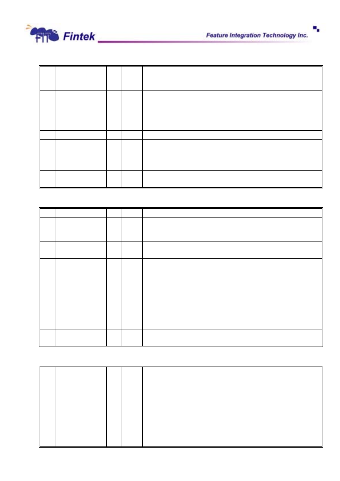
7 IRQ_MODE R 0 0: interrupt is ISA pulse.
6-4 IMPID R 001 000: the design is 16-bit implementation.
3 Reserved R - Reserved.
2 BYTETRAN_N R 1 0: when transmitting there is 1 byte waiting in the transceiver that does not
1-0 Reserved R 00 Return 00 when read.
F71805
1: interrupt is ISA level.
Only valid in ECP and ECP_MODE is 111b.
001: the design is 8-bit implementation (default).
010: the design is 32-bit implementation.
011-111: Reserved.
Only valid in ECP and ECP_MODE is 111b.
affect the FIFO full condition.
1: when transmitting the state of the full bit includes the byte being transmitted.
Only valid in ECP and ECP_MODE is 111b.
Only valid in ECP and ECP_MODE is 111b.
7.5.3.11 ECP Configuration Register B Base + 401h
Bit Name R/W Default Description
7 COMP R 0 0: only send uncompressed data.
1: compress data before sending.
Only valid in ECP and ECP_MODE is 111b.
6 Reserved R 1 Reserved. Return 1 when read.
Only valid in ECP and ECP_MODE is 111b.
5-3 ECP_IRQ_CH R 001 000: the interrupt selected with jumper.
001: select IRQ 7 (default).
010: select IRQ 9.
011: select IRQ 10.
100: select IRQ 11.
101: select IRQ 14.
110: select IRQ 15.
111: select IRQ 5.
Only valid in ECP and ECP_MODE is 111b.
2-0 ECP_DMA_CH R 011 Return the DMA channel of ECP parallel port.
Only valid in ECP and ECP_MODE is 111b.
7.5.3.12 Extended Control Register Base + 402h
Bit Name R/W Default Description
7-5 ECP_MODE R/W 000 000: SPP Mode.
001: PS/2 Parallel Port Mode.
010: Parallel Port Data FIFO Mode.
011: ECP Parallel Port Mode.
100: EPP Mode.
101: Reserved.
110: Test Mode.
111: Configuration Mode.
Only valid in ECP.
54
Dec., 2006
V0.25P
Page 57
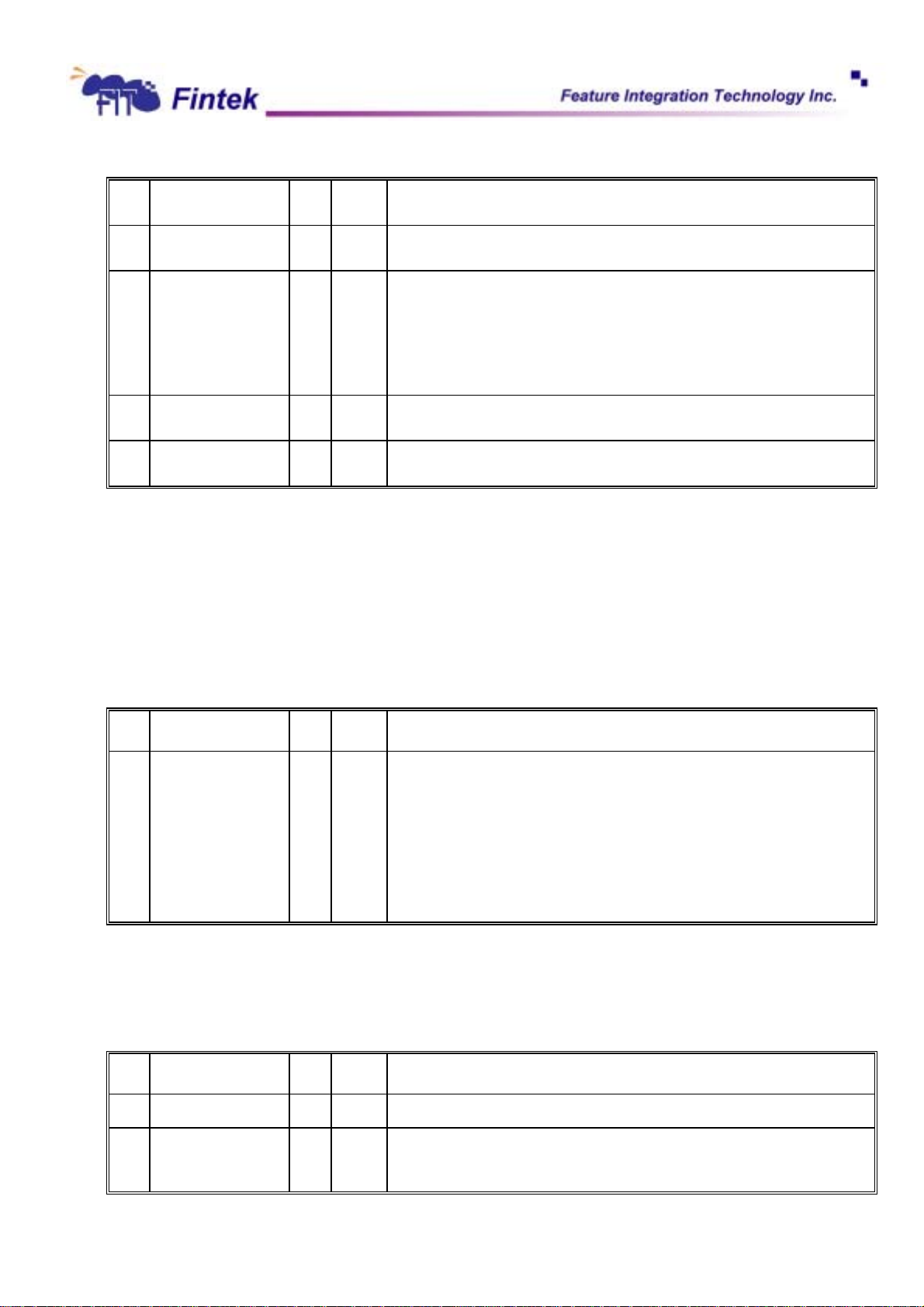
4 ERRINTR_EN R/W 0 0: disable the interrupt generated on the falling edge of ERR#.
3 DAMEN R/W 0 0: disable DMA.
2 SERVICEINTR R/W 1 0: enable the following case of interrupt.
1 FIFOFULL R 0 0: The FIFO has at least 1 free byte.
0 FIFOEMPTY R 0 0: The FIFO contains at least 1 byte.
F71805
1: enable the interrupt generated on the falling edge of ERR#.
1: enable DMA. DMA starts when SERVICEINTR is 0.
DMAEN = 1: DMA mode.
DMAEN = 0, DIR = 0: set to 1 whenever there are writeIntrThreshold or more
bytes are free in the FIFO.
DMAEN = 0, DIR = 0: set to 1 whenever there are readIntrThreshold or more
bytes are valid to be read in the FIFO.
1: The FIFO is completely full.
1: The FIFO is completely empty.
7.6 Hardware Monitor Register
7.6.1 Logic Device Number Registers
Logic Device Number Register Index 07h
Bit Name R/W Default Description
7-0 LDN R/W 00h 00h: Select FDC device configuration registers.
01h: Select UART 1 device configuration registers.
02h: Select UART 2 device configuration registers.
03h: Select Parallel Port device configuration registers.
04h: Select Hardware Monitor device configuration registers.
06h: Select GPIO device configuration registers.
0ah: Select PME device configuration registers.
Otherwise: reserved.
7.6.2 Hardware Monitor Configuration Registers
Hardware Monitor Device Enable Register Index 30h
Bit Name R/W Default Description
7-1 Reserved - - Reserved
0 HM_EN R/W 0 0: disable Hardware Monitor.
1: enable Hardware Monitor.
55
Dec., 2006
V0.25P
Page 58
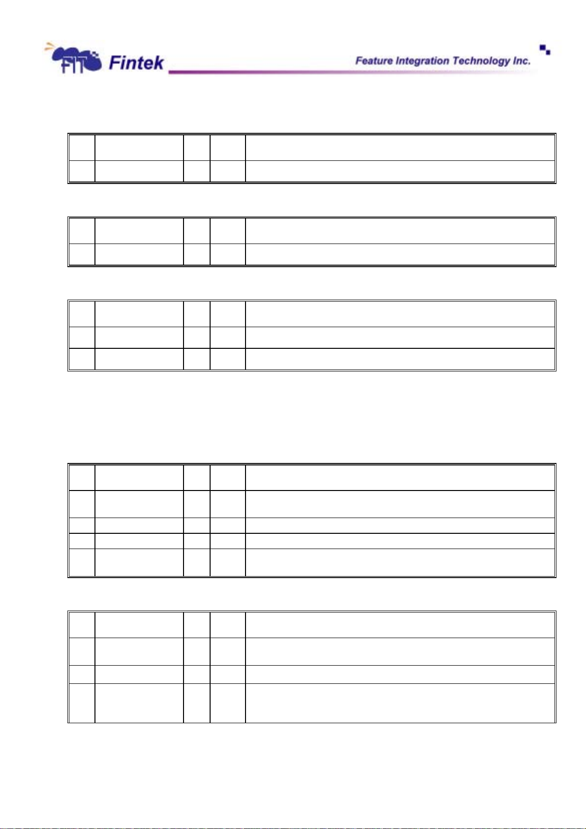
Base Address High Register Index 60h
Bit Name R/W Default Description
7-0 BASE_ADDR_HI R/W 02h The MSB of Hardware Monitor base address.
Base Address Low Register Index 61h
Bit Name R/W Default Description
7-0 BASE_ADDR_LO R/W 95h The LSB of Hardware Monitor base address.
IRQ Channel Select Register Index 70h
F71805
Bit Name R/W Default Description
7-4 Reserved - - Reserved.
3-0 SELHMIRQ R/W 0h Select the IRQ channel for Hardware Monitor.
7.6.3 Device Registers
7.6.3.1 START_STOP Control Register Index 00h
Bit Name R/W Default Description
7 INIT R/W 0 Set one restores power on default value to all registers. This bit clears itself
since the power on default is zero.
6 SOFT_PWDN R/W 0 Set this bit to 1 will power down A/D converter circuit. Default is 0.
5-1 Reserved R - Read back will be 0.
0 START R/W 1 A one enables startup of monitoring operations; a zero puts the part in standby
mode.
7.6.3.2 Temperature Mode Control Register Index 01h
Bit Name R/W Default Description
7-6 Temperature
Fault Queue
5-4 Reserved R -
3 COMB_LEVEL R/W 1
R/W 00
This value stands for how many times of successive temperature fault can be
tolerated. 00: 1 times. 01: 2 times. 10: 4 times. 11: 8 times.
Read back data will be “0”.
Set to 1, enable COMB filter. Set to 0, disable COMB filter.
COMB filter is only applied to BJT thermal diode mode.
If temperature select thermistor mode, the COMB filter will not work on it.
56
Dec., 2006
V0.25P
Page 59
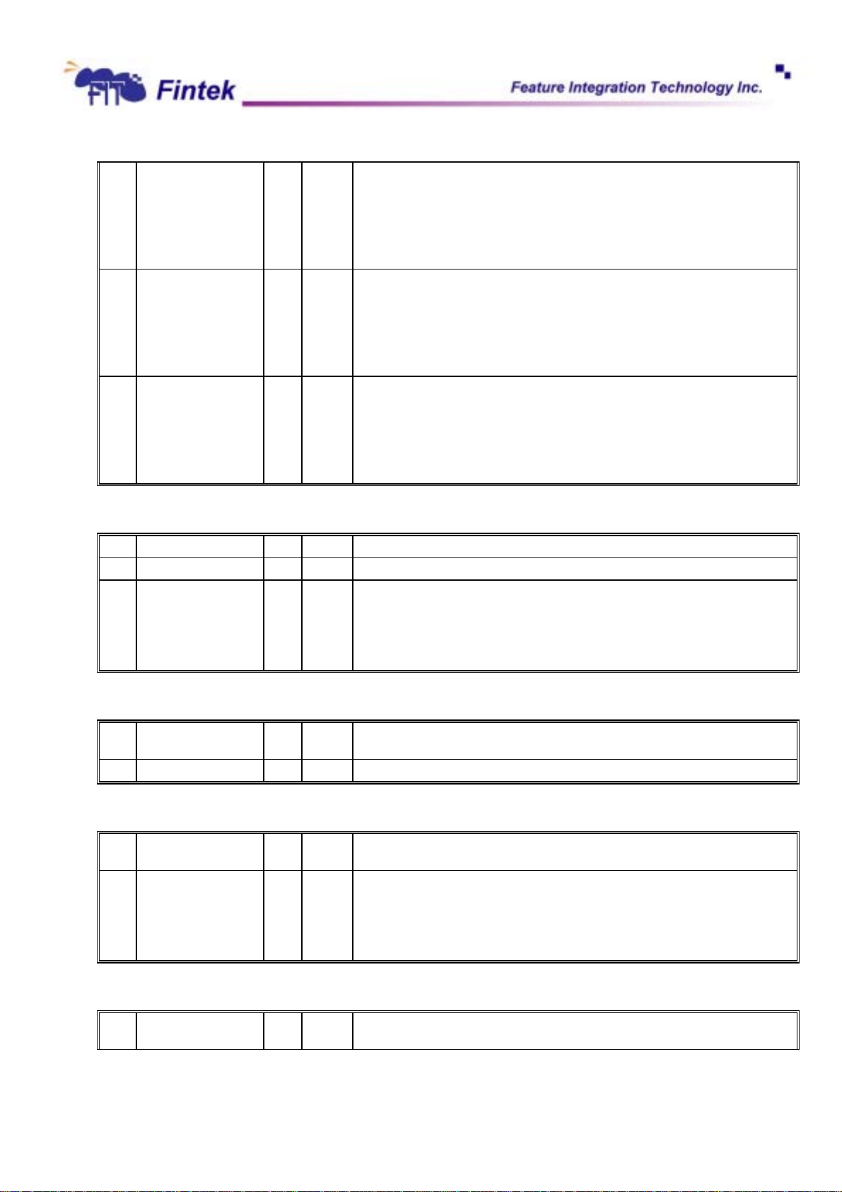
F71805
2 T3_MODE R/W 0
1 T2_MODE R/W 0
0 T1_MODE R/W 0
Set to 1, select T3 as connected to a BJT thermal diode. At this mode, T3
detected temperature ranges from 0°C ~ 140°C, not considering the
T3OFFSET(index 92h) effect.
Set to 0, select T3 as connected to a thermistor. At this mode, T3 detected
temperature ranges from 0°C ~ 127°C, not considering the T3OFFSET(index
92h) effect.
Set to 1, select T2 as connected to a BJT thermal diode. At this mode, T2
detected temperature ranges from 0°C ~ 140°C, not considering the
T2OFFSET(index 91h) effect.
Set to 0, select T2 as connected to a thermistor. At this mode, T2 detected
temperature ranges from 0°C ~ 127°C, not considering the T2OFFSET(index
91h) effect.
Set to 1, select T1 as connected to a BJT thermal diode. At this mode, T1
detected temperature ranges from 0°C ~ 140°C, not considering the
T1OFFSET(index 90h) effect.
Set to 0, select T1 as connected to a thermistor. At this mode, T1 detected
temperature ranges from 0°C ~ 127°C, not considering the T1OFFSET(index
90h) effect.
7.6.3.3 ADC_CLK Frequency Control Register Index 02h
Bit Name R/W Default Description
7-2 Reserved R/W -
1-0 ADC_CLK_SEL R/W 00
Select ADC clock frequency.
00 : 12.8K(Default)
01 : 6.4K
10 : 3.2K
11 : 1.6K
7.6.3.4 External BJT Offset Register Index 09h
Bit Name R/W Default Description
7-0 Reserved R/W 37h
7.6.3.5 FAN1 Full Speed Count Register 0 Index 0Ah
Bit Name R/W Default Description
7-0 F1_FULL(MSB) R 0Fh When power on, the FANPWM1 will output full duty cycle (FFh) to enable
system FAN. After 10 seconds when detecting FANIN signal, assuming the
fan has been fully turned on, the fan speed count detected will be recorded in
the register. If there is no signal on FANIN after power on, the PWMOUT1 will
keep outputting FFh duty cycle.
7.6.3.6 FAN1 Full speed Count Register 1 Index 0Bh
Bit Name R/W Default Description
57
Dec., 2006
V0.25P
Page 60
7-0 F1_FULL(LSB) R FFh When power on, the FANPWM1 will output full duty cycle (FFh) to enable
7.6.3.7 FAN2 Full Speed Count Register 0 Index 0Ch
Bit Name R/W Default Description
7-0 F2_FULL(MSB) R 0Fh When power on, the FANPWM2 will output full duty cycle (FFh) to enable
F71805
system FAN. After 10 seconds when detecting FANIN signal, assuming the
fan has been fully turned on, the fan speed count detected will be recorded in
the register. If there is no signal on FANIN after power on, the PWMOUT1 will
keep outputting FFh duty cycle.
system FAN. After 10 seconds when detecting FANIN signal, assuming the
fan has been fully turned on, the fan speed count detected will be recorded in
the register. If there is no signal on FANIN2 after power on, the PWMOUT2 will
keep outputting FFh duty cycle.
7.6.3.8 FAN2 Full speed Count Register 1 Index 0Dh
Bit Name R/W Default Description
7-0 F2_FULL(LSB) R FFh When power on, the FANPWM2 will output full duty cycle (FFh) to enable
system FAN. After 10 seconds when detecting FANIN signal, assuming the
fan has been fully turned on, the fan speed count detected will be recorded in
the register. If there is no signal on FANIN1 after power on, the PWMOUT2 will
keep outputting FFh duty cycle.
7.6.3.9 FAN3 Full Speed Count Register 0 Index 0Eh
Bit Name R/W Default Description
7-0 F3_FULL(MSB) R 0Fh When power on, the FANPWM3 will output full duty cycle (FFh) to enable
system FAN. After 10 seconds when detecting FANIN signal, assuming the
fan has been fully turned on, the fan speed count detected will be recorded in
the register. If there is no signal on FANIN2 after power on, the PWMOUT3 will
keep outputting FFh duty cycle.
7.6.3.10 FAN3 Full speed Count Register 1 Index 0Fh
Bit Name R/W Default Description
7-0 F3_FULL(LSB) R FFh When power on, the FANPWM3 will output full duty cycle (FFh) to enable
system FAN. After 10 seconds when detecting FANIN signal, assuming the
fan has been fully turned on, the fan speed count detected will be recorded in
the register. If there is no signal on FANIN3 after power on, the PWMOUT3 will
keep outputting FFh duty cycle.
7.6.3.11 Value RAM Index 10h - 2Fh, 40h - 59h
In the following table, the unit of voltage reading/limit is 8mV. The unit of temperature reading/limit is 1ºC.
Address 10-3F R/W Description
0Ah RO FAN1 full speed count reading [11:8]
58
Dec., 2006
V0.25P
Page 61
F71805
0Bh RO FAN1 full speed count reading [7:0]
0Ch RO FAN2 full speed count reading [11:8]
0Dh RO FAN2 full speed count reading [7:0]
0Eh RO FAN3 full speed count reading [11:8]
0Fh RO FAN3 full speed count reading [7:0]
10h RO VCC reading. This reading is the divided voltage of VCC inside the chip.
11h RO VIN1 reading.
12h RO VIN2 reading.
13h RO VIN3 reading.
14h RO VIN4 reading.
15h RO VIN5 reading.
16h RO VIN6 reading.
17h RO VIN7 reading.
18h RO VIN8 reading.
19h Reserved
1Ah Reserved
1Bh RO T1 temperature reading.
1Ch RO T2 temperature reading.
1Dh RO T3 temperature reading.
1Eh Reserved
20h RO FAN1 count reading (MSB)
21h RO FAN1 count reading (LSB)
22h RO FAN2 count reading (MSB)
23h RO FAN2 count reading (LSB)
24h RO FAN3 count reading (MSB)
25h RO FAN3 count reading (LSB)
26h ~ 27h Reserved
28h R/W FAN1 count limit. (MSB)
29h R/W FAN1 count limit. (LSB)
2Ah R/W FAN2 count limit. (MSB)
2Bh R/W FAN2 count limit. (LSB).
2Ch R/W FAN3 count limit. (MSB)
2Dh R/W FAN3 count limit. (LSB)
2Eh Reserved
2Fh Reserved
40h R/W VCC high limit. This limit should correspond to the divided voltage.
41h R/W VCC low limit. This limit should correspond to the divided voltage.
42h R/W VIN1 high limit.
43h R/W VIN1 low limit.
44h R/W VIN2 high limit.
45h R/W VIN2 low limit.
46h R/W VIN3 high limit.
47h R/W VIN3 low limit.
48h R/W VIN4 high limit.
49h R/W VIN4 low limit.
4Ah R/W VIN5 high limit.
4Bh R/W VIN5 low limit.
4Ch R/W VIN6 high limit.
4Dh R/W VIN6 low limit.
4Eh R/W VIN7 high limit.
4Fh R/W VIN7 low limit.
50h R/W VIN8 high limit.
59
Dec., 2006
V0.25P
Page 62
7.6.3.12 INTERRUPT ENABLE Control Register 1 Index 30h
Bit Name R/W Default Description
7 EN_VIN7 R/W 0 Set to 1, enables VIN7 abnormal interrupt.
6 EN_VIN6 R/W 0 Set to 1, enables VIN6 abnormal interrupt.
5 EN_VIN5 R/W 0 Set to 1, enables VIN5 abnormal interrupt.
4 EN_VIN4 R/W 0 Set to 1, enables VIN4 abnormal interrupt.
3 EN_VIN3 R/W 0 Set to 1, enables VIN3 abnormal interrupt.
2 EN_VIN2 R/W 0 Set to 1, enables VIN2 abnormal interrupt.
1 EN_VIN1 R/W 0 Set to 1, enables VIN1 abnormal interrupt.
0 EN_3VDD R/W 0 Set to 1, enables 3VDD abnormal interrupt.
F71805
51h R/W VIN8 low limit.
52h Reserved
53h Reserved
54h R/W T1 high limit.
55h R/W T1 low limit.
56h R/W T2 high limit.
57h R/W T2 low limit.
58h R/W T3 high limit.
59h R/W T3 low limit.
7.6.3.13 INTERRUPT ENABLE Control Register 2 Index 31h
Bit Name R/W Default Description
7-6 Reserved - - Reserved.
5 EN_T3 R/W 0 Set to 1, enables T3 abnormal interrupt.
4 EN_T2 R/W 0 Set to 1, enables T2 abnormal interrupt.
3 EN_T1 R/W 0 Set to 1, enables T1 abnormal interrupt.
2 Reserved - - Reserved.
1 Reserved - - Reserved.
0 EN_VIN8 R/W 0 Set to 1, enables VIN8 abnormal interrupt.
7.6.3.14 INTERRUPT ENABLE Control Register 3 Index 32h
Bit Name R/W Default Description
7 Reserved - - Reserved.
6 Reserved - - Reserved.
5 EN_FAN3_TAR R/W 0 Set to 1, enables FAN3 target speed mismatched interrupt when FANPWM3
duty-cycle is 100%.
4 EN_FAN2_TAR R/W 0 Set to 1, enables FAN2 target speed mismatched interrupt when FANPWM2
duty-cycle is 100%.
3 EN_FAN1_TAR R/W 0
2 EN_FAN3_LMT R/W 0
Set to 1, enables FAN1 target speed mismatched interrupt when FANPWM1
duty-cycle is 100%.
Set to 1, enables FAN3 abnormal interrupt.
60
Dec., 2006
V0.25P
Page 63
1 EN_FAN2_LMT R/W 0 Set to 1, enables FAN2 abnormal interrupt.
0 EN_FAN1_LMT R/W 0 Set to 1, enables FAN1 abnormal interrupt.
7.6.3.15 INTERRUPT STATUS Register 1 Index 33h
Bit Name R/W Default Description
7 VIN7_STS R/W 0 A one indicates VIN7 reaches its high or low limit. Write 1 to clear this bit,
6 VIN6_STS R/W 0 A one indicates VIN6 reaches its high or low limit. Write 1 to clear this bit,
5 VIN5_STS R/W 0 A one indicates VIN5 reaches its high or low limit. Write 1 to clear this bit,
4 VIN4_STS R/W 0 A one indicates VIN4 reaches its high or low limit. Write 1 to clear this bit,
3 VIN3_STS R/W 0
2 VIN2_STS R/W 0
1 VIN1_STS R/W 0 A one indicates VIN1 reaches its high or low limit. Write 1 to clear this bit,
0 3VDD_STS R/W 0 A one indicates 3VDD reaches its high or low limit. Write 1 to clear this bit,
F71805
write 0 will be ignored.
write 0 will be ignored.
write 0 will be ignored.
write 0 will be ignored.
A one indicates VIN3 reaches its high or low limit. Write 1 to clear this bit,
write 0 will be ignored.
A one indicates VIN2 reaches its high or low limit. Write 1 to clear this bit,
write 0 will be ignored.
write 0 will be ignored.
write 0 will be ignored.
7.6.3.16 INTERRUPT STATUS Register 2 Index 34h
Bit Name R/W Default Description
7-6 Reserved - - Reserved.
5 T3_STS R/W 0 A one indicates T3 reaches its high or low limit. Write 1 to clear this bit, write
0 will be ignored.
4 T2_STS R/W 0 A one indicates T2 reaches its high or low limit. Write 1 to clear this bit, write
0 will be ignored.
3 T1_STS R/W 0
2 Reserved - -
1 Reserved - - Reserved.
0 VIN8_STS R/W 0 A one indicates VIN8 reaches its high or low limit. Write 1 to clear this bit,
A one indicates T1 reaches its high or low limit. Write 1 to clear this bit, write
0 will be ignored.
Reserved.
write 0 will be ignored.
7.6.3.17 INTERRUPT STATUS Register 3 Index 35h
Bit Name R/W Default Description
7 Reserved - - Reserved.
6 Reserved - -
Reserved.
5 FAN3_TAR_STS R/W 0 A one indicates FAN3 can not reach the expect count in time. The time is
defined by FAN3 Fault Time registers.
61
Dec., 2006
V0.25P
Page 64
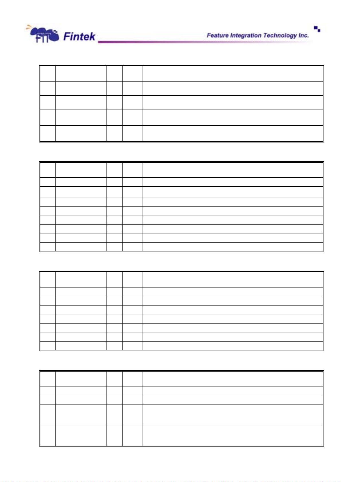
4 FAN2_TAR_STS R/W 0 A one indicates FAN2 can not reach the expect count in time. The time is
3 FAN1_TAR_STS R/W 0
2 FAN3_STS R/W 0
1 FAN2_STS R/W 0 A one indicates FAN2 reaches its high or low limit. Write 1 to clear this bit,
0 FAN1_STS R/W 0 A one indicates FAN1 reaches its high or low limit. Write 1 to clear this bit,
7.6.3.18 REAL_TIME STATUS Register 1 Index 36h
Bit Name R/W Default Description
F71805
defined by FAN2 Fault Time registers.
A one indicates FAN1 can not reach the expect count in time. The time is
defined by FAN1 Fault Time registers.
A one indicates FAN3 reaches its high or low limit. Write 1 to clear this bit,
write 0 will be ignored.
write 0 will be ignored.
write 0 will be ignored.
7 VIN7_RT R 0 A one indicates VIN7 is at abnormal range.
6 VIN6_RT R 0
5 VIN5_RT R 0 A one indicates VIN5 is at abnormal range.
4 VIN4_RT R 0 A one indicates VIN4 is at abnormal range.
3 VIN3_RT R 0
2 VIN2_RT R 0
1 VIN1_RT R 0 A one indicates VIN1 is at abnormal range.
0 3VDD_RT R 0 A one indicates 3VDD is at abnormal range.
A one indicates VIN6 is at abnormal range.
A one indicates VIN3 is at abnormal range.
A one indicates VIN2 is at abnormal range.
7.6.3.19 REAL_TIME STATUS Register 2 Index 37h
Bit Name R/W Default Description
7-6 Reserved - - Reserved.
5 T3_RT R 0 A one indicates T3 exceeds its high limit.
4 T2_RT R 0 A one indicates T2 exceeds its high limit.
3 T1_RT R 0
2 Reserved - -
1 Reserved - - Reserved.
0 VIN8_RT R 0 A one indicates VIN8 exceeds its high limit.
A one indicates T1 exceeds its high limit.
Reserved.
7.6.3.20 REAL_TIME STATUS Register 3 Index 38h
Bit Name R/W Default Description
7 Reserved - - Reserved.
6 Reserved - - Reserved.
5 FAN3_TAR_RT R 0
4 FAN2_TAR_RT R 0
A one indicates FAN3 can not reach the expect count in time when FANPWM3
duty-cycle is 100%. The time is defined by FAN3 Fault Time registers. After
FAN3 reaches the expect count, the bit will be set to 0.
A one indicates FAN2 can not reach the expect count in time when FANPWM2
duty-cycle is 100%. The time is defined by FAN2 Fault Time registers. After
FAN2 reaches the expect count, the bit will be set to 0.
62
Dec., 2006
V0.25P
Page 65
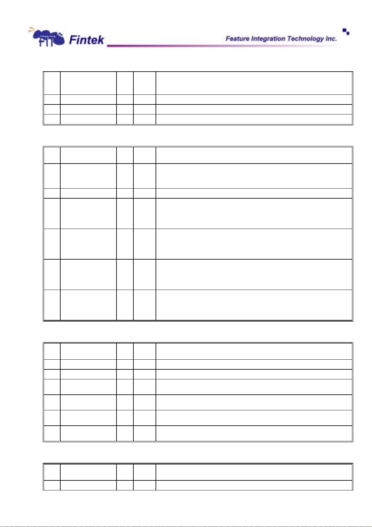
F71805
3 FAN1_TAR_RT R 0
2 FAN3_RT R 0
1 FAN2_RT R 0 A one indicates FAN2 is at abnormal range.
0 FAN1_RT R 0 A one indicates FAN1 is at abnormal range.
A one indicates FAN1 can not reach the expect count in time when FANPWM1
duty-cycle is 100%. The time is defined by FAN1 Fault Time registers. After
FAN1 reaches the expect count, the bit will be set to 0.
A one indicates FAN3 is at abnormal range.
7.6.3.21 VIN_FAULT Mode Register 3 Index 39h
Bit Name R/W Default Description
7 VIN7F_SEL R/W 0 Set to 1, VIN7_ID value will not change until REG 3Ah Bit7 is cleared if that bit
is set. Set to 0, VIN7_ID value changes dynamically according to current
voltage which falls on which segments (REGD0h ~ REGD6h).
6-4 Reserved - - Reserved.
3 VIN4F_SEL R 0
2 VIN3F_SEL R 0
1 VIN2F_SEL R 0
0 VIN1F_SEL R 0
Set to 1, once VIN4_FAULT is asserted, it will not be de-asserted when VIN4 is
back to normal range.
Set to 0, VIN4_FAULT is asserted/de-asserted according to its value whether is
out of high/low limit.
Set to 1, once VIN3_FAULT is asserted, it will not be de-asserted when VIN4 is
back to normal range.
Set to 0, VIN3_FAULT is asserted/de-asserted according to its value whether is
out of high/low limit.
Set to 1, once VIN2_FAULT is asserted, it will not be de-asserted when VIN4 is
back to normal range.
Set to 0, VIN2_FAULT is asserted/de-asserted according to its value whether is
out of high/low limit.
Set to 1, once VIN1_FAULT is asserted, it will not be de-asserted when VIN4 is
back to normal range.
Set to 0, VIN1_FAULT is asserted/de-asserted according to its value whether is
out of high/low limit.
7.6.3.22 VIN_FAULT STATUS Register Index 3Ah
Bit Name R/W Default Description
7 STS_VIN7_CHG R/W 0 Read one indicates that the VIN7_ID is changed. Write 1 to clear this status.
6-4 Reserved - - Reserved.
3 STS_VIN4_FAULT R/W 0
2 STS_VIN3_FAULT R/W 0
1 STS_VIN2FAULT R/W 0
0 STS_VIN1_FAULT R/W 0
Read one indicates that VIN4 is out of its high/low limit. Write 1 to clear this
status.
Read one indicates that VIN3 is out of its high/low limit. Write 1 to clear this
status.
Read one indicates that VIN2 is out of its high/low limit. Write 1 to clear this
status.
Read one indicates that VIN1 is out of its high/low limit. Write 1 to clear this
status.
7.6.3.23 T_FAULT Control Register Index 3Bh
Bit Name R/W Default Description
7-3 Reserved - - Reserved.
63
Dec., 2006
V0.25P
Page 66
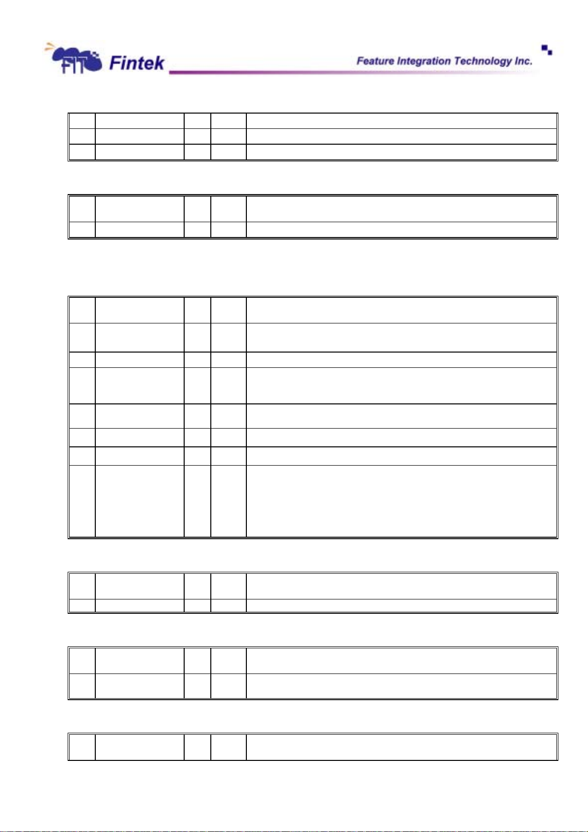
F71805
2 EN_T3_FAULT R/W 0
1 EN_T2_FAULT R/W 0
0 EN_T1_FAULT R/W 0 Set to 1, enable temperature 1(VT1) fault through pin OVT_N.
Set to 1, enable temperature 3(VT3)fault through pin OVT_N.
Set to 1, enable temperature 2(VT2) fault through pin OVT_N.
7.6.3.24 Reserved Register Index 3Ch
Bit Name R/W Default Description
7-0 Reserved - - Reserved.
7.6.3.25 FAN1 OPERATING Control Register -- Index 60h
Bit Name R/W Default Description
7 FAN1_SKIP R - When this bit is set to 1, FAN1 is not monitored.
When this bit is set to 0, FAN1 is monitored.
6 Reserved - - Reserved.
FAN1_FORCE_MONI
5
TOR
FAN1_DC_MODE
4
3
F1_LATCH_FULL
2
F1_KEEP_STOP
1-0
F1_MODE
R/W 0
R/W 0
R/W 0
R/W 0
R/W 00
Set to 1, FAN1 speed is monitored every monitor cycle even the fan is
stopped. Set to 0, FAN1 speed will not be monitored at the next monitor cycle
if the fan is stopped.
Set to 1, FAN1 control is set to DC mode.
Set to 0, FAN1 control is set to PWM duty-cycle mode.
Set to 1, current FAN1 COUNT will be bypass to FAN1_FULL_SPEED.
Set to 1, keep FANPWM1 duty-cycle decrease to STOP DUTY and hold.
00: FAN1 operates in SPEED mode. FANPWM duty-cycle is automatically
adjusted according to FAN EXPECT register.
01: FAN1 operates in TEMPERATURE mode. FANPWM duty-cycle is
automatically adjusted according to current temperature,
1x: FAN1 operates in MANUAL mode. Software set the FANPWM
duty-cycle directly.
7.6.3.26 FANPWM1 START UP DUTY-CYCLE Index 61h
Bit Name R/W Default Description
7-0
F1_START_DUTY[9:2]
R/W 30h FANPWM1 will increasing duty-cycle from 0 to this valuedirectly.
7.6.3.27 FANPWM1 STOP DUTY-CYCLE Index 62h
Bit Name R/W Default Description
7-0
F1_STOP_DUTY[9:2]
R/W 25h FANPWM1 will decreasing duty-cycle to 0 from this value directly or keep
duty-cycle in this value when FAN1_KEEP_STOP set to 1.
7.6.3.28 FANPWM1 Output Frequency Control Index 63h
Bit Name R/W Default Description
64
Dec., 2006
V0.25P
Page 67
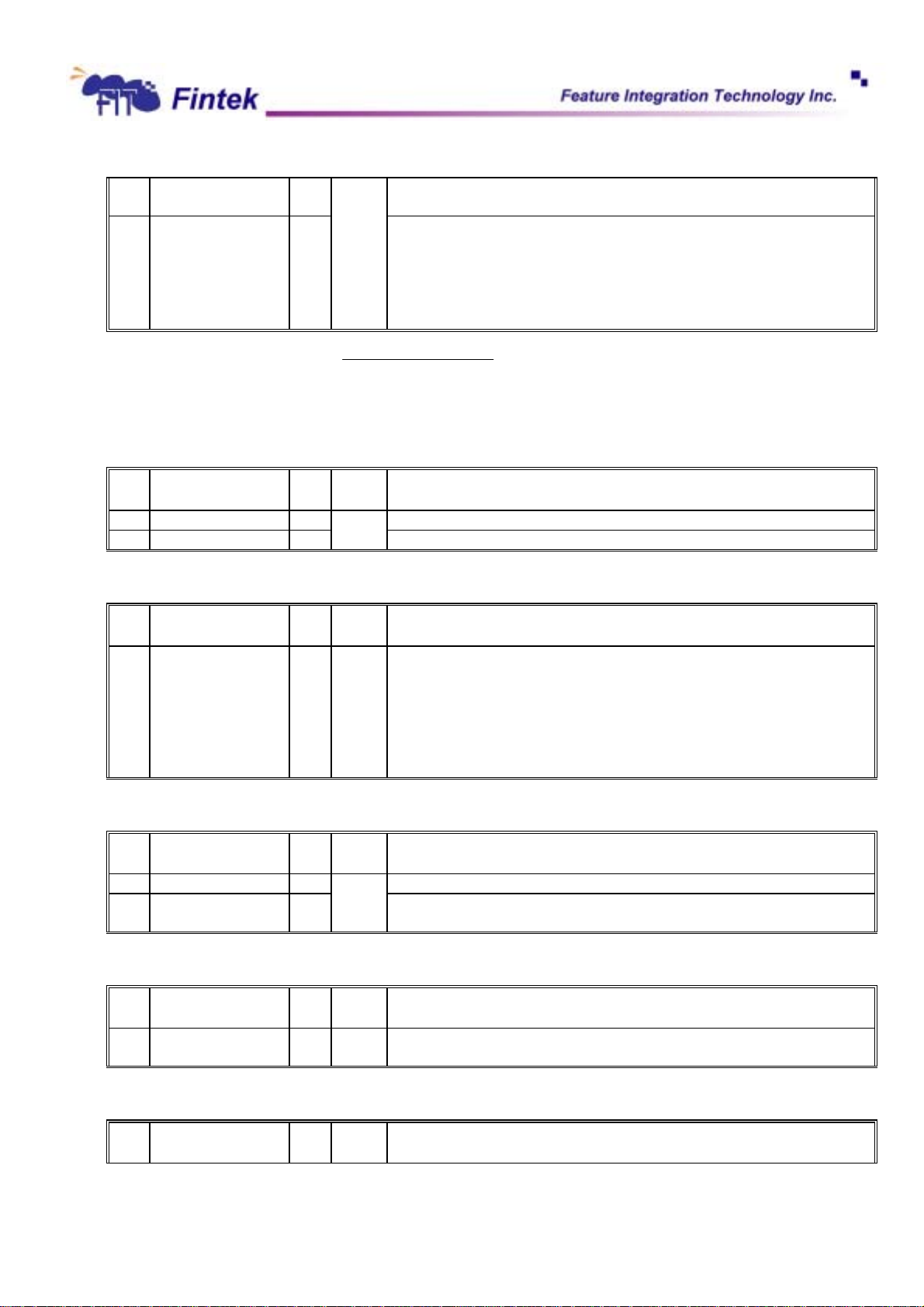
F71805
7 PWM1_DIV[7] R/W Set to 1, PRECLK(Pre-Clock) = 48M Hz ;
6-0 PWM1_DIV[6:0] R/W
FANPWM1 output frequency =
80h
Set to 0, PRECLK = 1M Hz .
Pre-divisor of PRECLK.
Set the value to 0 Pre-divisor =1
Set the value to 1 Pre-divisor =1
Set the value to 2 Pre-divisor =2
Set the value to 3 Pre-divisor =3
……………….
PRECLK
256)-(Pr ∗divisore
So, PWM frequency ranges from 30.5Hz~ 187.5KHz
7.6.3.29 FANPWM1 STEP Control Register -- Index 64h
Bit Name R/W Default Description
7-4 F1_UP_STEP R/W This value determines the increasing speed of PWM1_DUTY.
3-0 F1_DOWN_STEP R/W
00h
This value determines the decreasing speed of PWM1_DUTY.
7.6.3.30 FAN1_FAULT TIME Register Index 65h
Bit Name R/W Default Description
7-0 F1_FAULT_TIME R/W 03h This register determines the time for fan to chase to the expect speed. Two
conditions cause fan fault event:
(1). When PWM_Duty reaches FFh, if the fan speed count can’t reach the
fan expect count in the time.
(2). When PWM_Duty reaches 00h, if the fan speed count can’t reach the
fan expect count in the time.
The unit of this register is 1 second. The default value is 3 seconds.
7.6.3.31 FAN1 Expect count Register---Index 69h
Bit Name R/W Default Description
7-4 Reserved -
3-0
F1_EXPECT (MSB)
R
00h
User expect fan1 count value, program this register to control the expect
fan1 speed
7.6.3.32 FAN1 Expect count Register-- Index 6Ah
PBit Name R/W Default Description
7-0 F1_EXPECT (LSB) R 00h User expect fan1 count value, program this register to control the expect fan1
speed.
7.6.3.33 FAN1 PWM_DUTY -- Index 6Bh
Bit Name R/W Default Description
65
Dec., 2006
V0.25P
Page 68
7-0 PWM_DUTY1 R/W FFh When FAN1 control is at PWM Duty-cycle mode, this value represents the
7.6.3.34 FAN2 OPERATING Control Register -- Index 70h
Bit Name R/W Default Description
7 FAN2_SKIP R - When this bit is set to 1, FAN2 is not monitored.
6 Reserved - - Reserved.
FAN2_FORCE_MONI
5
TOR
FAN2_DC_MODE
4
3 F2_LATCH_FULL R/W 0 Set to 1, current FAN2 COUNT will be bypass to F2_FULL_SPEED.
2 F2_KEEP_STOP R/W 0 Set to 1, keep FANPWM2 duty-cycle decrease to STOP DUTY and hold.
1-0 F2_MODE R/W 00 00: FAN2 operates in SPEED mode. FANPWM duty-cycle is automatically
R/W 0
R/W 0
F71805
duty-cycle.
When FAN1 control is at DC mode, this value represents the DC voltage
output. Each step (LSB) is VCC / 256.
This register is programmable at Manual mode.
At SPEED or TEMPERATURE mode, this register reflects current
FANPWM1 duty-cycle.
When this bit is set to 0, FAN2 is monitored.
Set to 1, FAN2 speed is monitored every monitor cycle even the fan is
stopped. Set to 0, FAN2 speed will not be monitored at the next monitor cycle if
the fan is stopped.
Set to 1, FAN2 control is set to DC mode.
Set to 0, FAN2 control is set to PWM duty-cycle mode.
adjusted according to FAN EXPECT register.
01: FAN2 operates in TEMPERATURE mode. FANPWM duty-cycle is
automatically adjusted according to current temperature,
1x: FAN2 operates in MANUAL mode. Software set the FANPWM duty-cycle
directly.
7.6.3.35 FANPWM2 START UP DUTY-CYCLE Index 71h
Bit Name R/W Default Description
7-0 F2_START_DUTY R/W 30h FANPWM2 will increase duty-cycle from 0 to this value directly.
7.6.3.36 FANPWM2 STOP DUTY-CYCLE Index 72h
Bit Name R/W Default Description
7-0 F2_STOP_DUTY R/W 25h FANPWM2 will decreasing duty-cycle to 0 from this value directly or keep
duty-cycle in this value when F2_KEEP_STOP set to 1.
7.6.3.37 FANPWM2 Output Frequency Control Index 73h
Bit Name R/W Default Description
7 PWM2_DIV[7] R/W 80h Set to 1, PRECLK(Pre-Clock) = 48M Hz ;
Set to 0, PRECLK = 1M Hz .
66
Dec., 2006
V0.25P
Page 69
6-0 PWM2_DIV[6:0] R/W Pre-divisor of PRECLK.
F71805
Set the value to 0 Pre-divisor =1
Set the value to 1 Pre-divisor =1
Set the value to 2 Pre-divisor =2
Set the value to 3 Pre-divisor =3
……………….
FANPWM2 output frequency =
PRECLK
256)(Pr ∗− divisore
So, PWM frequency ranges from 30.5Hz~ 187.5KHz
7.6.3.38 FANPWM2 STEP Control Register -- Index 74h
Bit Name R/W Default Description
7-4
2_UP_STEP R/W This value determines the increasing speed of PWM2_DUTY.
3-0
2_DOWN_STEP R/W
00h
This value determines the decreasing speed of PWM2_DUTY
7.6.3.39 FAN2_FAULT TIME Register Index 75h
Bit Name R/W Default Description
7-0 F2_FAULT_TIME R/W 03h This register determines the time for fan to chase to the expect speed. Two
conditions cause fan fault event:
(1). When PWM_Duty reaches FFh, if the fan speed count can’t reach the fan
expect count in the time.
(2). When PWM_Duty reaches 00h, if the fan speed count can’t reach the fan
expect count in the time.
The unit of this register is 1 second. The default value is 180 seconds.
7.6.3.40 FAN2 Expect count Register-- Index 79h
Bit Name R/W Default Description
7-4 Reserved - Reserved.
3-0
F2_EXPECT (MSB)
R
00h
User expect fan2 count value, program this register to control the expect fan2
speed
7.6.3.41 FAN2 Expect count Register-- Index 7Ah
Bit Name R/W Default Description
7-0 F2_EXPECT (LSB) R 00h User expect fan2 count value, program this register to control the expect
fan2 speed.
7.6.3.42 FAN2 PWM_DUTY -- Index 7Bh
Bit Name R/W Default Description
67
Dec., 2006
V0.25P
Page 70
7-0 PWM_DUTY2 R/W FFh When FAN2 control is at PWM Duty-cycle mode, this value represents the
7.6.3.43 FAN3 OPERATING Control Register -- Index 80h
Bit Name R/W Default Description
7 FAN3_SKIP R - When this bit is set to 1, FAN3 is not monitored.
6 Reserved - - Reserved.
FAN3_FORCE_MONI
5
TOR
FAN3_DC_MODE
4
3 F3_LATCH_FULL R/W 0 Set to 1, current FAN3 COUNT will be bypass to F3_FULL_SPEED.
2 F3_KEEP_STOP R/W 0 Set to 1, keep FANPWM3 duty-cycle decrease to STOP DUTY and hold.
1-0 F3_MODE R/W 00 00: FAN3 operates in SPEED mode. FANPWM3 duty-cycle is
R/W 0
R/W 0
F71805
duty-cycle.
When FAN2 control is at DC mode, this value represents the DC voltage
output. Each step (LSB) is VCC / 256.
This register is programmable at Manual mode.
At SPEED or TEMPERATURE mode, this register reflects current
FANPWM1 duty-cycle.
When this bit is set to 0, FAN3 is monitored.
Set to 1, FAN3 speed is monitored every monitor cycle even the fan is
stopped. Set to 0, FAN3 speed will not be monitored at the next monitor cycle if
the fan is stopped.
Set to 1, FAN3 control is set to DC mode.
Set to 0, FAN3 control is set to PWM duty-cycle mode.
automatically adjusted according to FAN EXPECT register.
01: FAN3 operates in TEMPERATURE mode. FANPWM3 duty-cycle is
automatically adjusted according to current temperature,
1x: FAN3 operates in MANUAL mode. Software set the FANPWM3
duty-cycle directly.
7.6.3.44 FANPWM3 START UP DUTY-CYCLE Index 81h
Bit Name R/W Default Description
7-0 F3_START_DUTY R/W 30h FANPWM3 will increase duty-cycle from 0 to this value directly.
7.6.3.45 FANPWM3 STOP DUTY-CYCLE Index 82h
Bit Name R/W Default Description
7-0 F3_STOP_DUTY R/W 25h FANPWM3 will decreasing duty-cycle to 0 from this value directly or keep
duty-cycle in this value when F3_KEEP_STOP set to 1.
7.6.3.46 FANPWM3 Output Frequency Control Index 83h
Bit Name R/W Default Description
7 PWM3_DIV[7] R/W 80h Set to 1, PRECLK(Pre-Clock) = 48M Hz ;
Set to 0, PRECLK = 1M Hz .
68
Dec., 2006
V0.25P
Page 71
6-0 PWM3_DIV[6:0] R/W Pre-divisor of PRECLK.
F71805
Set the value to 0 Pre-divisor =1
Set the value to 1 Pre-divisor =1
Set the value to 2 Pre-divisor =2
Set the value to 3 Pre-divisor =3
……………….
FANPWM3 output frequency =
PRECLK
256)(Pr ∗− divisore
So, PWM frequency ranges from 30.5Hz~ 187.5KHz
7.6.3.47 FANPWM3 STEP Control Register -- Index 84h
Bit Name R/W Default Description
7-4 F3_UP_STEP R/W This value determines the increasing speed of PWM3_DUTY.
3-0 F3_DOWN_STEP R/W
00h
This value determines the decreasing speed of PWM3_DUTY
7.6.3.48 FAN3_FAULT TIME Register Index 85h
Bit Name R/W Default Description
7-0 F3_FAULT_TIME R/W 03h This register determines the time for fan to chase to the expect speed. Two
conditions cause fan fault event:
(1). When PWM_Duty reaches FFh, if the fan speed count can’t reach the
fan expect count in the time.
(2). When PWM_Duty reaches 00h, if the fan speed count can’t reach the fan
expect count in the time.
The unit of this register is 1 second. The default value is 180 seconds.
7.6.3.49 FAN3 Expect count Register-- Index 89h
Bit Name R/W Default Description
7-4 Reserved -
3-0
F3_EXPECT (MSB)
R
00h
User expect fan3 count value, program this register to control the expect fan3
speed
7.6.3.50 FAN3 Expect count Register-- Index 8Ah
Bit Name R/W Default Description
7-0 F3_EXPECT (LSB) R 00h User expect fan3 count value, program this register to control the expect fan3
speed.
7.6.3.51 FAN3 PWM_DUTY -- Index 8Bh
Bit Name R/W Default Description
69
Dec., 2006
V0.25P
Page 72

7-0 PWM_DUTY3 R/W FFh When FAN3 control is at PWM Duty-cycle mode, this value represents the
7.6.3.52 T1 OFFSET Register -- Index 90h
Bit Name R/W Default Description
F71805
duty-cycle.
When FAN3 control is at DC mode, this value represents the DC voltage
output. Each step (LSB) is VCC / 256.
This register is programmable at Manual mode.
At SPEED or TEMPERATURE mode, this register reflects current
FANPWM1 duty-cycle
7 Reserved -
6-0 T1OFFSET R/W
00h
T1 temperature offset register. The real temperature value will be added by
this offset and then will be put into temperature reading (Value RAM 1Bh).
The offset ranges from -64ºC to 63ºC.
3Fh : +63ºC.
01h : +1ºC.
00h : +0ºC.
7Fh: -1ºC
7Eh: -2ºC
40h: -64ºC
7.6.3.53 T2 OFFSET Register -- Index 91h
Bit Name R/W Default Description
7 Reserved -
6-0 T2OFFSET R/W
00h
T2 temperature offset register. The real temperature value will be added by
this offset and then will be put into temperature reading (Value RAM 1Ch).
The offset ranges from -64ºC to 63ºC.
3Fh : +63ºC.
01h : +1ºC.
00h : +0ºC.
7Fh: -1ºC
7Eh: -2ºC
40h: -64ºC
7.6.3.54 T3 OFFSET Register -- Index 92h
Bit Name R/W Default Description
7 Reserved - Reserved.
6-0 T3OFFSET R/W
00h
T3 temperature offset register. The real temperature value will be added by
this offset and then will be put into temperature reading (Value RAM 1Dh).
The offset ranges from -64ºC to 63ºC.
3Fh : +63ºC.
01h : +1ºC.
00h : +0ºC.
7Fh: -1ºC
7Eh: -2ºC
40h: -64ºC
70
Dec., 2006
V0.25P
Page 73
7.6.3.55 FAN1 CONTROL v.s. TEMPERATURE 1 (INDEX A0 -- AD registers )
T1 BOUNDARY 1 TEMPERATURE – Index A0h
Bit Name R/W Default Description
7-0 T1_TP_1 R/W 00h The 1st BOUNDARY temperature for T1 in temperature mode.
T1 BOUNDARY 5 TEMPERATURE – Index A1h
Bit Name R/W Default Description
F71805
When T1 temperature is exceed this boundary, FAN1 segment 1 speed count
registers will be loaded into FAN1 expect count registers.
When T1 temperature is below this boundary, FAN1 segment 2 speed count
registers will be loaded into FAN1 expect count registers.
7-0 T1_TP_5 R/W 00h The 5th BOUNDARY temperature for T1 in temperature mode.
When T1 temperature is exceed this boundary, FAN1 segment 5 speed
count registers will be loaded into FAN1 expect count registers.
When T1 temperature is below this boundary, FAN1 segment 6 speed
count registers will be loaded into FAN1 expect count registers.
T1 BOUNDARY 9 TEMPERATURE – Index A2h
Bit Name R/W Default Description
7-0 T1_TP_9 R/W 00h The 9th BOUNDARY temperature for T1 in temperature mode.
When T1 temperature is exceed this boundary, FAN1 segment 9 speed
count registers will be loaded into FAN1 expect count registers.
When T1 temperature is below this boundary, FAN1 segment 10 speed
count registers will be loaded into FAN1 expect count registers.
FAN1 SEGMENT 1 SPEED COUNT (MSB) – Index A4h
Bit Name R/W Default Description
7-4 Reserved - -
3-0 T1_SP_1_MSB R/W Fh The MSB of 1st expected fan speed for FAN1 in temperature mode.
FAN1 SEGMENT 1 SPEED COUNT (LSB) – Index A5h
Bit Name R/W Default Description
7-0 T1_SP_1_LSB R/W FFh The LSB of 1st expected fan speed for FAN1 in temperature mode.
FAN1 SEGMENT 5 SPEED COUNT (MSB) – Index A6h
Bit Name R/W Default Description
7-4 Reserved - -
3-0 T1_SP_5_MSB R/W Fh The MSB of 5th expected fan speed for FAN1 in temperature mode.
71
Dec., 2006
V0.25P
Page 74
FAN1 SEGMENT 5 SPEED COUNT (LSB) – Index A7h
Bit Name R/W Default Description
7-0 T1_SP_5_LSB R/W FFh The LSB of 5th expected fan speed for FAN1 in temperature mode.
FAN1 SEGMENT 9 SPEED COUNT (MSB) – Index A8h
Bit Name R/W Default Description
7-4 Reserved - -
3-0 T1_SP_9_MSB R/W Fh The MSB of 9th expected fan speed for FAN1 in temperature mode.
FAN1 SEGMENT 9 SPEED COUNT (LSB) – Index A9h
Bit Name R/W Default Description
F71805
7-0 T1_SP_9_LSB R/W FFh The LSB of 9th expected fan speed for FAN1 in temperature mode.
7.6.3.56 FAN2 CONTROL v.s. TEMPERATURE 2 (INDEX B0 -- BD registers )
T2 BOUNDARY 1 TEMPERATURE – Index B0h
Bit Name R/W Default Description
7-0 T2_TP_1 R/W 00h The 1st BOUNDARY temperature for T2 in temperature mode.
When T2 temperature is exceed this boundary, FAN2 segment 1 speed count
registers will be loaded into FAN2 expect count registers.
When T2 temperature is below this boundary, FAN2 segment 2 speed count
registers will be loaded into FAN2 expect count registers.
T2 BOUNDARY 5 TEMPERATURE – Index B1h
Bit Name R/W Default Description
7-0 T2_TP_5 R/W 00h The 5th BOUNDARY temperature for T2 in temperature mode.
When T2 temperature is exceed this boundary, FAN2 segment 5 speed
count registers will be loaded into FAN2 expect count registers.
When T2 temperature is below this boundary, FAN2 segment 6 speed
count registers will be loaded into FAN2 expect count registers.
T2 BOUNDARY 9 TEMPERATURE – Index B2h
Bit Name R/W Default Description
7-0 T2_TP_9 R/W 00h The 9th BOUNDARY temperature for T2 in temperature mode.
When T2 temperature is exceed this boundary, FAN2 segment 9 speed
count registers will be loaded into FAN2 expect count registers.
When T2 temperature is below this boundary, FAN2 segment 10 speed
count registers will be loaded into FAN2 expect count registers.
72
Dec., 2006
V0.25P
Page 75
FAN2 SEGMENT 1 SPEED COUNT (MSB) – Index B4h
Bit Name R/W Default Description
7-4 Reserved - -
3-0 T2_SP_1_MSB R/W Fh The MSB of 1st expected fan speed for FAN2 in temperature mode.
FAN2 SEGMENT 1 SPEED COUNT (LSB) – Index B5h
Bit Name R/W Default Description
7-0 T2_SP_1_LSB R/W FFh The LSB of 1st expected fan speed for FAN2 in temperature mode.
FAN2 SEGMENT 5 SPEED COUNT (MSB) – Index B6h
Bit Name R/W Default Description
F71805
7-4 Reserved - -
3-0 T2_SP_5_MSB R/W Fh The MSB of 5th expected fan speed for FAN2 in temperature mode.
FAN2 SEGMENT 5 SPEED COUNT (LSB) – Index B7h
Bit Name R/W Default Description
7-0 T2_SP_5_LSB R/W FFh The LSB of 5th expected fan speed for FAN2 in temperature mode.
FAN2 SEGMENT 9 SPEED COUNT (MSB) – Index B8h
Bit Name R/W Default Description
7-4 Reserved - -
3-0 T2_SP_9_MSB R/W Fh The MSB of 9th expected fan speed for FAN2 in temperature mode.
FAN2 SEGMENT 9 SPEED COUNT (LSB) – Index B9h
Bit Name R/W Default Description
7-0 T2_SP_9_LSB R/W FFh The LSB of 9th expected fan speed for FAN2 in temperature mode.
7.6.3.57 FAN3 CONTROL v.s. TEMPERATURE 3 ( INDEX C0 -- CD registers )
T3 BOUNDARY 1 TEMPERATURE – Index C0h
Bit Name R/W Default Description
7-0 T3_TP_1 R/W 00h The 1st BOUNDARY temperature for T3 in temperature mode.
When T3 temperature is exceed this boundary, FAN3 segment 1 speed count
registers will be loaded into FAN3 expect count registers.
When T3 temperature is below this boundary, FAN3 segment 2 speed count
registers will be loaded into FAN3 expect count registers.
73
Dec., 2006
V0.25P
Page 76
T3 BOUNDARY 5 TEMPERATURE – Index C1h
Bit Name R/W Default Description
7-0 T3_TP_5 R/W 00h The 5th BOUNDARY temperature for T3 in temperature mode.
T3 BOUNDARY 9 TEMPERATURE – Index C2h
Bit Name R/W Default Description
7-0 T3_TP_9 R/W 00h The 9th BOUNDARY temperature for T3 in temperature mode.
F71805
When T3 temperature is exceed this boundary, FAN3 segment 5 speed
count registers will be loaded into FAN3 expect count registers.
When T3 temperature is below this boundary, FAN3 segment 6 speed
count registers will be loaded into FAN3 expect count registers.
When T3 temperature is exceed this boundary, FAN3 segment 9 speed
count registers will be loaded into FAN3 expect count registers.
When T3 temperature is below this boundary, FAN3 segment 10 speed
count registers will be loaded into FAN3 expect count registers.
FAN3 SEGMENT 1 SPEED COUNT (MSB) – Index C4h
Bit Name R/W Default Description
7-4 Reserved - -
3-0 T3_SP_1_MSB R/W Fh The MSB of 1st expected fan speed for FAN3 in temperature mode.
FAN3 SEGMENT 1 SPEED COUNT (LSB) – Index C5h
Bit Name R/W Default Description
7-0 T3_SP_1_LSB R/W FFh The LSB of 1st expected fan speed for FAN3 in temperature mode.
FAN3 SEGMENT 5 SPEED COUNT (MSB) – Index C6h
Bit Name R/W Default Description
7-4 Reserved - -
3-0 T3_SP_5_MSB R/W Fh The MSB of 5th expected fan speed for FAN3 in temperature mode.
FAN3 SEGMENT 5 SPEED COUNT (LSB) – Index C7h
Bit Name R/W Default Description
7-0 T3_SP_5_LSB R/W FFh The LSB of 5th expected fan speed for FAN1 in temperature mode.
FAN3 SEGMENT 9 SPEED COUNT (MSB) – Index C8h
Bit Name R/W Default Description
7-4 Reserved - -
3-0 T3_SP_9_MSB R/W Fh The MSB of 9th expected fan speed for FAN3 in temperature mode.
74
Dec., 2006
V0.25P
Page 77
FAN3 SEGMENT 9 SPEED COUNT (LSB) – Index C9h
Bit Name R/W Default Description
7-0 T3_SP_9_LSB R/W FFh The LSB of 9th expected fan speed for FAN3 in temperature mode.
7.6.3.58 VIN7 SEGMENT 0 – Index D0h
Bit Name R/W Default Description
7-0 VIN7_SEG0 R/W 00h The 1rd mark to denote VIN7’s value.
7.6.3.59 VIN7 SEGMENT 1 – Index D1h
Bit Name R/W Default Description
F71805
7-0 VIN7_SEG1 R/W 00h The 2rd mark to denote VIN7’s value.
7.6.3.60 VIN7 SEGMENT 2 – Index D2h
Bit Name R/W Default Description
7-0 VIN7_SEG2 R/W 00h The 3rd mark to denote VIN7’s value.
7.6.3.61 VIN7 SEGMENT 3 – Index D3h
Bit Name R/W Default Description
7-0 VIN7_SEG3 R/W 00h The 4th mark to denote VIN7’s value.
7.6.3.62 VIN7 SEGMENT 4 – Index D4h
Bit Name R/W Default Description
7-0 VIN7_SEG4 R/W 00h The 5th mark to denote VIN7’s value.
7.6.3.63 VIN7 SEGMENT 5 – Index D5h
Bit Name R/W Default Description
7-0 VIN7_SEG5 R/W 00h The 6th mark to denote VIN7’s value.
7.6.3.64 VIN7 SEGMENT 6 – Index D6h
Bit Name R/W Default Description
7-0 VIN7_SEG6 R/W 00h The 7th mark to denote VIN7’s value.
75
Dec., 2006
V0.25P
Page 78
7.7 GPIO Register
7.7.1 Logic Device Number Register
Logic Device Number Register Index 07h
Bit Name R/W Default Description
7-0 LDN R/W 00h 00h: Select FDC device configuration registers.
F71805
01h: Select UART 1 device configuration registers.
02h: Select UART 2 device configuration registers.
03h: Select Parallel Port device configuration registers.
04h: Select Hardware Monitor device configuration registers.
06h: Select GPIO device configuration registers.
0ah: Select PME device configuration registers.
Otherwise: reserved.
7.7.2 GPIO Configuration Registers
7.7.2.1 IRQ Channel Select Register Index 70h
Bit Name R/W Default Description
7-4 Reserved - 0 Reserved.
3-0 SELGIOIRQ R/W 0h Select the IRQ channel for GP00, GP01, GP02, GP03, GP04, GP05, GP06
and GP07 interrupt.
7.7.2.2 GP0 Output Enable Register Index E0h
Bit Name R/W Default Description
7 GP07_OE R/W 0 0: GP07 is in input mode.
1: GP07 is in output mode.
6 GP06_OE R/W 0 0: GP06 is in input mode.
1: GP06 is in output mode.
5 GP05_OE R/W 0 0: GP05 is in input mode.
1: GP05 is in output mode.
4 GP04_OE R/W 0 0: GP04 is in input mode.
1: GP04 is in output mode.
3 GP03_OE R/W 0 0: GP03 is in input mode.
1: GP03 is in output mode.
2 GP02_OE R/W 0 0: GP02 is in input mode.
1: GP02 is in output mode.
1 GP01_OE R/W 0 0: GP01 is in input mode.
1: GP01 is in output mode.
0 GP00_OE R/W 0 0: GP00 is in input mode.
1: GP00 is in output mode.
76
Dec., 2006
V0.25P
Page 79
7.7.2.3 GP0 Output Data Register Index E1h
Bit Name R/W Default Description
7 GP07_VAL R/W 0 0: GP07 outputs 0 when in output mode.
6 GP06_VAL R/W 0 0: GP06 outputs 0 when in output mode.
5 GP05_VAL R/W 0 0: GP05 outputs 0 when in output mode.
4 GP04_VAL R/W
3 GP03_VAL R/W 0 0: GP03 outputs 0 when in output mode.
2 GP02_VAL R/W 0 0: GP02 outputs 0 when in output mode.
1 GP01_VAL R/W 0 0: GP01 outputs 0 when in output mode.
0 GP00_VAL R/W 0 0: GP00 outputs 0 when in output mode.
F71805
1: GP07 outputs1 when in output mode and GP07_MODE is 0.
GP07 outputs a pulse when in output mode and GP07_MODE is 1. Auto clear
after the pulse.
1: GP06 outputs1 when in output mode and GP06_MODE is 0.
GP06 outputs a pulse when in output mode and GP06_MODE is 1. Auto clear
after the pulse.
1: GP05 outputs 1 when in output mode and GP05_MODE is 0.
GP05 outputs a pulse when in output mode and GP05_MODE is 1. Auto clear
after the pulse.
0: GP04 outputs 0 when in output mode.
0
1: GP04 outputs 1 when in output mode and GP04_MODE is 0.
GP04 outputs a pulse when in output mode and GP04_MODE is 1. Auto clear
after the pulse.
1: GP03 outputs 1 when in output mode and GP03_MODE is 0.
GP03 outputs a pulse when in output mode and GP03_MODE is 1. Auto clear
after the pulse.
1: GP02 outputs 1 when in output mode and GP02_MODE is 0.
GP02 outputs a pulse when in output mode and GP02_MODE is 1. Auto clear
after the pulse.
1: GP01 outputs 1 when in output mode and GP01_MODE is 0.
GP01 outputs a pulse when in output mode and GP01_MODE is 1. Auto clear
after the pulse.
1: GP00 outputs 1 when in output mode and GP00_MODE is 0.
GP00 outputs a pulse when in output mode and GP00_MODE is 1. Auto clear
after the pulse.
7.7.2.4 GP0 Pin Status Register Index E2h
Bit Name R/W Default Description
7 GP07_IN R - The pin status of GP07.
6 GP06_IN R - The pin status of GP06/VIN7_ID2.
5 GP05_IN R - The pin status of GP05/VIN7_ID1.
4 GP04_IN R - The pin status of GP04/VIN7_ID0.
3 GP03_IN R - The pin status of GP03/Voltage_fault4.
2 GP02_IN R - The pin status of GP02/Voltage_fault3.
1 GP01_IN R - The pin status of GP01/Voltage_fault2.
0 GP00_IN R - The pin status of GP00/Voltage_fault1.
77
Dec., 2006
V0.25P
Page 80
7.7.2.5 GP0 Output Mode Register Index E3h
Bit Name R/W Default Description
7 GP07_MODE R/W 0 0: level mode, GP07 output is controlled by GP07_VAL.
6 GP06_MODE R/W 0 0: level mode, GP06 output is controlled by GP06_VAL.
5 GP05_MODE R/W 0 0: level mode, GP05 output is controlled by GP05_VAL.
4 GP04_MODE R/W 0 0: level mode, GP04 output is controlled by GP04_VAL.
3 GP03_MODE R/W 0 0: level mode, GP03 output is controlled by GP03_VAL.
2 GP02_MODE R/W 0 0: level mode, GP02 output is controlled by GP02_VAL.
1 GP01_MODE R/W 0 0: level mode, GP01 output is controlled by GP01_VAL.
0 GP00_MODE R/W 0 0: level mode, GP00 output is controlled by GP00_VAL.
F71805
1: pulse mode, write GP07_VAL 1 to generate a pulse via GP07.
1: pulse mode, write GP06_VAL 1 to generate a pulse via GP06.
1: pulse mode, write GP05_VAL 1 to generate a pulse via GP05.
1: pulse mode, write GP04_VAL 1 to generate a pulse via GP04.
1: pulse mode, write GP03_VAL 1 to generate a pulse via GP03.
1: pulse mode, write GP02_VAL 1 to generate a pulse via GP02.
1: pulse mode, write GP01_VAL 1 to generate a pulse via GP01.
1: pulse mode, write GP00_VAL 1 to generate a pulse via GP00.
7.7.2.6 GP0 Pulse Width Select 1 Register Index E4h
Bit Name R/W Default Description
7-6 GP03_PW_SEL R/W 00 GP03 pulse width select:
00: 500us (default).
01: 1ms.
10: 20ms.
11: 100ms.
5-4 GP02_PW_SEL R/W 00 GP02 pulse width select:
00: 500us (default).
01: 1ms.
10: 20ms.
11: 100ms.
3-2 GP01_PW_SEL R/W 00 GP01 pulse width select:
00: 500us (default).
01: 1ms.
10: 20ms.
11: 100ms.
1-0 GP00_PW_SEL R/W 00 GP00 pulse width select:
00: 500us (default).
01: 1ms.
10: 20ms.
11: 100ms.
7.7.2.7 GP0 Pulse Width Select 2 Register Index E5h
Bit Name R/W Default Description
78
Dec., 2006
V0.25P
Page 81
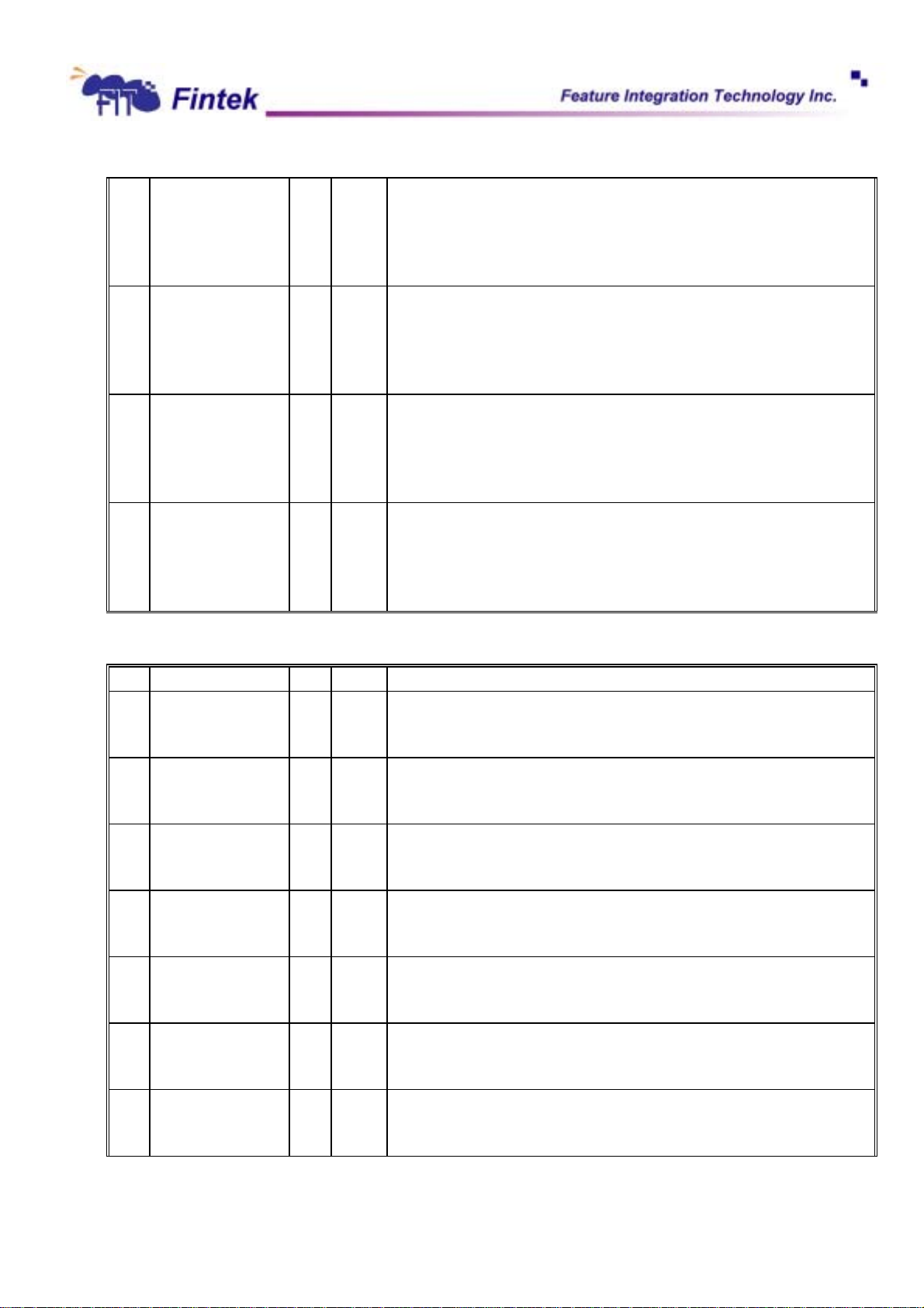
7-6 GP07_PW_SEL R/W 00 GP07 pulse width select:
5-4 GP06_PW_SEL R/W 00 GP06 pulse width select:
3-2 GP05_PW_SEL R/W 00 GP05 pulse width select:
1-0 GP04_PW_SEL R/W 00 GP04 pulse width select:
F71805
00: 500us (default).
01: 1ms.
10: 20ms.
11: 100ms.
00: 500us (default).
01: 1ms.
10: 20ms.
11: 100ms.
00: 500us (default).
01: 1ms.
10: 20ms.
11: 100ms.
00: 500us (default).
01: 1ms.
10: 20ms.
11: 100ms.
7.7.2.8 GP0 Pulse Mode Register Index E6h
Bit Name R/W Default Description
7 GP07_PUL_MODE R/W 0 GP07 pulse mode:
0: output low pulse when in pulse mode.
1: output high pulse when in pulse mode.
6 GP06_PUL_MODE R/W 0 GP06 pulse mode:
0: output low pulse when in pulse mode.
1: output high pulse when in pulse mode.
5 GP05_PUL_MODE R/W 0 GP05 pulse mode:
0: output low pulse when in pulse mode.
1: output high pulse when in pulse mode.
4 GP04_PUL_MODE R/W 0 GP04 pulse mode:
0: output low pulse when in pulse mode.
1: output high pulse when in pulse mode.
3 GP03_PUL_MODE R/W 0 GP03 pulse mode:
0: output low pulse when in pulse mode.
1: output high pulse when in pulse mode.
2 GP02_PUL_MODE R/W 0 GP02 pulse mode:
0: output low pulse when in pulse mode.
1: output high pulse when in pulse mode.
1 GP01_PUL_MODE R/W 0 GP01 pulse mode:
0: output low pulse when in pulse mode.
1: output high pulse when in pulse mode.
79
Dec., 2006
V0.25P
Page 82
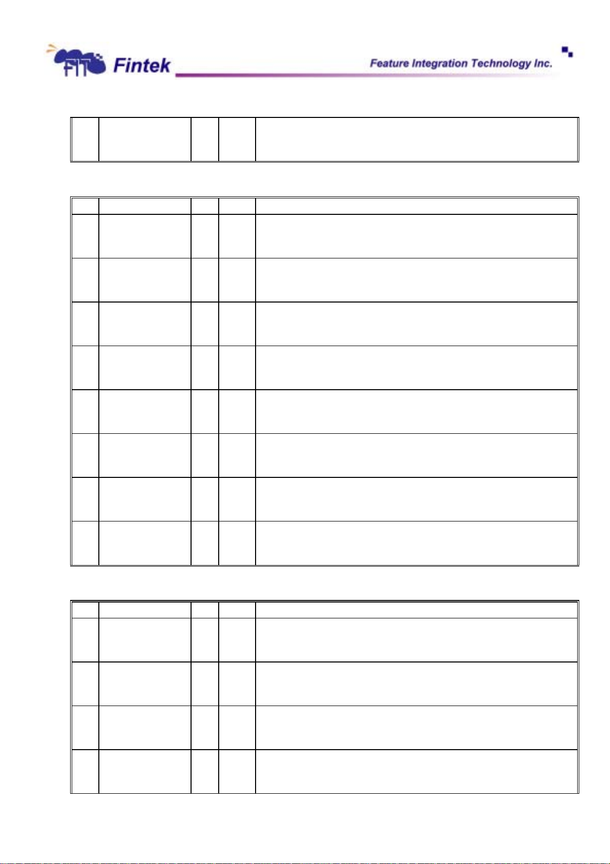
0 GP00_PUL_MODE R/W 0 GP00 pulse mode:
7.7.2.9 GP0 Pad Type Register Index E7h
Bit Name R/W Default Description
7 GP07_DRV_EN R/W 0 GP07 pad type:
6 GP06_DRV_EN R/W 0 GP06 pad type:
5 GP05_DRV_EN R/W 0 GP05 pad type:
4 GP04_DRV_EN R/W 0 GP04 pad type:
3 GP03_DRV_EN R/W 0 GP03 pad type:
2 GP02_DRV_EN R/W 0 GP02 pad type:
1 GP01_DRV_EN R/W 0 GP01 pad type:
0 GP00_DRV_EN R/W 0 GP00 pad type:
F71805
0: output low pulse when in pulse mode.
1: output high pulse when in pulse mode.
0: open drain.
1: push-pull.
0: open drain.
1: push-pull.
0: open drain.
1: push-pull.
0: open drain.
1: push-pull.
0: open drain.
1: push-pull.
0: open drain.
1: push-pull.
0: open drain.
1: push-pull.
0: open drain.
1: push-pull.
7.7.2.10 GP0 IRQ Enable Register Index E8h
Bit Name R/W Default Description
7 GP07_IRQ_EN R/W 0 GP07 interrupt enable:
0: disable interrupt.
1: assert an interrupt when GP07 changed in input mode.
6 GP06_IRQ_EN R/W 0 GP06 interrupt enable:
0: disable interrupt.
1: assert an interrupt when GP06 changed in input mode.
5 GP05_IRQ_EN R/W 0 GP05 interrupt enable:
0: disable interrupt.
1: assert an interrupt when GP05 changed in input mode.
4 GP04_IRQ_EN R/W 0 GP04 interrupt enable:
0: disable interrupt.
1: assert an interrupt when GP04 changed in input mode.
80
Dec., 2006
V0.25P
Page 83
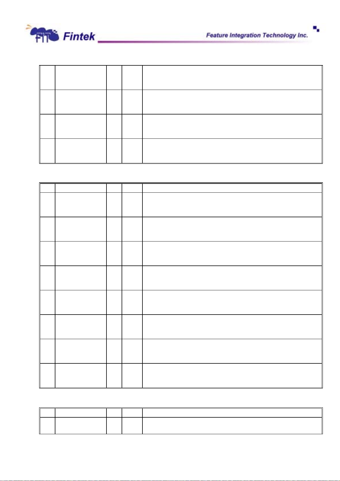
3 GP03_IRQ_EN R/W 0 GP03 interrupt enable:
2 GP02_IRQ_EN R/W 0 GP02 interrupt enable:
1 GP01_IRQ_EN R/W 0 GP01 interrupt enable:
0 GP00_IRQ_EN R/W 0 GP00 interrupt enable:
7.7.2.11 GP0 Edge Detect Register Index E9h
F71805
0: disable interrupt.
1: assert an interrupt when GP03 changed in input mode.
0: disable interrupt.
1: assert an interrupt when GP02 changed in input mode.
0: disable interrupt.
1: assert an interrupt when GP01 changed in input mode.
0: disable interrupt.
1: assert an interrupt when GP00 changed in input mode.
Bit Name R/W Default Description
7 GP07_EDG R/W 0 GP07 edge detect:
0: input data does not change.
1: input data changes. Write 1 to clear.
6 GP06_EDG R/W 0 GP06 edge detect:
0: input data does not change.
1: input data changes. Write 1 to clear.
5 GP05_EDG R/W 0 GP05 edge detect:
0: input data does not change.
1: input data changes. Write 1 to clear.
4 GP04_EDG R/W 0 GP04 edge detect:
0: input data does not change.
1: input data changes. Write 1 to clear.
3 GP03_EDG R/W 0 GP03 edge detect:
0: input data does not change.
1: input data changes. Write 1 to clear.
2 GP02_EDG R/W 0 GP02 edge detect:
0: input data does not change.
1: input data changes. Write 1 to clear.
1 GP01_EDG R/W 0 GP01 edge detect:
0: input data does not change.
1: input data changes. Write 1 to clear.
0 GP00_EDG R/W 0 GP00 edge detect:
0: input data does not change.
1: input data changes. Write 1 to clear.
7.7.2.12 GP1 Output Enable Register Index F0h
Bit Name R/W Default Description
7 GP17_OE R/W 0 0: GP17 is in input mode.
1: GP17 is in output mode.
81
Dec., 2006
V0.25P
Page 84
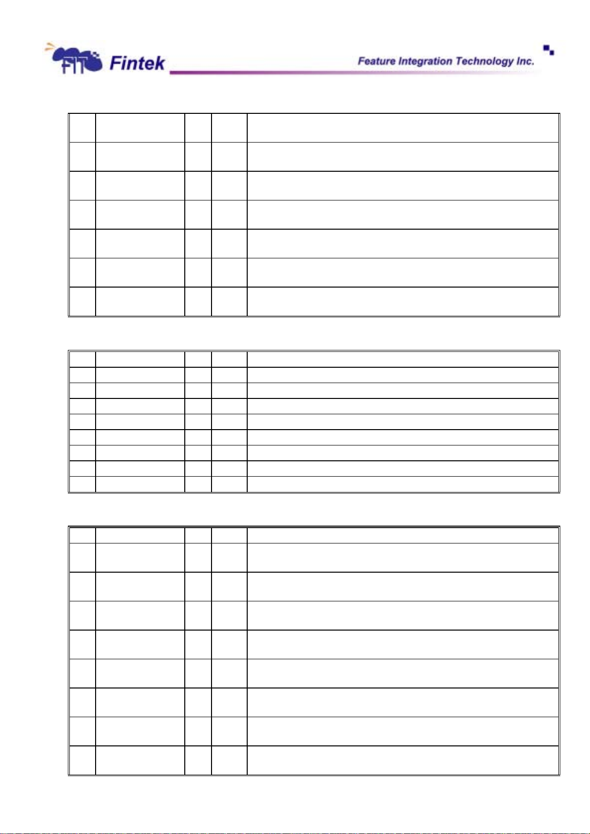
6 GP16_OE R/W 0 0: GP16 is in input mode.
5 GP15_OE R/W 0 0: GP15 is in input mode.
4 GP14_OE R/W 0 0: GP14 is in input mode.
3 GP13_OE R/W 0 0: GP13 is in input mode.
2 GP12_OE R/W 0 0: GP12 is in input mode.
1 GP11_OE R/W 0 0: GP11 is in input mode.
0 GP10_OE R/W 0 0: GP10 is in input mode.
F71805
1: GP16 is in output mode.
1: GP15 is in output mode.
1: GP14 is in output mode.
1: GP13 is in output mode.
1: GP12 is in output mode.
1: GP11 is in output mode.
1: GP10 is in output mode.
7.7.2.13 GP1 Pin Status Register Index F1h
Bit Name R/W Default Description
7 GP17_IN R - The pin status of FA7/GP17.
6 GP16_IN R - The pin status of FA6/GP16.
5 GP15_IN R - The pin status of FA5/GP15.
4 GP14_IN R - The pin status of FA4/GP14.
3 GP13_IN R - The pin status of FA3/GP13.
2 GP12_IN R - The pin status of FA2/GP12.
1 GP11_IN R - The pin status of FA1/GP11.
0 GP10_IN R - The pin status of FA0/GP10.
7.7.2.14 GP2 Output Enable Register Index F3h
Bit Name R/W Default Description
7 GP27_OE R/W 0 0: GP27 is in input mode.
1: GP27 is in output mode.
6 GP26_OE R/W 0 0: GP26 is in input mode.
1: GP26 is in output mode.
5 GP25_OE R/W 0 0: GP25 is in input mode.
1: GP25 is in output mode.
4 GP24_OE R/W 0 0: GP24 is in input mode.
1: GP24 is in output mode.
3 GP23_OE R/W 0 0: GP23 is in input mode.
1: GP23 is in output mode.
2 GP22_OE R/W 0 0: GP22 is in input mode.
1: GP22 is in output mode.
1 GP21_OE R/W 0 0: GP21 is in input mode.
1: GP21 is in output mode.
0 GP20_OE R/W 0 0: GP20 is in input mode.
1: GP20 is in output mode.
82
Dec., 2006
V0.25P
Page 85
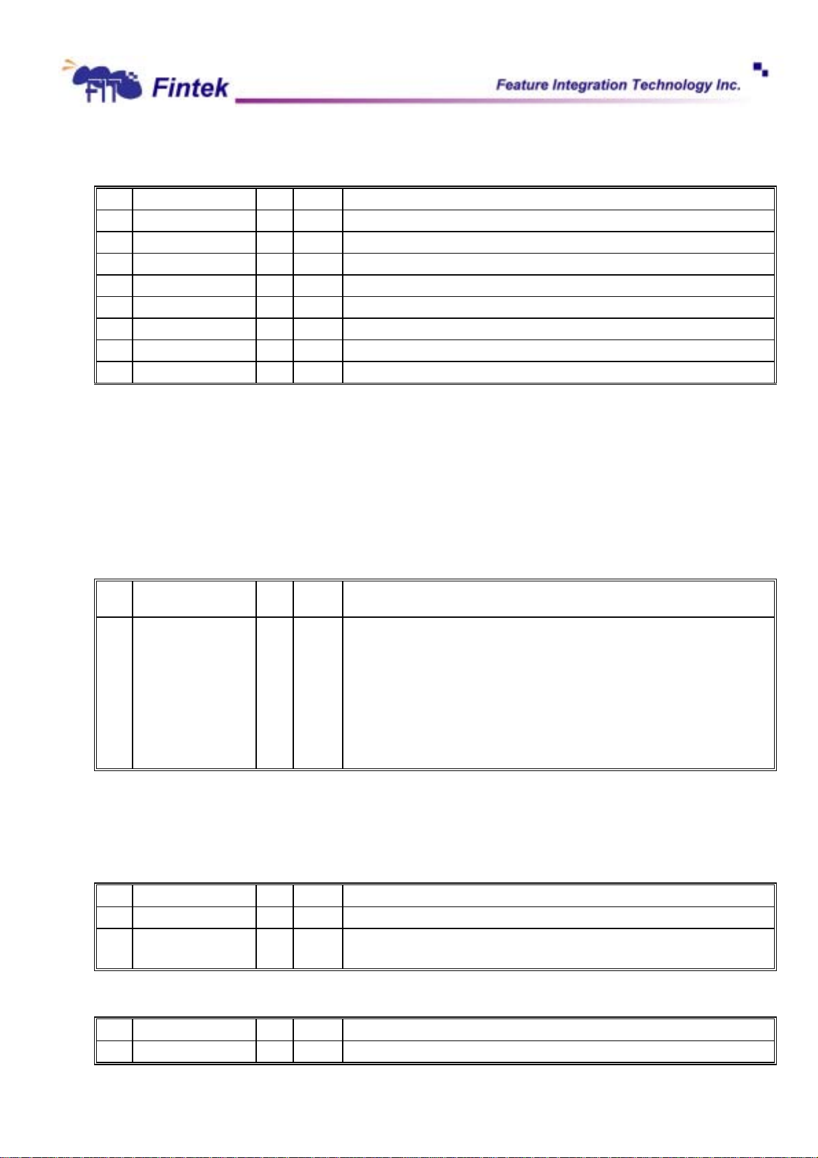
7.7.2.15 GP2 Pin Status Register Index F4h
Bit Name R/W Default Description
7 GP27_IN R - The pin status of FA17/GP27.
6 GP26_IN R - The pin status of FA16/GP26.
5 GP25_IN R - The pin status of FA15/GP25.
4 GP24_IN R - The pin status of FA14/GP24.
3 GP23_IN R - The pin status of FA13/GP23.
2 GP22_IN R - The pin status of FA12/GP22.
1 GP21_IN R - The pin status of FA11/GP21.
0 GP20_IN R - The pin status of FA10/GP20.
F71805
7.8 PME Register
7.8.1 Logic Device Number Register
Logic Device Number Register Index 07h
Bit Name R/W Default Description
7-0 LDN R/W 00h 00h: Select FDC device configuration registers.
01h: Select UART 1 device configuration registers.
02h: Select UART 2 device configuration registers.
03h: Select Parallel Port device configuration registers.
04h: Select Hardware Monitor device configuration registers.
06h: Select GPIO device configuration registers.
0ah: Select PME device configuration registers.
Otherwise: reserved.
7.8.2 PME Configuration Registers
Device Enable Register Index 30h
Bit Name R/W Default Description
7-1 Reserved - - Reserved
0 PME_EN R/W 0 0: disable PME.
1: enable PME.
PME Event Enable Register Index F0h
Bit Name R/W Default Description
7-5 Reserved - - Reserved
83
Dec., 2006
V0.25P
Page 86
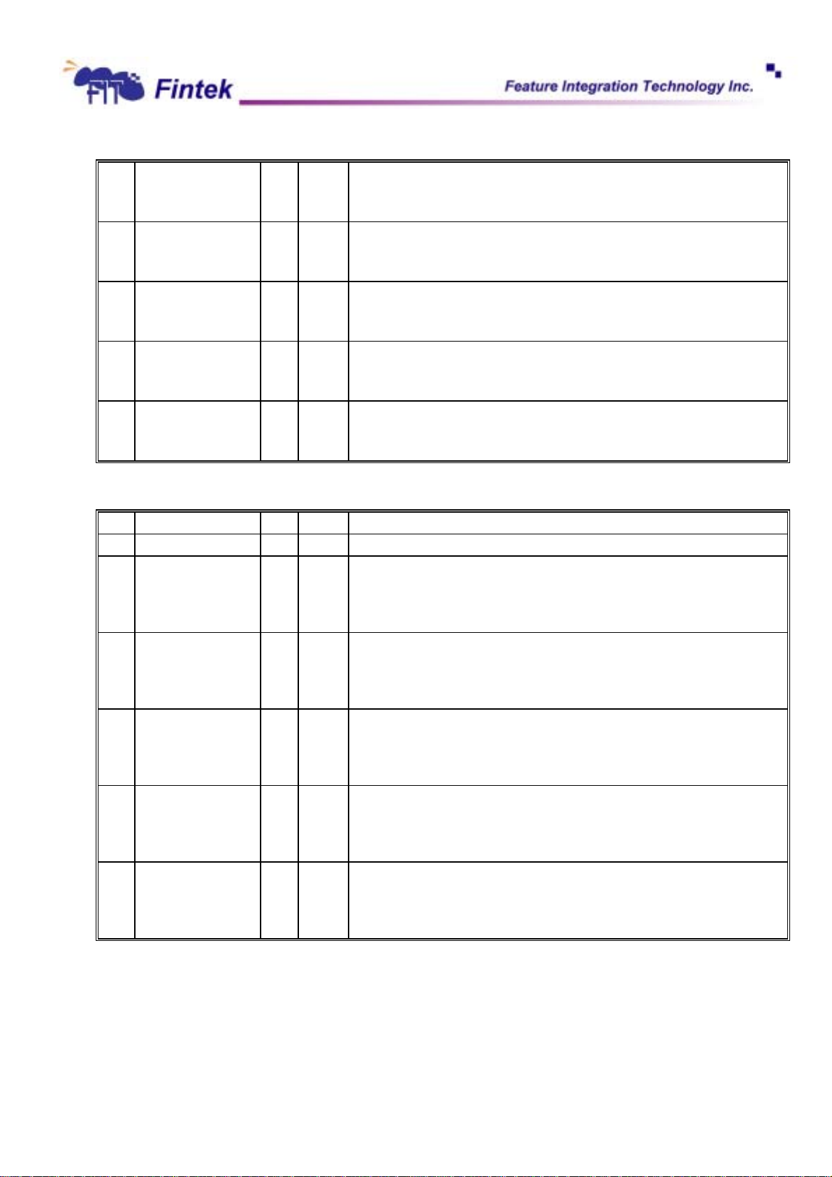
4 HM_PME_EN R/W 0 Hardware monitor PME event enable.
3 PRT_PME_EN R/W 0 Parallel port PME event enable.
2 UR2_PME_EN R/W 0 UART 2 PME event enable.
1 UR1_PME_EN R/W 0 UART 1 PME event enable.
0 FDC_PME_EN R/W 0 FDC PME event enable.
F71805
0: disable hardware monitor PME event.
1: enable hardware monitor PME event.
0: disable parallel port PME event.
1: enable parallel port PME event.
0: disable UART 2 PME event.
1: enable UART 2 PME event.
0: disable UART 1 PME event.
1: enable UART 1 PME event.
0: disable FDC PME event.
1: enable FDC PME event.
PME Event Status Register Index F1h
Bit Name R/W Default Description
7-5 Reserved - - Reserved
4 HM_PME_ST R/W 0 Hardware monitor PME event status.
0: Hardware monitor has no PME event.
1: Hardware monitor has a PME event to assert. Write 1 to clear to be ready for
next PME event.
3 PRT_PME_ST R/W 0 Parallel port PME event status.
0: Parallel port has no PME event.
1: Parallel port has a PME event to assert. Write 1 to clear to be ready for next
PME event.
2 UR2_PME_ST R/W 0 UART 2 PME event status.
0: UART 2 has no PME event.
1: UART 2 has a PME event to assert. Write 1 to clear to be ready for next
PME event.
1 UR1_PME_ST R/W 0 UART 1 PME event status.
0: UART 1 has no PME event.
1: UART 1 has a PME event to assert. Write 1 to clear to be ready for next
PME event.
0 FDC_PME_ST R/W 0 FDC PME event status.
0: FDC has no PME event.
1: FDC has a PME event to assert. Write 1 to clear to be ready for next PME
event.
84
Dec., 2006
V0.25P
Page 87
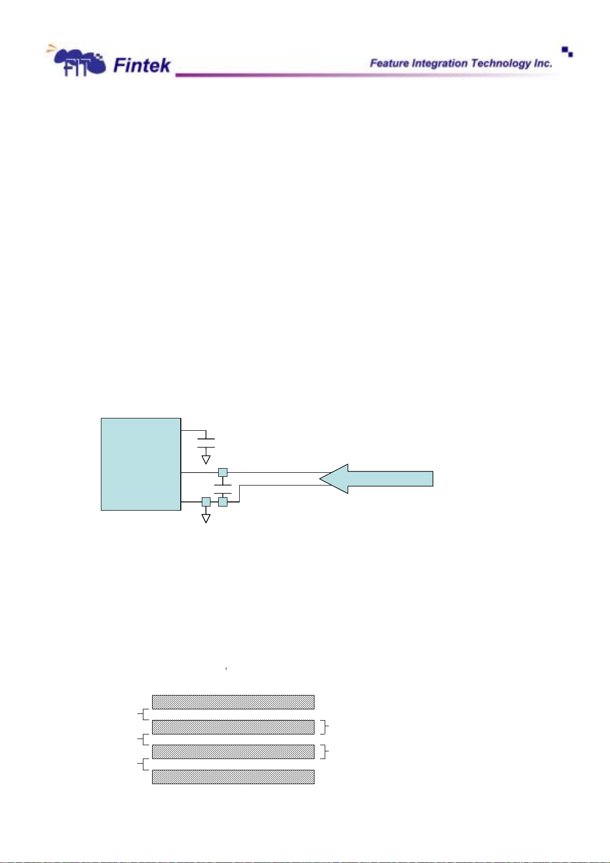
F71805
8. PCB Layout Guide
F71805 adopts Current Mode measure method to do temperature detected. The measure data will not be affected
by different process of CPU due to use current mode technology. This technology measures mini-voltage from the
remote sensor so a good PCB layout must be cared about noise minimizing. The noises often come from circuit trace
which is a track from remote sensor (CPU side) to detect circuit input (F71805 side). The signal on this track will be
inducted mini-noises when it passes through a high electromagnetic area. Those effects will result in the mini-noises
and show in the detected side. It will be reported a wrong data which you want to measure. Please pay attention and
follow up the check list below in order to get an actual and real temperature inside the chip.
1. The D1+/D2+/D3+ and AGND (D-) tracks Must Not pass through/by PWM POWER-MOS. Keep as far as possible
from POWER MOS.
2. Place a 0.1µF bypass capacitor close to the V
across D+, D- and close to the F71805. Near the pin AGND (D-) Must Be placed a through hole into the GND
Plane before connect to the external 2200pF capacitor.
99
99
VCC
3. Place the F71805 as close as practical to the remote sensor diode. In noisy environments, such as a computer
4. Separated route the D1+, D2+ or D3+ with AGND (D-) tracks close together and in parallel after adding external
F71805F
F71805F
main-board, the distance can be 4 to 8 inches. (typ). This length can be increased if the worst noise sources are
avoided. Noise sources generally include clock generators, CRTs, memory buses and PCI/ISA bus etc.
2200pF capacitor. For more reliable, it had better with grounded guard tracks on each side. Provide a ground
plane under the tracks if possible. Do not route D+ & D- lines next to the deflection coil of the CRT. And also don’t
VCC
D1+
D1+
AGND(D-)
AGND(D-)
89
89
86
86
0.1uF
0.1uF
2200pF
2200pF
pin (Pin# 99). Place an external 2200pF input filter capacitors
CC
THERMDA
THERMDA
From thermal diode
THERMDC
THERMDC
From thermal diode
route the trace across fast digital signals which can easily induce bigger error.
GND
10MILS
THERMDA(DXP)
MINIMUM
THERMDC(DXN)
10MILS
GND
85
10MILS
10MILS
Dec., 2006
V0.25P
Page 88
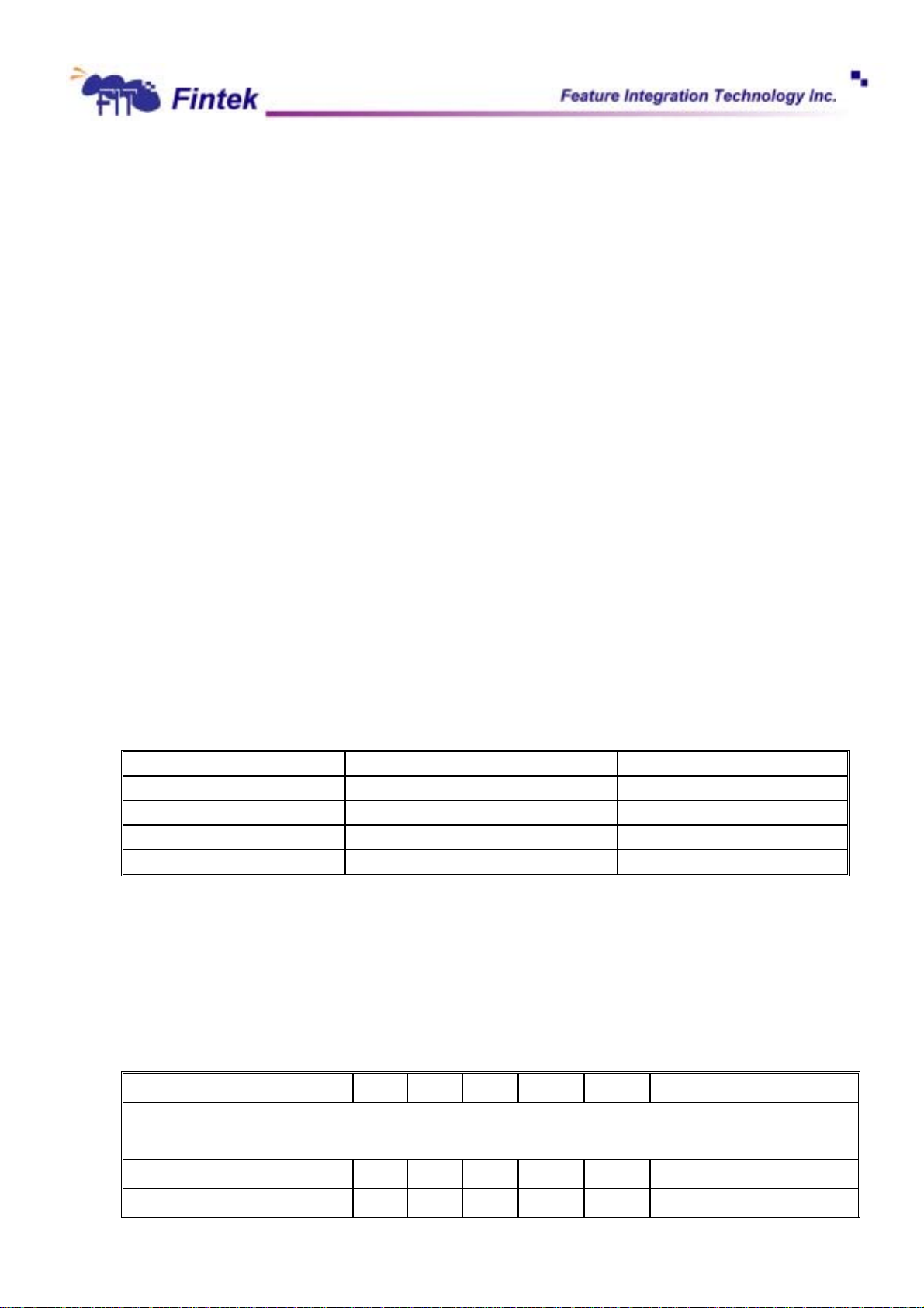
F71805
5. Use wide tracks to minimize inductance and reduce noise pickup. 10 mil track minimum width and spacing is
recommended.
6. Try to minimize the number of component/solder joints, called through hole, which can cause thermocouple effects.
Where through holes are used, make sure that they are in both the D+ and D- path and at the same temperature.
Thermocouple effects should not be a major problem as 1 corresponds to about 200µV. It means that a
copper-solder thermocouple exhibits 3µV/ ,℃ and takes about 200µV of the voltage error at D+ & D- to cause a 1 ℃
measurement error. Adding a few thermocouples causes a negligible error.
7. If the distance to the remote sensor is more than 8 inches, the use of twisted pair cable is recommended. It will
work up to around 6 to 12 feet.
Because the measurement technique uses switched current sources, excessive cable and/or filter capacitance will
affect the measurement accuracy. When using long cables, the filter capacitor should be reduced or removed. Cable
resistance can also induce errors. For example: 1 Ω series resistance introduces about 0.5 error.
℃
℃
9. Electrical characteristic
9.1 Absolute Maximum Ratings
PARAMETER RATING UNIT
Power Supply Voltage -0.5 to 5.5 V
Input Voltage -0.5 to VDD+0.5 V
Operating Temperature 0 to +70 ° C
Storage Temperature -55 to 150 ° C
Note: Exposure to conditions beyond those listed under Absolute Maximum Ratings may adversely
affect the life and reliability of the device
9.2 DC Characteristics
(Ta = 0° C to 70° C, VDD = 3.3V ± 10%, VSS = 0V) (Note)
PARAMETER SYM. MIN. TYP. MAX. UNIT CONDITIONS
I/OD
capability
Input Low Threshold Voltage Vt- V VDD = 3.3 V
Input High Threshold Voltage Vt+ V VDD = 3.3 V
- TTL level bi-directional pin, can select to OD by register, with 16 mA source-sink
16ts
86
Dec., 2006
V0.25P
Page 89
Output Low Current IOL mA VOL = 0.4 V
F71805
Input High Leakage ILIH
Input Low Leakage ILIL
I/OD
- TTL level bi-directional pin, can select to OD by register, with 12 mA source-sink
12ts
µA
µA
VIN = VDD
VIN = 0V
capability
Input Low Threshold Voltage Vt- V VDD = 3.3 V
Input High Threshold Voltage Vt+ V VDD = 3.3 V
Output Low Current IOL mA VOL = 0.4 V
Input High Leakage ILIH
Input Low Leakage ILIL
µA
µA
VIN = VDD
VIN = 0V
9.3 AC Characteristics
Serial Bus Timing
PARAMETER SYMBOL MIN. MAX. UNIT
SCL clock period t
Start condition hold time t
Stop condition setup-up time t
DATA to SCL setup time t
DATA to SCL hold time t
-
uS
SCL
uS
HD;SDA
uS
SU;STO
nS
SU;DAT
nS
HD;DAT
SCL and SDA rise time tR uS
SCL and SDA fall time tF nS
10. Ordering Information
Part Number Package Type Production Flow
F71805F
F71805FG
128-QFP (Normal)
128-QFP (Green Package)
87
Commercial, 0°C to +70°C
Commercial, 0°C to +70°C
Dec., 2006
V0.25P
Page 90
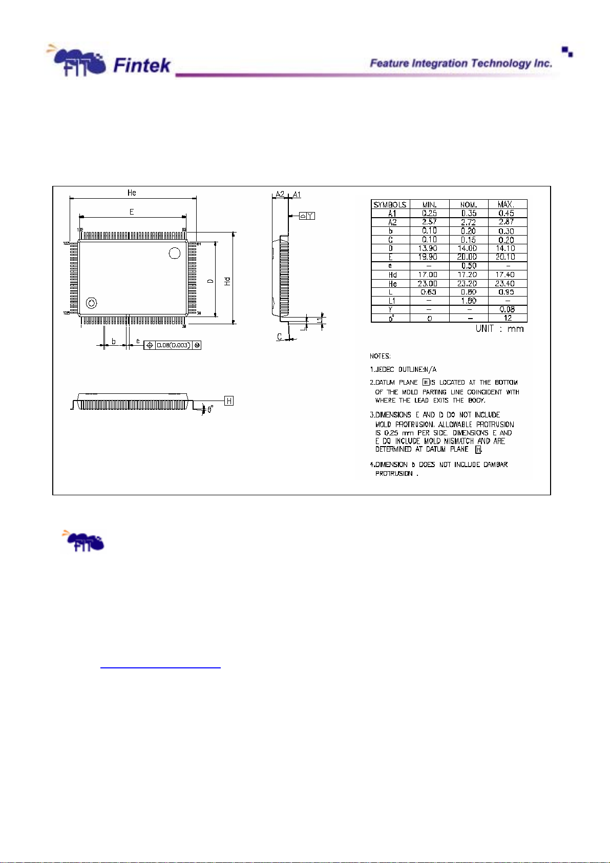
g
11. Package Dimensions
F71805
Feature Integration Technology Inc.
Headquaters
7F, No 31, Shintai Rd.,
Jubei City, Hsinchu 302, Taiwan, R.O.C.
TEL : 886-3-6562727
FAX : 886-3-6560537
www: http://www.fintek.com.tw
Please note that all datasheet and specifications are subject to change without notice. All the trade
Taipei Office
Bldg K4, 7F, No. 700, Chung Cheng Rd.,
Chun
TEL : 886-2-8227-8027
FAX : 886-2-8227-80 37
ho City, Taipei 235, T aiwan, R.O.C.
marks of products and companies mentioned in this datasheet belong to their respective owner
88
Dec., 2006
V0.25P
Page 91
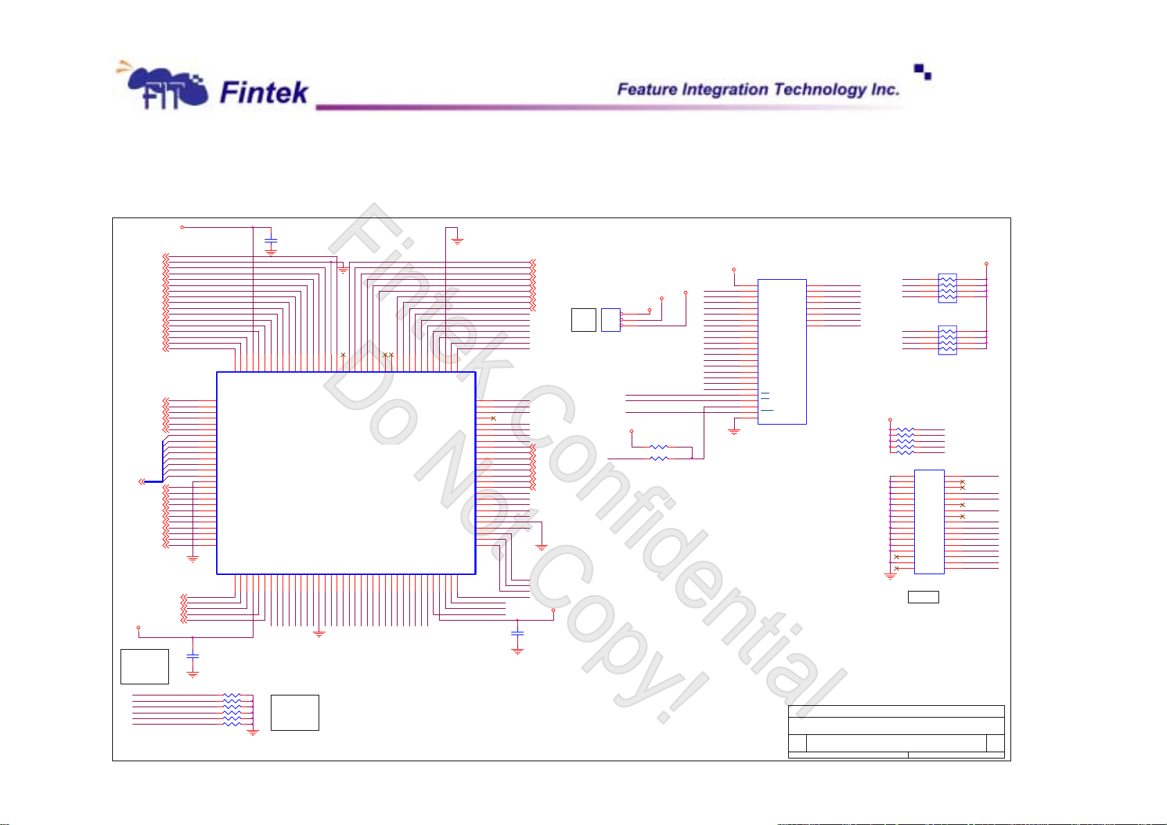
12. F71805 Demo Circuit
VCC3V
No need the Filter
OVT#
DD3+
D2+
D1+
VREF
VIN8
VIN7
VIN6
VIN5
VIN4
VIN3
VIN2
VIN1
SLCT
PE
PD[7..0]
VCC3V
FLASH_SEG1_EN
FLASH_SEG2_EN
FLASH_SEG3_EN
PWM
XBUS
4E
DTR1#
RTS1#
SOUT1
DTR2#
RTS2#
SOUT2
BUSY
ACK#
SLIN#
INIT#
ERR#
AFD#
STB#
DCD1#
RI1#
CTS1#
DTR1#
RTS1#
DSR1#
SOUT1
SIN1
DCD2#
RI2#
CTS2#
DTR2#
RTS2#
DSR2#
SOUT2
SIN2
PD0
PD1
PD2
PD3
PD4
PD5
PD6
PD7
DTR1#
RTS1#
SOUT1
U2
F71805F
DTR2#
RTS2#
SOUT2
+
103
104
105
106
107
108
109
110
111
112
113
114
115
116
117
118
119
120
121
122
123
124
125
126
127
128
C3
0.1U
POWER_ON TRAP PINS
C1
+
0.1U
(GND close to IC)
099
100
101
098
097
096
095
094
093
092
VIN1
VIN2
VIN3
FD0
FD1
FLASH_SEG1_DIS
FLASH_SEG2_DIS
FLASH_SEG3_DIS
LINEAR
RESERVED
2E
091
VIN4
VIN5
VIN6
VIN7
FD3
FD2
FD4
FD5
102
PE
VCC
SLCT
BUSY
ACK#
SLIN#
INIT#
ERR#
AFD#
STB#
PD0
PD1
PD2
PD3
PD4
PD5
PD6
PD7
GND
DCD1#
RI1#
CTS1#
DTR1#
RTS1#
DSR1#
SOUT1
SIN1
DCD2#
RI2#
CTS2#
DTR2#1RTS2#2DSR2#3VCC4SOUT25SIN26FD07FD18FD29FD310FD411FD512FD613FD714GND15FA0/GP1016FA1/GP1117FA2/GP1218FA3/GP1319FA4/GP1420FA5/GP1521FA6/GP1622FA7/GP1723FA824FA925FA10/GP2026FA11/GP2127FA12/GP2228FA13/GP2329FA14/GP2430FA15/GP2531FA16/GP2632FA17/GP2733FRD#34VCC35LDRQ#36SERIRQ37LAD0
R8 4. 7K
R9 4. 7K
R10 4.7K
R11 4.7K
R12 4.7K
R13 4.7K
084
082
085
080
089
088
087
090
086
D1+
D2+
D3+
VIN8
VREF
F71805F
F71805
FA0
FA1
FD6
FD7
079
083
081
N.C4
IRTX
IRRX
OVT#
PME#
GND/ D-
FAN_CTL3
FA2
FA5
FA4
FA3
FA6
FA7
FA8
077
076
078
075
N.C3
N.C2
FAN_CTL2
FAN_CTL1
FA9
FA11
FA10
FA12
071
072
074
073
DSKCHG#
FAN_TAC3
FAN_TAC2
FAN_TAC1
GP03/Voltage_f ault4
GP02/Voltage_f ault3
GP01/Voltage_f ault2
GP00/Voltage_f ault1
FA13
FA15
FA14
FA16
068
067
069
070
WPT#
TRK0#
INDEX#
RDATA#
GP06/VIN7_ID2
GP05/VIN7_ID1
GP04/VIN7_ID0
FA17
066
065
GND
HDSEL#
WGATE#
STEP#
DIR#
WDATA#
N.C1
DRVA#
FA18
MTRA#
DENSEL#
GP07
FWE#
FCS#
LFRAME#
LRESET#
CLKIN
GND
PCICLK
LAD3
LAD2
LAD1
38
64
63
62
61
60
59
58
57
56
55
54
53
52
51
50
49
48
47
46
45
44
43
42
41
40
39
SERIR Q
LDRQ#
FRD#
DSKCHG#
WPT#
INDEX#
TRK0 #
RDATA#
WGATE#
HDSEL#
STEP#
DIR#
WDATA#
DRVA#
FA18
MTRA #
DENSEL#
GP06
GP05
GP04
GP03
GP02
GP01
GP00
FWE#
FCS#
LFRAME#
LRESET#
CLKIN
PCIC LK
LAD3
LAD2
LAD1
LAD0
IRRX
IRTX
PME#
FAN_CTL3
FAN_CTL2
FAN_CTL1
FANIN3
FANIN2
FANIN1
FANCTL
GP06
GP05
GP04
GP03
GP02
GP01
GP00
VCC3V
C2
+
0.1U
3V
ROM
5V
JP1
HEADER 3
1
2
3
VCC_ROM
FA18
R7 0
VCC_ROM
VCC3V
FCS#
FRD#
FWE#
R4 4. 7k
VCC5V
VCC_ROM
U1
32
12
11
10
9
8
7
6
5
27
26
23
25
4
28
29
3
2
30
22
24
1
31
16
VCC
A0
A1
A2
A3
A4
A5
A6
A7
A8
A9
A10
A11
A12
A13
A14
A15
A16
A17
CE
OE
VPP
PGM
GND
FLASH ROM
FA0
FA1
FA2
FA3
FA6 FD7
FA7
FA8
FA9
FA10
FA11
FA12
FA13
FA14
FA15
FA16
FA17
13
O0
14
O1
15
O2
17
O3
18
O4
19
O5
20
O6
21
O7
ISA INTERFACE ROM
Titl e
Feature I ntegration Technology Inc.
Size Document Number Rev
F71805F 0.11
B
Date: Sheet
RN1
FD0
FD1
FD2
FD3
FD4
FD5FA4
FD6FA5
FD0
FD1
FD2
FD3
FD7
FD6
FD5
FD4
VCC5V
R1 1K
R2 1K
R3 1K
R5 1K
R6 1K
J1
1
1
3
3
5
5
7
7
9
9
11
11
13
13
15
15
17
17
19
19
21
21
23
23
25
25
27
27
29
29
31
31
33
33
HEADER 17X2
FLOPPY CONN.
FDC
WPT#
INDEX#
TRK 0#
RDATA#
DSKCHG#
10
12
14
16
18
20
22
24
26
28
30
32
34
4.7K-8P4R
RN2
4.7K-8P4R
2
2
4
4
6
6
8
8
10
12
14
16
18
20
22
24
26
28
30
32
34
14Monday, August 09, 2004
78
56
34
12
78
56
34
12
of
89 Dec., 2006
V0.25P
VCC_ROM
DENSEL#
INDEX#
MTRA#
DRVA#
DIR#
STEP#
WDATA#
WGATE#
TRK0 #
WPT#
RDATA#
HDSEL#
DSKCHG#
Page 92
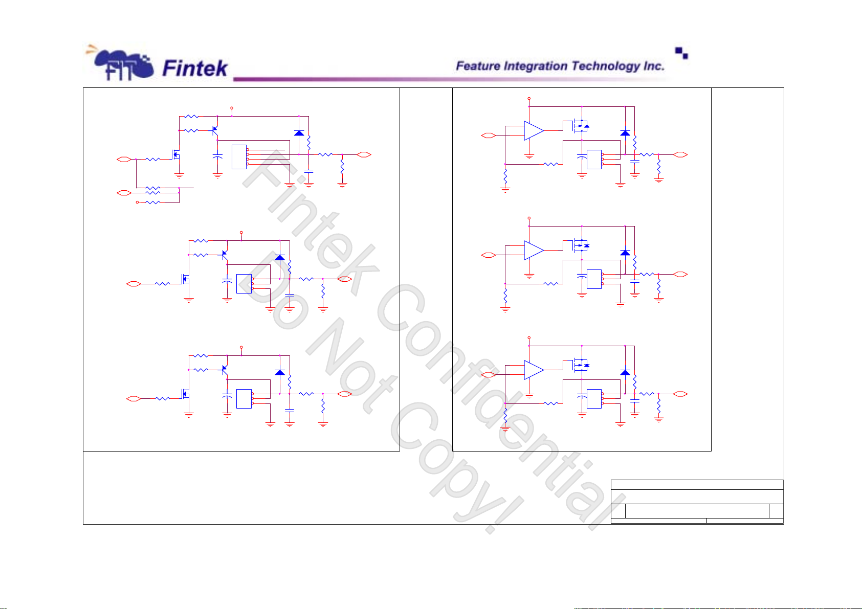
VCC5V
R20 330
R25 0
R26 0
R27 10K
FANCTL1
FANCTL
FANCTL2
1K
C4
10U
1K
Q6
MOSFET N
2N7002
Q2
PNP
4 HEADER
+
C8
10U
+12V
Q5
PNP
+
R14 4.7K
R15
Q3
MOSFET N
2N7002
4FANC TL
PWM FAN 1 SPEED CONTROL
The C10 is reserved for FAN noise dis-bounce.
R28 4.7K
R29
R34 330
4
3
2
1
JP2
+12V
JP5
3
2
1
HEADER 3
1N4148
1N4148
4FANC TL
D4
D1
R31
4.7K
R33 27K
C11
0.1U
R16
4.7K
R18 27K
C7
0.1U
R37
10K
R21
10K
FANIN2
FANIN1
FANCTL1
FANCTL2
12V
NDS0605/ SOT
R24
3.9K
84
U3A
3
+
1
2
-
LM358
R22 10K
Q1
JP3
C5
47u
CON3
DC FAN Control with OP 1
12V
NDS0605/ SOT
84
R38
3.9K
U3B
5
+
7
6
-
LM358
R35 10K
Q4
JP4
C9
47u
CON3
3
2
1
3
2
1
1N4148
1N4148
D2
R17
4.7K
R19 27K
C6
R23
0.1u
10K
D3
R30
4.7K
R32 27K
C10
R36
0.1u
10K
FANIN1
FANIN2
DC FAN Control with OP 2
12V
NDS0605/ SOT
R49
3.9K
84
U4A
3
+
1
2
-
LM358
R47 10K
C13
47u
JP7
CON3
Q7
3
2
1
DC FAN Control with OP 3
1N4148
D6
R42
4.7K
C14
R44 27K
0.1u
R48
10K
FANIN3
FANCTL3
PWM FAN 2 SPEED CONTROL
The C13 is reserved for FAN noise dis-bounce.
R39 4.7K
R40
R45 330
Q9
MOSFET N
2N7002
PWM FAN 3 SPEED CONTROL
The C17 is reserved for FAN noise dis-bounce.
Q8
1K
PNP
C12
+
10U
+12V
JP6
3
2
1
HEADER 3
1N4148
D5
R41
4.7K
R43 27K
C15
0.1U
R46
10K
FANIN3
FANCTL3
FAN CONTROL FOR PWM OR DC
Tit le
Feature I ntegration Technology Inc.
Size Docum ent Num ber R ev
FAN Control 0.11
B
Date: Sheet
of
24Monday, August 09, 2004
90 Dec., 2006
V0.25P
Page 93
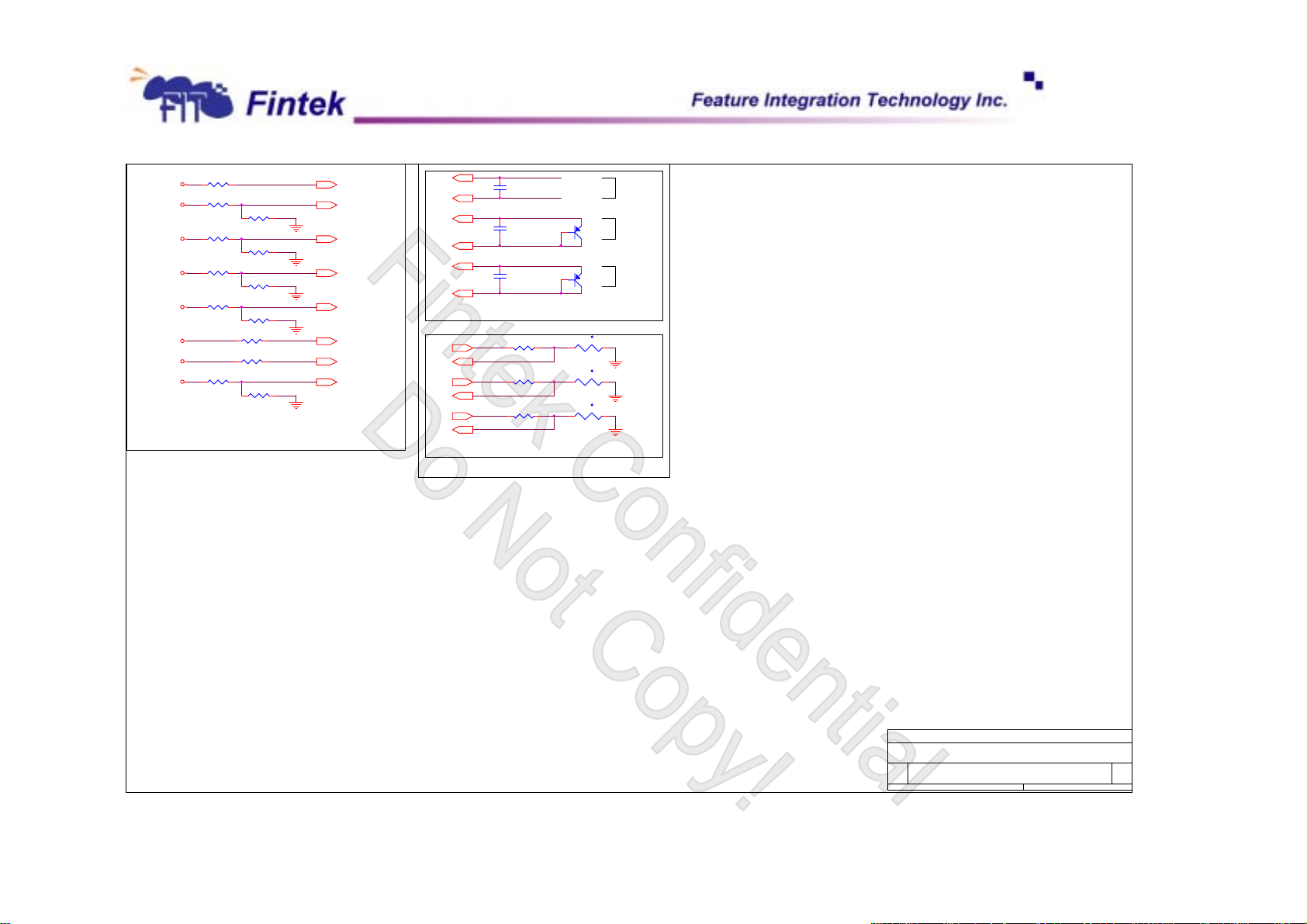
VTT1.2V
VCHIPSET
VCC5V
VCC1.5V
VCORE
The best voltage input level is about 1V.
R50 10K
R51 100K
VRAM
R53 47K
R55 200K
R57 200K
+12V
R62 200K
VSB5V
VOLTAGE SENSING.
R52 100K
R54 100K
R56 47K
R58 20K
R59 10K
R61 10K
R64 47K
VIN1
VIN2
VIN3
VIN4
VIN5
VIN6
VIN7
VIN8
VIN1
VIN2
VIN3
VIN4
VIN5
VIN6
VIN7
VIN8
D1+
D-
D2+
D-
D3+
D-
VREF
D1+
VREF
D2+
VREF
D3+
C16 3300P
D2+
C17 3300P
D3+
C18 3300P
DIODE SENSING CIRCUIT
R60 10K 1%
R63 10K 1%
R65 10K 1%
D+D1+
D-
RT1
THERMISTOR
RT2
THERMISTOR
RT3
THERMISTOR
Q10
PNP
3906
Q11
PNP
3906
10K 1%
T
10K 1%
T
10K 1%
T
from CPU
for
SYSTEM
for
SYSTEM
(for system)
(for system)
(for system)
THERMISTOR SENSING CIRCUIT
Temperature Sensing
Titl e
Feature Integration Technology Inc
Size Document Number Rev
Hardware Monitor 0.1
B
Date: Sheet
of
34Monday, August 09, 2004
91 Dec., 2006
V0.25P
Page 94
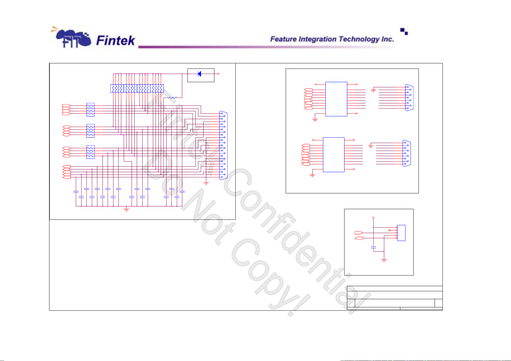
C26
180p
1 2
3 4
5 6
7 8
1 2
3 4
5 6
7 8
1 2
3 4
5 6
7 8
C28
180p
AFD#
INIT#
SLIN#
ERR#
ACK#
BUSY
SLCT
STB#
PD0
PD1
PD2
PD3
PD4
PD5
PD6
PD7
PE
RN7
33-8P4R
RN8
33-8P4R
RN9
33-8P4R
C19
180p
C29
180p
2.7K-8P4R
C20
180p
C30
180p
RN3
C21
180p
RN4
2.7K-8P4R
1 2
3 4
5 6
C22
180p
C31
180p
7 8
RN5
2.7K-8P4R
1 2
3 4
5 6
C32
180p
7 8
2.7K-8P4R
1 2
C23
180p
D7
12
1
14
2
15
3
16
4
17
5
18
6
19
7
20
8
21
9
22
10
23
11
24
12
25
13
(FEMALE)
VCC5V
J2
DB25
VCC5V +12V
RI1#
CTS1#
DSR1#
RTS1#
DTR1#
SIN1
SOUT1
DCD1#
VCC
19
RY1
18
RY2
17
RY3
16
DA1
15
DA2
14
RY4
13
DA3
12
RY5
11
GND
U5
20
UART 1 PORT INTERFACE
U6
20
RI2#
CTS2#
DSR2#
RTS2#
DTR2#
SIN2
SOUT2
DCD2#
VCC5V
VCC
19
RY1
18
RY2
17
RY3
16
DA1
15
DA2
14
RY4
13
DA3
12
RY5
11
GND
UART 2 PORT INTERFACE
+12V
RA1
RA2
RA3
DY1
DY2
RA4
DY3
RA9
-12V
+12V
RA1
RA2
RA3
DY1
DY2
RA4
DY3
RA9
-12V
1
2
3
4
5
6
7
8
9
10
1
RIN1 RIN1
2
CTSN1
3
4
RTSN1
5
DTRN1
6
SINN1
7
SOUTN1
8
DCDN1
9
10
-12V
+12V
RIN2
CTSN2
DSRN2
RTSN2
DTRN2
SINN2
SOUTN2
DCDN2
-12V
GND
DTRN1
CTSN1DSRN1
SOUTN1
RTSN1
SINN1
DSRN1
DCDN1
GND
RIN2
DTRN2
CTSN2
SOUTN2
RTSN2
SINN2
DSRN2
DCDN2
5
9
4
8
3
7
2
6
1
UART DB9
P2
5
9
4
8
3
7
2
6
1
UART DB9
P1
1N5819
C25
180p
C35
180p
C27
180p
FOR LEKAGE TO POWER
RN6
1 2
3 4
5 6
C33
180p
7 8
5 6
7 8
C24
180p
R66 2.7K
C34
180p
3 4
PARALLEL PORT INTERFACE
VCC5V/3V
JP8
1
IRTX
IRRX
C36
0.1U
2
3
4
5
HEADER 5
IR INTERFACE
Titl e
Feature Integration Technology Inc.
Size Document Number Rev
Printer &UART 0.1
B
Date: Sheet
of
44Monday , August 09, 2004
92 Dec., 2006
V0.25P
 Loading...