Fibocom NL668-AM-01, NL668-AM-00 User Manual

FIBOCOM NL668-AM Hardware
User Manual
Version: V1.0.1
Date: 2018-11-13

Applicability type
No. |
Product model |
Description |
1 |
NL668-AM-00 |
MCP is 4+2, and supports MAIN_ANT, DIV_ANT, GNSS_ANT |
2 |
NL668-AM-01 |
Based on NL668-AM-00 delete Band 71 |
Reproduction forbidden without Fibocom Wireless Inc. written authorization - All Rights Reserved.
FIBOCOM NL668-AM Hardware User Manual |
Page 2 of 62 |

Copyright
Copyright ©2018 Fibocom Wireless Inc. All rights reserved.
Without the prior written permission of the copyright holder, any company or individual is prohibited to excerpt, copy any part of or the entire document, or transmit the document in any form.
Attention
The document is subject to update from time to time owing to the product version upgrade or other reasons. Unless otherwise specified, the document only serves as the user guide. All the statements, information and suggestions contained in the document do not constitute any explicit or implicit guarantee.
Trademark
The trademark is registered and owned by Fibocom Wireless Inc.
Versions
Version |
Author |
Assessor |
Approver |
Update |
Description |
|
Date |
||||||
|
|
|
|
|
||
V1.0.0 |
Gaoying |
Chenguojiang |
Tumin |
2018-10-26 |
Initial version |
|
V1.0.1 |
Gaoying |
Chenguojiang |
Tumin |
2018-11-13 |
Add Band 17 |
Reproduction forbidden without Fibocom Wireless Inc. written authorization - All Rights Reserved.
FIBOCOM NL668-AM Hardware User Manual |
Page 3 of 62 |

Contents
1 |
Foreword |
....................................................................................................................... |
9 |
|
|
1.1 |
Introduction................................................................................................................... |
9 |
|
|
1.2 |
Safety ..........................................................................................................Instruction |
9 |
|
|
1.3 |
Reference ..................................................................................................Standards |
10 |
|
|
1.4 |
Related ......................................................................................................Document |
11 |
|
|
1.5 |
Federal .....................................Communication Commission Interference Statement |
11 |
|
2 |
Product Overview....................................................................................................... |
13 |
||
|
2.1 |
Product ...................................................................................................Introduction |
13 |
|
|
2.2 |
Product ................................................................................................Specifications |
13 |
|
|
2.3 |
Hardware .....................................................................................................Diagram |
14 |
|
3 |
Application ..................................................................................................Interface |
16 |
||
|
3.1 |
LCC .............................................................................................................Interface |
16 |
|
|
|
3.1.1 ............................................................................................................... |
Pin distribution |
16 |
|
|
3.1.2 .................................................................................................................. |
Pin definition |
17 |
|
3.2 |
Power .............................................................................................................Supply |
22 |
|
|
|
3.2.1 ................................................................................................................. |
Power supply |
23 |
|
|
3.2.2 ................................................................................................................... |
1.8V Output |
24 |
|
|
3.2.3 ....................................................................................................... |
Power consumption |
24 |
|
3.3 |
Control .............................................................................................................Signal |
25 |
|
|
|
3.3.1 ........................................................................................................... |
Module power on |
26 |
|
|
3.3.2 ........................................................................................................... |
Module power off |
27 |
|
|
3.3.3 ................................................................................................................. |
Module reset |
28 |
|
3.4 |
USB .............................................................................................................Interface |
30 |
|
|
|
3.4.1 ................................................................................................ |
USB interface definition |
30 |
|
3.5 |
USIM ...........................................................................................................Interface |
31 |
|
|
|
3.5.1 ........................................................................................................................ |
USIM pin |
31 |
|
|
3.5.2 .................................................................................................... |
USIM interface circuit |
31 |
|
|
3.5.3 ............................................................................................................... |
USIM hot plug |
33 |
|
|
3.5.4 ........................................................................................... |
USIM design requirements |
34 |
|
3.6 |
UART ...........................................................................................................Interface |
34 |
|
|
|
3.6.1 .............................................................................................. |
UART interface definition |
34 |
|
|
3.6.2 ................................................................................................... |
UART port application |
35 |
|
3.7 |
Status ...........................................................................................................Indicator |
36 |
|
Reproduction forbidden without Fibocom Wireless Inc. written authorization - All Rights Reserved.
FIBOCOM NL668-AM Hardware User Manual |
Page 4 of 62 |

|
3.7.1 |
NET_MODE Signal ....................................................................................................... |
36 |
|
|
3.8 |
Low Power Mode........................................................................................................ |
37 |
|
|
3.8.1 |
Flight mode.................................................................................................................... |
37 |
|
|
3.8.2 |
Sleep Mode ................................................................................................................... |
38 |
|
|
3.9 |
Digital audio interface PCM ........................................................................................ |
40 |
|
|
3.9.1 |
Support model............................................................................................................... |
40 |
|
|
3.9.2 |
PCM interface definition................................................................................................ |
40 |
|
|
3.9.3 |
PCM interface description............................................................................................. |
40 |
|
|
3.9.4 |
PCM signal description ................................................................................................. |
41 |
|
|
3.10 |
ADC function .............................................................................................................. |
42 |
|
4 |
RF Interface................................................................................................................. |
43 |
||
|
4.1 |
NL668-AM Operating Frequency ................................................................................ |
43 |
|
|
4.2 |
RF Output Power of NL668-AM.................................................................................. |
43 |
|
|
4.3 |
RF Receiving Sensitivity of NL668-AM ....................................................................... |
44 |
|
|
4.4 |
GNSS Receiver .......................................................................................................... |
44 |
|
|
4.4.1 |
Basic description ........................................................................................................... |
44 |
|
|
4.5 |
RF PCB Design .......................................................................................................... |
45 |
|
|
4.5.1 |
Antenna RF connector .................................................................................................. |
45 |
|
|
4.6 |
Antenna Design.......................................................................................................... |
46 |
|
5 |
Electrical Characteristics .......................................................................................... |
49 |
||
|
5.1 |
Limiting voltage range................................................................................................. |
49 |
|
|
5.2 |
Environment temperature range ................................................................................. |
49 |
|
|
5.3 |
Electrical characteristics of the interface in operating status ....................................... |
49 |
|
|
5.4 |
Environmental reliability requirements ........................................................................ |
50 |
|
|
5.5 |
ESD characteristics .................................................................................................... |
51 |
|
6 |
Structure Specification .............................................................................................. |
52 |
||
|
6.1 |
Product Appearance ................................................................................................... |
52 |
|
|
6.2 |
Dimension of Structure ............................................................................................... |
53 |
|
|
6.3 |
SMT Patch.................................................................................................................. |
53 |
|
Appendix A Terms and Acronyms................................................................................... |
54 |
|||
Appendix B ADP & MiniPCIe RF ports trace………………………………………………... 57
Reproduction forbidden without Fibocom Wireless Inc. written authorization - All Rights Reserved.
FIBOCOM NL668-AM Hardware User Manual |
Page 5 of 62 |

Figure |
|
Figure 2-1 Hardware Diagram ............................................................................................................ |
15 |
Figure 3-1 Pin Distribution Diagram(TOP plan perspective diagram)................................................ |
16 |
Figure 3-2 Power Design .................................................................................................................... |
23 |
Figure 3-3 Power Limit........................................................................................................................ |
24 |
Figure 3-4 OC/OD Drive Power on Reference Circuit........................................................................ |
26 |
Figure 3-5 Button Power on Reference Circuit................................................................................... |
26 |
Figure 3-6 Power on Timing Control Diagram .................................................................................... |
27 |
Figure 3-7 Power off Timing Control Diagram .................................................................................... |
28 |
Figure 3-8 RESET_N OC/OD Drive Reference Circuit ...................................................................... |
29 |
Figure 3-9 RESET_N Button Reference Circuit ................................................................................. |
29 |
Figure 3-10 Reset Control Timing....................................................................................................... |
29 |
Figure 3-11 SIM Card Slot Diagram SIM016-8P-220P....................................................................... |
32 |
Figure 3-12 USIM/SIM Interface with Detection Signal Reference Design........................................ |
32 |
Figure 3-13 USIM/SIM Interface without Detection Signal Reference Design Diagram.................... |
33 |
Figure 3-14 UART Level Translate Reference Circuit 1..................................................................... |
35 |
Figure 3-15 UART Level Translate Reference Circuit 2..................................................................... |
36 |
Figure 3-16 NET_MODE Reference Design Diagram........................................................................ |
37 |
Figure 3-17 PCM_SYNC Timing......................................................................................................... |
41 |
Figure 3-18 PCM_CODEC to NL668-AM Timing ............................................................................... |
41 |
Figure 3-19 NL668-AM to PCM_CODEC Timing ............................................................................... |
41 |
Figure 3-20 CODEC Timing Parameters ............................................................................................ |
42 |
Figure 4-1RF Reference Circuit Design ............................................................................................. |
45 |
Figure 4-2 GNSS RF Reference Circuit ............................................................................................. |
46 |
Figure 6-1Module Product Appearance (Top) .................................................................................... |
52 |
Figure 6-2 Module Product Appearance (Bottom).............................................................................. |
52 |
Figure 6-3 Dimension of Structure (Unit: mm).................................................................................... |
53 |
Reproduction forbidden without Fibocom Wireless Inc. written authorization - All Rights Reserved.
FIBOCOM NL668-AM Hardware User Manual |
Page 6 of 62 |

Table |
|
Table 2-1 Product Specifications......................................................................................................... |
14 |
Table 3-1 Pin Definitions ..................................................................................................................... |
22 |
Table 3-2 Power Interfaces ................................................................................................................. |
22 |
Table 3-3 Power Filter Capacitor Design ............................................................................................ |
23 |
Table 3-4 VDD_EXT Logic Level ........................................................................................................ |
24 |
Table 3-5 Power Consumption............................................................................................................ |
25 |
Table 3-6 Control Signal...................................................................................................................... |
26 |
Table 3-7 Power Off Modes ................................................................................................................ |
27 |
Table 3-8 Module Reset...................................................................................................................... |
28 |
Table 3-9 USB Interface Definition ..................................................................................................... |
30 |
Table 3-10 SIM Card Pin..................................................................................................................... |
31 |
Table 3-11SIM Card Hot Plug Function Configured AT Commands................................................... |
33 |
Table 3-12 USIM_PRESENCE Effective Level Switched AT command............................................. |
34 |
Table 3-13 Main Serial Port Pin .......................................................................................................... |
35 |
Table 3-14 Debug Serial Port Pin ....................................................................................................... |
35 |
Table 3-15 Network Indication pins..................................................................................................... |
36 |
Table 3-16 Network Indicator Status Description................................................................................ |
37 |
Table 3-17 W_DISABLE# Pin Description.......................................................................................... |
37 |
Table 3-18 Module enter Fly Mode ..................................................................................................... |
37 |
Table 3-19 Support model................................................................................................................... |
40 |
Table 3-20 PCM Interface Definition................................................................................................... |
40 |
Table 3-21 PCM Interface Description................................................................................................ |
40 |
Table 3-22 ADC Interface.................................................................................................................... |
42 |
Table 4-1Operating Frequency ........................................................................................................... |
43 |
Table 4-2 RF Output Power ................................................................................................................ |
43 |
Table 4-3 RF Receiving Sensitivity ..................................................................................................... |
44 |
Table 4-4 GNSS Receiver................................................................................................................... |
45 |
Table 4-5 Main Antenna Requirement ................................................................................................ |
48 |
Table 5-1 Voltage Range..................................................................................................................... |
49 |
Table 5-2Environment Temperature Range........................................................................................ |
49 |
Table 5-3 Electrical Characteristics of the Interface in Operating Status ........................................... |
50 |
Table 5-4 Environmental Reliability Requirements............................................................................. |
50 |
Table 5-5 ESD Allowable Discharge Range ....................................................................................... |
51 |
Reproduction forbidden without Fibocom Wireless Inc. written authorization - All Rights Reserved.
FIBOCOM NL668-AM Hardware User Manual |
Page 7 of 62 |

Table A-0-1 Terms and Acronyms....................................................................................................... |
56 |
Reproduction forbidden without Fibocom Wireless Inc. written authorization - All Rights Reserved.
FIBOCOM NL668-AM Hardware User Manual |
Page 8 of 62 |

1 Foreword
1.1 Introduction
This document describes the electrical characteristics, RF performance, structure size, application environment, etc. of NL668-AM module. With the assistance of the document and other instructions, the developers can quickly understand the hardware functions of the NL668-AM module and develop products.
1.2 Safety Instruction
By following the safety guidelines below, you can ensure your personal safety and help protect the product and work environment from potential damage. Product manufacturers need to communicate the following safety instructions to end users. In case of failure to comply with these safety rules, Fibocom will not be responsible for the consequences caused by the user’s misuse.
Road safety first! When you drive, do not use the handheld devices even if it has a hand-free feature. Please stop and call.
Please turn off the mobile device before boarding. The wireless feature of the mobile device is not allowed on the aircraft to prevent interference with the aircraft communication system. Ignoring this note may result in flight safety issue or even breaking the law.
When in a hospital or health care facility, please be aware of restrictions on the use of mobile devices. Radio frequency interference may cause medical equipment to
malfunction, so it may be necessary to turn off the mobile device.
The mobile device does not guarantee that an effective connection can be made under any circumstances, for example, when there is no prepayment for the mobile device or the SIM is invalid. When you encounter the above situation in an emergency, remember to use an emergency call, while keeping your device turned on and in areas where signal is strong.
Reproduction forbidden without Fibocom Wireless Inc. written authorization - All Rights Reserved.
FIBOCOM NL668-AM Hardware User Manual |
Page 9 of 62 |

Your mobile device receives and transmits RF signals when it is powered on. Radio interference occurs when it is near televisions, radios, computers, or other electronic devices.
Keep the mobile device away from flammable gases. Turn off the mobile device when near gas stations, oil depots, chemical plants or explosive workplaces. There is a safety hazard in operating electronic equipment in any potentially explosive environment.
1.3 Reference Standards
This design of the product complies with the following standards:
3GPP TS 51.010-1 V10.5.0: Mobile Station (MS) conformance specification; Part 1: Conformance specification
3GPP TS 34.121-1 V10.8.0: User Equipment (UE) conformance specification; Radio transmission and reception (FDD); Part 1: Conformance specification
3GPP TS 34.122 V10.1.0: Technical Specification Group Radio Access Network; Radio transmission and reception (TDD)
3GPP TS 36.521-1 V10.6.0: User Equipment (UE) conformance specification; Radio transmission and reception; Part 1: Conformance testing
3GPP TS 21.111 V10.0.0: USIM and IC card requirements
3GPP TS 51.011 V4.15.0: Specification of the Subscriber Identity Module -Mobile Equipment (SIM-ME) interface
3GPP TS 31.102 V10.11.0: Characteristics of the Universal Subscriber Identity Module (USIM) application
3GPP TS 31.11 V10.16.0: Universal Subscriber Identity Module (USIM) Application Toolkit(USAT)
3GPP TS 36.124 V10.3.0: Electro Magnetic Compatibility (EMC) requirements for mobile terminals and ancillary equipment
3GPP TS 27.007 V10.0.8: AT command set for User Equipment (UE)
3GPP TS 27.005 V10.0.1: Use of Data Terminal Equipment - Data Circuit terminating Equipment
(DTE - DCE) interface for Short Message Service (SMS) and Cell Broadcast Service (CBS)
Reproduction forbidden without Fibocom Wireless Inc. written authorization - All Rights Reserved.
FIBOCOM NL668-AM Hardware User Manual |
Page 10 of 62 |

1.4Related Document
FIBOCOM_RF Antenna Application Design Instruction
FIBOCOM_ADP-NL668 Evaluation board instruction
FIBOCOM_NL668 AT Command Manual
FIBOCOM_EVK-GT8230-NL User Manual
FIBOCOM_ NL668 LCC SMT Application Design Instruction
1.5Federal Communication Commission Interference Statement
FCC Regulations:
This device complies with part 15 of the FCC Rules. Operation is subject to the following two conditions:
(1) This device may not cause harmful interference, and (2) This device must accept any interference received, including interference that may cause undesired operation.
This device has been tested and found to comply with the limits for a Class B digital device , pursuant to Part 15 of the FCC Rules. These limits are designed to provide reasonable protection against harmful interference in a residential installation. This equipment generates, uses and can radiated radio frequency energy and, if not installed and used in accordance with the instructions, may cause harmful interference to radio communications. However, there is no guarantee that interference will not occur in a particular installation If this equipment does cause harmful interference to radio or television reception, which can be determined by turning the equipment off and on, the user is encouraged to try to correct the interference by one or more of the following measures:
-Reorient or relocate the receiving antenna.
-Increase the separation between the equipment and receiver.
-Connect the equipment into an outlet on a circuit different from that to which the receiver is connected. -Consult the dealer or an experienced radio/TV technician for help.
Caution: Changes or modifications not expressly approved by the party responsible for compliance could void the user‘s authority to operate the equipment.
RF Exposure Information:
This device complies with FCC radiation exposure limits set forth for an uncontrolled environment. In order to avoid the possibility of exceeding the FCC radio frequency exposure limits, human proximity to the antenna shall not be less than 20cm (8 inches) during normal operation.
Reproduction forbidden without Fibocom Wireless Inc. written authorization - All Rights Reserved.
FIBOCOM NL668-AM Hardware User Manual |
Page 11 of 62 |

IMPORTANT NOTE :
This module is intended for OEM integrator. The OEM integrator is still responsible for the FCC compliance requirement of the end product, which integrates this module. 20cm minimum distance has to be able to be maintained between the antenna and the users for the host this module is integrated into. Under such configuration, the FCC radiation exposure limits set forth for an population/uncontrolled environment can be satisfied.
Any changes or modifications not expressly approved by the manufacturer could void the user's authority to operate this equipment.
USERS MANUAL OF THE END PRODUCT :
In the user manual of the end product, the end user has to be informed to keep at least 20cm separation with the antenna while this end product is installed and operated. The end user has to be informed that the FCC radio-frequency exposure guidelines for an uncontrolled environment can be satisfied. The end user has to also be informed that any changes or modifications not expressly approved by the manufacturer could void the user's authority to operate this equipment. If the size of the end product is smaller than 8x10cm, then additional FCC part 15.19 statement is required to be available in the users manual: This device complies with Part 15 of FCC rules. Operation is subject to the following two conditions: (1) this device may not cause harmful interference and (2) this device must accept any interference received, including interference that may cause undesired operation.
LABEL OF THE END PRODUCT :
The final end product must be labeled in a visible area with the following " Contains Transmitter Module FCC ID: ZMONL668AM01". If the size of the end product is larger than 8x10cm, then the following FCC part 15.19 statement has to also be available on the label: This device complies with Part 15 of FCC rules. Operation is subject to the following two conditions: (1) this device may not cause harmful interference and (2) this device must accept any interference received, including interference that may cause undesired operation.
Reproduction forbidden without Fibocom Wireless Inc. written authorization - All Rights Reserved.
FIBOCOM NL668-AM Hardware User Manual |
Page 12 of 62 |

2 Product Overview
2.1 Product Introduction
The NL668-AM wireless module is a wideband wireless terminal product applicable to various network formats and multi-bands including FDD-LTE/UMTS.
2.2 Product Specifications
Specification
 Operating
frequency
Data  transmission
 Power
Power
 Temperature
 Power
Power
 consumption
 Physical
 characteristics
Interface
LTE FDD: Band 2,4,5,12,13,17,66,71
 WCDMA: Band 2,4,5
LTE FDD: Band 2,4,5,12,13,17,66
 WCDMA: Band 2,4,5
  150Mbps DL/50Mbps UL(Cat 4); LTE Downlink MIMO 2x2, 4x2
 WCDMA:384 kbps DL/384 kbps UL
DC-HSDPA+:42Mbps (Cat 24)/HSUPA:5.76Mbps (Cat 6)
 3.3V 4.3V (3.8V recommended)
Normal: -30°C +75°C
 Extended: -40°C +85°C
Storage: -40°C +85°C
 Base current: <1.5mA
Sleep mode: ≤3mA
 Idle mode: <20mA
  Package: LCC 144PIN
Size: 32.0×29.0×2.4 mm Weight: About 5.5g
Antenna |
Antenna: Main x 1, GNSS x 1, DIV x 1 |
Functional |
USIM 3.0V/1.8V |
Reproduction forbidden without Fibocom Wireless Inc. written authorization - All Rights Reserved.
FIBOCOM NL668-AM Hardware User Manual |
Page 13 of 62 |
Interface |
USB 2.0 x 1 |
|
UART, PCM, I2C, SGMII, SDIO, GPIO, SPI |
|
System Indicator |
|
ADC |
Software |
|
Protocol Stack AT Command Firmware update
Voice service
SMS
MMS service
Note:
Embedded TCP/IP and UDP/IP protocol stack
3GPP TS 27.007 and 27.005, and proprietary FIBOCOM AT USB(UART does not support DOWNLOAD)
VoLTE, HR, FR, EFR, AMR, DTMF, Caller ID, Call Transfer, Call Hold, Call Waiting and Multi-Talk, etc.
point-to-point MO, MT; cell broadcast; support Text and PDU modes Need AP to realize MMS protocol
Table 2-1 Product Specifications
When the temperature is beyond the normal operating temperature range (-30 °C to + 75 °C), the RF performance of the module may slightly exceed the 3GPP specifications.
2.3 Hardware Diagram
Figure 2-2 hardware diagram shows the main hardware features of the NL668-AM module, including baseband and RF features.
Baseband includes:
UMTS/ LTE FDD controller
PMIC
MCP
UART USB SIM PCM I2C SPI SGMII SDIO ADC
RF includes:
RF Transceiver
RF PA
RF filter
Antenna
Reproduction forbidden without Fibocom Wireless Inc. written authorization - All Rights Reserved.
FIBOCOM NL668-AM Hardware User Manual |
Page 14 of 62 |

Figure 2-1 Hardware Diagram
Reproduction forbidden without Fibocom Wireless Inc. written authorization - All Rights Reserved.
FIBOCOM NL668-AM Hardware User Manual |
Page 15 of 62 |
3 Application Interface
3.1 LCC Interface
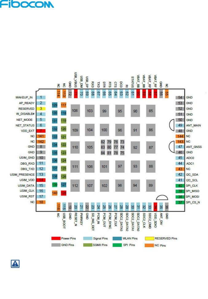
NL668-AM module adopts LCC packaging, with a total of 144 pins.
3.1.1 Pin distribution
Figure 3-1 Pin Distribution Diagram(TOP plan perspective diagram)
Note:
“73 ~ 112” is the thermal pin, and the module is grounded internally. It is recommended that the
heat sink pad is reserved for PCB packaging and welded.
Reproduction forbidden without Fibocom Wireless Inc. written authorization - All Rights Reserved.
FIBOCOM NL668-AM Hardware User Manual |
Page 16 of 62 |

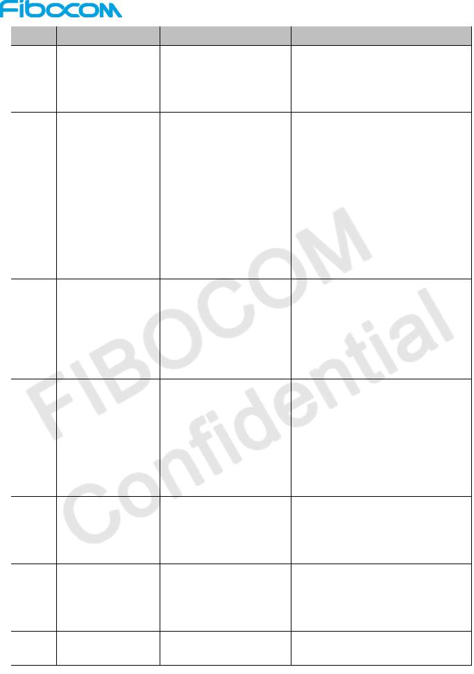
3.1.2 Pin definition
The pin definitions are shown in the following table: |
|
||||
Pin |
Pin Name |
I/O |
Level |
Description |
|
|
|
|
VILmin=-0.3V |
|
|
1 |
WAKEUP_IN |
I |
VILmax=0.6V |
External device wake-up module |
|
VIHmin=1.2V |
|||||
|
|
|
|
||
|
|
|
VIHmax=2.0V |
|
|
|
|
|
VILmin=-0.3V |
|
|
2 |
AP_READY |
I |
VILmax=0.6V |
Reserved |
|
VIHmin=1.2V |
|||||
|
|
|
|
||
|
|
|
VIHmax=2.0V |
|
|
3 |
RESERVED |
|
- |
Reserved |
|
|
|
|
VILmin=-0.3V |
|
|
4 |
W_DISABLE# |
I |
VILmax=0.6V |
Module flight mode control |
|
VIHmin=1.2V |
|||||
|
|
|
|
||
|
|
|
VIHmax=2.0V |
|
|
5 |
NET_MODE |
O |
VOHmin=1.35V |
Module state indicate |
|
VOLmax=0.45V |
|||||
|
|
|
|
||
6 |
NET_STATUS |
O |
VOHmin=1.35V |
Reserved |
|
VOLmax=0.45V |
|||||
|
|
|
|
||
7 |
VDD_EXT |
PO |
1.8V |
Module digital level, 1.8V output, 80mA |
|
8 |
GND |
G |
- |
Ground |
|
9 |
GND |
G |
- |
Ground |
|
10 |
GND |
G |
- |
Ground |
|
|
|
|
VILmin=-0.3V |
|
|
11 |
DBG_RXD |
I |
VILmax=0.6V |
DEBUG serial port Receive data |
|
VIHmin=1.2V |
|||||
|
|
|
|
||
|
|
|
VIHmax=2.0V |
|
|
12 |
DBG_TXD |
O |
VOLmax=0.45V |
DEBUG serial port Transmit data |
|
VOHmin=1.35V |
|||||
|
|
|
|
||
|
|
|
VILmin=-0.3V |
|
|
13 |
USIM_PRESENCE |
I |
VILmax=0.6V |
USIM card hot plug detection |
|
VIHmin=1.2V |
|||||
|
|
|
|
||
|
|
|
VIHmax=2.0V |
|
|
|
|
|
For 1.8V USIM: |
|
|
14 |
USIM _VDD |
O |
Vmax=1.9V |
USIM power |
|
|
|
|
Vmin=1.7V |
|
|
Reproduction forbidden without Fibocom Wireless Inc. written authorization - All Rights Reserved.
FIBOCOM NL668-AM Hardware User Manual |
Page 17 of 62 |
Pin |
Pin Name |
I/O |
Level |
Description |
|
|
|
|
For 3.0V USIM: |
|
|
|
|
|
Vmax=3.05V |
|
|
|
|
|
Vmin=2.7V |
|
|
|
|
|
IOmax=150mA |
|
|
|
|
|
For 1.8V USIM: |
|
|
|
|
|
VILmax=0.6V |
|
|
|
|
|
VIHmin=1.2V |
|
|
|
|
|
VOLmax=0.45V |
|
|
15 |
USIM _DATA |
O |
VOHmin=1.35V |
USIM data signal cable |
|
For 3.0V USIM: |
|||||
|
|
|
|
||
|
|
|
VILmax=1.0V |
|
|
|
|
|
VIHmin=1.95V |
|
|
|
|
|
VOLmax=0.45V |
|
|
|
|
|
VOHmin=2.55V |
|
|
|
|
|
For 1.8V USIM: |
|
|
|
|
|
VOLmax=0.45V |
|
|
16 |
USIM _CLK |
O |
VOHmin=1.35V |
USIM clock signal cable |
|
For3.0V USIM: |
|||||
|
|
|
|
||
|
|
|
VOLmax=0.45V |
|
|
|
|
|
VOHmin=2.55V |
|
|
|
|
|
For 1.8V USIM: |
|
|
|
|
|
VOLmax=0.45V |
|
|
17 |
USIM _RST |
O |
VOHmin=1.35V |
USIM reset signal cable |
|
For 3.0V USIM: |
|||||
|
|
|
|
||
|
|
|
VOLmax=0.45V |
|
|
|
|
|
VOHmin=2.55V |
|
|
18 |
NC |
- |
- |
NC |
|
19 |
GND |
G |
- |
Ground |
|
|
|
|
VIHmax=2.1V |
Module reset signal, active low, no |
|
20 |
RESET_N |
I |
VIHmin=1.3V |
||
need pull up externally |
|||||
|
|
|
VILmax=0.5V |
||
|
|
|
|
||
|
|
|
VIHmax=2.1V |
Turn on/off the module, active low, no |
|
21 |
PWRKEY |
I |
VIHmin=1.3V |
||
need pull up externally |
|||||
|
|
|
VILmax=0.5V |
||
|
|
|
|
||
22 |
GND |
G |
- |
Ground |
|
23 |
SD_INS_DET |
I |
- |
Reserved |
|
24 |
PCM_IN |
I |
VILmin=-0.3V |
PCM input signal |
|
|
Reproduction forbidden without Fibocom Wireless Inc. written authorization - All Rights Reserved. |
||||
FIBOCOM NL668-AM Hardware User Manual |
|
Page 18 of 62 |
|||

Pin |
Pin Name |
I/O |
Level |
Description |
|
|
|
|
VILmax=0.6V |
|
|
|
|
|
VIHmin=1.2V |
|
|
|
|
|
VIHmax=2.0V |
|
|
25 |
PCM_OUT |
O |
VOLmax=0.45V |
PCM output signal |
|
VOHmin=1.35V |
|||||
|
|
|
|
||
|
|
|
VOLmax=0.45V |
|
|
|
|
|
VOHmin=1.35V |
|
|
26 |
PCM_SYNC |
I/O |
VILmin=-0.3V |
PCM synchronization signal |
|
VILmax=0.6V |
|||||
|
|
|
|
||
|
|
|
VIHmin=1.2V |
|
|
|
|
|
VIHmax=2.0V |
|
|
|
|
|
VOLmax=0.45V |
|
|
|
|
|
VOHmin=1.35V |
|
|
27 |
PCM_CLK |
I/O |
VILmin=-0.3V |
PCM clock signal |
|
VILmax=0.6V |
|||||
|
|
|
|
||
|
|
|
VIHmin=1.2V |
|
|
|
|
|
VIHmax=2.0V |
|
|
28 |
SDC2_DATA3 |
I/O |
- |
Reserved |
|
29 |
SDC2_DATA2 |
I/O |
- |
Reserved |
|
30 |
SDC2_DATA1 |
I/O |
- |
Reserved |
|
31 |
SDC2_DATA0 |
I/O |
- |
Reserved |
|
32 |
SDC2_CLK |
O |
- |
Reserved |
|
33 |
SDC2_CMD |
I/O |
- |
Reserved |
|
34 |
VDD_SDIO |
PO |
- |
Reserved |
|
35 |
ANT_DIV |
I |
- |
Diversity antenna |
|
36 |
GND |
G |
- |
Ground |
|
37 |
SPI_CS_N |
I |
- |
Reserved |
|
38 |
SPI_MOSI |
I |
- |
Reserved |
|
39 |
SPI_MISO |
O |
- |
Reserved |
|
40 |
SPI_CLK |
O |
- |
Reserved |
|
41 |
I2C_SCL |
OD |
- |
I2C interface clock signal |
|
42 |
I2C_SDA |
OD |
- |
I2C interface data signal |
|
43 |
NC |
- |
- |
NC |
|
44 |
ADC1 |
I |
- |
Analog to digital converter interface |
|
45 |
ADC0 |
I |
- |
Analog to digital converter interface 0 |
|
46 |
GND |
G |
- |
Ground |
|
|
Reproduction forbidden without Fibocom Wireless Inc. written authorization - All Rights Reserved. |
||||
FIBOCOM NL668-AM Hardware User Manual |
|
Page 19 of 62 |
|||
 Loading...