

Page 1

690- 0502273076 www.fangtek.com
1
ft690
2W Mono BTL Audio Power Amplifier
General Description
The ft690 is an audio power amplifier primarily designed
for demanding applications in mobile phones and other
portable communication device applications. It is capable
of delivering 1.25 watts of continuous average power to
an 8Ω BTL load and 2 watts of continuous average
power (DFN only) to a 4Ω BTL load with less than 1%
distortion (THD+N+N) from a 5VDC power supply.
The ft690 was designed specifically to provide high
quality output power with a minimal amount of external
components. The ft690 does not require output coupling
capacitors or bootstrap capacitors, and therefore is ideally
suited for mobile phone and other low voltage
applications where minimal power consumption is a
primary requirement.
The ft690 features a low-power consumption shutdown
mode. To facilitate this, Shutdown may be enabled by
either logic high or low depending on mode selection.
Driving the shutdown mode pin either high or low
enables the shutdown pin to be driven in a likewise
manner to enable shutdown.
The ft690 contains advanced pop & click circuitry which
eliminates noise which would otherwise occur during
turn-on and turn-off transitions.
The ft690 is unity-gain stable and can be configured by
external gain-setting resistors.
Key Specifications
Improved PSRR at 217Hz & 1KHz 66dB
Power Output at 5.0V, 1% THD+N, 4Ω (QFN only)
2W (typ)
Power Output at 5.0V, 1% THD+N, 8Ω 1.25W (typ)
Power Output at 3.0V, 1% THD+N, 4Ω 600mW (typ)
Power Output at 3.0V, 1% THD+N, 8Ω 425mW (typ)
Shutdown Current 0.1μA (typ)
Features
Available in space-saving packages: DFN, MSOP,
WCSP
Ultra low current shutdown mode
Improved pop & click circuitry eliminates noise during
turn-on and turn-off transitions
2.2 - 5.5V operation
No output coupling capacitors, snubber networks or
bootstrap capacitors required
Unity-gain stable
External gain configuration capability
User selectable shutdown High or Low logic Level
Applications
Mobile Phones
PDAs
Portable electronic device
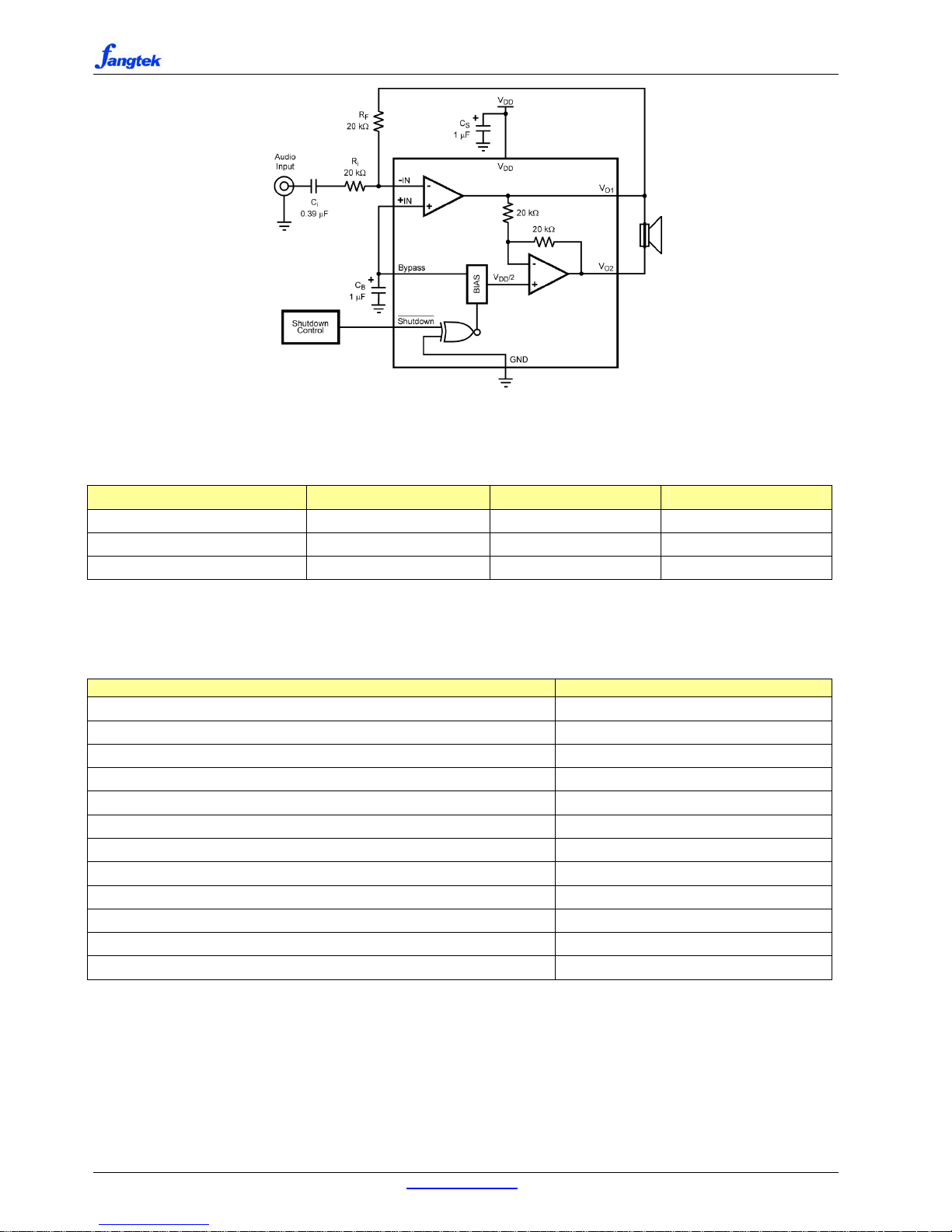
Application Circuit
Figure 1.Typical Audio Amplifier Application Circuit (DFN)
Doc# ft690- 0502273076
December 15, 2006
平网-功率器件专业供应商 0755-83307717 www.ping-web.com sales@ping-web.com
.
Page 2
ft690_DS_2.1
2 www.fangtek.com ft690- 0502273076
Figure 2.Typical Audio Amplifier Application Circuit (MSOP and WCSP)
ORDERING INFORMATION
P/N TEMP RANGE PIN-PACKAGE GAIN(dB)
ft690D
-40°C to +85°C 10pin DFN Adj.
ft690M
-40°C to +85°C 8pin MSOP Adj.
Ft690W
-40°C to +85°C 9pin WCSP Adj.
Ordering Information continued at end of data sheet.
Pin Configurations and Selector Guide appear at end of data sheet.
ABSOLUTE MAXIMUM RATINGS
Unit
Supply voltage, VDD 6.0 V
Storage Temperature −65°C to +150°C
Input Voltage −0.3V to VDD +0.3V
Power Dissipation Internally Limited
ESD Susceptibility 2000V
Junction Temperature 150°C
θJC (MSOP) 56°C/W
θJA (MSOP) 190°C/W
θJC (WCSP) 180°C/W
θJA (DFN) 63°C/W
θJC (DFN) 12°C/W
Lead temperature 1,6 mm (1/16 Inch) from case for 10 seconds 260°C
平网-功率器件专业供应商 0755-83307717 www.ping-web.com sales@ping-web.com
.
Page 3

ft690_DS_2.1
ft690- 0502273076 www.fangtek.com 3
RECOMMENDED OPERATING CONDITIONS
MIN YP MAX UNIT
Supply voltage, VDD 2.5 5.5 V
High-level input voltage, VIH SHUTDOWN 2 V
Low-level input voltage, VIL SHUTDOWN 0.8 V
Common-mode input voltage, VIC VDD = 2.5 V, 5.5 V, CMRR ≤ -60 dB 0.5 VDD-0.8 V
Operating free-air temperature, TA -40 85 °C
Load impedance, ZL 6.4 8
Ω
ELECTRICAL CHARACTERISTICS
VDD=5V TA=25°C
Symbol Parameter Conditions Typical Limit Units(Limits)
VIN=0V, IO=0A, No Load 2.5 7 mA (max)
IDD Quiescent Power Supply Current
VIN=0V, IO=0A, 8 Ω Load 3 10 mA (max)
ISD Shutdown Current VSD= V
SD MODE
(WCSP only)
0.1 2.0 μA (max)
V
SDIH
Shutdown Voltage Input High V
SD MODE
= VDD 1.5 V
V
SDIL
Shutdown Voltage Input Low V
SD MODE
= VDD 1.3 V
V
SDIH
Shutdown Voltage Input High V
SD MODE
= GND 1.5 V
V
SDIL
Shutdown Voltage Input Low V
SD MODE
= GND 1.3 V
VOS Output Offset Voltage 7 50 mV (max)
9.7 K Ω (max)
R
OUT
Resistor Output to GND 8.5
7.0 K Ω (min)
Output Power (8 Ω) THD+N=1% (max); f=1kHz 1.25 0.9 W (min)
PO
(4Ω) THD+N=1% (max); f=1kHz 2 W
TWU Wake-up time 130 Ms
THD+N Total Harmonic Distortion+Noise PO = 0.5Wrms; f=1kHz 0.2 %
PSRR Power Supply Rejection Ratio
V
ripple
=200mV sine p-p
Input terminated with 10 Ω
66(f=217Hz)
76(f=1kHz)
55 dB (min)
V
DD
=3V TA=25°C
Symbol Parameter Conditions Typical Limit Units(Limits)
VIN=0V, IO=0A, No Load 1.6 7 mA (max)
IDD Quiescent Power Supply Current
V
IN
=0V, IO=0A, 8 Ω Load 2 9 mA (max)
ISD Shutdown Current VSD= V
SD MODE
(WCSP only)
0.1 2.0 μA (max)
V
SDIH
Shutdown Voltage Input High V
SD MODE
= VDD 1.1 V
V
SDIL
Shutdown Voltage Input Low V
SD MODE
= VDD 0.9 V
V
SDIH
Shutdown Voltage Input High V
SD MODE
= GND 1.3 V
V
SDIL
Shutdown Voltage Input Low V
SD MODE
= GND 1.0 V
VOS Output Offset Voltage 7 50 mV (max)
9.7 K Ω (max)
R
OUT
Resistor Output to GND 8.5
7.0 K Ω (min)
Output Power (8 Ω) THD+N=1% (max); f=1kHz 425 mW
PO
Output Power (4 Ω) THD+N=1% (max); f=1kHz 600 mW
TWU Wake-up time 80 Ms
THD+N Total Harmonic Distortion+Noise PO = 0.25Wrms; f=1kHz 0.1 %
PSRR Power Supply Rejection Ratio
V
ripple
=200mV sine p-p
Input terminated with 10 Ω
66(f=217Hz)
76(f=1kHz)
55 dB (min)
平网-功率器件专业供应商 0755-83307717 www.ping-web.com sales@ping-web.com
.
Page 4

ft690_DS_2.1
4 www.fangtek.com ft690- 0502273076
VDD=2.6V TA=25°C
Symbol Parameter Conditions Typical Limit Units(Limits)
VIN=0V, IO=0A, No Load 1.5 mA (max)
IDD Quiescent Power Supply Current
VIN=0V, IO=0A, 8 Ω Load 2 mA (max)
ISD Shutdown Current VSD= V
SD MODE
(WCSP only) 0.1 μA (max)
V
SDIH
Shutdown Voltage Input High V
SD MODE
= VDD 1.0 V
V
SDIL
Shutdown Voltage Input Low V
SD MODE
= VDD 0.9 V
V
SDIH
Shutdown Voltage Input High V
SD MODE
= GND 1.2 V
V
SDIL
Shutdown Voltage Input Low V
SD MODE
= GND 1.0 V
VOS Output Offset Voltage 5 50 mV (max)
9.7 K Ω (max)
R
OUT
Resistor Output to GND 8.5
7.0 K Ω (min)
Output Power (8 Ω) THD+N=1% (max); f=1kHz 300 mW
PO
Output Power (4 Ω) THD+N=1% (max); f=1kHz 400 mW
TWU Wake-up time 70 Ms
THD+N+N Total Harmonic Distortion+Noise PO = 0.15Wrms; f=1kHz 0.1 %
PSRR Power Supply Rejection Ratio
V
ripple
=200mV sine p-p
Input terminated with 10 Ω
66(f=217Hz)
76(f=1kHz)
55 dB (min)
PIN DESCRIPTION
DFN Package
MSOP Package
Top View
Order Number ft690D
Top View
Order Number ft690M
WCSP Package
Top View
Order Number ft690W
平网-功率器件专业供应商 0755-83307717 www.ping-web.com sales@ping-web.com
.
Page 5

ft690_DS_2.1
ft690- 0502273076 www.fangtek.com 5
Package DFN MSOP WCSP
Shutdown Mode Selectable Low Low
Typical Power Output at 5V,
1% THD+N
2W (R
L
=4)
1.25W (RL=8Ω)
1.25W (RL=8)
A SD_MODE select pin determines the Shutdown Mode for the DFN package, whether it is an Asserted High or an Asserted Low device,
to activate shutdown.
The SD_MODE select pin is with the MSOP and WCSP packaged devices, shutdown occurs only with an low assertion.
Typical Performance Characteristics
LD and MH Specific Characteristics
THD+N+N vs Frequency
Vdd=5V, RL=8Ω, Po=0.5W
0.01
0.1
1
10
10 100 1000 10000 100000
Frequency (Hz)
THD+N (%)
THD+N+ N vs Fre quency
Vdd=3V, RL=8Ω, Po=0.25 W
0.01
0.1
1
10
10 100 1000 10000 100000
Frequency (Hz)
THD+N (%)
平网-功率器件专业供应商 0755-83307717 www.ping-web.com sales@ping-web.com
.
Page 6

ft690_DS_2.1
6 www.fangtek.com ft690- 0502273076
THD+N+ N vs Output P ow er
Vdd=5V, RL=8Ω, f= 1 KHz
0.01
0.1
1
10
0.01 0.1 1 10
Output Power (W)
THD+N (%)
THD+N+N vs Output P ow er
Vdd=3V, RL=8Ω, f=1KHz
0.01
0.1
1
10
0.01 0.1 1
Output Power (W)
THD+N (%)
THD+N+N vs Fre quency
Vdd=2.6V, RL=8Ω, Po=0.15W
0.01
0.1
1
10
10 100 1000 10000 100000
Fr e q ue n c y ( H z)
THD+N (%)
平网-功率器件专业供应商 0755-83307717 www.ping-web.com sales@ping-web.com
.
Page 7

ft690_DS_2.1
ft690- 0502273076 www.fangtek.com 7
THD+N+N vs Out put Pow er
Vdd=2 .6V, RL=8Ω, f= 1KHz
0.01
0.1
1
10
0.01 0.1 1
Output Powe r (W)
THD+N (%)
PSRR vs Frequenc y
Vdd=5V, RL=8Ω, Input=10Ω
-100
-90
-80
-70
-60
-50
-40
-30
-20
-10
0
10 100 1000 10000 100000
Frequency (Hz)
PSRR (dB)
PSRR vs Frequency
Vdd=3V, RL=8Ω, Input=10Ω
-100
-90
-80
-70
-60
-50
-40
-30
-20
-10
0
10 100 1000 10000 100000
Frequency (Hz)
PSRR (dB)
PSRR vs Frequency
Vdd=2.6V, RL=8Ω, Input=10Ω
-100
-90
-80
-70
-60
-50
-40
-30
-20
-10
0
10 100 1000 10000 100000
Frequency (Hz)
PSRR (dB)
Power Dissipation vs Output Power
Vdd=5V, RL=8
Ω
0
0.2
0.4
0.6
0.8
1
0 0.5 1 1.5 2
Output Power (W)
Power Dissipation (W)
平网-功率器件专业供应商 0755-83307717 www.ping-web.com sales@ping-web.com
.
Page 8

ft690_DS_2.1
8 www.fangtek.com ft690- 0502273076
Power Dissipation vs Output Power
Vdd=3V, RL=8
Ω
0
0.05
0.1
0.15
0.2
0.25
0.3
0.35
0.4
00.20.40.60.8
Output Power (W)
Power Dissipation (W)
Power Dissipation vs Output Powe r
Vdd=2.6V, RL=8
Ω
0
0.05
0.1
0.15
0.2
0.25
0.3
0 0.1 0.2 0.3 0.4 0.5
Output Power (W)
Power Dissipation (W)
Frequency Response vs Input Capacitor Size
Vdd=5 V, RL=8Ω, Cap=0.44uF
-10
-9
-8
-7
-6
-5
-4
-3
-2
-1
0
1
10 100 1000 10000 100000
Frequency (Hz)
Output Level (dB)
平网-功率器件专业供应商 0755-83307717 www.ping-web.com sales@ping-web.com
.
Page 9

ft690_DS_2.1
ft690- 0502273076 www.fangtek.com 9
Application Information
BRIDGE CONFIGURATION EXPLANATION
As shown in Figure 1, the ft690 has two internal
operational amplifiers. The first amplifier’s gain is
externally configurable, while the second amplifier is
internally fixed in a unity-gain, inverting configuration.
The closed-loop gain of the first amplifier is set by
selecting the ratio of R
f
to Ri while the second amplifier’s
gain is fixed by the two internal 20kΩ resistors. Figure 1
shows that the output of amplifier one serves as the input
to amplifier two which results in both amplifiers
producing signals identical in magnitude, but out of
phase by 180°. Consequently, the differential gain for the
IC is
A
VD
= 2 *(Rf/Ri)
By driving the load differentially through outputs Vo1
and Vo2, an amplifier configuration commonly referred
to as “bridged mode” is established. Bridged mode
operation is different from the classical single-ended
amplifier configuration where one side of the load is
connected to ground.
A bridge amplifier design has a few distinct advantages
over the single-ended configuration, as it provides
differential drive to the load, thus doubling output swing
for a specified supply voltage. Four times the output
power is possible as compared to a single-ended
amplifier under the same conditions. This increase in
attainable output power assumes that the amplifier is not
current limited or clipped. In order to choose an
amplifier’s closed-loop gain without causing excessive
clipping, please refer to Audio Power Amplifier Design
section.
A bridge configuration, such as the one used in ft690,
also creates a second advantage over single-ended
amplifiers. Since the differential outputs, Vo1 and Vo2,
are biased at half-supply, no net DC voltage exists across
the load. This eliminates the need for an output coupling
capacitor which is required in a single supply,
single-ended amplifier configuration. Without an output
coupling capacitor, the half-supply bias across the load
would result in both increased internal IC power
dissipation and also possible loudspeaker damage.
POWER DISSIPATION
Power dissipation is a major concern when designing a
successful amplifier, whether the amplifier is bridged or
single-ended. A direct consequence of the increased
power delivered to the load by a bridge amplifier is an
increase in internal power dissipation. Since the ft690 has
two operational amplifiers in one package, the maximum
internal power dissipation is 4 times that of a
single-ended amplifier. The maximum power dissipation
for a given application can be derived from the power
dissipation graphs or from Equation 1.
P
DMAX
= 4*(VDD)2/(2π2RL) (1)
It is critical that the maximum junction temperature
T
JMAX
of 150°C is not exceeded. T
JMAX
can be
determined from the power derating curves by using
P
DMAX
and the PC board foil area. By adding copper foil,
the thermal resistance of the application can be reduced
from the free air value of θ
JA
, resulting in higher P
DMAX
values without thermal shutdown protection circuitry
being activated. Additional copper foil can be added to
any of the leads connected to the ft690. It is especially
effective when connected to V
DD
, GND, and the output
pins. Refer to the application information on the ft690
reference design board for an example of good heat
sinking. If T
JMAX
still exceeds 150°C, then additional
changes must be made. These changes can include
reduced supply voltage, higher load impedance, or
reduced ambient temperature. Internal power dissipation
is a function of output power.
POWER SUPPLY BYPASSING
As with any amplifier, proper supply bypassing is critical
for low noise performance and high power supply
rejection. The capacitor location on both the bypass and
power supply pins should be as close to the device as
possible. Typical applications employ a 5V regulator
with 10μF tantalum or electrolytic capacitor and a
ceramic bypass capacitor which aid in supply stability.
This does not eliminate the need for bypassing the supply
nodes of the ft690. The selection of a bypass capacitor,
especially C
B
, is dependent upon PSRR requirements,
click and pop performance, system cost, and size
constraints.
SHUTDOWN FUNCTION
In order to reduce power consumption while not in use,
the ft690 contains shutdown circuitry that is used to turn
off the amplifier’s bias circuitry. In addition, the ft690
contains a Shutdown Mode pin (DFN only), allowing the
designer to designate whether the part will be driven into
shutdown with a high level logic signal or a low level
logic signal. This allows the designer maximum
flexibility in device use, as the Shutdown Mode pin may
simply be tied permanently to either VDD or GND to set
the ft690 as either a "shutdown-high" device or a
"shutdown-low" device, respectively. The device may
then be placed into shutdown mode by toggling the
Shutdown pin to the same state as the Shutdown Mode
pin. For simplicity’s sake, this is called "shutdown same",
as the ft690 enters shutdown mode whenever the two
pins are in the same logic state. The MSOP package
lacks this Shutdown Mode feature, and is permanently
fixed as a ‘Shutdown-low’ device. It is best to switch
between ground and supply for maximum performance.
While the device may be disabled with shutdown
voltages in between ground and supply, the idle current
平网-功率器件专业供应商 0755-83307717 www.ping-web.com sales@ping-web.com
.
Page 10

ft690_DS_2.1
10 www.fangtek.com ft690- 0502273076
may be greater than the typical value of 0.1μA. In either
case, the shutdown pin should be tied to a definite
voltage to avoid unwanted state changes.
In many applications, a microcontroller or
microprocessor output is used to control the shutdown
circuitry, which provides a quick, smooth transition to
shutdown. Another solution is to use a single-throw
switch in conjunction with an external pull-up resistor (or
pull-down, depending on shutdown high or low
application). This scheme guarantees that the shutdown
pin will not float, thus preventing unwanted state
changes.
PROPER SELECTION OF EXTERNAL
COMPONENTS
Proper selection of external components in applications
using integrated power amplifiers is critical to optimize
device and system performance. While the ft690 is
tolerant of external component combinations,
consideration to component values must be used to
maximize overall system quality.
The ft690 is unity-gain stable which gives the designer
maximum system flexibility. The ft690 should be used in
low gain configurations to minimize THD+N+N values,
and maximize the signal to noise ratio. Low gain
configurations require large input signals to obtain a
given output power. Input signals equal to or greater than
1Vrms are available from sources such as audio codecs.
Please refer to the section, Audio Power Amplifier
Design, for a more complete explanation of proper gain
selection.
Besides gain, one of the major considerations is the
closed loop bandwidth of the amplifier. To a large extent,
the bandwidth is dictated by the choice of external
components shown in Figure 1. The input coupling
capacitor, C
i
, forms a first order high pass filter which
limits low frequency response. This value should be
chosen based on needed frequency response for a few
distinct reasons.
SELECTION OF INPUT CAPACITOR SIZE
Large input capacitors are both expensive and space
hungry for portable designs. Clearly, a certain sized
capacitor is needed to couple in low frequencies without
severe attenuation. But in many cases the speakers used
in portable systems, whether internal or external, have
little ability to reproduce signals below 100Hz to 150Hz.
Thus, using a large input capacitor may not increase
actual system performance.
In addition to system cost and size, click and pop
performance is effected by the size of the input coupling
capacitor, C
i
. A larger input coupling capacitor requires
more charge to reach its quiescent DC voltage (nominally
1/2 V
DD
). This charge comes from the output via the
feedback and is apt to create pops upon device enable.
Thus, by minimizing the capacitor size based on
necessary low frequency response, turn-on pops can be
minimized.
Besides minimizing the input capacitor size, careful
consideration should be paid to the bypass capacitor
value. Bypass capacitor, C
B
, is the most critical
component to minimize turn-on pops since it determines
how fast the ft690 turns on. The slower the ft690’s
outputs ramp to their quiescent DC voltage (nominally
1/2 V
DD
), the smaller the turn-on pop. Choosing CB
equal to 1.0μF along with a small value of C
i
(in the
range of 0.1μF to 0.39μF), should produce a virtually
clickless and popless shutdown function. While the
device will function properly, (no oscillations or
motorboating), with C
B
equal to 0.1μF, the device will be
much more susceptible to turn-on clicks and pops. Thus,
a value of C
B
equal to 1.0μF is recommended in all but
the most cost sensitive designs.
AUDIO POWER AMPLIFIER DESIGN
A 1W/8Ω Audio Amplifier
Given:
Power Output 1Wrms
Load Impedance 8Ω
Input Level 1Vrms
Input Impedance 20kΩ
Bandwidth 100Hz–20kHz ± 0.25dB
A designer must first determine the minimum supply rail
to obtain the specified output power. By extrapolating
from the Output Power vs Supply Voltage graphs in the
Typical Performance Characteristics section, the
supply rail can be easily found.
5V is a standard voltage in most applications, it is chosen
for the supply rail. Extra supply voltage creates
headroom that allows the ft690 to reproduce peaks in
excess of 1W without producing audible distortion. At
this time, the designer must make sure that the power
supply choice along with the output impedance does not
violate the conditions explained in the Power
Dissipation section.
Once the power dissipation equations have been
addressed, the required differential gain can be
determined from Equation 2.
(2)
R
f/Ri
= AVD/2
From Equation 2, the minimum A
VD
is 2.83; use AVD = 3.
Since the desired input impedance was 20kΩ, and with a
A
VD
impedance of 2, a ratio of 1.5:1 of Rf to Ri results in
an allocation of Ri = 20kΩ and Rf = 30kΩ. The final
design step is to address the bandwidth requirements
平网-功率器件专业供应商 0755-83307717 www.ping-web.com sales@ping-web.com
.
Page 11

ft690_DS_2.1
ft690- 0502273076 www.fangtek.com 11
which must be stated as a pair of −3dB frequency points.
Five times away from a −3dB point is 0.17dB down from
passband response which is better than the required
±0.25dB specified.
f
L
= 100Hz/5 = 20Hz
f
H
= 20kHz * 5 = 100kHz
R
i
in conjunction with Ci create a highpass filter.
C
i
≥ 1/(2π*20kΩ*20Hz) = 0.397μF; use 0.39μF
The high frequency pole is determined by the product of
the desired frequency pole, f
H
, and the differential gain,
AVD. With a AVD = 3 and fH = 100kHz, the resulting
GBWP = 300kHz which is much smaller than the ft690
GBWP of 2.5MHz. This figure displays that if a designer
has a need to design an amplifier with a higher
differential gain, the ft690 can still be used without
running into bandwidth limitations
Figure 3. HIGHER GAIN AUDIO AMPLIFIER
The ft690 is unity-gain stable and requires no external
components besides gain-setting resistors, an input
coupling capacitor, and proper supply bypassing in the
typical application. However, if a closed-loop differential
gain of greater than 10 is required, a feedback capacitor
(C4) may be needed as shown in Figure 2 to bandwidth
limit the amplifier. This feedback capacitor creates a low
pass filter that eliminates possible high frequency
oscillations. Care should be taken when calculating the
-3dB frequency in that an incorrect combination of R
3
and C4 will cause rolloff before 20kHz. A typical
combination of feedback resistor and capacitor that will
not produce audio band high frequency rolloff is R
3
=
20kΩ and C
4
= 25pf. These components result in a -3dB
point of approximately 320kHz.
Figure 4. DIFFERENTIAL AMPLIFIER CONFIGURATION FOR ft690
平网-功率器件专业供应商 0755-83307717 www.ping-web.com sales@ping-web.com
.
Page 12

ft690_DS_2.1
12 www.fangtek.com ft690- 0502273076
PHYSICAL DIMENSIONS
平网-功率器件专业供应商 0755-83307717 www.ping-web.com sales@ping-web.com
.
Page 13

ft690_DS_2.1
ft690- 0502273076 www.fangtek.com 13
Figure 5. DFN Package Physical Dimension
平网-功率器件专业供应商 0755-83307717 www.ping-web.com sales@ping-web.com
.
Page 14

ft690_DS_2.1
14 www.fangtek.com ft690- 0502273076
Figure 6. MSOP Package Physical Dimension
Figure 7. WCSP Package Physical Dimension
平网-功率器件专业供应商 0755-83307717 www.ping-web.com sales@ping-web.com
.
Page 15

ft690_DS_2.1
ft690- 0502273076 www.fangtek.com 15
IMPORTANT NOTICE
1. Disclaimer: The information in document is intended to help you evaluate this product. Fangtek, Inc. makes no warranty,
either expressed or implied, as to the product information herein listed, and reserves the right to change or discontinue work on
this product without notice.
2. LIFE SUPPORT POLICY: FANGTEK’S PRODUCTS ARE NOT AUTHORIZED FOR USE AS CRITICAL COMPONENTS IN
LIFE SUPPORT DEVICES OR SYSTEMS WITHOUT THE EXPRESS WRITTEN APPROVAL OF THE PRESIDENT AND
GENERAL COUNSEL OF FANGTEK INC. As used herein
Life support devices or systems are devices or systems which, (a) are intended for surgical implant into the body, or (b) support
or sustain life, and whose failure to perform when properly used in accordance with instructions for use provided in the labeling,
can be reasonably expected to result in a significant injury to the user.
A critical component is any component of a life support device or system whose failure to perform can be reasonably expected
to cause the failure of the life support device or system, or to affect its safety or effectiveness.
3. FANGTEK ASSUMES NO LIABILITY FOR INCIDENTAL, CONSEQUENTIAL OR SPECIAL DAMAGES OR INJURY THAT
MAY RESULT FROM MISAPPLICATIONS OR IMPROPER USE OR OPERATION OF ITS PRODUCTS
4. FANGTEK MAKES NO WARRANTY OR REPRESENTATION THAT ITS PRODUCTS ARE SUBJECT TO INTELLECTUAL
PROPERTY LICENSE FROM FANGTEK OR ANY THIRD PARTY, AND FANGTEK MAKES NO WARRANTY OR
REPRESENTATION OF NON-INFRINGEMENT WITH RESPECT TO ITS PRODUCTS. FANGTEK SPECIFICALLY
EXCLUDES ANY LIABILITY TO THE CUSTOMER OR ANY THIRD PARTY ARISING FROM OR RELATED TO THE
PRODUCTS’ INFRINGEMENT OF ANY THIRD PARTY’S INTELLECTUAL PROPERTY RIGHTS, INCLUDING PATENTS,
COPYRIGHT, TRADEMARK OR TRADE SECRET RIGHTS OF ANY THIRD PARTY.
5. THE INFORMATION IN THIS DOCUMENT IS MERELY TO INDICATE THE CHARACTERISTICS AND PERFORMANCE
OF FANGTEK PRODUCTS. FANGTEK ASSUMES NO RESPONSIBILITY FOR ANY INTELLECTUAL PROPERTY CLAIMS
OR OTHER PROBLEMS THAT MAY RESULT FROM APPLICATIONS BASED ON THE DOCUMENT PRESENTED HEREIN.
FANGTEK MAKES NO WARRANTY WITH RESPECT TO ITS PRODUCTS, EXPRESS OR IMPLIED, INCLUDING, BUT NOT
LIMITED TO THE WARRANTIES OF MERCHANTABILITY, FITNESS FOR A PARTICULAR USE AND TITLE.
6. Trademarks: The company and product names in this document may be the trademarks or registered trademarks of their
respective manufacturers. Fangtek is trademark of Fangtek, Inc.
CONTACT INFORMATION
20823 Stevens Creek Blvd,. N. 2/F., 2 Lane 690, Bibo Rd.
Suit 300 Cupertino, Zhangjiang Hi-tech Park, Pudong Dist.
CA 95014, USA Shanghai, China 201203
Tel: +1-408-996-1098 Tel: +86-21-5027-1868
Fax: +1-408-996-0339 Fax: +86-21-5027-1869
Email: info@fangtek.com Email: info@fangtek.com.cn
平网-功率器件专业供应商 0755-83307717 www.ping-web.com sales@ping-web.com
.
 Loading...