

Page 1
ft2925
CAVDD
1uF
EN
+
CPVOUT
220uF
VDD
CPVOUT
22uF
Cin
0.22uF
INNR
CVBAT
1uF
INPR
INNL
CPVOUT
0.1uF
CBVDD
0.1uF
CS
22uF
ft2925
2
3
4
5
6
7
8
10
12
13
14 15
16
17
18
9
1
19
20
11
21
22
23
24
25
26
27
28
INNL
INPL
PGND
VOPL
VONL
PVDDL
AVDD
NC
ALC
SDRIVE
EN LX
LX
PGNDB
PGNDB
BVDD
VBAT
PVOUT
PVOUT
VKNEE
PVSNS
PVDDR
VONR
VOPR
PGND
INPR
INNR
AGND
LSL
SPEAKER
INPL
Rin 15K
Cin 0.22uFCin 0.22uF
Rin
15K
Cin
0.22uF
RS2 10Ω
LSR
SPEAKER
CS
0.1uF
D1 SS34
CPVDDR
1uF PVDD
RS1 10Ω
L 3.3uH
VDD
Rin 15K
Rin
15K
PVDD
CPVDDL
1uF
2x6W Class-G Stereo Audio Power Amplifier
with Automatic Level Control & Battery Tracking AGC
GENERAL DESCRIPTION
The ft2925 is a highly efficient 2x6W Class-G stereo
audio power amplifier with automatic level control (ALC)
and battery tracking AGC. It integrates dual filterless
Class-D audio amplifiers with a multi-level Class-G
synchronous boost regulator and operates with a range
of supply voltages from 3V to 5.5V. When operating
with a 3.6V supply voltage, the ft2925 can deliver an
output power of 6W per channel with 10% THD+N, or
an ALC output power of 4.5W per channel with 0.3%
THD+N, into a pair of 4Ω speakers.
In ft2925, the power supply rails of the audio amplifiers’
output stages are internally boosted and regulated by a
synchronous PWM switching regulator with two
integrated power switches. The boost regulator
employs current-mode PWM control with proprietary
multi-level Class-G operation to regulate the boosted
output voltage dynamically in response to the voltage
level of the audio outputs.
The ft2925 features ALC function to constantly monitor
and safeguard the audio outputs against the boosted
supply voltages, preventing output clipping distortion,
excessive power dissipation, and speaker over-load.
Once an over-level condition is detected in either
channel, the ALC lowers the voltage gain of both audio
amplifiers together to limit the peak audio outputs.
In conjunction with ALC, as the battery supply voltage
drops below a prescribed value, the battery tracking
AGC lowers the voltage gain of both audio amplifiers to
limit the peak audio outputs, preventing the collapse of
battery voltage.
FEATURES
Wide range of supply voltages from 3V to 5.5V
Dual filterless Class-D audio amplifiers integrated
with a multi-level Class-G boost regulator
Automatic level control to eliminate output clipping
Battery tracking AGC to prevent battery collapse
Soft drive mode for EMI reduction
Maximum output power (Non-ALC Mode)
(VBAT=3.6V, ALC=High, THD+N=10%)
6.0W/Ch (4Ω Load)
3.5W/Ch (8Ω Load)
ALC output power (ALC Mode)
(VBAT=3.6V, ALC=Low, THD+N=0.3%)
4.5W/Ch (4Ω Load)
2.6W/Ch (8Ω Load)
Wide ALC dynamic range: 12dB
Maximum voltage gain: 30dB
High efficiency: 78%
(VBAT=3.6V, 4Ω Load, Po=2W/Ch, both channels driven)
Volume fade-in and fade-out
Under-voltage lockout protection
Auto-recovering over-current & short-circuit
protection
Thermal over-load protection
Available in TSSOP-28L package
APPLICATIONS
Blue Tooth Speakers
Portable Audio Decks
Consumer Audio Electronics
APPLICATION CIRCUIT
DEC, 2017 www.fangtek.com.cn 1
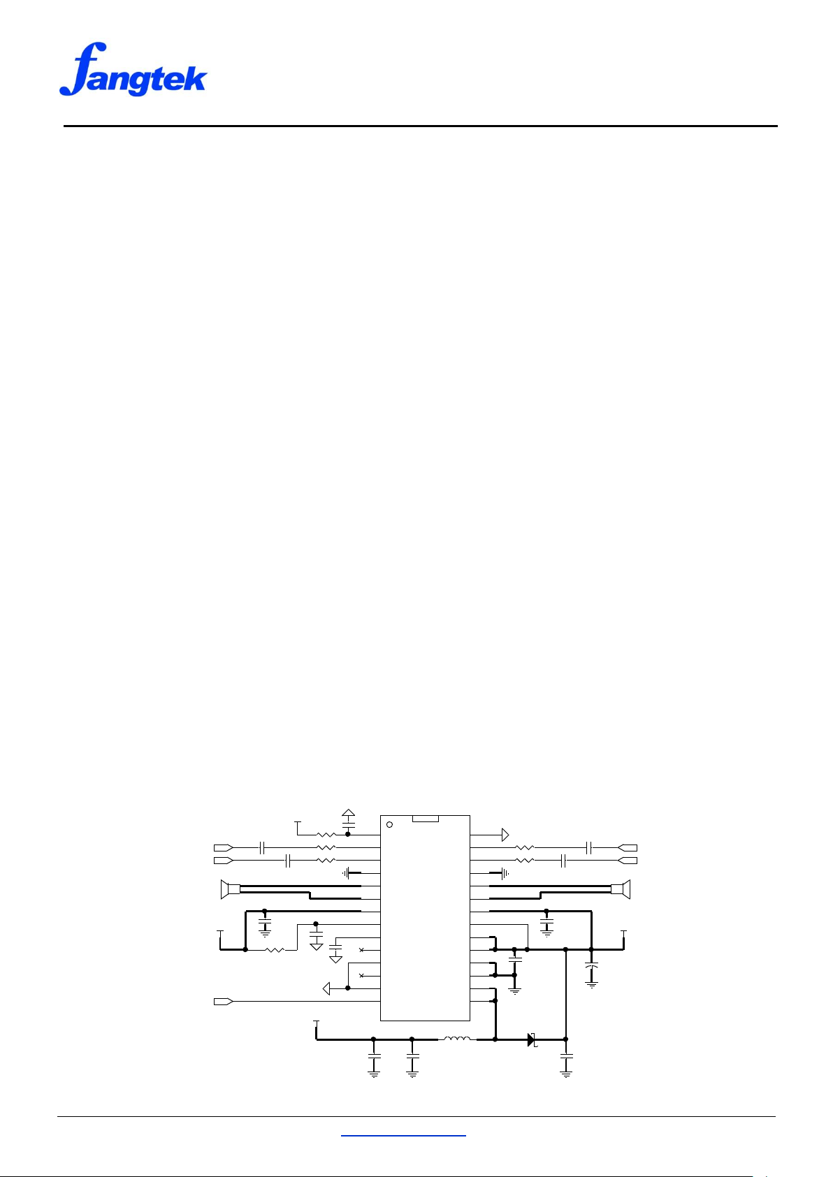
Figure 1: Typical Application Circuit Diagram of ft2925
Page 2
ft2925
NAME
PIN #
TYPE
DESCRIPTION
VBAT 1 P
Supply input voltage. Connect to a 1µF capacitor for decoupling. It is externally connected to
the system supply through a small decoupling resistor of 10Ω.
INNL 2 AI
Left-channel inverting audio input terminal.
INPL 3 AI
Left-channel non-inverting audio input terminal.
PGND 4 G
Power ground for the left-channel audio amplifier’s output stage.
VOPL 5 AO
Left-channel non-inverting audio output terminal.
VONL 6 AO
Left-channel inverting audio output terminal.
PVDDL 7 P
Power supply input for the left-channel audio amplifier’s output stage. Connect directly to the
output capacitor of PVOUT. Also, connect to a 1µF capacitor for decoupling.
AVDD 8 P
Boosted supply input voltage for internal circuitry. Connect it to a 1µF capacitor for decoupling.
Also, place a small decoupling resistor of 10Ω between this pin and PVOUT.
BVDD 9 AO
Internally generated voltage reference. Connect to a 0.1µF capacitor for decoupling.
VKNEE
11
DI
Battery Tracking AGC Control with an internal 300kΩ pullup resistor to VBAT and an internal
300kΩ pulldown resistor to ground.
ALC
12
DI
ALC Mode Control with an internal 300kΩ pullup resistor to VBAT and an internal 300kΩ
pulldown resistor to ground.
SDRIVE
13
DI
Soft Drive Control with an internal 300kΩ pullup resistor to VBAT and an internal 300kΩ
pulldown resistor to ground. When unconnected, the boost regulator is disabled.
EN
14
DI
Chip Enable (Active High) with an internal 300kΩ pulldown resistor to ground.
LX
15, 16
AO
Switch node of the boost regulator.
PGNDB
17, 18
G
Power ground for the boost regulator’s output stage.
PVOUT
19, 20
P
Boosted voltage output.
PVSNS
21
AI
Boosted voltage sense. Connect directly to the output capacitor of PVOUT.
PVDDR
22
P
Power supply input for the right-channel audio amplifier’s output stage. Connect directly to the
output capacitor of PVOUT. Also, connect to a 1µF capacitor for decoupling.
VONR
23
AO
Right-channel inverting audio output terminal.
VOPR
24
AO
Right-channel non-inverting audio output terminal.
PGND
25
G
Power ground for the right-channel audio amplifier’s output stage.
INPR
26
AI
Right-channel non-inverting audio input terminal.
INNR
27
AI
Right-channel inverting audio input terminal.
AGND
28
G
Analog ground.
NC
10
No internal connection.
PART NUMBER
TEMPERATURE RANGE
PACKAGE
ft2925P
-40°C to +85°C
TSSOP-28L
EN
19
18
INPR
22
9
VOPL
26
13
28
5
VBAT
PGNDB
21
LX
AGND
15
LX
7
INNL
4
6
PVSNS
PVDDL
20
INPL
8
3
23
16
PVOUT
1
27
PGNDB
PVDDR
ALC
VONR
12
AVDD
PGND
24 VOPR
10
PVOUT
NC
25
14
INNR
17
VONL
BVDD
VKNEE
SDRIVE
11
2
PGND
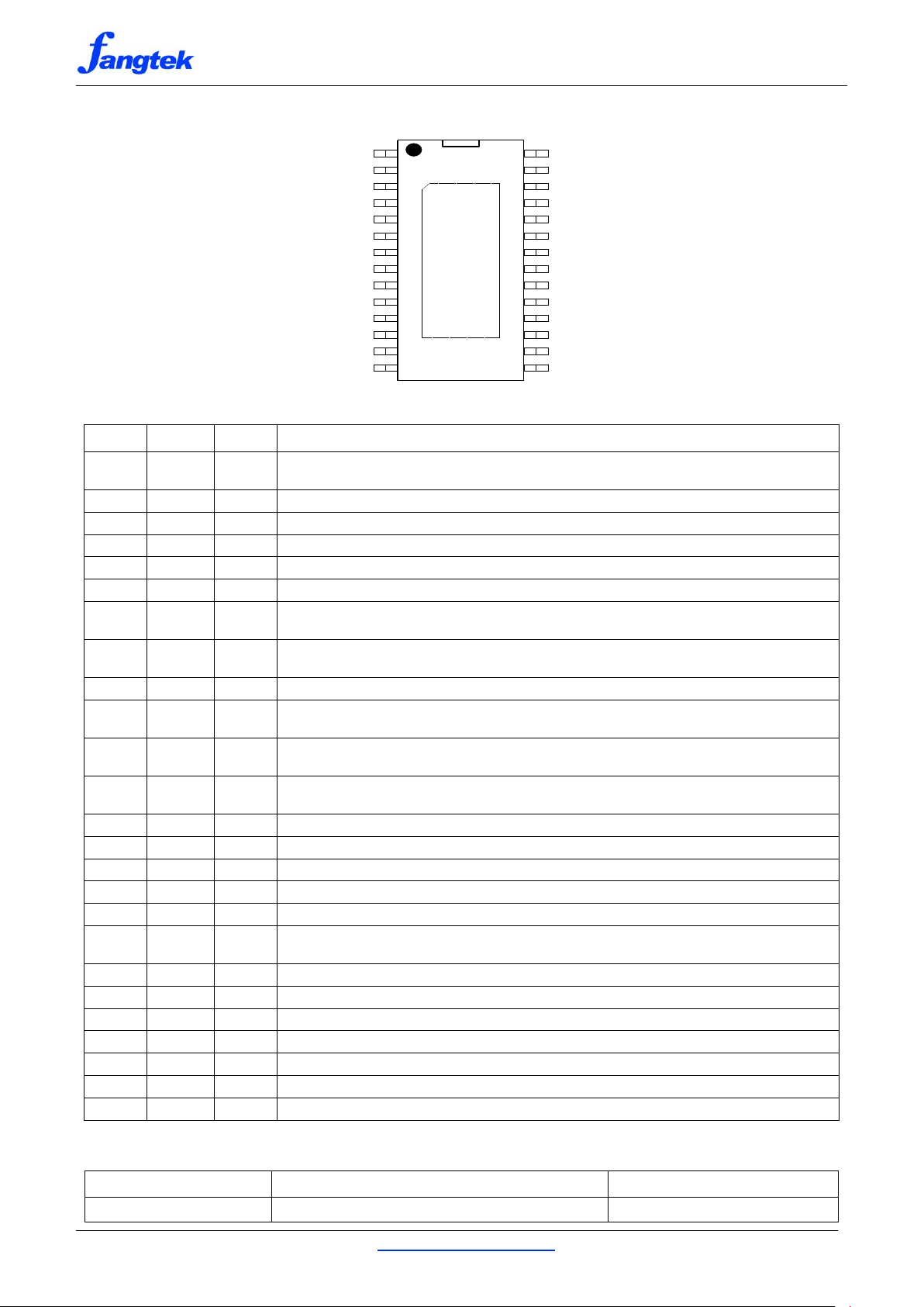
PIN CONFIGURATION AND DESCRIPTION
ft2925P (TOP VIEW)
ORDERING INFORMATION
DEC, 2017 http://www.fangtek.com.cn 2
Page 3
ft2925
PARAMETER
VALUE
Supply voltage, VBAT
-0.3V to 6V
LX, PVOUT, PVDDL/R, PVSNS, AVDD, VOPL/R, VONL/R
-0.3V to 8V
PGND, PGNDB
-0.3V to 0.3V
All other Pins
-0.3V to VBAT+0.3V
Storage Temperature
-65°C to +150°C
ESD Ratings-Human Body Model (HBM)
4000V
Junction Temperature
150°C
Maximum Soldering Temperature (@10 second duration)
260°C
PACKAGE
TA < +25°C
TA = +70°C
TA = +85°C
ΘJA
TSSOP-28L
4.5W
2.8W
2.3W
28°C/W
PARAMETER
SYMBOL
CONDITIONS
MIN
TYP
MAX
UNIT
Supply Voltage
VDD 3.0 5.5
V
Minimum Load Impedance
RL
Across VOPL/R & VONL/R
3.4 4
Ω
Audio Input Resistor
RIN
@ INPL/R, INNL/R
0 56
k
Ω
Audio Input Capacitor
CIN
@ INPL/R, INNL/R
0.1
0.22
1.0
µF
Boost Regulator Inductor
L 2.2
3.3
4.7
µH Boost Regulator Input Capacitor
CS
Ceramic
10
22 µ
F
Boost Regulator Output Capacitor
C
PVOUT
Ceramic
22
44 µF Electrolytic or Tantalum
(Note 4)
100
220 µF
BVDD Output Capacitor
CBVDD
0.1 µF
PVDD Decoupling Capacitors
CPVDDL/R
1 µF
Operating Junction Temperature
TJ -40 125
C
Ambient Temperature
TA -40 85
C
Operating Mode Control
SDRIVE
High η Drive, Boost regulator Enabled
Short to GND
Soft Drive, Boost regulator Disabled
Unconnected
Soft Drive, Boost regulator Enabled
Short to VBAT
ALC Mode Control
ALC
ALC-1
Short to GND
ALC-2
Unconnected
Non-ALC
Short to VBAT
Battery Tracking AGC Control
VKNEE
Battery Tracking AGC Disabled
Short to GND
VKNEE=3.15V
Unconnected
VKNEE=3.40V
Short to VBAT
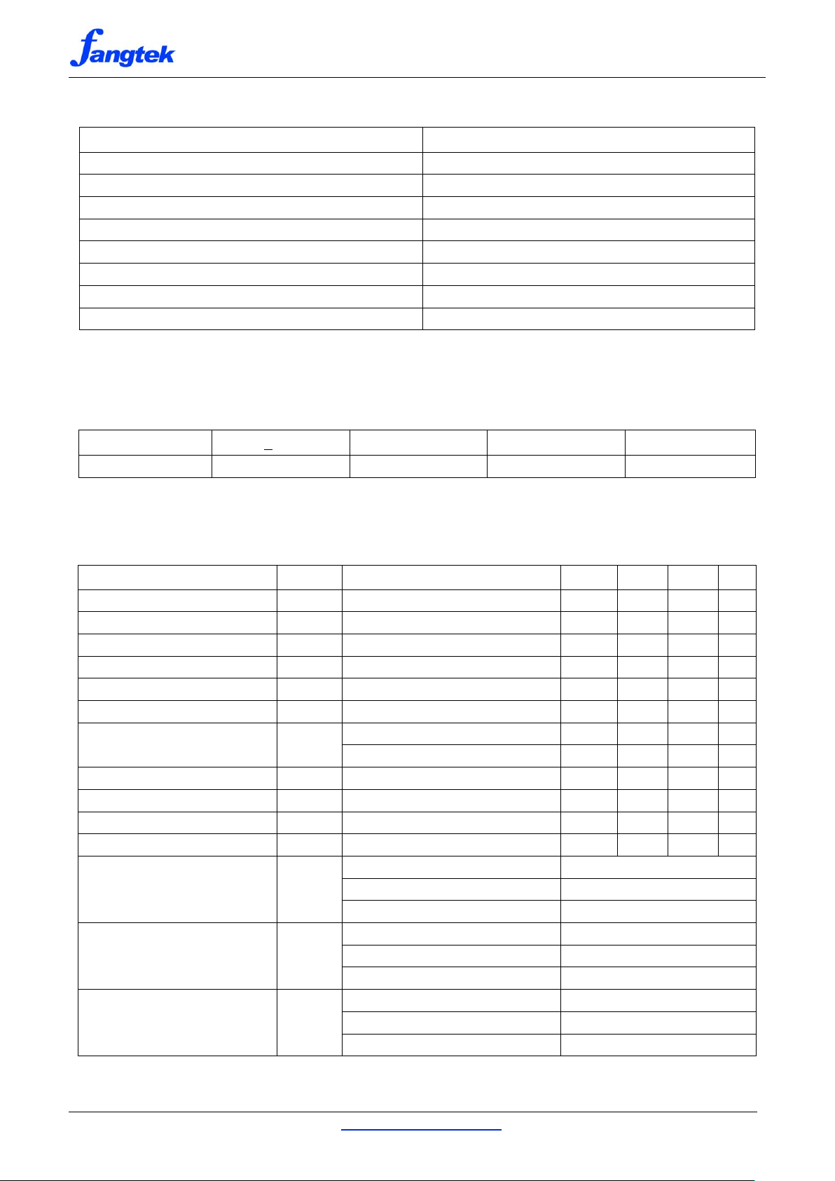
ABSOLUTE MAXIMUM RATINGS
Note 1: Stresses beyond those listed under absolute maximum ratings may cause permanent damage to the device. These are stress
ratings only, and functional operation of the device at any conditions beyond those indicated under recommended operating conditions is
not implied. Exposure to absolute-maximum-rated conditions for extended periods may also affect device reliability.
(Note1)
POWER DISSIPATION RATINGS
Note 2: The thermal pad of the package must be directly soldered onto a grounded metal island as a thermal sink on the system board.
Note 3: The power dissipation ratings are for a two-side, two-plane printed circuit board (PCB).
(Note 2, 3)
RECOMMENDED OPERATING CONDITIONS
Note 4: A bulk output capacitor (either electrolytic or tantalum) is typically added to facilitate higher voltage margin for higher audio power
at low frequencies. However, be cautious using any bulk output capacitance higher than 220µF as it might adversely slow the boost
regulator’s response to load transients to some extent affecting audio dynamics when playing music.
DEC, 2017 http://www.fangtek.com.cn 3
Page 4

ft2925
IMPORTANT APPLICATION NOTES
1. It is crucial to place the ft2925 in close proximity to the inductor, Schottky diode, and input/output capacitors
of the boost regulator on the system board, minimizing parasitic resistances and inductances of high-current
traces. Also, these passive components must be placed on the same layer with ft2925 and connected with
wide and short metal lines without vias. Failure to do a proper layout on the system board can result in
significant degradation of maximum output power, efficiency, THD, and EMI performance. It might even
induce excessive ringing at the switch node LX and damage the device permanently.
2. Use wide open areas on the top and bottom layers of the system board as the ground plane (GND) for ft2925.
Place lots of solid vias connecting the top and bottom layers of GND. Furthermore, for proper thermal
dissipation, reserve wide and uninterrupted GND areas along the thermal flow on the top layer, i.e., no wires
cutting through the GND layer and obstructing the thermal flow.
3. The ft2925 is packaged with an exposed thermal pad on the underside of the device. Solder the thermal pad
directly onto a large grounded metal island, as a thermal sink, underneath the package for proper thermal
dissipation. On the grounded metal island, place several rows of solid, equally-spaced vias connecting to the
bottom layer of GND. Failure to do so can severely limit its thermal dissipation capability. It might even cause
the device going into over-temperature shutdown occasionally.
4. All the ground pins (AGND, PGND and PGNDB) are directly connected to the ground plane (GND). The
power supply inputs (PVDDL/R) for the audio amplifiers’ output stages are directly connected to the output
capacitors of the boost regulator with wide and short metal traces.
5. As a high-performance Class-G stereo audio amplifier, the ft2925 requires adequate power supply
decoupling to ensure its high-efficiency, low distortion, and low EMI. Place each decoupling capacitor as
individually close to VBAT, AVDD, BVDD, and PVDDL/R pins as possible.
6. For best noise performance, use differential inputs from the audio sources for ft2925. In single-ended input
applications, the unused inputs of ft2925 should be AC-grounded at the audio source.
7. With an on-chip rectification power switch, the ft2925 requires no external Schottky diode for applications
where speaker load resistances are 8Ω. However, for applications where speaker load resistances are 4Ω or
less, it is required to add an auxiliary Schottky diode across LX and PVOUT pins to improve maximum output
power and overall power efficiency. The added Schottky diode must be rated for a current no less than 3A
and a reverse breakdown voltage no less than 15V.
8. Additional EMI suppression can be achieved using a ferrite bead filter constructed from a ferrite bead and a
capacitor, as shown in Figure 31. Choose a ferrite bead with a rated current no less than 1A for an 8Ω load
and 2A for a 4Ω load. Also, place the ferrite beard filter tightly together and individually close to VOPL/R and
VONL/R pins respectively.
9. Add a simple RC snubber circuit across two audio outputs (VOPL/R and VONL/R) for each channel, as
shown in Figure 32, to prevent the device from accelerated deterioration or abrupt destruction due to
excessive inductive flybacks that are induced on fast output switching or by an over-current condition.
10. The operation of the battery tracking AGC can be highly influenced by the electrical characteristics of the
battery. Place a small decoupling resistor of 10Ω between the battery supply voltage and the VBAT pin,
coupled with a decoupling capacitor of 1µF, mitigating the detrimental effect of high battery current ripples on
the detection of battery voltage.
11. Place a small decoupling resistor of 10Ω between AVDD and PVOUT pins, coupled with a decoupling
capacitor of 1µF, preventing high frequency transients from interfering with the on-chip linear amplifiers.
12. Use direct low-impedance traces for the audio outputs (VOPL/R and VONL/R) to the output filters and to the
speakers.
13. Do not connect any audio outputs (VOPL/R or VONL/R) directly to GND, PVOUT, or PVDDL/R as this might
damage the device permanently.
14. Do not alter the logic state of the SDRIVE pin while the device is in operation. To change the operating mode,
the device must be first placed in shutdown mode for a minimum of 100 milliseconds.
DEC, 2017 http://www.fangtek.com.cn 4
Page 5
ft2925
INNR
LX
ALC Control
BIAS
VONL
PVDDR
Class-D
Modulator
SDRIVE
Battery
Ttracking
AGND
VOPR
EN
VKNEE
AVDD
PVDDL
OTP
Output
Stage
VBAT
Class-D
Modulator
VONR
INPL
Input
Buffer
ALC
PVSNS
PVOUT
Boost
Battery
Monitor
PGND
PGND
BVDD
Output
Stage
INNL
Oscillator
INPR
PGNDB
OCP
Shutdown
Control
UVLO
VOPL
Input
Buffer
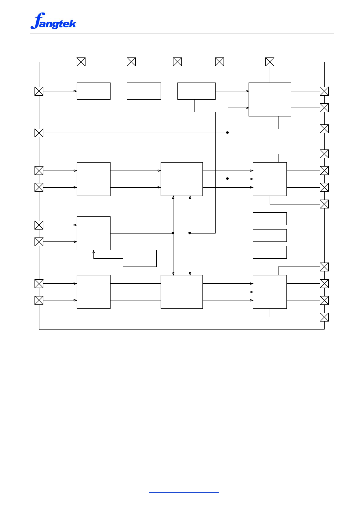
FUNCTIONAL BLOCK DIAGRAM
Figure 2: Simplified Functional Block Diagram of ft2925
DEC, 2017 http://www.fangtek.com.cn 5
Page 6
ft2925
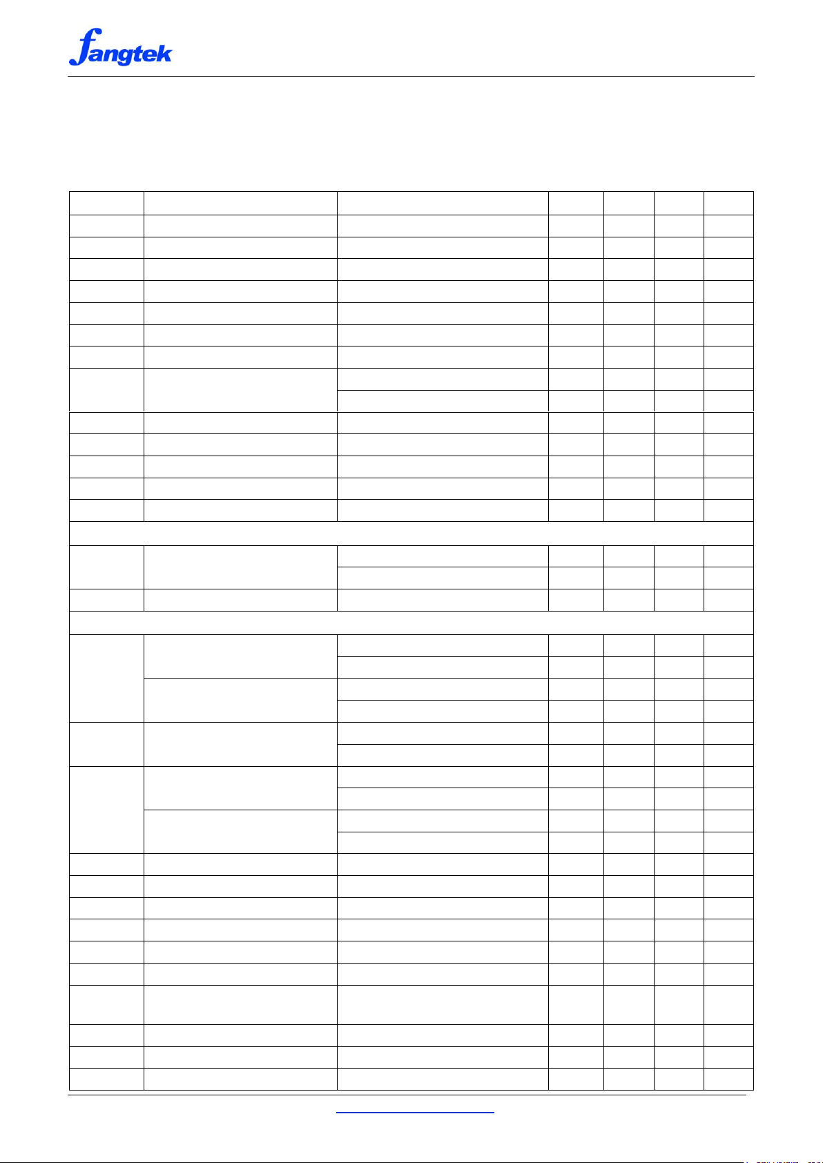
SYMBOL
PARAMETER
CONDITIONS
MIN
TYP
MAX
UNIT
VBAT
Supply Input Voltage
3.0 5.5
V
VUVLOUP
Power-on Threshold Voltage
VBAT from Low to High
2.2 V
VUVLODN
Power-off Threshold Voltage
VBAT from High to Low
2.0 V
IVBAT
Supply Quiescent Current
Inputs AC-Grounded, No Load
7
10
14
mA
IAVDD
Quiescent Current
VIN=0.25VRMS, No Load
6
mA
ISD
Shutdown Current
EN Low 1 µA
BVDD
Voltage Reference
Inputs AC-Grounded, No Load
3.0
3.2
3.4
V
VIH
Digital High Level Input Voltage
EN
1.2 V ALC, SDRIVE, VKNEE
VBAT-0.5
VBAT
V
VIL
Digital Low Level Input Voltage
EN, ALC, SDRIVE, VKNEE
0.4
V
RDOWN
Pulldown Resistor to Ground
EN, ALC, SDRIVE, VKNEE
300 kΩ
RUP
Pullup Resistor to VBAT
ALC, SDRIVE, VKNEE
300 kΩ
TOTSD
Over-Temperature Threshold
160
°C
THYS
Over-Temperature Hysteresis
20
°C
Class-G Boost Regulator
PVOUT
Boosted Voltage
No Load
7.0
7.2
7.4
V
ILOAD=1A
7.0 V
fBOOST
PWM Switching Frequency
800 kHz
Class-D Audio Amplifier with Class-G Boost Regulator (SDRIVE=Low, High Efficiency Drive)
PO, MAX
Maximum Output Power
THD+N=10%
RL=4Ω 6.0
W/Ch
RL=8Ω 3.5
W/Ch
Maximum Output Power
THD+N=1%
RL=4Ω 4.8
W/Ch
RL=8Ω 2.8
W/Ch
PO, ALC
ALC Output Power
RL=4Ω, VIN=0.40VRMS
4.5
W/Ch
RL=8Ω, VIN=0.40VRMS
2.6
W/Ch
THD+N
Total Harmonic Distortion+Noise
(Non-ALC Mode)
RL=4Ω, Po=2W
0.08 %
RL=8Ω, Po=1W
0.08 %
Total Harmonic Distortion+Noise
(ALC Mode)
RL=4Ω, VIN=0.40VRMS
0.3 %
RL=8Ω, VIN=0.40VRMS
0.3 %
AV
Overall Voltage Gain
RIN=15kΩ
25 dB
RIN
Input Resistance
@ INPL/R, INNL/R
20 kΩ
VCOMM
Input Common-Mode Bias
@ INPL/R, INNL/R
1.6 V
ROUT-SD
Output Resistance in Shutdown
@ VOPL/R, VONL/R
3
kΩ
VOS
Output Offset Voltage
Inputs AC-Grounded
±10 mV
VN
Idle-Channel Noise
Inputs AC-Grounded, A-weighted
170
µVRMS
SNR
Signal-to-Noise Ratio
(Non-ALC Mode)
Maximum Output (Vo=4.4VRMS)
RL=4Ω, A-weighted
88 dB
PSRR
Power Supply Rejection Ratio
f=1kHz, Inputs AC-Grounded
70 dB
CMRR
Common Mode Rejection Ratio
f=1kHz, VIN=0.2VRMS
65 dB
XTALK
Crosstalk
RL=4Ω+33µH, Po=2W
80 dB
ELECTRICAL CHARACTERISTICS
(Note 5)
VBAT=3.6V, f=1kHz, Load=4Ω+33µH, L=3.3µH, CIN=0.22µF, RIN=15kΩ (Av=25dB), ALC=NC, VKNEE=Low,
SDRIVE=Low, CS=22µF, CPVOUT=22µF//220µF, CPVDDL/R=1µF, RVBAT=10Ω, CVBAT=1µF, RAVDD=10Ω,
CAVDD=1µF, CBVDD=0.1µF, both channels driven, TA=25°C, unless otherwise specified.
DEC, 2017 http://www.fangtek.com.cn 6
Page 7
ft2925
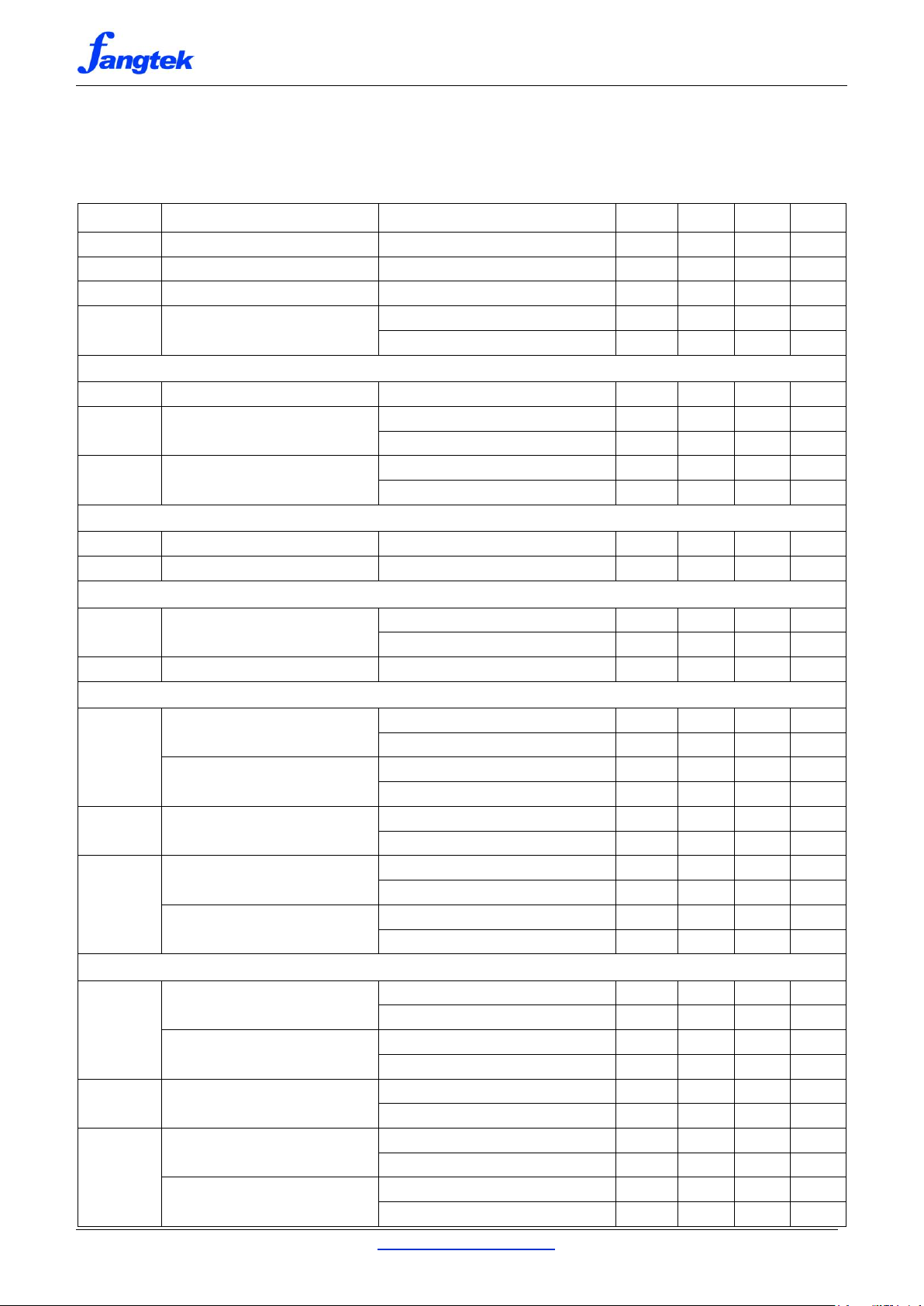
SYMBOL
PARAMETER
CONDITIONS
MIN
TYP
MAX
UNIT
TSTUP
Startup Time
80 ms
TSD
Shutdown Mode Settling Time
40 ms
fSW
PWM Output Carrier Frequency
400 kHz
ILIMIT
Over-Current Limit
SDRIVE=Low or High
2.6 A/Ch
SDRIVE=Unconnected
1.6 A/Ch
Automatic Level Control (ALC)
AMAX
Maximum ALC Attenuation
12 dB
TATTACK
ALC Attack Time
(VIN=0.24VRMS → 0.75VRMS)
ALC-1 Mode (ALC=Low)
6
ms
ALC-2 Mode (ALC=Unconnected)
48 ms
TRELEASE
ALC Release Time
(VIN=0.75VRMS → 0.24VRMS)
ALC-1 Mode (ALC=Low)
2.0 s
ALC-2 Mode (ALC=Unconnected)
1.0 s
Volume Fade-In & Fade-Out
TFADEIN
Fade-In Time
20 ms
TFADEOUT
Fade-Out Time
20 ms
Battery Tracking AGC
VKNEE
Knee Voltage
VKNEE=High
3.40 V
VKNEE=Unconnected
3.15 V
SATT
Output Attenuation Slope
@ VOPL/R, VONL/R
4
V/V
Class-D Audio Amplifier with Class-G Boost Regulator (SDRIVE=High, Soft Drive)
PO, MAX
Maximum Output Power
THD+N=10%
RL=4Ω 6.0
W/Ch
RL=8Ω 3.5
W/Ch
Maximum Output Power
THD+N=1%
RL=4Ω 4.8
W/Ch
RL=8Ω 2.8
W/Ch
PO, ALC
ALC Output Power
RL=4Ω, VIN=0.40VRMS
4.5
W/Ch
RL=8Ω, VIN=0.40VRMS
2.6
W/Ch
THD+N
Total Harmonic Distortion+Noise
(Non-ALC Mode)
RL=4Ω, Po=2W
0.08 %
RL=8Ω, Po=1W
0.08 %
Total Harmonic Distortion+Noise
(ALC Mode)
RL=4Ω, VIN=0.40VRMS
0.3 %
RL=8Ω, VIN=0.40VRMS
0.3 %
Class-D Audio Amplifier w/o Class-G Boost Regulator (SDRIVE=Unconnected, Soft Drive)
PO, MAX
Maximum Output Power
THD+N=10%
RL=4Ω 1.5
W/Ch
RL=8Ω
0.90
W/Ch
Maximum Output Power
THD+N=1%
RL=4Ω 1.2
W/Ch
RL=8Ω
0.70
W/Ch
PO, ALC
ALC Output Power
RL=4Ω, VIN=0.20VRMS
1.1
W/Ch
RL=8Ω, VIN=0.20VRMS
0.65
W/Ch
THD+N
Total Harmonic Distortion+Noise
(Non-ALC Mode)
RL=4Ω, Po=1W
0.08 %
RL=8Ω, Po=0.5W
0.08 %
Total Harmonic Distortion+Noise
(ALC Mode)
RL=4Ω, VIN=0.20VRMS
0.8 %
RL=8Ω, VIN=0.20VRMS
0.8 %
ELECTRICAL CHARACTERISTICS
(Note 5)
(Cont’d)
VBAT=3.6V, f=1kHz, Load=4Ω+33µH, L=3.3µH, CIN=0.22µF, RIN=15kΩ (Av=25dB), ALC=NC, VKNEE=Low,
SDRIVE=Low, CS=22µF, CPVOUT=22µF//220µF, CPVDDL/R=1µF, RVBAT=10Ω, CVBAT=1µF, RAVDD=10Ω,
CAVDD=1µF, CBVDD=0.1µF, both channels driven, TA=25°C, unless otherwise specified.
DEC, 2017 http://www.fangtek.com.cn 7
Page 8
ft2925
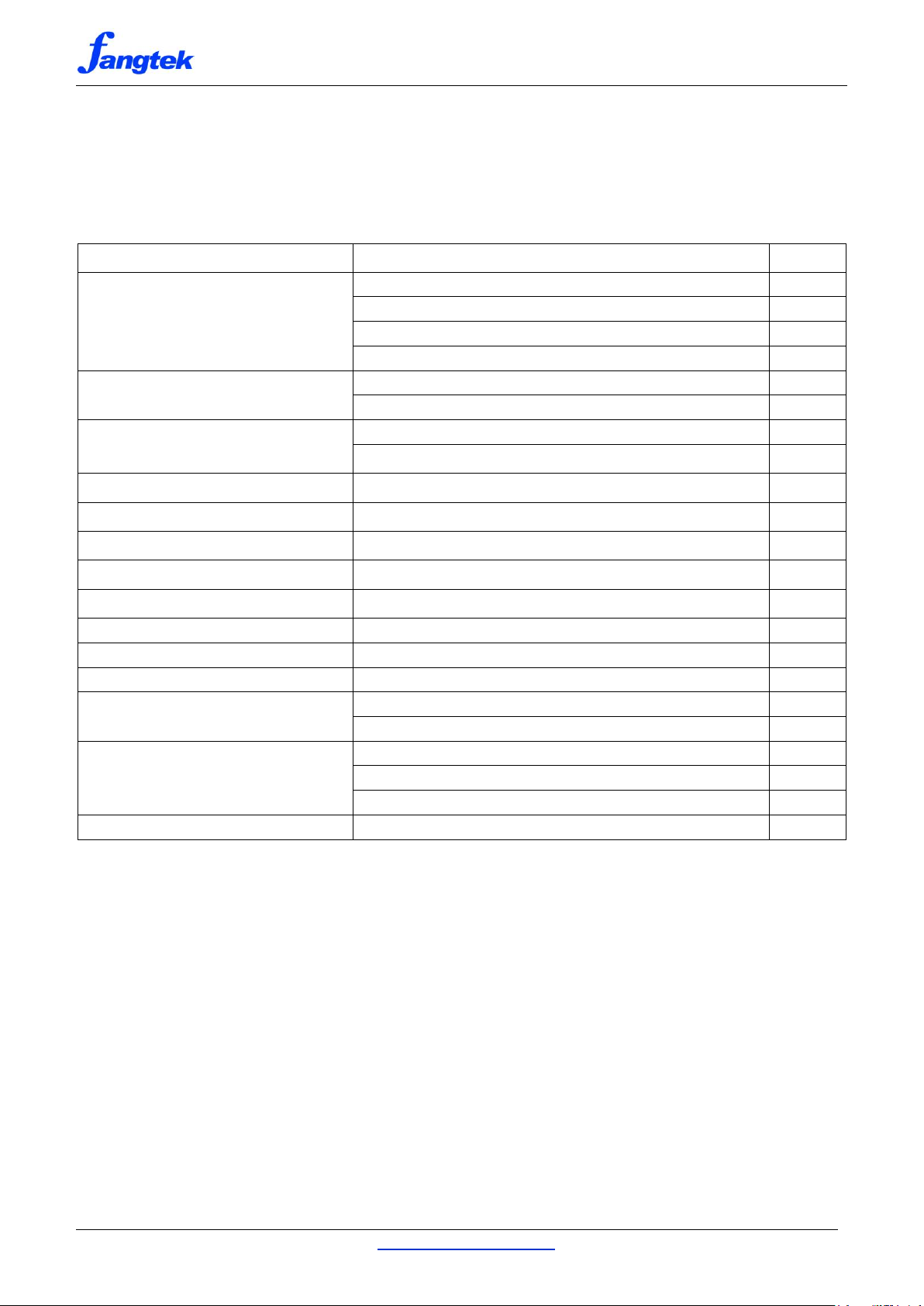
DESCRIPTION
CONDITIONS
FIGURE #
Output Power vs. Input Voltage
RL=4Ω+33µH, ALC-1 & ALC-2 & Non-ALC Modes
3
RL=8Ω+33µH, ALC-1 & ALC-2 & Non-ALC Modes
4
RL=4Ω+33µH, ALC-1 Mode, SDRIVE=High/Unconnected
5
RL=8Ω+33µH, ALC-1 Mode, SDRIVE=High/Unconnected
6
Output Power vs. Supply Voltage
VIN=0.40VRMS, RL=4Ω+33µH, VKNEE=High/Unconnected/Low
7
VIN=0.40VRMS, RL=8Ω+33µH, VKNEE=High/Unconnected/Low
8
Overall Efficiency vs. Output Power
RL=4Ω+33µH, Non-ALC Mode, SDRIVE= Low/High
9
RL=8Ω+33µH, Non-ALC Mode, SDRIVE=Low/High
10
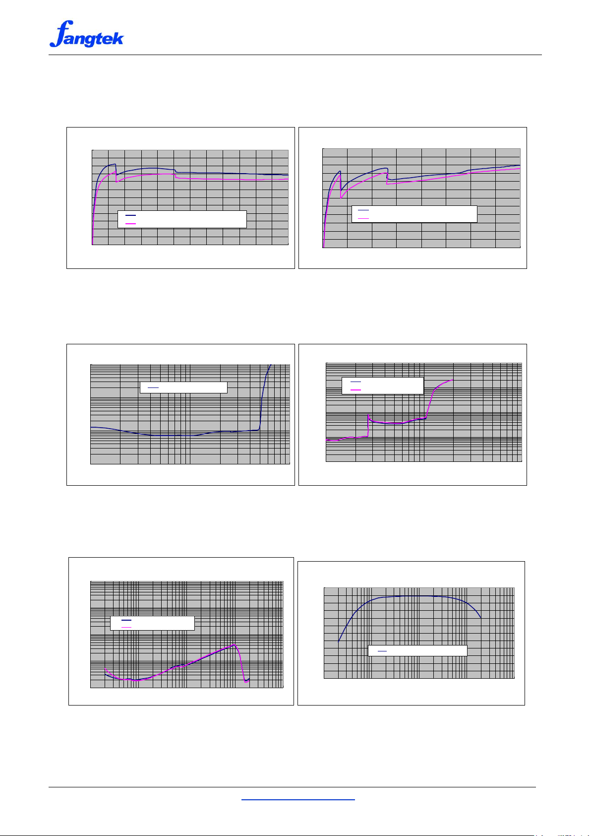
THD+N vs. Output Power
RL=4Ω+33µH, Non-ALC Mode
11
THD+N vs. Input Voltage
RL=4Ω+33µH, ALC-1 & ALC-2 Modes
12
THD+N vs. Input Frequency
Po=1W/3W, RL=4Ω+33µH, ALC-1 & ALC-2 Modes
13
Output Power vs. Input Frequency
VIN=0.20VRMS, RL=4Ω+33µH, Non-ALC Mode, f=20Hz ~ 20kHz
14
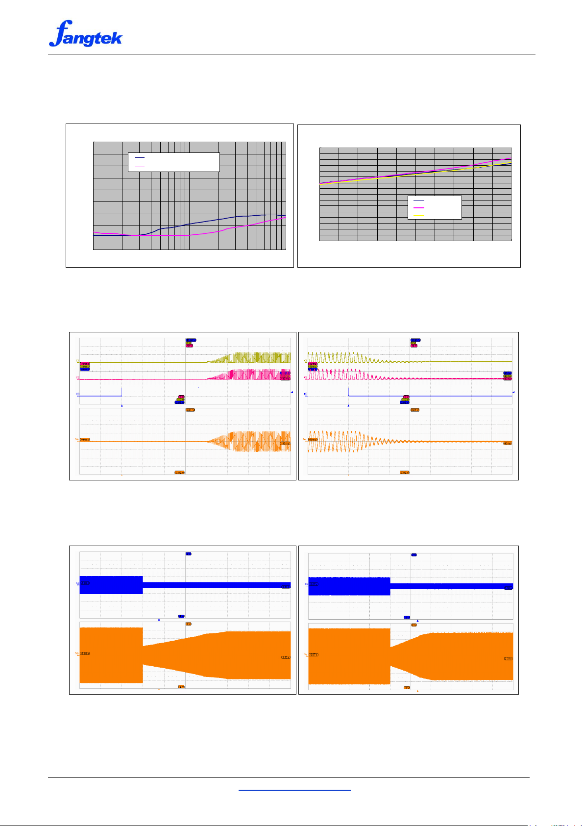
PSRR vs. Input Frequency
RL=4Ω+33µH, Inputs AC-Grounded
15
Quiescent Current vs. Supply Voltage
Input AC-Grounded, RL=No Load/4Ω+33µH/8Ω+33µH
16
Startup Output Waveforms
VIN=0.1VRMS
17
Shutdown Output Waveforms
VIN=0.1VRMS
18
ALC Release Time
VIN=0.75VRMS → 0.24VRMS, RL=4Ω+33µH, ALC-1 Mode
19
VIN=0.75VRMS → 0.24VRMS, RL=4Ω+33µH, ALC-2 Mode
20
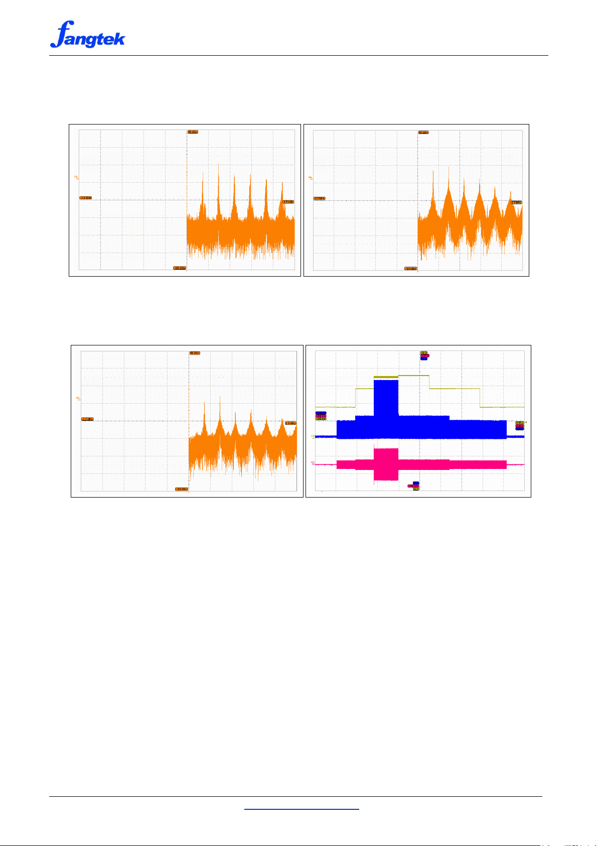
Broadband Output Spectrum
RL=4Ω+33µH, VIN=0.2VRMS, SDRIVE=Low
21
RL=4Ω+33µH, VIN=0.2VRMS, SDRIVE=High
22
RL=4Ω+33µH, VIN=0.2VRMS, SDRIVE=Unconnected
23
Mode Transitions of Boost Regulator
RL=4Ω+33µH, Non-ALC Mode
24
TYPICAL PERFORMANCE CHARACTERISTICS
(Note 5)
VBAT=3.6V, f=1kHz, Load=4Ω+33µH, L=3.3µH, CIN=0.22µF, RIN=15kΩ (Av=25dB), ALC=NC, VKNEE=Low,
SDRIVE=Low, CS=22µF, CPVOUT=22µF//220µF, CPVDDL/R=1µF, RVBAT=10Ω, CVBAT=1µF, RAVDD=10Ω,
CAVDD=1µF, CBVDD=0.1µF, both channels driven, TA=25°C, unless otherwise specified.
List of Typical Performance Characteristics
Note 5: All parameters are measured according to the conditions specified in Electrical and Typical Performance
Characteristics sections with the following notes, unless otherwise specified:
5.1. The two differential inputs are shorted for common-mode input voltage measurement. All other parameters are
taken with input resistors RIN=15Ω and input capacitors CIN=0.22µF, unless otherwise specified.
5.2. The boost regulator’s supply decoupling capacitor CS=22µF is placed close to the inductor.
5.3. The boost regulator’s inductor L=3.3µH and Schottky diode are placed tightly together and close to the LX pins.
5.4. The boost regulator’s output capacitors CPVOUT=22µF//220µF are placed close to the PVOUT pins.
5.5. The audio amplifiers’ supply decoupling capacitors CPVDDL/R=1µF are placed individually close to PVDDL/R pins.
5.6. An output inductor of 33µH is placed in series with the load resistor to emulate a speaker load for all AC and
dynamic parameters.
5.7. A 33kHz lowpass filter is added even if the analyzer has an internal lowpass filter. An RC lowpass filter (100Ω,
47nF) is used on each output for the data sheet graphs.
DEC, 2017 http://www.fangtek.com.cn 8
Page 9
ft2925
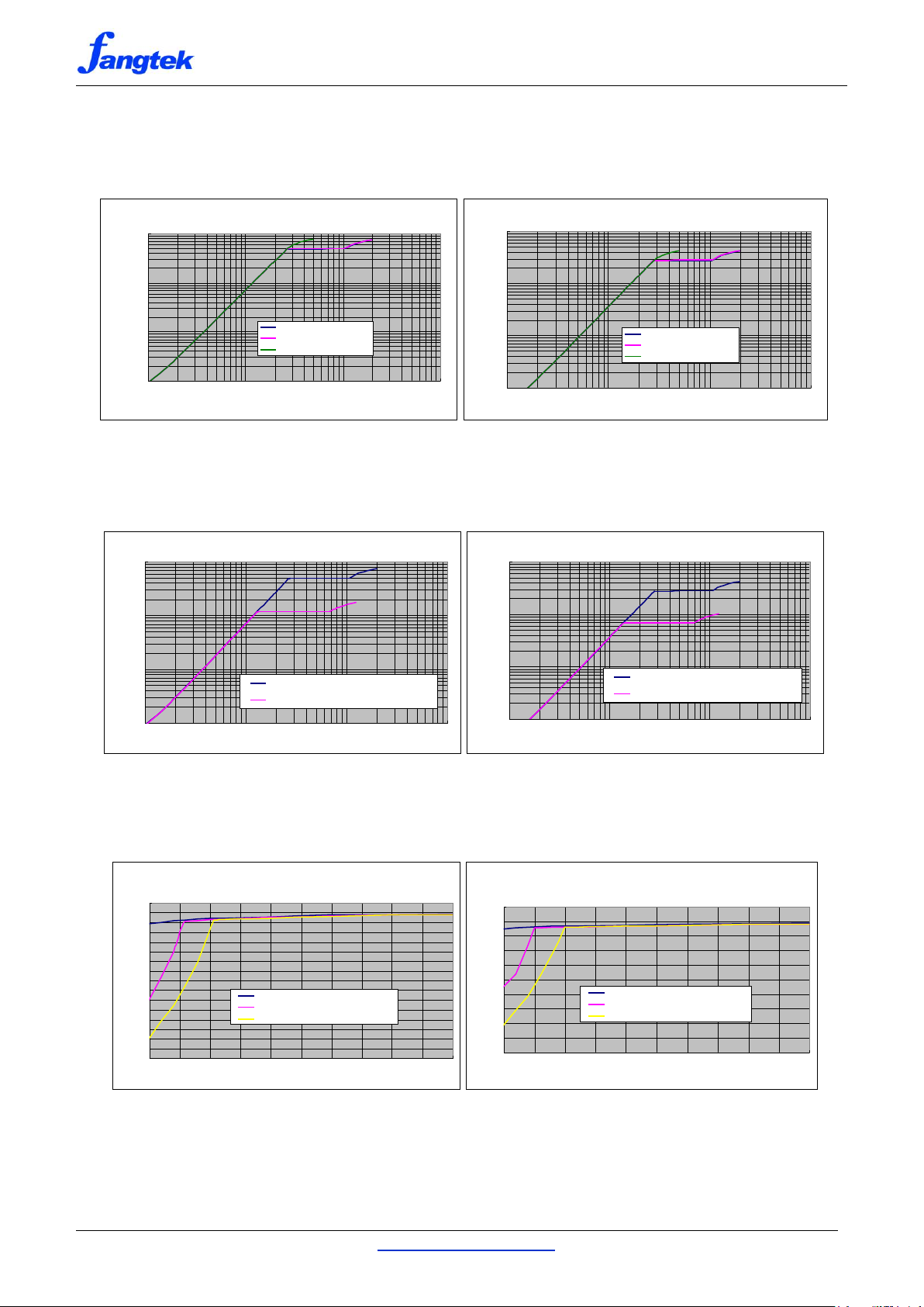
Output Power vs. Input Voltage
0.01
0.1
1
10
0.01 0.1 1 10
Input Voltage (Vrms)
Output Power (W)
ALC-1, RL=4Ω+33uH
ALC-2, RL=4Ω+33uH
Non-ALC, RL=4Ω+33uH
Output Power vs. Input Voltage
0.01
0.1
1
10
0.01 0.1 1 10
Input Voltage (Vrms)
Output Power (W)
ALC-1, RL=8Ω+33uH
ALC-2, RL=8Ω+33uH
Non-ALC, RL=8Ω+33uH
Output Power vs. Input Voltage
0.01
0.1
1
10
0.01 0.1 1 10
Input Voltage (Vrms)
Output Power (W)
ALC Mode, SDRIVE=High, RL=4Ω+33uH
ALC Mode, SDRIVE=NC, RL=4Ω+33uH
Output Power vs. Input Voltage
0.01
0.1
1
10
0.01 0.1 1 10
Input Voltage (Vrms)
Output Power (W)
ALC Mode, SDRIVE=High, RL=8Ω+33uH
ALC Mode, SDRIVE=NC, RL=8Ω+33uH
Output Power vs. Supply Voltage
2.0
2.4
2.8
3.2
3.6
4.0
4.4
4.8
5.2
3 3.5 4 4.5 5 5.5
Supply Voltage (V)
Output Power (W)
RL=4Ω+33uH, VKNEE Low
RL=4Ω+33uH, VKNEE Unconnected
RL=4Ω+33uH, VKNEE High
Output Power vs. Supply Voltage
1.0
1.4
1.8
2.2
2.6
3.0
3 3.5 4 4.5 5 5.5
Supply Voltage (V)
Output Power (W)
RL=8Ω+33uH, VKNEE Low
RL=8Ω+33uH, VKNEE Unconnected
RL=8Ω+33uH, VKNEE High
Figure 7: Output Power vs. Supply Voltage Figure 8: Output Power vs. Supply Voltage
Figure 3: Output Power vs. Input Voltage Figure 4: Output Power vs. Input Voltage
Figure 5: Output Power vs. Input Voltage Figure 6: Output Power vs. Input Voltage
TYPICAL PERFORMANCE CHARACTERISTICS (Cont’d)
DEC, 2017 http://www.fangtek.com.cn 9
Page 10
ft2925
Efficiency vs. Output Power
30
40
50
60
70
80
90
0 1 2 3 4 5 6
Output Power (W)
Efficient (%)
VDD=3.6V, RL=4Ω+33uH, SDRIVE Low
VDD=3.6V, RL=4Ω+33uH, SDRIVE High
Efficiency vs. Output Power
30
40
50
60
70
80
90
0 1 2 3 4
Output Power (W)
Efficient (%)
VDD=3.6V, RL=8Ω+33uH, SDRIVE Low
VDD=3.6V, RL=8Ω+33uH, SDRIVE High
THD+N vs. Output Power
0.01
0.1
1
10
0.1 1 10
Output Powre (W)
THD+N (%)
Non-ALC, RL=4Ω+33uH
THD+N vs. Input Voltage
0.01
0.1
1
10
100
0.1 1 10
Input Voltage (Vrms)
THD+N (%)
ALC-1, RL=4Ω+33uH
ALC-2, RL=4Ω+33uH
THD+N vs. Frequency
0.01
0.1
1
10
100
10 100 1000 10000 100000
Frequency (Hz)
THD+N (%)
RL=4Ω+33uH, Po=1W
RL=4Ω+33uH, Po=3W
Output Power vs. Frequency
0
0.5
1
1.5
2
2.5
3
10 100 1000 10000 100000
Frequency (Hz)
Output Power (W)
Vin=0.2Vrms, RL=4Ω+33uH
Figure 9: Overall Efficiency vs. Output Power Figure 10: Overall Efficiency vs. Output Power
Figure 13: THD+N vs. Input Frequency Figure 14: Output Power vs. Input Frequency
(with 33kHz Lowpass Filter)
Figure 11: THD+N vs. Output Power Figure 12: THD+N vs. Input Voltage
TYPICAL PERFORMANCE CHARACTERISTICS (Cont’d)
DEC, 2017 http://www.fangtek.com.cn 10
Page 11
ft2925
PSRR vs. Frequency
-90
-80
-70
-60
-50
-40
-30
-20
-10
0
100 1000 10000
Frequency (Hz)
PSRR (dB)
L-CH, Input AC-Grounded
R-CH, Input AC-Grounded
Quiescent Current vs. Supply Voltage
0
2
4
6
8
10
12
14
16
3 3.5 4 4.5 5 5.5
Supply Voltage (V)
Quiescent Current (mA)
No Load
RL=4Ω+33uH
RL=8Ω+33uH
X: 20ms/div
Y: 2V/div
X: 5ms/div
Y: 2V/div
VOP
VON
VOP-VON
VOP-VON
EN
EN
VOP
VON
VOP-VON (33kHz Lowpass Filter)
Figure 19: ALC-1 Release Time Figure 20: ALC-2 Release Time
VOP-VON (33kHz Lowpass Filter)
VIN=0.75VRMS ~ 0.24VRMS
X: 500ms/div
Y: 2V/div
X: 500ms/div
Y: 2V/div
VIN=0.75VRMS ~ 0.24VRMS
Figure 15: PSRR vs. Input Frequency Figure 16: Quiescent Current vs. Supply Voltage
Figure 17: Startup Output Waveforms Figure 18: Shutdown Output Waveforms
TYPICAL PERFORMANCE CHARACTERISTICS (Cont’d)
DEC, 2017 http://www.fangtek.com.cn 11
Page 12
ft2925
Figure 21: Wideband Output Spectrum Figure 22: Wideband Output Spectrum
Figure 23: Wideband Output Spectrum Figure 24: Mode Transitions of Boost Regulator
PVDD: 2V/div
Passthrough
Boost-1
Boost-2
Boost-1
Passthrough
VOP: 2V/div
VIN: 0.5V/div
X: 1s/div
SDRIVE=Low
SDRIVE=High
SDRIVE=Unconnected
TYPICAL PERFORMANCE CHARACTERISTICS (Cont’d)
DEC, 2017 http://www.fangtek.com.cn 12
Page 13

ft2925
APPLICATION INFORMATION
The ft2925 is a highly efficient 2x6W Class-G stereo audio power amplifier with automatic level control (ALC)
and battery tracking AGC. It integrates dual filterless Class-D audio amplifiers with a multi-level Class-G
synchronous boost regulator and operates with a range of supply voltages from 3V to 5.5V. When operating with
a 3.6V supply voltage, the ft2925 can deliver an output power of 6W per channel with 10% THD+N, or 4.8W per
channel with 1% THD+N, into a pair of 4Ω speakers.
In ft2925, the power supply rails of the audio amplifiers’ output stages are internally boosted and regulated by a
synchronous PWM switching regulator with two integrated power switches. The boost regulator employs
current-mode PWM control with proprietary multi-level Class-G operation to regulate the boosted output voltage.
The adaptive nature of the Class-G boost regulator, whose output voltage varies dynamically in response to the
voltage level of the audio outputs, improves overall power efficiency and extends battery life when playing music.
The higher output power and greater power efficiency resulted from the Class-G boost regulator make ft2925 an
ideal audio solution for battery-powered electronic devices.
The ft2925 features two modes of operation, i.e., ALC and Non-ALC, which can be selected via the ALC pin.
When the ALC pin is shorted to VBAT, the ft2925 operates in Non-ALC mode, where the audio amplifiers are
configured as conventional Class-D amplifiers without ALC. Conversely, when the ALC pin is unconnected or
shorted to GND, the ft2925 operates in ALC mode, where the audio outputs are constantly monitored and
safeguarded against the boosted supply voltage, preventing output clipping distortion, excessive power
dissipation, and speaker over-load. Once an over-level condition is detected, the ALC lowers the voltage gain of
both audio amplifiers together to eliminate output clipping while allowing for a maximally-allowed dynamic range
of the audio outputs. The ft2925 offers two ALC dynamic characteristics for two distinctive sound effects, which
are also selected via the ALC pin. In ALC mode, with a supply voltage at 3.6V, the ft2925 can deliver an ALC
output power of 4.5W per channel with 0.3% THD+N, into a pair of 4Ω speakers.
In conjunction with ALC, as the battery supply voltage drops below a prescribed value, the battery tracking AGC
lowers the voltage gain of both audio amplifiers to limit the peak audio outputs, preventing the collapse of battery
voltage.
Furthermore, the Class-D audio amplifiers in ft2925 feature filterless PWM modulators that substantially lower or
completely eliminate the requirement for external LC filters, reducing the number of external components, the
system board space, and the system cost. With filterless PWM modulators, the efficiency of the audio amplifiers
is also improved.
As specifically designed for portable applications, the ft2925 incorporates shutdown mode to minimize the power
consumption by holding the EN pin to ground. It also includes comprehensive protection features against various
operating faults such as over-current, short-circuit, over-temperature, or under-voltage for a safe and reliable
operation.
ADAPTIVE BOOST REGULATOR
To allow for higher audio loudness, a Class-G boost regulator is integrated in ft2925 to boost the power supply
rails (PVDDL/R) of the audio amplifiers’ output stages from VBAT to a higher voltage in response to the voltage
level of the audio outputs. For a proper operation, the power supply rails (PVDDL/R) must be externally shorted
to PVOUT, the voltage output of the boost regulator, via sufficiently wide metal lines on the system board.
The integrated boost regulator employs fixed-frequency, peak-current PWM scheme with current mode control.
The PWM switching frequency is internally set at 800kHz, which allows using smaller inductance and output
capacitance for stability and results in a higher PWM control loop bandwidth. Furthermore, the adaptive boost
regulator features proprietary multi-level operation. As either one of the audio outputs is higher than the first
prescribed value for an extended period, the ft2925 enters into Boost-1 mode, where the boost regulator is
activated to boost and regulate PVOUT at an intermediate value. As either one of the audio outputs grows higher
than the second prescribed value for an extended period, the ft2925 enters into Boost-2 mode, where PVOUT is
further boosted and regulated at its final value, at 7.2V, typically.
DEC, 2017 http://www.fangtek.com.cn 13
Page 14

ft2925
Conversely, when both audio outputs are reduced to be lower than the second prescribed value for an extended
period, the boost regulator returns back to Boost-1 mode. If both audio outputs are further reduced to be lower
than the first prescribed value for an extended period, the ft2925 is forced into Passthrough mode, where the
boost regulator is de-biased. In Passthrough mode, the audio amplifiers’ output stages are powered directly from
the supply input voltage, through the inductor and on-chip rectification power switch. Thus, in Passthrough mode,
PVOUT is equal to the supply input voltage minus the voltage drop across the rectification power switch.
The adaptive nature of the Class-G boost regulator in ft2925, where PVOUT varies dynamically in response to
the voltage level of the audio outputs, can greatly improve overall power efficiency and extend battery life when
playing music. The higher output power and greater efficiency make the ft2925 an ideal audio solution for
battery-powered electronic devices.
DESIGN GUIDELINES OF BOOST REGULATOR
Selection of Boost Regulator Inductor
The selection of the inductor is the most important consideration in the design of power switching regulators
since it affects the boost regulator’s steady-state operation as well as dynamic response and loop stability.
Three important inductor specifications are to be considered: Inductor value, DC resistance (DCR), and
Saturation current. Note that inductor values may have tolerance up to +20% with zero-current bias. Also,
when the inductor current approaches its saturation limit, the effective inductance can fall to a fraction of its
zero-current value. For typical applications, the recommended inductor peak (saturation) current ratings for
speak loads of 4Ω and 8Ω are higher than 8A and 5A, respectively.
In general, a larger inductance value produces less inductor current ripple, which in turn results in lower
inductor peak current, higher output current, lower EMI, and higher efficiency. On the other hand, a smaller
inductance value, with a physically small size, results in an improved transient response with higher inductor
peak current and potentially worse EMI and lower efficiency. An inductor in the range from 1.5µH to 3.3µH
suffices for most applications of ft2925. Do not use any inductance higher than 4.7µH as it requires a larger
output capacitance for stability of the PWM control loop, which in turn slows the boost regulator’s response
to load transients to a large extent with little improvements on the output current capability or efficiency.
Select an inductor with DCR less than 30mΩ for higher overall efficiency (from the power supply to the
speaker load).
Selection of Boost Regulator Output Capacitor
The output capacitor of the boost regulator is required to keep the output voltage ripple small and ensure the
stability of the PWM control loop. The output capacitor must have low equivalent-series-resistance (ESR) at
the PWM switching frequency, so ceramic capacitors are the best choice. Make sure that the output
capacitors maintain their capacitances over the specified range of DC bias and operating temperature. A
22µF low-ESR ceramic capacitor suffices for most applications with speaker load impedances of 8Ω. For
applications where the speaker load impedances are 4Ω or less, use a pair of 22µF low-ESR ceramic
capacitors.
A bulk output capacitor (either electrolytic or tantalum) is typically added to facilitate higher voltage margin
for higher audio power at low frequencies. However, be cautious using any bulk output capacitance higher
than 220µF as it might adversely slow the boost regulator’s response to load transients to some extent
affecting audio dynamics when playing music.
Also, add a small, good quality, low-ESR ceramic capacitor of 0.1µF in close proximity to the PVOUT pins for
high-frequency filtering.
The boost regulator’s output, PVOUT, must be externally connected to the power supply rails of the audio
amplifiers’ output stages, PVDDL/R, on the system board with wide and short metal traces.
Selection of Boost Regulator Schottky Diode
A rectification power switch is integrated in the synchronous boost regulator of ft2925, thus no external
DEC, 2017 http://www.fangtek.com.cn 14
Page 15

ft2925
LX
PGNDB
CLX
RLX
Schottky diode is necessary for applications with speaker load impedances of 8Ω. However, for applications
where speaker load resistances are 4Ω or less, it is required to add an auxiliary Schottky diode across LX
and PVOUT pins to improve maximum output power and overall power efficiency. The added Schottky diode
must be rated for a current no less than 5A and a reverse breakdown voltage no less than 15V.
Selection of Boost Regulator Input Capacitor
In practice, supply input capacitors are required for boost regulators. The supply input capacitor acts as a
charge reservoir for the inductor current, providing energy faster than the system power supply, mitigating
current surges or voltage droops of the supply voltage.
At least 10µF of input capacitance is required for supply decoupling for ft2925. The rated voltage of the input
capacitor must be higher than the supply input voltage with sufficient tolerance to limit the effects of dc bias.
For most applications where the power supply is reasonably designed, a low-ESR ceramic capacitor of 22µF,
16V with 10mΩ ESR is sufficient for ft2925. Also, add a small, good quality, low-ESR ceramic capacitor of
0.1µF in close proximity to the inductor for high-frequency supply decoupling.
For applications where additional input capacitance is required to meet the requirement of the input current
ripple or transient response, place an electrolytic or tantalum bulk capacitor between 47µF and 100µF in
close proximity to ft2925. The bulk capacitor acts as a charge reservoir for the inductor current, providing
energy faster than the system power supply, mitigating current surges and/or voltage droops of the supply
voltage.
Boost Regulator Snubber Circuit
It is not uncommon for a boost regulator to observe voltage oscillations in a frequency range of 100 ~
200MHz at the switch node LX due to parasitic inductances and capacitances on its high-current path. If the
amplitude of the voltage ringing is above the absolute maximum rating of the LX pin, the on-chip power
switches can be damaged permanently.
For applications where excessive voltage spikes or oscillations are observed due to severe restrictions on
the board layout, it may become necessary to add a snubber circuit from the switch node LX to the power
ground PGNDB to lower voltage spikes and eliminate voltage oscillations at the switch node. A snubber
circuit, a small resistor in series with a small capacitor, is an energy-absorbing circuit to provide an
alternative path to ground for the current flowing through the parasitic inductances. In practice, the snubber
circuit is added to lower EMI emissions as well as enhance the operational reliability of the boost regulator.
Figure 25 shows an RC snubber circuit with suggested values of RLX=1Ω and CLX=2.2 ~ 10nF. Note that the
design of the RC snubber circuit is specific to each application and board layout, thus the parasitic
inductances and capacitances must be taken into consideration to reach proper values of RLX and CLX.
Evaluate and ensure that the voltage spikes at LX are within the absolute maximum rating of LX on the
actual system board. Pay close attention to the layout of the snubber circuit to be tight and in close proximity
to LX and PGNDB pins.
Note that the RC snubber circuit will adversely affect the overall efficiency of the boost regulator by a few
percent, which is a function of the CLX value.
Figure 25: Boost Regulator Snubber Circuit
DEC, 2017 http://www.fangtek.com.cn 15
Page 16
ft2925
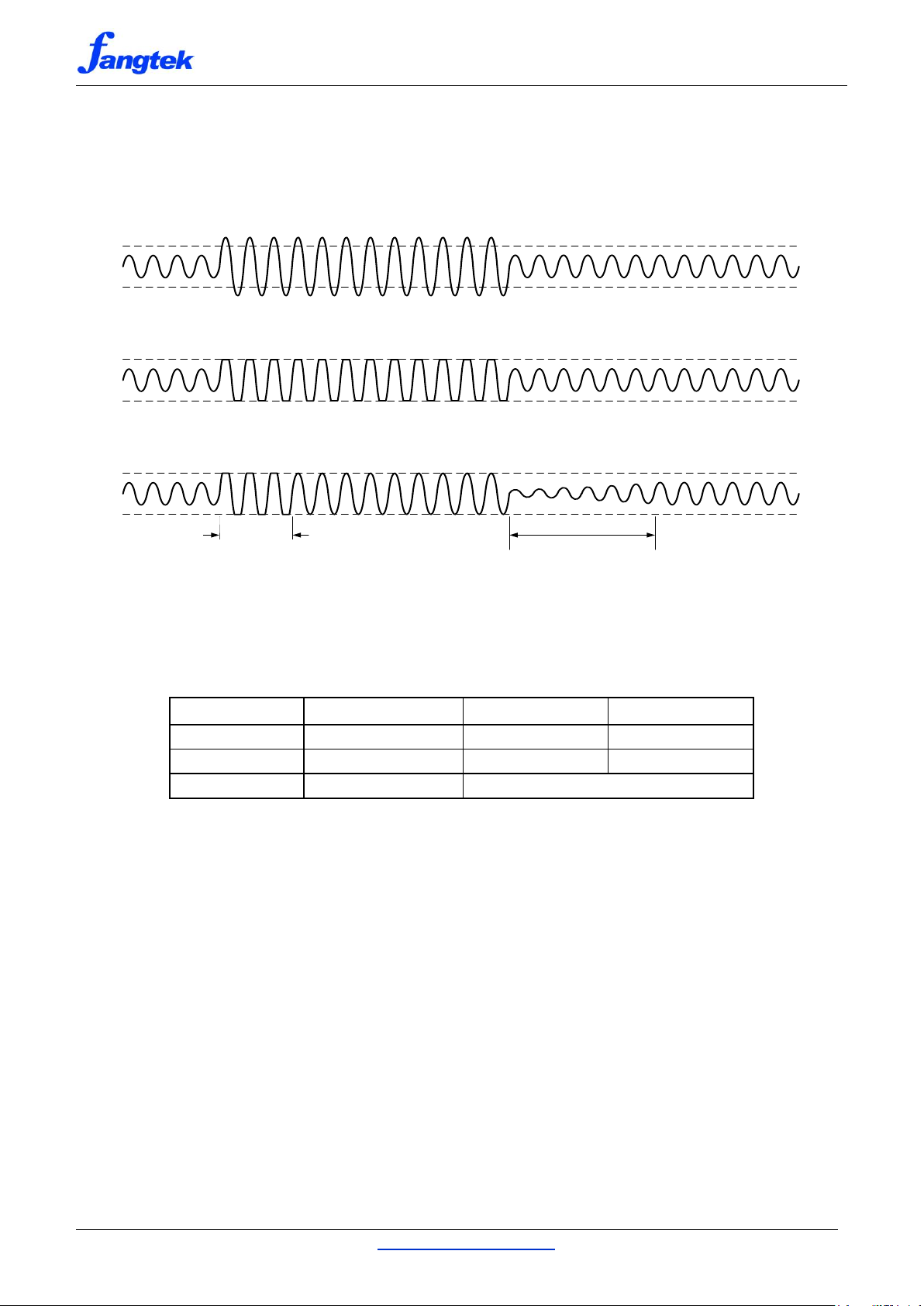
Attack Time Release Time
Output Signal when Supply Voltage is Sufficiently Large
Output Signal in ALC Off Mode
Output Signal in ALC On Mode
ALC
Mode of Operation
Attack Time (ms)
Release Time (s)
Low
ALC-1
6
2.0
Unconnected
ALC-2
48
1.0
High
Non-ALC
N/A
AUTOMATIC LEVEL CONTROL (ALC)
The automatic level control (ALC) is to maintain the audio outputs for a maximum voltage swing without clipping
when excessive inputs that may cause clipping distortion are applied. With ALC, the ft2925 lowers the gain of the
audio amplifiers to an appropriate value such that output clipping is substantially eliminated.
Figure 28: Automatic Level Control Diagram
The attack time and release time of the ALC are shown in Table 3. The attack time is defined as the time interval
required for the gain to fall to its steady-state gain less 3dB approximately, assumed that a sufficiently large input
signal is applied. The release time is the time interval required for the amplifier to exit out of the present mode of
operation.
Table 3: Attack Time & Release Time
ALC MODE CONTROL
The ft2925 can be configured in ALC or Non-ALC mode via the ALC pin, as described in Table 3. When the ALC
pin is shorted to VBAT, the ft2925 operates in Non-ALC mode. The Non-ALC operation is typically chosen for
applications where maximum audio loudness is much desired and output clipping distortion can be properly
controlled and largely eliminated at the audio sources. Conversely, when the ALC pin is left unconnected or
shorted to GND, the ft2925 operates in ALC mode with two sets of dynamic characteristics. For most
applications, the ALC mode of operation is much preferred for its capability to substantially eliminate output
clipping distortion, excessive power dissipation, and speaker over-load.
Two sets of ALC dynamic characteristics can be selected for specific sound effects, as described in Table 3. The
ALC-1 mode, where the ALC pin is shorted to GND, tends to play music in a mellower manner with negligible
amount of clipping distortion and lower average output power (loudness). On the other hand, the ALC-2 mode,
where the ALC pin is left unconnected, tends to play music in a more dynamic manner with higher average
output power and some extent of clipping distortion.
DEC, 2017 http://www.fangtek.com.cn 16
Page 17
ft2925
20+R
600
=A
IN
V
RIN (kΩ)
0
3.9
6.8
10
14
18
22
27
33
39
47
56
AV (V/V)
30
25
22.4
20
17.6
15.8
14.3
12.8
11.3
10 9 8
AV (dB)
29.5
28
27
26
25
24
23
22
21
20
19
18
VIN, MAX (VRMS)
RIN (kΩ)
AV (V/V)
AV (dB)
0.30
3.9
25
28
0.50
15
17
25
0.70
27
13
22
1.0
47 9 19
MAX,IN
V
V
PVDD×α
=A
CINR1
INPL
INNLINNL
INNR
RINL1
INPL
INNR
RINR1
CINL2
RINR2
INNR
INNL
INPL
RINL2
INNL
RINR2
RINL2
CINL2
RINR1
INPR
CINR2
CINL1 RINL1
INNR
INPR
CINR1
CINL1
INPR
CINR2
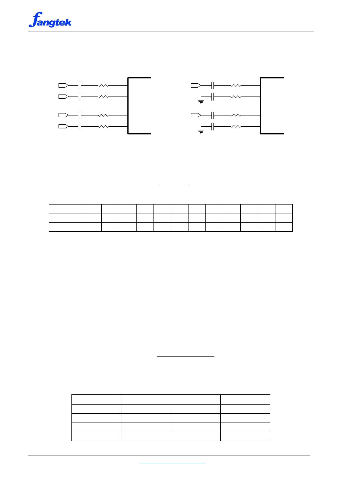
VOLTAGE GAIN SETTING
The voltage gain of the audio amplifiers can be externally adjusted by inserting additional input resistors in series
with input capacitors, as depicted in Figure 26 and 27. In typical applications, it is required that CIN = CINL1 = CINL2
= CINR1 = CINR2 and RIN = RINL1 = RINL2 = RINR1 = RINR2.
Figure 26: Gain Setting (Differential Inputs) Figure 27: Gain Setting (Single-Ended Inputs)
The value of RIN (in kΩ) for a given voltage gain can be calculated by Equation 1. Table 1 shows suitable resistor
values of RIN that can be used for various voltage gains, where AV is the voltage gain of the audio amplifiers.
(1)
Table 1: External Input Resistors Required for Various Voltage Gains
The choice of the voltage gain will strongly influence the loudness and quality of audio sounds. In general, the
higher the voltage gain is, the louder the sound is perceived. However an excessive voltage gain may cause the
audio outputs to be noticeably compressed or clipped for high-level (loud) audio sounds. On the other hand, an
unusually low gain may cause relatively low-level (quite) sounds soft or inaudible. Thus it is crucial to choose a
proper voltage gain for well balanced audio quality.
The voltage gain is chosen based upon various system-level considerations including the boosted supply
voltage, dynamic range of the audio source, output power rating, and desired sound effect. The voltage gain can
be simply expressed in Equation 2. In the equation, VIN, MAX (in VRMS) is the maximum input level from the audio
source, PVDD (in volts) is the boosted supply voltage, and α is the design parameter, which ranges from 0.65 to
2.5. The higher α is, the higher the average output power (louder) is, with some degree of compression for
high-level audio sounds.
(2)
As an example, Table 2 shows the voltage gain for various audio input levels with α at about 1.2. In the table, RIN
is the external input resistor in series with the input capacitor.
Table 2: Typical Voltage Gain Settings for Various Audio Input Levels
DEC, 2017 http://www.fangtek.com.cn 17
Page 18
ft2925
SDRIVE
Boost Regulator
Driver Mode
Description
Low
Enable
High Efficiency Drive
High Efficiency, High Power
Unconnected
Disable
Soft Drive
Lowest EMI, Low Power Operation
High
Enable
Soft Drive
Low EMI, Medium Power Operation
VKNEE
Knee Voltage (V)
Low
Battery Tracking AGC Disabled
Unconnected
3.15
High
3.40
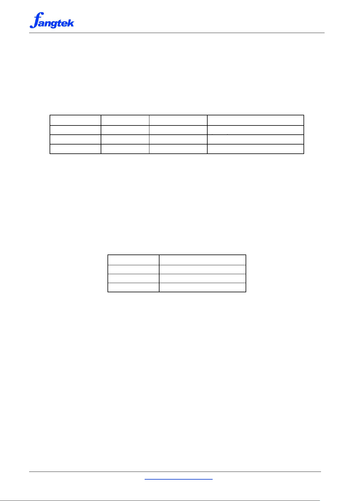
SOFT DRIVE MODE
To facilitate low EMI operation to minimize FM interference, the ft2925 features proprietary edge-rate-control
gate drivers for both Class-D audio amplifiers and the Class-G boost regulator. In the soft drive mode, the EMI
emissions will be largely reduced at the expense of lower power efficiency, however, much higher than the
traditional Class-AB audio amplifiers. Furthermore, to further reduce EMI emissions, the boost regulator can be
disabled at the expense of much lower maximum output power due to the limited power supply (the battery
voltage) available to the audio amplifiers. Three operating modes are available in ft2925 and can be selected via
the SDRIVE pin, as described in Table 4.
Table 4: Soft Drive Mode Control
BATTERY TRACKING AGC
The ft2925 features battery tracking AGC to limit the peak audio outputs as the battery voltage droops. Although
it will affect audio output loudness on low battery voltages, the battery tracking AGC limits high battery current at
the end-of-charge battery voltage and prevents the battery voltage from collapsing, which might cause a reset of
the system. The battery tracking AGC keeps the peak audio outputs below a limiting value that is a function of
the battery supply voltage. The peak output voltage is maintained at PVDD for battery voltages down to the knee
voltage and reduced linearly at a rate of 4V/V for lower battery voltages. The knee voltage of the battery tracking
AGC can be selected via the VKNEE pin, as described in Table 5. Note that the battery tracking AGC can be
enabled only when the ALC function is enabled where the ALC pin is pulled low or left unconnected.
Table 5: Battery Tracking AGC Control
The operation of the battery tracking AGC can be highly influenced by the electrical characteristics of the battery
used with ft2925. Place a small decoupling resistor of 10Ω between the battery supply voltage and the VBAT pin
in conjunction with a decoupling capacitor of 1µF, mitigating the detrimental effect of high battery current ripples
on the detection of battery voltage.
SHUTDOWN AND STARTUP
The ft2925 employs the EN pin to minimize power consumption while it is not in use. When the EN pin is pulled
to ground, the ft2925 is forced into shutdown mode, where all the analog circuitry is de-biased and the supply
current is reduced to be less than 1µA, and the differential outputs are shorted to ground through an internal
resistor (3kΩ) individually. Once in shutdown mode, the EN pin must remains low for at least 40ms (TSD), the
shutdown settling time, before it can be brought high again. When the EN pin is asserted high, the device exits
out of shutdown mode and enters into normal operation after the startup time (TSTUP) of 80ms.
Note that an internal pulldown resistor of 300kΩ is included onto the EN pin. Thus, shutdown mode is the state
when the power supply is first applied to the device. Whenever possible, it is recommended to assert EN high to
exit the device out of shutdown mode only after the device is properly started up. Also, place the amplifier in
shutdown mode prior to removing the power supply voltage for the best power-off pop performance.
DEC, 2017 http://www.fangtek.com.cn 18
Page 19

ft2925
Fade In
Time
Fade Out
Time
VOLUME FADE-IN & FADE-OUT
The volume fade-in/out function is activated whenever the EN state is toggled. It can reduce intermittent sound
considerably and eliminate uncomfortable hearing experience.
Figure 29: Fade-In Output Waveform Figure 30: Fade-Out Output Waveform
CLICK-AND-POP SUPPRESSION
The ft2925 features comprehensive click-and-pop suppression. During startup, the click-and-pop suppression
circuitry reduces any audible transients internal to the device. When entering into shutdown, the differential audio
outputs ramp down to ground simultaneously.
PSRR ENHANCEMENT
Without a dedicated pin for the common-mode voltage bias, the ft2925 achieves a PSRR, 70dB at 1kHz.
PROTECTION MODES
To ensure a safe operation, the ft2925 incorporates various protection modes against operating faults, including
Under-voltage Lockout (UVLO), Over-Current Protection (OCP), and Over-Temperature Shutdown (OTSD).
Under-Voltage Lockout (UVLO)
The ft2925 incorporates a circuitry to detect a low supply voltage for a safe and reliable operation. When the
supply voltage is first applied, the ft2925 will remain inactive until the supply voltage exceeds 2.3V (VUVLU).
When the supply voltage is removed and drops below 2.0V (VUVLD), the ft2925 enters into shutdown mode
immediately.
Over-Temperature Shutdown (OTSD)
When the die temperature exceeds a preset threshold (160C), the device enters into over-temperature
shutdown mode, where the audio outputs are pulled to ground through their individual on-chip resistors
(3kΩ). The device will resume normal operation once the die temperature returns to a lower temperature,
which is about 20C lower than the threshold.
Over-Current Protection (OCP)
During operation, the output of Class-D amplifier constantly monitors for any over-current or short-circuit
conditions. When an over-current condition between two differential outputs, differential output to PVDDL/R
or PGND is detected, the output stage of the amplifier is immediately forced into high impedance state.
Once the fault condition persists over a prescribed period, the ft2925 then enters into shutdown mode and
remains in this mode for about 8ms. When shutdown mode times out, the ft2925 will initiate another startup
sequence and then check if the over-current condition has been removed. If the fault condition is still
present, the ft2925 will repeat itself for the process of a startup followed by detection, qualification, and
shutdown. It is the so-called hiccup mode of operation. Once the fault condition is removed, the ft2925
automatically resumes normal operation.
Although the output stages of the Class-D audio amplifiers can withstand a short between VOPL/R
and VONL/R, do not connect any audio outputs directly to GND, PVOUT, or PVDDL/R as this might
damage the device permanently.
DEC, 2017 http://www.fangtek.com.cn 19
Page 20
ft2925
FB1
VON
Ferrite Chip Bead
C2
FB2
Ferrite Chip Bead
C1
SPEAKER
VOP
CLASS-D AUDIO AMPLIFIER
The Class-D audio amplifiers in the ft2925 operate in much the same way as traditional Class-D amplifiers and
similarly offer much higher power efficiency than Class-AB amplifiers. The high efficiency of Class-D operation is
achieved by the switching operation of the output stage of the amplifier. The power loss associated with the
output stage is limited to the conduction and switching loss of the power switches, which are much less than the
power loss associated with a linear output stage in Class-AB amplifiers.
Fully Differential Amplifier
The ft2925 includes a pair of fully differential amplifiers with differential inputs and outputs. The fully differential
amplifiers ensure that the differential output voltages are equal to the differential input voltages times the
amplifier gain. Although the ft2925 supports for a single-ended input, differential inputs are much preferred for
applications where the environment can be noisy in order to ensure maximum SNR.
Low-EMI Filterless Output Stage
Traditional Class-D audio amplifiers require for the use of external LC filters, or shielding, to meet EN55022B
electromagnetic-interference (EMI) regulation standards. The ft2925 applies an edge-rate control circuitry to
reduce EMI emissions, while maintaining high power efficiency.
Filterless Design
Traditional Class D amplifiers require an output filter to recover the audio signal from the amplifier’s output. The
filter adds cost, increases the solution size of the amplifier, and can adversely affect efficiency and THD
performance. The traditional PWM scheme uses large differential output swings (twice of the supply voltage) and
causes large ripple currents. Any parasitic resistance in the filter components results in loss of power and lowers
the efficiency.
The ft2925 does not require an output filter. The device relies on the inherent inductance of the speaker coil and
the natural filtering of both the speaker and the human ear to recover the audio component of the square-wave
output. By eliminating the output filter, a smaller, less costly, and more efficient solution can be accomplished.
Because the frequency of the audio outputs from ft2925 is well beyond the bandwidth of most speakers, voice
coil movement due to the square-wave frequency is very small. Although this movement is small, a speaker not
designed to handle the additional power can be damaged. For optimum performance, use speakers with series
inductances greater than 10uH. Typical 4Ω speakers exhibit series inductances in the range from 10µH to 47uH.
EMI Reduction
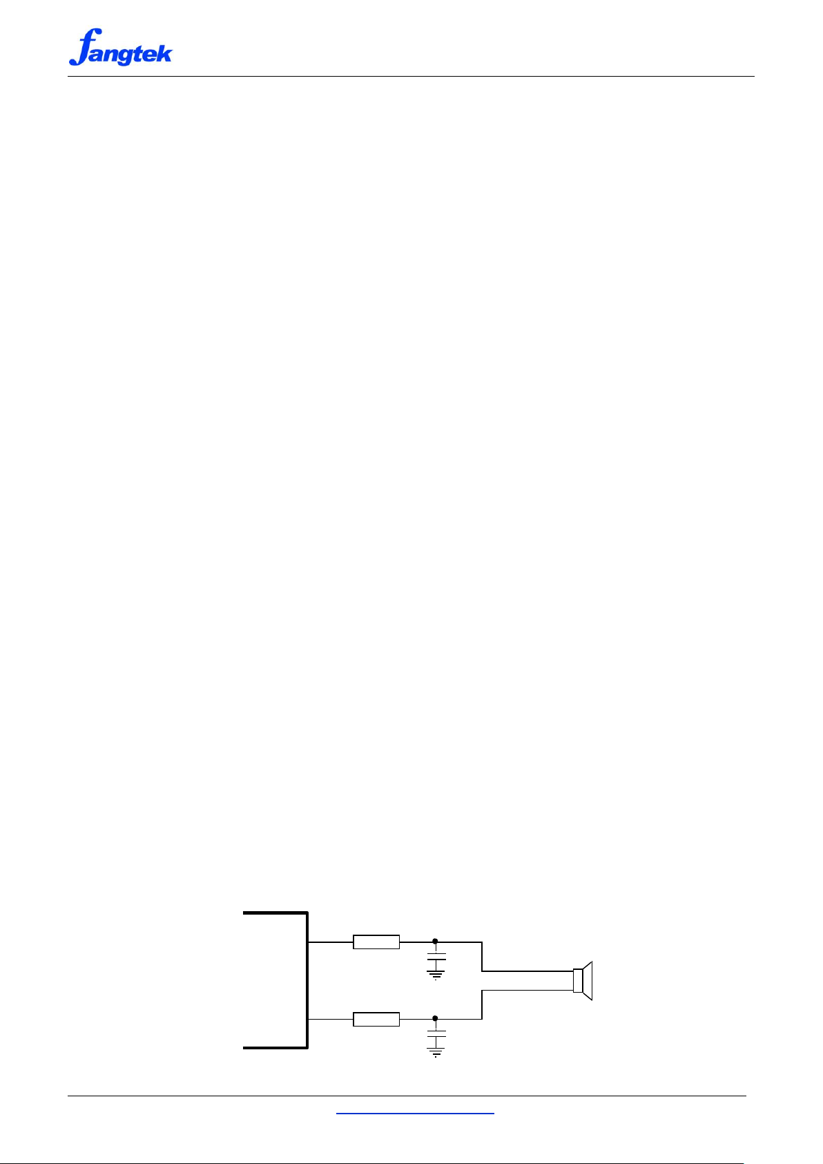
The ft2925 does not require an LC output filter for the connections from the amplifier to the speaker. However,
additional EMI suppression can be made by use of a ferrite bead filter comprising a ferrite bead and a capacitor,
as shown in Figure 31. Choose a ferrite bead with low DC resistance (DCR) and high impedance (100Ω ~ 330Ω)
at high frequencies (>100MHz). The current flowing through the ferrite bead must be also taken into
consideration. The effectiveness of ferrites can be greatly aggravated at much lower than the rated current
values. Choose a ferrite bead with a rated current no less than 2A for an 8Ω load and 3A for a 4Ω load. The
capacitor value varies based on the ferrite bead chosen and the actual speaker lead length. Choose a capacitor
less than 1nF based on EMI performance. Place each ferrite bead filter tightly together and individually close to
VOPL/R and VONL/R pins respectively.
Figure 31: Ferrite Bead Filter to Reduce EMI
DEC, 2017 http://www.fangtek.com.cn 20
Page 21
ft2925
C
SPEAKER
VOP
VON
R
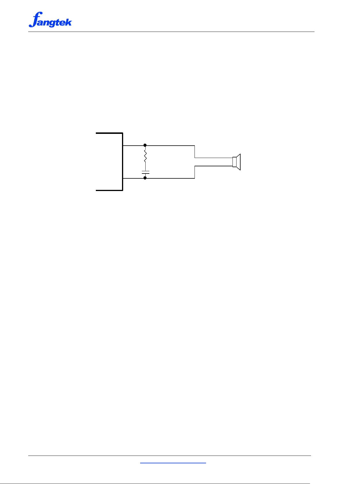
Class-D Output Snubber Circuit
For applications where speaker load resistances are 4Ω or less, it may become necessary to add a snubber
circuit across the two output pins, VOPL/R and VONL/R, to prevent the device from accelerated deterioration or
abrupt destruction due to excessive inductive flybacks that are induced on fast output switching or by an
over-current or short-circuit condition. The snubber circuit can further lower EMI emission of Class-D outputs.
Figure 32 shows a simple RC snubber circuit with suggested values of R=4.7Ω in series with C=4.7nF. Note that
the design of the RC snubber circuit is specific to each application and must take into account the parasitic
reactance of the system board to reach proper values of R and C. Evaluate and ensure that the voltage spikes
(overshoots and undershoots) at VOPL/R and VONL/R on the actual system board are within their absolute
maximum ratings. Pay close attention to the layout of the RC snubber circuit to be tight and individually close to
VOPL/R and VONL/R pins, respectively.
Figure 32: Class-D Output RC Snubber Circuit
Input Capacitor (CIN)
DC decoupling capacitors for audio inputs (INPL/R and INNL/R) are recommended. The input audio DC
decoupling capacitors will remove the DC bias from audio inputs. The input capacitor CIN and the total input
resistance (RIN + 20kΩ) form a highpass filter with the corner frequency, fC, determined by Equation 3.
fC = 1 / [2 x π x (RIN +20kΩ) x CIN] (3)
where RIN=RINL1=RINL2=RINR1=RINR2 and CIN=CINL1=CINL2=CINR1=CINR2
RIN is the external input resistance for a specific voltage gain. Note that the variation of the actual input
resistance will affect the voltage gain proportionally. Thus choose RIN with a tolerance of 2% or better.
Choose CIN such that fC is well below the lowest frequency of interest. Setting it too high affects the amplifiers’
low-frequency response. Consider an example where the specification calls for AV=25dB and a flat frequency
response down to 20Hz. In this example, RIN=15kΩ and CIN is calculated to be about 0.23µF; thus any
capacitance between 0.22µF and 0.47µF can be chosen for CIN.
Note that any mismatch in resistance and capacitance between two audio inputs will cause a mismatch in the
corner frequencies. Severe mismatch may also cause turn-on pop noise, PSRR, CMRR performance. Choose
both resistors and capacitors with a tolerance of ±2% or better.
Furthermore, the type of the input capacitor is crucial to audio quality. For best audio quality, use capacitors
whose dielectrics have low voltage coefficients, such as tantalum or aluminum electrolytic. Capacitors with high
voltage coefficients, such as ceramics, may result in increased distortion at low frequencies.
Supply Decoupling Capacitors (CVBAT, CPVDDL/R, CAVDD, CBVDD)
Sufficient decoupling of the power supplies is crucial for audio amplifiers to ensure high efficiency, low distortion,
and low EMI. Place a 1µF low-ESR ceramic capacitor (CVBAT) in close proximity to the VBAT pin. Furthermore,
add a small decoupling resistor (RVBAT) of 10Ω between the system power supply and the VBAT pin, minimizing
the detrimental effect of high battery current ripples on the detection of battery voltage.
Place a 1µF low-ESR ceramic capacitor (CPVDDL/R) individually close to each PVDDL/R pin.
Place a 1µF low-ESR ceramic capacitor CAVDD close to the AVDD pin. This capacitor type and placement of
CAVDD help minimize higher frequency transients, spikes, or digital hash on the supply line. Furthermore, add a
DEC, 2017 http://www.fangtek.com.cn 21
Page 22

ft2925
small decoupling resistor (RAVDD) of 10Ω between AVDD and PVOUT pins, preventing high frequency transients
of PVOUT from interfering with on-chip linear amplifiers.
Place a 0.1µF low-ESR ceramic capacitor CBVDD close to the BVDD pin for high-frequency filtering.
PRINTED CIRCUIT BOARD (PCB) LAYOUT GUIDELINES
Ground Plane - It is required to use a solid metal plane with sufficiently wide area as a central ground connection
(GND) for ft2925. All ground pins (AGND, PGND, and PGNDB) are directly shorted to the ground plane.
Supply Decoupling capacitors – The supply decoupling capacitors (CVBAT, CPVDDL/R, CAVDD, and CBVDD) should
be placed as individually close to VBAT, PVDDL/R, AVDD, and BVDD pins as possible.
Boost Regulator Input Capacitor - Place the supply input capacitor (CS) in close proximity to the inductor. They
should be on the same layer of the system board with ft2925.
Boost Regulator Inductor & Schottky Diode - Place the inductor and Schottky diode tightly together and in close
proximity to the LX pins. They should be on the same layer of the system board with ft2925.
Boost Regulator Snubber Circuit - Place the snubber circuit (RLX and CLX) tightly together and in close proximity
to the LX pins. They should be on the same layer of the system board with ft2925.
Boost Regulator Output Capacitors - Place the output capacitors (CPVOUT) in close proximity to the PVOUT pins.
Ferrite Bead Filter - The ferrite bead filters of the Class-D amplifiers’ outputs should be placed as individually
close to audio output pins, VOPL/R and VONL/R, as possible for optimum EMI performance. Keep the current
loop from each of the audio outputs through the ferrite bead and the capacitor and back to PGND as short and
tight as possible.
Power Dissipation - The maximum output power of ft2925 can be severely limited by its thermal dissipation
capability. To ensure the device operates properly and reliably at maximum output power without incurring
over-temperature shutdown, the following guidelines are given for optimization of its thermal dissipation
capability:
Fill both top and bottom layers of the system board with solid GND metal traces.
Solder the thermal pad directly onto a grounded metal plane.
Place lots of equally-spaced vias underneath the thermal pad connecting the top and bottom layers
of GND. The vias are connected to a solid metal plane on the bottom layer of the board.
Reserve wide and uninterrupted areas along the thermal flow on the top layer, i.e., no wires cutting
through the GND layer and obstructing the thermal flow.
Place all the passive devices (Inductor, Schottky diode, and Input/output capacitors) of the boost
regulator tightly together and on the same layer of the board with ft2925.
Avoid using vias for traces carrying high current.
DEC, 2017 http://www.fangtek.com.cn 22
Page 23
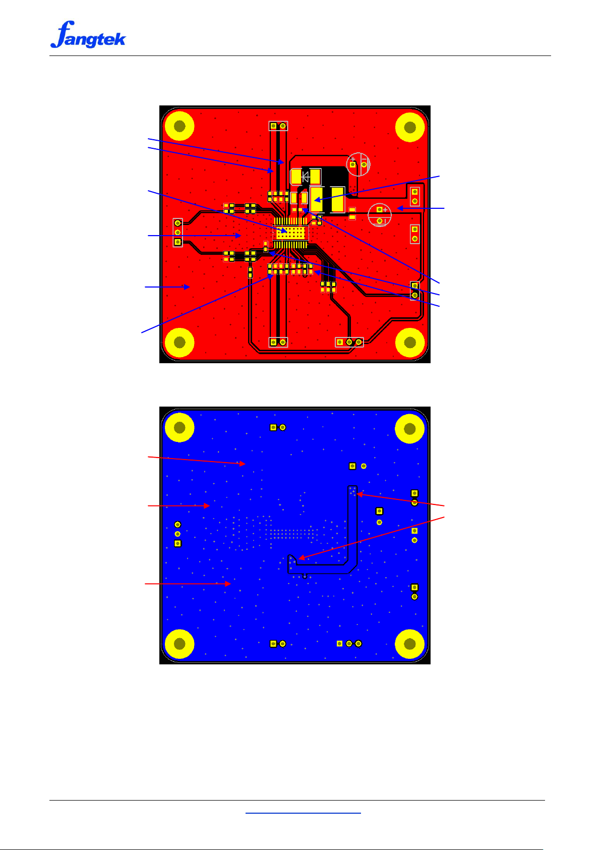
ft2925
Direct, wide traces for
audio outputs
Lots of vias underneath
the package connecting
top & bottom GND
Top layer fully
filled with GND
Wide open areas for
thermal flow. No wires
cutting the GND plane
obstructing thermal flow
Ferrite bead filter close
to audio outputs pins
Inductor & Schottky diode
tightly together and close to
LX pins
Direct, wide trace of system
power supply to inductor
Ceramic decoupling capacitors
close to associated pins (VBAT,
AVDD, BVDD, and PVDDL/R)
Lots of vias connecting top
& bottom GND planes
Bottom layer fully
filled with GND
Solid GND plane for low
impedance return path
Multiple vias connecting
PVDDL/R pins with a short
and wide trace
PCB LAYOUT EXAMPLE
Figure 33: Top Layer of Layout Example
DEC, 2017 http://www.fangtek.com.cn 23
Figure 34: Bottom Layer of Layout Example
Page 24
ft2925
CAVDD
1uF
D1 SS34
CPVDDR
1uF
CVBAT
1uF
EN
Rin
15K
LSR
SPEAKER
INR
Cin
0.22uF
ft2925
2
3
4
5
6
7
8
10
12
13
14 15
16
17
18
9
1
19
20
11
21
22
23
24
25
26
27
28
INNL
INPL
PGND
VOPL
VONL
PVDDL
AVDD
NC
ALC
SDRIVE
EN LX
LX
PGNDB
PGNDB
BVDD
VBAT
PVOUT
PVOUT
VKNEE
PVSNS
PVDDR
VONR
VOPR
PGND
INPR
INNR
AGND
INL
PVDD
RS1 10Ω
CS
0.1uF
LSL
SPEAKER
Cin 0.22uF
PVDD
CPVOUT
0.1uF
CPVOUT
22uF
Cin 0.22uF
VDD
CPVDDL
1uF
CBVDD
0.1uF
RS2 10Ω
Rin 15K
Rin
15K
VDD
+
CPVOUT
220uF
CS
22uF
L 3.3uH
Rin 15K Cin
0.22uF
INNL
RS2 10Ω
LSL
SPEAKER
Cin
0.22uF
Cin 0.22uF
Rin
15K
Rin 15K
ft2925
2
3
4
5
6
7
8
10
12
13
14 15
16
17
18
9
1
19
20
11
21
22
23
24
25
26
27
28
INNL
INPL
PGND
VOPL
VONL
PVDDL
AVDD
NC
ALC
SDRIVE
EN LX
LX
PGNDB
PGNDB
BVDD
VBAT
PVOUT
PVOUT
VKNEE
PVSNS
PVDDR
VONR
VOPR
PGND
INPR
INNR
AGND
VDD
CVBAT
1uF
Rin 15K
PVDD
Rin
15K
RS1 10Ω
D1 SS34
CBVDD
0.1uF
Cin
0.22uF
INNR
CPVDDR
1uF
CPVOUT
0.1uF
PVDD
EN
VDD
CAVDD
1uF
CPVDDL
1uF
CS
22uF
LSR
SPEAKER
CS
0.1uF
L 3.3uH
+
CPVOUT
220uF
CPVOUT
22uF
Cin 0.22uF
INPL INPR
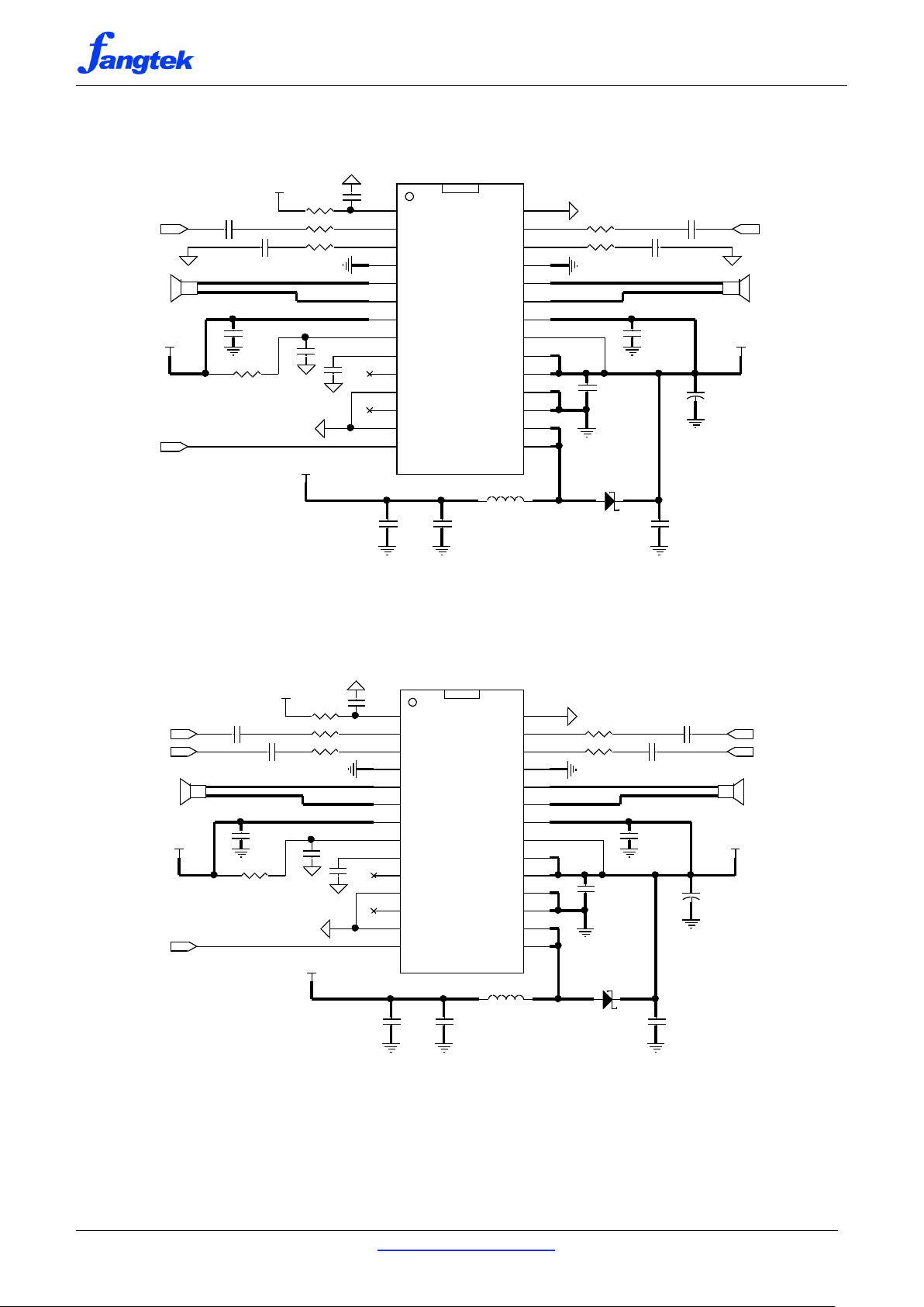
TYPICAL APPLICATION CIRCUITS
Figure 35: Single-Ended Inputs with High Efficiency Drive in ALC-2 Mode
Note: The bold lines indicate high current paths and their respective traces are required to be as wide and short as possible
on the system board for optimum performance in maximum output power, power efficiency, THD+N, and EMI emissions.
DEC, 2017 http://www.fangtek.com.cn 24
Figure 36: Differential Inputs with High Efficiency Drive in ALC-2 Mode
Page 25
ft2925
CVBAT
1uF
LSR
SPEAKER
PVDD
+
CPVOUT
220uF
CPVDDL
1uF
R1 100K
CS
0.1uF
Q1
MMBT3904
CAVDD
1uF
INR
L 3.3uH
Cin 0.22uF
Cin
0.22uF
Cin 0.22uF
PVDD
VDD
EN
Rin 15K
CBVDD
0.1uF
INL
SDRIVE
CS
22uF
RS2 10Ω
LSL
SPEAKER
Cin
0.22uF
Rin
15K
CPVOUT
0.1uF
ft2925
2
3
4
5
6
7
8
10
12
13
14 15
16
17
18
9
1
19
20
11
21
22
23
24
25
26
27
28
INNL
INPL
PGND
VOPL
VONL
PVDDL
AVDD
NC
ALC
SDRIVE
EN LX
LX
PGNDB
PGNDB
BVDD
VBAT
PVOUT
PVOUT
VKNEE
PVSNS
PVDDR
VONR
VOPR
PGND
INPR
INNR
AGND
Rin
15K
VDD
CPVOUT
22uF
Rin 15K
D1 SS34
CPVDDR
1uF
RS1 10Ω
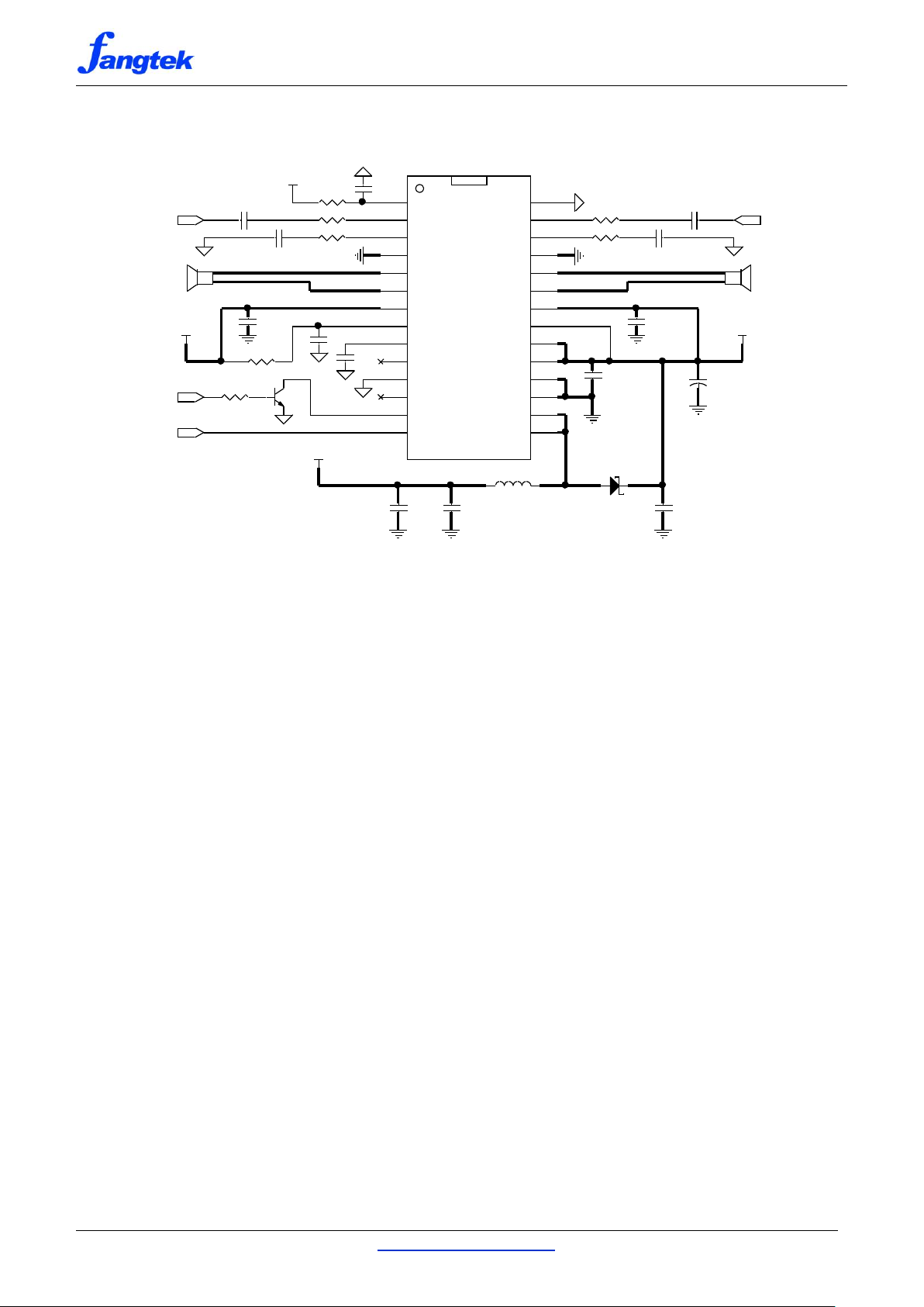
TYPICAL APPLICATION CIRCUITS (Cont’d)
Figure 37: Single-Ended Inputs with Soft Drive Control in ALC-2 Mode
Note: The bold lines indicate high current paths and their respective traces are required to be as wide and short as possible
on the system board for optimum performance in maximum output power, power efficiency, THD+N, and EMI emissions.
DEC, 2017 http://www.fangtek.com.cn 25
Page 26
ft2925
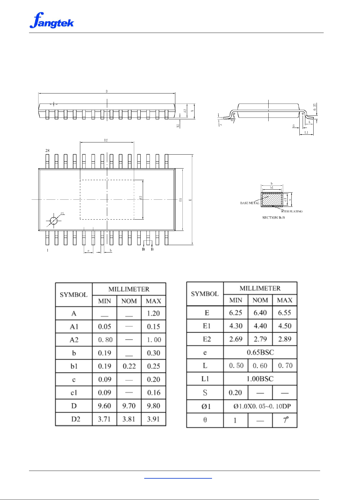
PHYSICAL DIMENSIONS
TSSOP-28L PACKAGE OUTLINE DIMENSIONS
DEC, 2017 http://www.fangtek.com.cn 26
Page 27

ft2925
IMPORTANT NOTICE
1. Disclaimer: The information in document is intended to help you evaluate this product. Fangtek, LTD.
makes no warranty, either expressed or implied, as to the product information herein listed, and reserves
the right to change or discontinue work on this product without notice.
2. Life support policy: Fangtek’s products are not authorized for use as critical components in life support
devices or systems without the express written approval of the president and general counsel of Fangtek
Inc. As used herein
Life support devices or systems are devices or systems which, (a) are intended for surgical implant into the
body, or (b) support or sustain life, and whose failure to perform when properly used in accordance with
instructions for use provided in the labeling, can be reasonably expected to result in a significant injury to
the user.
A critical component is any component of a life support device or system whose failure to perform can be
reasonably expected to cause the failure of the life support device or system, or to affect its safety or
effectiveness.
3. Fangtek assumes no liability for incidental, consequential or special damages or injury that may result
from misapplications or improper use or operation of its products
4. Fangtek makes no warranty or representation that its products are subject to intellectual property license
from Fangtek or any third party, and Fangtek makes no warranty or representation of non-infringement with
respect to its products. Fangtek specifically excludes any liability to the customer or any third party arising
from or related to the products’ infringement of any third party’s intellectual property rights, including
patents, copyright, trademark or trade secret rights of any third party.
5. The information in this document is merely to indicate the characteristics and performance of Fangtek
products. Fangtek assumes no responsibility for any intellectual property claims or other problems that may
result from applications based on the document presented herein. Fangtek makes no warranty with respect
to its products, express or implied, including, but not limited to the warranties of merchantability, fitness for
a particular use and title.
6. Trademarks: The company and product names in this document may be the trademarks or registered
trademarks of their respective manufacturers. Fangtek is trademark of Fangtek, LTD.
CONTACT INFORMATION
Fangtek Electronics (Shanghai) Co., Ltd
Room 501A, Lane 198, Zhangheng Road
Zhangjiang Hi-tech Park, Pudong District
Shanghai, China, 201204
Tel: +86-21-61631978
Fax: +86-21-61631981
Website:
www.fangtek.com.cn
DEC, 2017 http://www.fangtek.com.cn 27
 Loading...