

Page 1
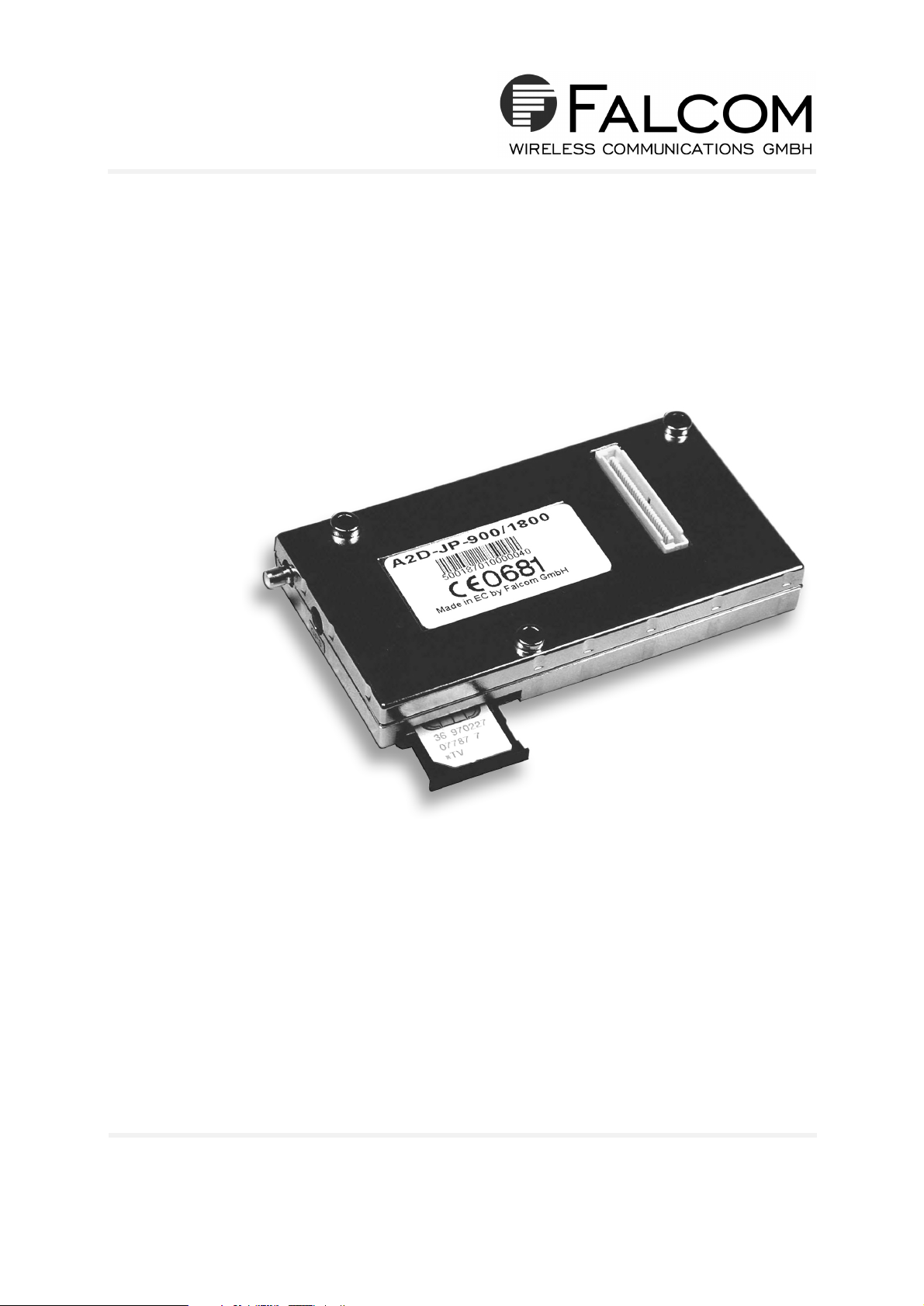
Description
Embedded GSM/GPS–Module A2D–JP
Page 2

©
T
G
t
c
A
f
c
A
2001
he information in this document is copyrighted for Falcom Wireless Communications
mbH. Any reproduction of this User Manual in whole or in part, electronic storage or
ranslation in other languages are permitted only with the prior written consent of Fal-
om Wireless Communications GmbH.
ll details of FALCOM’s products, particularly those in catalogues, in printed or other
orm, contain diagrams and details of products and performances which are not gua-
ranteed features, but approximations. In respect of these, only the agreements in the
ontract of supply are valid.
ll rights reserved.
Page 3

Description Contents
Contents
1 Introduction. . . . . . . . . . . . . . . . . . . . . . . . . . . . . . . . . . . . . . . . . . 2
1.1 General . . . . . . . . . . . . . . . . . . . . . . . . . . . . . . . . . . . . . . . . . . . . . . . . . . . . . .2
1.2 Used abbreviations . . . . . . . . . . . . . . . . . . . . . . . . . . . . . . . . . . . . . . . . . . . . .4
1.3 Related documents . . . . . . . . . . . . . . . . . . . . . . . . . . . . . . . . . . . . . . . . . . . . .5
1.4 Alert symbols used . . . . . . . . . . . . . . . . . . . . . . . . . . . . . . . . . . . . . . . . . . . . .5
2 Security . . . . . . . . . . . . . . . . . . . . . . . . . . . . . . . . . . . . . . . . . . . . 6
2.1 General information. . . . . . . . . . . . . . . . . . . . . . . . . . . . . . . . . . . . . . . . . . . . .6
2.2 Exposure to RF energy . . . . . . . . . . . . . . . . . . . . . . . . . . . . . . . . . . . . . . . . . .6
2.3 Efficient modem operation. . . . . . . . . . . . . . . . . . . . . . . . . . . . . . . . . . . . . . . .7
2.4 Antenna care and replacement . . . . . . . . . . . . . . . . . . . . . . . . . . . . . . . . . . . .7
2.5 Driving . . . . . . . . . . . . . . . . . . . . . . . . . . . . . . . . . . . . . . . . . . . . . . . . . . . . . . .8
2.6 Electronic devices . . . . . . . . . . . . . . . . . . . . . . . . . . . . . . . . . . . . . . . . . . . . . .8
2.7 Vehicle electronic equipment. . . . . . . . . . . . . . . . . . . . . . . . . . . . . . . . . . . . . .8
2.8 Medical electronic equipment . . . . . . . . . . . . . . . . . . . . . . . . . . . . . . . . . . . . .8
2.9 Aircraft . . . . . . . . . . . . . . . . . . . . . . . . . . . . . . . . . . . . . . . . . . . . . . . . . . . . . . .8
2.10 Children . . . . . . . . . . . . . . . . . . . . . . . . . . . . . . . . . . . . . . . . . . . . . . . . . . . . . .8
2.11 Blasting areas . . . . . . . . . . . . . . . . . . . . . . . . . . . . . . . . . . . . . . . . . . . . . . . . .9
2.12 Potentially explosive atmospheres . . . . . . . . . . . . . . . . . . . . . . . . . . . . . . . . .9
2.13 Non-ionising radiation . . . . . . . . . . . . . . . . . . . . . . . . . . . . . . . . . . . . . . . . . . .9
3 Safety standards . . . . . . . . . . . . . . . . . . . . . . . . . . . . . . . . . . . . 10
4 Technical data . . . . . . . . . . . . . . . . . . . . . . . . . . . . . . . . . . . . . . 11
5GSM–modem . . . . . . . . . . . . . . . . . . . . . . . . . . . . . . . . . . . . . . . 15
5.1 General . . . . . . . . . . . . . . . . . . . . . . . . . . . . . . . . . . . . . . . . . . . . . . . . . . . . .15
5.1.1 GSM capability . . . . . . . . . . . . . . . . . . . . . . . . . . . . . . . . . . . . . . . . . . . . . . .15
5.1.2 GSM data services . . . . . . . . . . . . . . . . . . . . . . . . . . . . . . . . . . . . . . . . . . . .15
5.1.3 RF characteristics . . . . . . . . . . . . . . . . . . . . . . . . . . . . . . . . . . . . . . . . . . . . .15
5.1.4 SIM card reader. . . . . . . . . . . . . . . . . . . . . . . . . . . . . . . . . . . . . . . . . . . . . . .16
5.1.5 RS 232 . . . . . . . . . . . . . . . . . . . . . . . . . . . . . . . . . . . . . . . . . . . . . . . . . . . . .16
5.1.6 Possible external devices . . . . . . . . . . . . . . . . . . . . . . . . . . . . . . . . . . . . . . .16
5.2 Special functionality pins . . . . . . . . . . . . . . . . . . . . . . . . . . . . . . . . . . . . . . . .16
5.2.1 Firmware download procedure . . . . . . . . . . . . . . . . . . . . . . . . . . . . . . . . . . .19
5.2.2 Resetting the GSM–module by AT+CFUN=1,1. . . . . . . . . . . . . . . . . . . . . . .19
5.3 GSM 07.05. and 07.07. commands. . . . . . . . . . . . . . . . . . . . . . . . . . . . . . . .19
A2D–JP Version 1.03 Side 1
Page 4

Description Contents
5.3.1 General AT commands . . . . . . . . . . . . . . . . . . . . . . . . . . . . . . . . . . . . . . . . .20
5.3.2 SMS AT commands (GSM 07.05). . . . . . . . . . . . . . . . . . . . . . . . . . . . . . . . .20
5.3.3 GSM AT commands (GSM 07.07). . . . . . . . . . . . . . . . . . . . . . . . . . . . . . . . .21
6 GPS receiver . . . . . . . . . . . . . . . . . . . . . . . . . . . . . . . . . . . . . . . 22
6.1 General . . . . . . . . . . . . . . . . . . . . . . . . . . . . . . . . . . . . . . . . . . . . . . . . . . . . .22
6.2 Product overview. . . . . . . . . . . . . . . . . . . . . . . . . . . . . . . . . . . . . . . . . . . . . .23
6.2.1 GPS receiver architecture . . . . . . . . . . . . . . . . . . . . . . . . . . . . . . . . . . . . . . .23
6.2.2 Product applications . . . . . . . . . . . . . . . . . . . . . . . . . . . . . . . . . . . . . . . . . . .24
6.3 Technical description. . . . . . . . . . . . . . . . . . . . . . . . . . . . . . . . . . . . . . . . . . .24
6.3.1 General information. . . . . . . . . . . . . . . . . . . . . . . . . . . . . . . . . . . . . . . . . . . .24
6.3.2 Hardware interface . . . . . . . . . . . . . . . . . . . . . . . . . . . . . . . . . . . . . . . . . . . .25
6.3.2.1 Configuration and timing signals . . . . . . . . . . . . . . . . . . . . . . . . . . . . . . . . . .25
6.3.3 Serial communication signals . . . . . . . . . . . . . . . . . . . . . . . . . . . . . . . . . . . .26
6.3.4 DC input signals . . . . . . . . . . . . . . . . . . . . . . . . . . . . . . . . . . . . . . . . . . . . . .28
6.3.5 Software interface . . . . . . . . . . . . . . . . . . . . . . . . . . . . . . . . . . . . . . . . . . . . .28
6.3.5.1 Binary data message. . . . . . . . . . . . . . . . . . . . . . . . . . . . . . . . . . . . . . . . . . .29
6.3.5.2 NMEA data message. . . . . . . . . . . . . . . . . . . . . . . . . . . . . . . . . . . . . . . . . . .31
7 A2D-JP evaluation board . . . . . . . . . . . . . . . . . . . . . . . . . . . . . . 32
A2D–JP Version 1.03 Side 2
Page 5

Description List of figures
List of figures
Figure 1: Drawing of A2D–JP . . . . . . . . . . . . . . . . . . . . . . . . . . . . . . . . . . . . . . . . . . . .2
Figure 2: Technical drawing of A2D–JP . . . . . . . . . . . . . . . . . . . . . . . . . . . . . . . . . . . .3
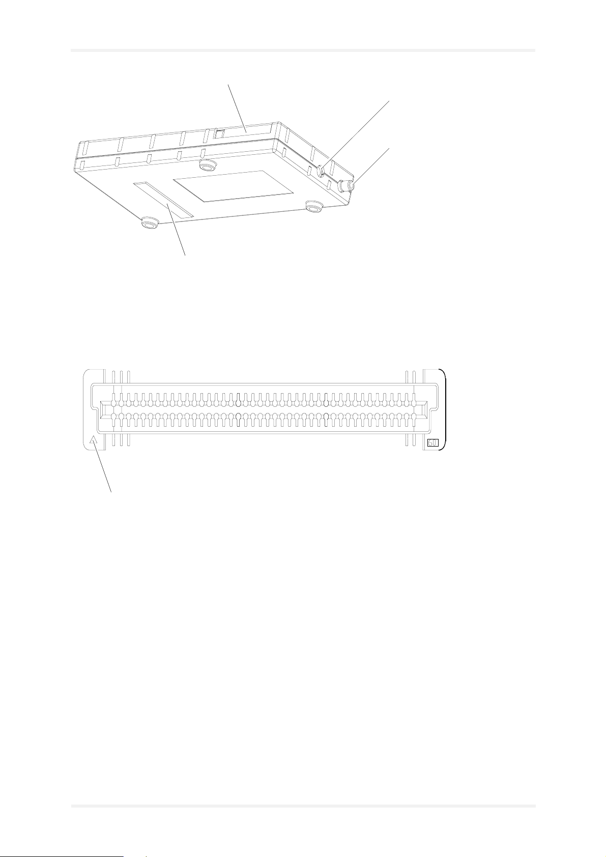
Figure 3: Interface connections . . . . . . . . . . . . . . . . . . . . . . . . . . . . . . . . . . . . . . . . .12
Figure 4: Interface A: 60pin connector AMP 177984-2 . . . . . . . . . . . . . . . . . . . . . . .12
Figure 5: GPIO 1
Figure 6: Sample-application SIMPREK. . . . . . . . . . . . . . . . . . . . . . . . . . . . . . . . . . .18
Figure 7: GPS receiver architecture . . . . . . . . . . . . . . . . . . . . . . . . . . . . . . . . . . . . . .23
Figure 8: The A2D-JP evaluation board . . . . . . . . . . . . . . . . . . . . . . . . . . . . . . . . . . .32
Flash_LED . . . . . . . . . . . . . . . . . . . . . . . . . . . . . . . . . . . . . . . . .17
→→→→
A2D–JP Version 1.03 Side 3
Page 6

Description Versions
Versions
Version number Author Changes
V 1.00 M. Menz Initial version
V 1.01 G. Buch Chip set of RAM/Flash changed
(GPS)
V 1.02 G. Buch Reset chip changed (GPS)
V 1.03 G. Buch Layout of L2/R35/C2/D13/C27
changed
Ground GSM-antenna changed
A2D–JP Version 1.03 Side 1
Page 7
Description Introduction
1Introduction
1.1 General
This manual is focussed on the embedded GSM/GPS-module of the
FALCOM A2D-JP series from FALCOM GmbH. It contains some
information about the FALCOM GSM module and the FALCOM
GPS-module based on the CONEXANT Zodiac 2000 chip set.
Information furnished herein by FALCOM GmbH is believed to
be accurate and reliable. However, no responsibility is assumed for its use. Also the information contained herein is subject to change without notice.
Users are advised to proceed quickly to the „Security“ chapter
and read the hints carefully.
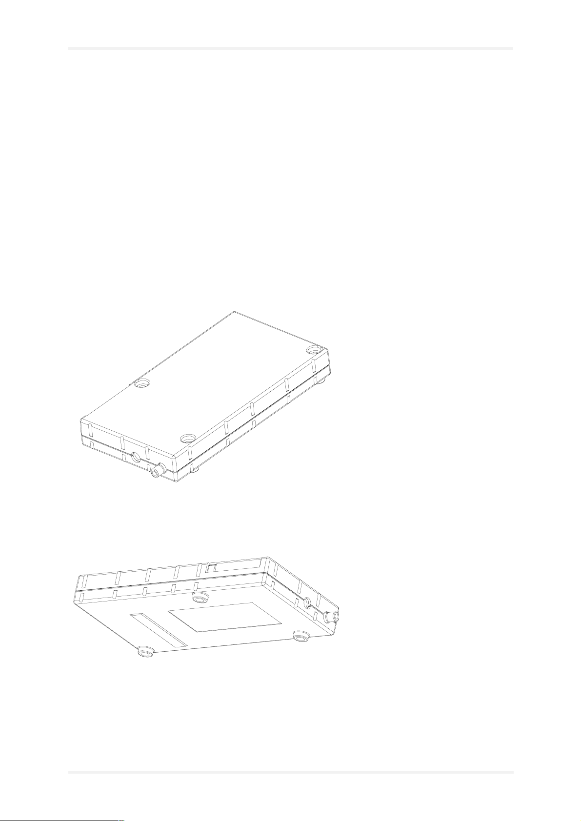
Figure 1: Drawing of A2D–JP
A2D–JP Version 1.03 Side 2
Page 8
Description Introduction
16.35
Ø2.7
(3x)
6.65
10.15
20
15
3140
6.85
13.3
12.1 max
2
4.65
1.65
25.5 57.15
2.8
5
Ø
1.7 tief
53.8±0.15
73.2±0.15
90.2±0.3
(94.7)
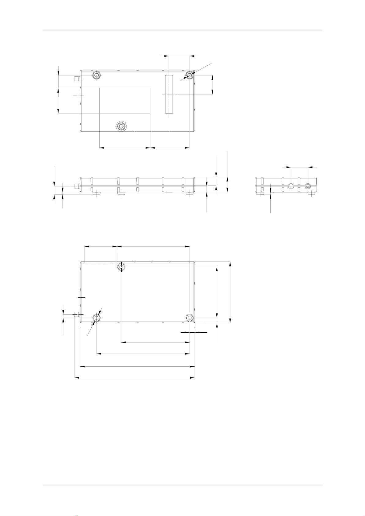
Figure 2: Technical drawing of A2D–JP
40.3±0.15
48.4±0.25
4
4
A2D–JP Version 1.03 Side 3
Page 9

Description Introduction
1.2 Used abbreviations
Abbreviation Meaning
CTS Clear To Send signal from Dent
DGPS Differential GPS
DOP Dilution of Precision
ECEF Earth-Centred Earth-Fixed Coordinate system
EEPROM Memory for parameter
ETSI European Telecommunications Standards Institute
GSM Global System for Mobile communications
GPS Global Positioning System
GGA GPS Fixed Data
HDOP Horizontal DOP
IMEI International Mobile station Equipment Identity
ME Mobile Equipment
NMEA National Maritime Electronics Association
PIN Personal Identification Number
PLMN Public Land Mobile Network
PRN Pseudorandom Noise Number–The Identity of GPS satellites
PUK Personal Unblocking Key
RP Receive Protocol
RTC Real Time Clock
RTCM Radio Technical Commission for Maritime Services
RXD Data input
RXQUAL Received Signal Quality
SIM Subscriber Identity Module
SMS Short Message Service
SMS/PP Short Message Service/Point-to-Point
SRAM Static Random Access Memory
TA Terminal Adapter
TE Terminal Equipment
TP Transmit Protocol
TTFF Time To First Fix
TXD Data output
Table 1: Abbreviations
A2D–JP Version 1.03 Side 4
Page 10

Description Introduction
1.3 Related documents
[1] ETSI GSM 07.05 "Use of Data Terminal Equipment - Data Circuit terminating
Equipment interface for Short Message Service and Cell
Broadcast Service"
[2] ETSI GSM 07.07 "AT command set for GSM Mobile Equipment"
[3] ITU-T V.25ter "Serial asynchronous automatic dialling and control"
http://
[4] Zodiac GPS receiver Family Designers' Guide
www.falcom.de/service/downloads
[5] GPS Chipset-Zodiac 2000
[6] Serial Data I/O Interface see chapter 5 of [4]
http://
www.falcom.de/service/downloads
1.4 Alert symbols used
Alerts the user to potential safety risks.
!
Indicates important information and tips.
A2D–JP Version 1.03 Side 5
Page 11

Description Security
2 Security
IMPORTANT FOR THE EFFICIENT AND SAFE OPERATION OF
YOUR GSM–MODEM, READ THIS INFORMATION BEFORE
USE!
Your embedded GSM/GPS–modem is one of the most exciting and
innovative electronic products ever developed. With it you can stay
in contact with your office, your home, emergency services, and
others, wherever service is provided.
This chapter contains important information for the safe and reliable
use of the GPS receiver. Please read this chapter carefully before
starting to use the GPS receiver.
2.1 General information
Your modem utilises the GSM standard for cellular technology. GSM
is a newer radio frequency („RF“) technology than the current FM
technology that has been used for radio communications for decades. The GSM standard has been established for use in the European community and elsewhere.
Your modem is actually a low power radio transmitter and receiver.
It sends out and receives radio frequency energy. When you use
your modem, the cellular system handling your calls controls both
the radio frequency and the power level of your cellular modem.
The Global Positioning System uses satellite navigation, an entirely
new concept in navigation. GPS has become established in many
areas, for example, in civil aviation or deep-sea shipping. It is making deep inroads in vehicle manufacturing, and long before everyone of us will use it in one way or another.
The GPS system is operated by the government of the United States
of America, which also has sole responsibility for the accuracy and
maintenance of the system. The system is constantly being improved and may entail modifications effecting the accuracy and performance of the GPS equipment.
2.2 Exposure to RF energy
There has been some public concern about possible health effects
of using GSM modem. Although research on health effects from RF
energy has focused for many years on the current RF technology,
scientists have begun research regarding newer radio technologies,
such as GSM. After existing research had been reviewed, and after
compliance to all applicable safety standards had been tested, it has
been concluded that the product is fit for use.
A2D–JP Version 1.03 Side 6
Page 12

Description Security
If you are concerned about exposure to RF energy there are things
you can do to minimise exposure. Obviously, limiting the duration of
your calls will reduce your exposure to RF energy. In addition, you
can reduce RF exposure by operating your cellular modem efficiently by following the guidelines below.
2.3 Efficient modem operation
In order to operate your modem at the lowest power level, consistent
with satisfactory call quality please take note of the following hints.
If your modem has an extendible antenna, extend it fully. Some models allow you to place a call with the antenna retracted. However
your modem operates more efficiently with the antenna fully extended.
Do not hold the antenna when the modem is „IN USE“. Holding the
antenna affects call quality and may cause the modem to operate at
a higher power level than needed.
2.4 Antenna care and replacement
Do not use the modem with a damaged antenna. If a damaged antenna comes into contact with the skin, a minor burn may result. Replace a damaged antenna immediately. Consult your manual to see
if you may change the antenna yourself. If so, use only a manufacturer-approved antenna. Otherwise, have your antenna repaired by
a qualified technician.
Use only the supplied or approved antenna. Unauthorised antennas, modifications or attachments could damage the modem and
may contravene local RF emission regulations or invalidate type approval.
Operate the GPS receiver with a connected antenna and make sure
that there is no obstruction between the receiver and the satellite.
Make absolutely sure that the antenna socket or antenna cable is
not shorted as this would render the GPS receiver dysfunctional.
Do not use the receiver with a damaged antenna. Replace a damaged antenna without delay. Use only a manufacturer-approved antenna. Use only the supplied or an approved antenna with your GPS
receiver. Antennas from other manufacturers which are not authorized by the supplier can damage the GPS receiver. Technical modifications and additions may contravene local radio-frequency emission regulations or invalidate the type approval.
Authorized GPS antennas:
FALCOM ANT 006 (active)
A2D–JP Version 1.03 Side 7
Page 13

Description Security
2.5 Driving
Check the laws and regulations on the use of cellular devices in the
area where you drive. Always obey them. Also, when using your modem while driving, please pay full attention to driving, pull off the
road and park before making or answering a call if driving conditions
so require. When applications are prepared for mobile use they
should fulfil road-safety instructions of the current law!
2.6 Electronic devices
Most electronic equipment, for example in hospitals and motor vehicles is shielded from RF energy. However RF energy may affect
some malfunctioning or improperly shielded electronic equipment.
2.7 Vehicle electronic equipment
Check your vehicle manufacturer's representative to determine if
any on board electronic equipment is adequately shielded from RF
energy.
2.8 Medical electronic equipment
Consult the manufacturer of any personal medical devices (such as
pacemakers, hearing aids, etc...) to determine if they are adequately
shielded from external RF energy.
Turn your modem OFF in health care facilities when any regulations
posted in the area instruct you to do so. Hospitals or health care facilities may be using RF monitoring equipment.
2.9 Aircraft
Turn your modem OFF before boarding any aircraft.
Use it on the ground only with crew permission.
Do not use it in the air.
To prevent possible interference with aircraft systems, Federal Aviation Administration (FAA) regulations require you to have permission from a crew member to use your modem while the plane is on the
ground. To prevent interference with cellular systems, local RF regulations prohibit using your modem whilst airborne.
2.10 Children
Do not allow children to play with your modem. It is not a toy. Children could hurt themselves or others (by poking themselves or
others in the eye with the antenna, for example). Children could damage the modem, or make calls that increase your modem bills.
A2D–JP Version 1.03 Side 8
Page 14

Description Security
2.11 Blasting areas
To avoid interfering with blasting operations, turn your unit OFF
when in a "blasting area" or in areas posted : „turn off two-way radio“. Construction crew often use remote control RF devices to set
off explosives.
2.12 Potentially explosive atmospheres
Turn your modem OFF when in any area with a potentially explosive
atmosphere. It is rare, but your modem or its accessories could generate sparks. Sparks in such areas could cause an explosion or
fire resulting in bodily injury or even death.
Areas with a potentially explosive atmosphere are often, but not always, clearly marked. They include fuelling areas such as petrol stations; below decks on boats; fuel or chemical transfer or storage facilities; and areas where the air contains chemicals or particles, such
as grain, dust, or metal powders.
Do not transport or store flammable gas, liquid, or explosives, in the
compartment of your vehicle which contains your modem or accessories.
Before using your modem in a vehicle powered by liquefied petroleum gas (such as propane or butane) ensure that the vehicle complies with the relevant fire and safety regulations of the country in
which the vehicle is to be used.
2.13 Non-ionising radiation
As with other mobile radio transmitting equipment users are advised that for satisfactory operation and for the safety of personnel,
it is recommended that no part of the human body be allowed to
come too close to the antenna during operation of the equipment.
The radio equipment shall be connected to the antenna via a nonradiating 50Ohm coaxial cable.
The antenna shall be mounted in such a position that no part of the
human body will normally rest close to any part of the antenna. It is
also recommended to use the equipment not close to medical devices as for example hearing aids and pacemakers.
A2D–JP Version 1.03 Side 9
Page 15

Description Safety standards
3 Safety standards
This GSM/GPS-modem complies with all applicable RF safety
standards.
The embedded GMS/GPS-modem meets the safety standards for
RF receivers and the standards and recommendations for the protection of public exposure to RF electromagnetic energy established
by government bodies and professional organizations, such as directives of the European Community, Directorate General V in matters of radio frequency electromagnetic energy.
A2D–JP Version 1.03 Side 10
Page 16
Description Technical data
4 Technical data
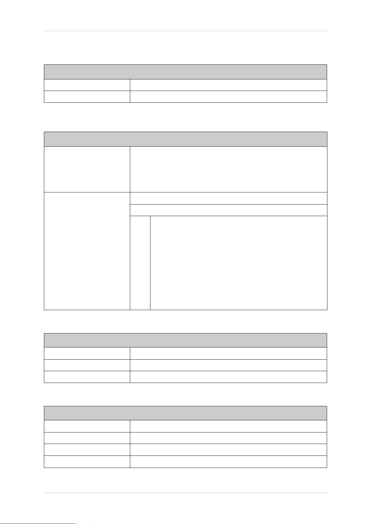
General specifications
Dimensions 95 mm x 50 mm x 15 mm (B x W x H)
Weight 60 g
Table 2: General specifications
Power supply
GPS VC3 3.3 V DC ±5 %
Max. 190 mA Operate
VBAT 3 V DC ±0,25 V
Max. 40 µA for „Keep Alive“
Preamp. Power 3,3 V DC – 6 V DC ±5 %
Max. 50 mA
GSM VC5 5,0 V DC ± 5 %
Average current (in mA at 5V nominal):
0,015
17*
30*
260*
350*
Table 3: Power supply
Operation -20 °C to +55 °C
Transportation -40 °C to +70 °C
Storage -25 °C to +70 °C
Table 4: Temperature limits
in OFF mode 2 (EN pulled to LOW, the internal regulator is switched
off)
in OFF mode 1 (AT+CPOF was issued and SOFT_ON was set to
LOW, the internal regulator is still working)
in idle mode (base station sends at -85 dBm)
in transmit mode at power level 7
in transmit mode at power level 5 (Maximum)
* Serial interface is applied and working.
Temperature limits
Interface specifications
Interface A 60pin connector AMP 177984-2
Interface B GPS 50 Ω MCX female, for active 3 V GPS antenna
Interface C GSM 50 Ω, SMB male
Interface D SIM card reader for small SIM cards (3V)
Table 5: Interface specifications
A2D–JP Version 1.03 Side 11
Page 17
Description Technical data
A
B
C
D
Figure 3: Interface connections
1
Pin No. 1
Figure 4: Interface A: 60pin connector AMP 177984-2
60
A2D–JP Version 1.03 Side 12
Page 18

Description
CorrectionPinconfigurationAMP177984-2
Pin GSM–modem Description Level
1 MICP15 Microphone1positive differentialinp.
2 MICN15 Microphone1negative differentialinp.
3 SPKP2 Speaker1positive differentialout.
4 SPKN2 Speaker1negative differentialout.
5 DTR RS-232DataTerm.Ready CMOS2,8Vinp.
6 CTS RS-232ClearToSend CMOS2,8Vout.
7 DSR RS-232DataSetReady CMOS2,8Vout.
8 RTS RS-232ReadyToSend CMOS2,8Vinp.
9 RI RS-232RingIndicator CMOS2,8Vout.
10 DCD RS-232DataCarrierDetect CMOS2,8Vout.
11 SOFTON Turnphoneon CMOS2,8Vinp.
12 RINGPWM RingerInterface CMOS2,8Vout.
13 TX RS-232TransmitData CMOS2,8Vout.
14 RX RS-232ReceiveData CMOS2,8Vinp.
15 Free
16 RESETGSM Reset-ActiveLow SCHMITT
17 Free
18 VCCRTC RTCback-upbatt.Supply inp.
19 Free
20 Free
21 Free
22 Free
23 VC5 Powersupply 5VDC
24 VC5 Powersupply 5VDC
25 VC5 Powersupply 5VDC
26 VC5 Powersupply 5VDC
27 GPIO1 Generalpurposein/out CMOS2,8V
28 VC5 Powersupply 5VDC
29 Free
30 EN InternalPowerenable CMOS2,8Vinp.
31 GROUND
32 GROUND
33 GROUND
Table1:PinconfigurationAMP177984-2,GSM-modem
A2D–JP Version1.03 Side13
Page 19

Description
Pin GSM–modem Description Level
34 GROUND
35 SIMPREK SIMpresentforexternalcard CMOS2,8Vinp.
36 GROUND
37 SIMDATA SIMData inp./out.
38 SIMVCC SIMCardpowersupply 3VDC
39 SIMRST SIMReset inp.
40 SIMCLK SIMClock out.
Table1:PinconfigurationAMP177984-2,GSM-modem
Pin GPSreceiver Description Level
41 TMARK 1PPStimeMarkOutput CMOS3,3Vout.
42 10KHZUTC 10kHzClock CMOS3,3Vout.
43 GROUND
44 GROUND
45 SDI2 Serial2DataInput CMOS3,3Vinp.
46 GROUND
47 GROUND
48 SDO2 Serial2DataOutput CMOS3,3Vout.
49 SDO1 Serial1DataOutput CMOS3,3Vinp.
50 SDI1 Serial1DataInput CMOS3,3Vout.
51 WHEEL_TICK ReservedforWheelin
52 GROUND
53 DIRECTION NMEAProtocolselect Low
54 DSP_GPIO3 ROMdefaultselect Low
55 M-RST MasterResetInput Low
56 GYRO_IN ReservedforGyro_in
57 VBATT_RTC BatteryBackupInput 3VDC
58 3,3VDC PrimaryDCPower 3,3VDC
59 PREAMP_POWER PreamplifierPower 3,3VDC–6VDC
60 3,3VDC PrimaryDCPower 3,3VDC
Table2:PinconfigurationAMP177984-2,GPSreceiver
A2D–JP Version1.03 Side14
Page 20

Description GSM–modem
5GSM–modem
5.1 General
5.1.1 GSM capability
E-GSM and DCS (GSM ETSI Phase I and II)
5.1.2 GSM data services
300 … 14400 BPS, asynchronous, transparent and non-transparent
(V.21, V.22, V.23, V.22bis, V.26ter, V.32, V.34, V.110)
5.1.3 RF characteristics
Receiver
EGSM Sensitivity
DCS Sensitivity
Selectivity @ 200 kHz > +9 dBc
Selectivity @ 400 kHz > +41 dBc
Dynamic range 62 dB
Intermodulation > -43 dBm
Co-channel rejection ≥ 9 dBc
Table 8: Receiver
Maximum output power (EGSM) 33 dBm ±2 dB
Maximum output power (DCS) 30 dBm ±2 dB
Minimum output power (EGSM) 5 dBm ±5 dB
Minimum output power (DCS) 0 dBm ±5 dB
H2 level ≤ 30 dBm
H3 level ≤ 30 dBm
Noise in 925 - 935 MHz ≤ 67 dBm
< −
< −
104 dBm
100 dBm
Transmitter
Noise in 935 - 960 MHz ≤ 79 dBm
Noise in 1805 - 1880 MHz ≤ 71 dBm
Phase error at peak power < 5 ° RMS
Frequency error ±0.1ppm max
Tab le 9: Tr a nsmit ter
A2D–JP Version 1.03 Side 15
Page 21

Description GSM–modem
5.1.4 SIM card reader
Internal, for small SIM cards (3 V)
External, 10 … 15 cm maximum cable length
5.1.5 RS 232
RS 232
2.8 V RX, TX, RTS, CTS, DTR, DSR, DCD, RI
300..115200 Baud rates for serial link (2400 … 19200 with auto-bauding)
Table 10: RS 232
5.1.6 Possible external devices
Audio
ΩΩΩΩ
2 K
differential
2 V Microphone 1 bias voltage
0,5 mA Microphone 1 input current
2 K
ΩΩΩΩ
differential
2 V Microphone 2 bias voltage
0,5 mA Microphone 2 input current
ΩΩΩΩ
> 50
(<1nF)
ΩΩΩΩ
> 50
(<1nF)
Table 11: Audio
Microphone 1 impedance
Microphone 2 impedance
Speaker 1 impedance
Speaker 2 impedance
5.2 Special functionality pins
Table 6 and Tabl e7 show the pin-configuration of the AMP
177984-2.
In these tables CMOS means 2.8 V. You may use a 3 V or 3.3 V
CMOS level logic (never 5 V) on the 2.8 V I/O's. However, it is required to add serial resistance on all the lines you will use (typical value:
from 4.7 to 10 KΩ).
There are a few pins needed for the operation of the module. The
handling of that pins is described as follows.
A2D–JP Version 1.03 Side 16
Page 22
Description GSM–modem
Pin 30 (EN)
This signal is an input of the internal voltage regulator.
Pull to LOW to switch the voltage regulator off (for minimum
❐
current consumption).
Pull to HIGH or leave the signal open if EN is not used.
❐
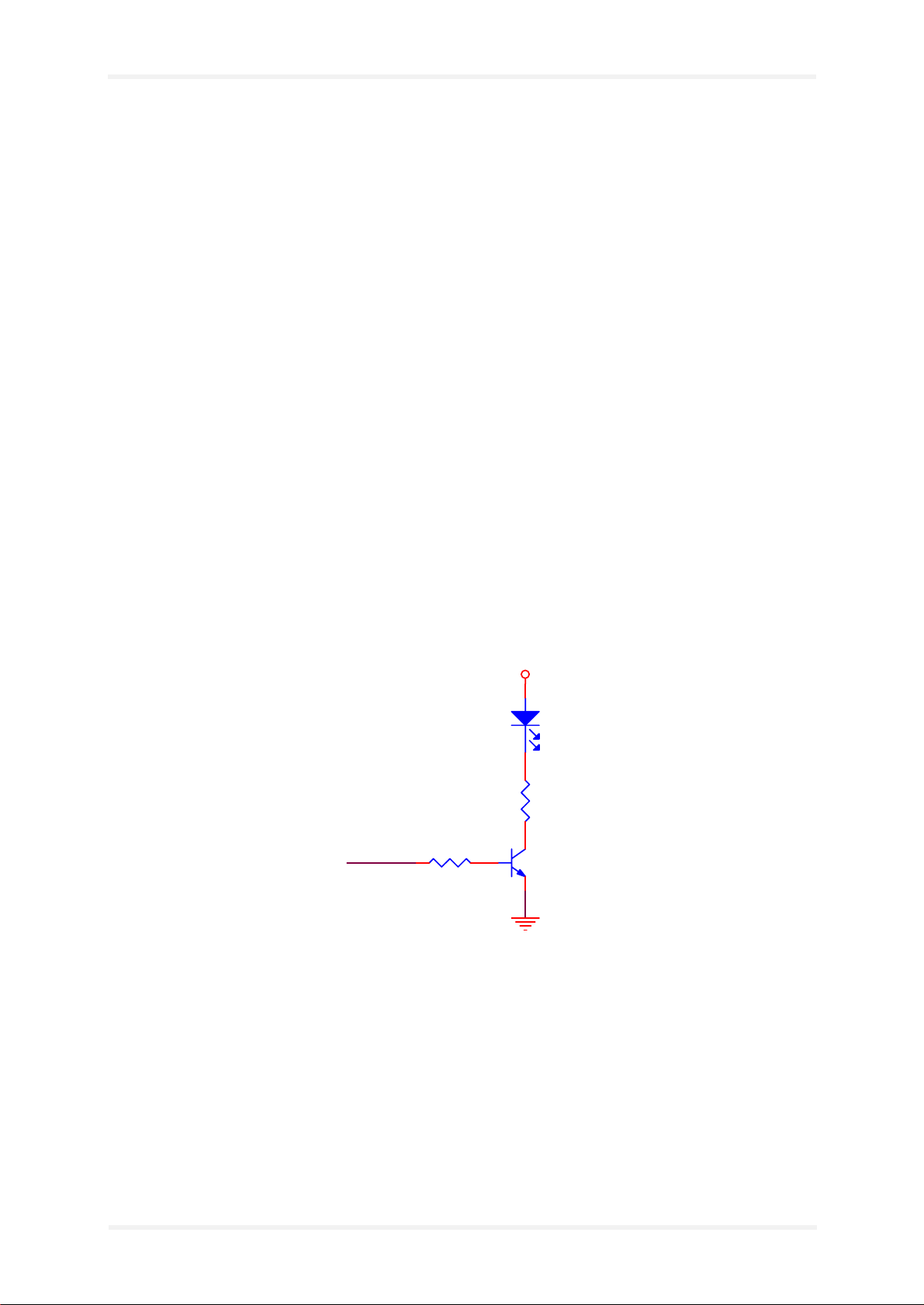
Pin 27 (GPIO 1 →→→→ Flash_LED)
This signal can be used to show the current status of the module:
If GPIO 1 is LOW then the module is off.
❐
If it is continuously HIGH then module is on, but not registered
❐
into a network.
If GPIO 1 is flashing in a 2sec period then the module is on and
❐
registered into a network.
If it flashes in a 1sec period then the module is on and a call is
❐
in progress (incoming or outgoing).
Figure 5: GPIO 1
GPIO 1 can be an input into a controller (here it needs to be driven
by an open collector circuit) or used together with a LED (see picture
below):
→→→→ Flash_LED
GPIO 1
R1
47K
VCC 3V
D1
LED
R2
330
Q1
NPN
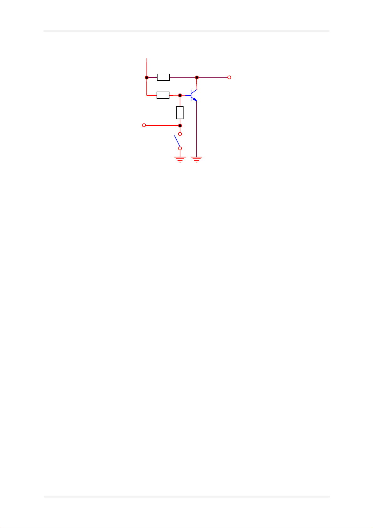
Pin 35 (SIMPREK)
This signal needs to be driven by an open collector circuit. It is used
by the module's firmware to detect a SIM card exchange when the
module is online. A high to low transition means SIM card is inserted
and the module will be able to accept the AT+CPIN command. A low
to high transition means SIM card has been removed, the mo-dule
will de-register from the network and show the unsolicited error code
CME ERROR: 10.
A2D–JP Version 1.03 Side 17
Page 23
Description GSM–modem
DVCC
10 K
SIMPRES
BC817
100 K
1 K
SIMPREK
Figure 6: Sample-application SIMPREK
Pin 16 (RESET GSM)
This signal needs to be driven by an external open collector circuit.
To issue a hardware reset pull the signal to LOW for a mini-
❐
mum of 100 ms.
Pull the signal to HIGH or leave it open for normal operation.
❐
Pin 11 (SOFT_ON)
This signal needs to be driven by an external open collector circuit.
For switching the module on (external power must be connec-
❐
ted!) set the SOFT_ON signal to HIGH for approx. 3 sec. The
signal can be left HIGH until module shall be switched off.
For switching the module off the commands AT+CPOF or
❐
AT+CFUN=0 have to be issued.
– If SOFT_ON is HIGH then only the RF part of the module
is off, but the AT command set is still working (AT+CFUN=1
can be used to wake up the RF part again) →→→→ the
Flash_LED stays HIGH.
– If SOFT_ON is LOW then the complete GSM engine goes
OFF →→→→ the Flash_LED goes LOW. Some small power consumption will be still there, use the EN pin to avoid that.
It is not recommended to switch the module on and off by means of
the power supply (e. g. by tying the SOFT_ON constantly to HIGH).
The module will so have no possibility to de-register correctly from
the network and this will cause problems at the next attempt to register.
A2D–JP Version 1.03 Side 18
Page 24

Description GSM–modem
Pin 18 (VCCRTC)
This is the Pin for a +3 V DC back-up battery supply for the real-timeclock.
5.2.1 Firmware download procedure
The download procedure will be documented together with the firmware release on the FALCOM homepage (http://www.falcom.de
).
5.2.2 Resetting the GSM–module by AT+CFUN=1,1
If the GSM software is still running, while the user feels the need to
reset the module, AT+CFUN=1,1 can be used. This will de-register
the modem from the network and bring it into the state before the
PIN could be entered.
The Flash_LED pin will shortly toggle to OFF and back to ON again
to show the progress.
5.3 GSM 07.05. and 07.07. commands
The GSM-modem of the FALCOM A2D-JP is controlled by an advanced set of AT-commands. In the following list there is a short
overview of these commands. For further information it is recommended to read the ETSI GSM recommendation or have a look at
the FALCOM A2(D) user manual which can be downloaded from the
homepage of FALCOM http://www.falcom.de/service/downloads
(document: a2dman.pdf).
A2D–JP Version 1.03 Side 19
Page 25

Description GSM–modem
5.3.1 General AT commands
Command Meaning Command Meaning
+++ Switch to command mode when con-
nected
ATA Answer call AT&D0 Ignore DTR signal
ATDx Dial data number „x“ AT&D1 At DTR-> OFF: Switches from data
ATDx; Dial voice number „x“ AT&D2 At DTR-> OFF: Clear down the call
ATE0 Disable command echo AT&W Store current configuration
ATE1 Enable command echo AT+IPR Select the modem's data rate
ATH Disconnect existing connection AT+IFC Select the modem's local flow control
ATO Return to data mode AT+VGR Tune the receive gain
ATS0=n Go off-hook after n-th ringing signal
(n = „1“- „5“)
ATS0=0 No automatic answering of calls AT+VTD Define DTMF tone duration
ATZ Load stored profile AT+VTS Send DTMF tone
AT&C0 DCD always ON
Table 12: General AT commands
AT&C1 DCD matches state of the remote
modem's data carrier
to command mode
setting
AT+VGT Tune the transmit gain
5.3.2 SMS AT commands (GSM 07.05)
Command Meaning Command Meaning
AT+CSCA Service centre address AT+CMGR Read message
AT+CSCS Select TE character set AT+CMGS Send message
AT+CSDH Show text mode parameter AT+CMGD Delete message
AT+CSMP Select text mode parameter AT+CMGL List messages
AT+CSMS Select message service AT+CNMI New message indication
AT+CPMS Preferred message storage AT+CSAS Save SMS Settings
AT+CMGF Text mode / PDU Mode AT+CRES Restore SMS Settings
Table 13: SMS AT commands
A2D–JP Version 1.03 Side 20
Page 26

Description GSM–modem
5.3.3 GSM AT commands (GSM 07.07)
Command Meaning Command Meaning
AT+CBST Select the bearer type AT+CPIN Enter PIN and query blocks
AT+CCFC Control the call forwarding supple-
mentary service
AT+CCWA Control the call waiting supplemen-
tary service
AT+CFUN Select the functionality level in the
modem
AT+CGMI Display manufacturer ID AT+CRC Select call service report
AT+CGMM Display model ID AT+CLIP Calling line identification presenta-
AT+CGMR Display version of GSM module AT+CLIR Control the calling line identification
AT+CGSN Display serial number (IMEI) AT+COLP Control the connected line identifica-
AT+CLCK Change the PIN state or the call bar-
ring supplementary service
AT+CREG Display network registration status AT+CMEE Report mobile equipment errors
AT+COPS Commands relating to network ope-
rator selection
AT+CPAS Display the activity state of the
mobile
AT+CPWD Change PIN or the supplementary
password
AT+CSQ Display signal quality information
AT+CR Select connection service report
tion
presentation
tion presentation
AT+GCAP Display the complete capability list
AT+CEER Extend error report
Table 14: GSM AT commands
A2D–JP Version 1.03 Side 21
Page 27
Description GPS receiver
6 GPS receiver
6.1 General
This description is focussed on the GPS receiver of the FALCOM
JP2 series from FALCOM GmbH. It contains some short information
about purpose and use of the GPS receiver. The GPS receiver is a
single-board 12 parallel channel receiver intended as a component
for OEM Products. The GPS receiver continuously tracks all satellites in view, thus providing accurate satellite position data. The highly
in-tegrated digital GPS receiver uses the Zodiac 2000 chip set compo-sed of two custom CONEXANT devices together with suitable
memory devices.
Please consult CONEXANT for special information about the GPS
Zodiac 2000 chip set.
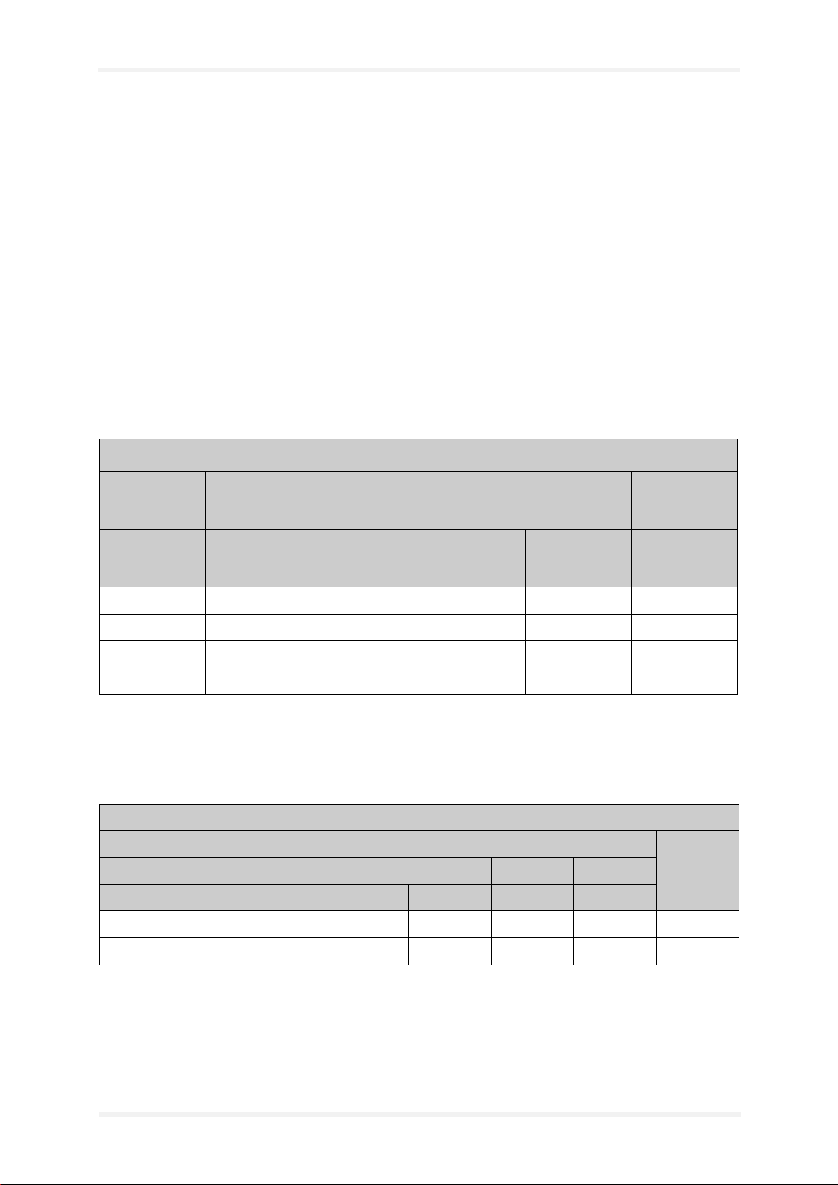
Signal acquisition performance
Initial ERROR uncertainties maximum
ephemeris
age
Satellite
acquisition state
Warm 0,40 100 75 5 4
Initialised 1,00 100 75 5 4
Cold 2,30 N/A* N/A N/A N/A
Frozen N/A N/A N/A N/A N/A
Table 15: Signal acquisition performance
TTFF 90 %
probable
(minutes)
position (km) velocity (m/sec) time (min.) hours
* Signal acquisition performance N/A = Not available
Accuracy
Position (meter) velocity
horizontal 3-D vertical
(meter/sec)
CEP (2 dRMS)
SA off 255093780.1
SA on 50 100 (95 %) 200 (95 %) 173 (95 %)
Table 16: Accuracy
A2D–JP Version 1.03 Side 22
Page 28
Description GPS receiver
6.2 Product overview
The GPS receiver requires conditioned 3,3 V DC power and a GPS
signal from a passive or active antenna.
The 12 channel architecture provides rapid Time-To-First-Fix
(TTFF) under all start-up conditions. As long as visible satellites are
not obscured, acquisition is guaranteed under all initialisation conditions.
To minimise TTFF when main power is removed from the GPS receiver SRAM with external DC supply voltage and EEPROM are
used to archive RTC time and prior position data.
Communication with the GPS receiver is established through two
asynchronous serial I/O ports. The GPS receiver's primary serial
port outputs navigation data and accepts commands from OEM application in NMEA-0183 format or CONEXANT binary format.
The secondary port is configured to accept differential GPS (DGPS)
corrections in the RTCM SC-104 format.
6.2.1 GPS receiver architecture
Figure 7: GPS receiver architecture
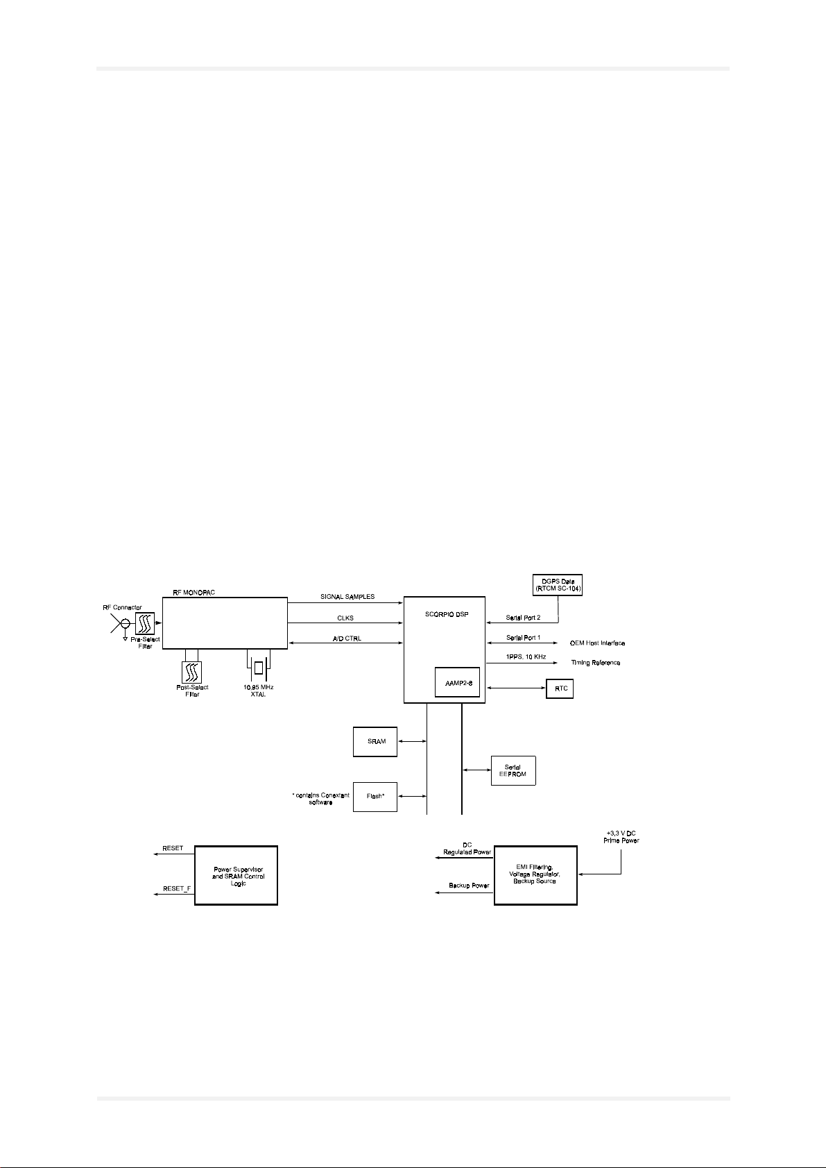
The functional architecture of the GPS receiver is shown in Figure 7.
The GPS receiver design is based on the Conexant Zodiac chip set,
the RF-Monopac and the Scorpio DSP, which contain the required
GPS functionality. The RF-Monopac contains all the RF down-conversion and amplification circuitry, and presents the In-Phase (I) and
Quadrature-Phase (Q) Intermediate.
A2D–JP Version 1.03 Side 23
Page 29

Description GPS receiver
Frequency (IF) sampled data to the Scorpio device. The Scorpio device contains an integral microprocessor and all the required GPSspecific signal processing hardware. Memory and other external
supporting components configure the GPS receiver into a complete
navigation system.
6.2.2 Product applications
Automotive applications
❐
Marine navigation applications
❐
Aviation applications
❐
Timing applications
❐
6.3 Technical description
6.3.1 General information
Since the GPS receiver determines its position by ranging signals
from four or more GPS satellites orbiting the Earth, its antenna must
have reasonable visibility of the sky.
Navigation modes
The GPS receiver supports three types of navigation mode operations.
Three dimensional navigation (3D): The GPS receiver
❐
defaults to 3-D navigation whenever at least four GPS satellites are being tracked In 3-D navigation, the GPS receiver computes latitude, longitude, altitude and time information from
satellites measurements.
Two dimension navigation (2D): When less than four GPS
❐
satellite signals are available or when a fixed value of altitude
can be used to produce an acceptable navigation solution, the
GPS receiver will enter the 2-D navigation mode. Forced operating in 2-D mode can be commanded by the OEM.
DGPS navigation: The GPS receiver processes DGPS cor-
❐
rections through its Auxiliary serial port. These corrections
must be compliant with the RTCM recommended standards
RTMC-104.
Satellites acquisition
The TTFF of the GPS receiver depends from start conditions.
Start condition means if old satellites data are available and how old
they are. The conditions are:
Warm start: results from an short (few minutes) interrupt by
❐
continuous navigation. Data are available in SRAM.
A2D–JP Version 1.03 Side 24
Page 30

Description GPS receiver
❐ Initialised start: is if last known position (in EEPROM) and
time are available. Satellite data validity has expired.
Cold start: means only almanac information is used.
❐
❐ Frozen start: no valid internal data source available.
Built in test (BIT) mode
A BIT is available on command from the application software using
binary Message 1300. The BIT is used to provide a health status of
the GPS receiver functions. Results of the BIT are available in binary
Message 1100. A BIT command is possible in NMEA protocol, too.
Power modes and power sequencing requirements
The GPS receiver have three power modes: Off, Operate, and
„Keep-Alive“.
The Off mode assumes that neither main power is available.
In the Operate mode the GPS receiver's components are full supplied at 3,3 VDC. The M_RST control signal is at a "high" logic level.
From Operate mode, the GPS receiver will enter a "Keep Alive"
mode when supply voltage is available at the VBATT signal input
and VC3 voltage is removed. VBATT provides power for SRAM and
RTC.
6.3.2 Hardware interface
The following paragraphs describe the basic functions allocated to
the various pins on the AMP interface connector. These functions
are divided into three groups: Configuration and timing signals, serial communication signals, and DC input signals.
6.3.2.1 Configuration and timing signals
Pin 55: Master reset (M_RST)
This signal allows the OEM to generate a system hardware reset to
the GPS receiver. This signal is capable of being driven directly by
an external microprocessor or by external logic without the need for
any external pull-up or pull-down resistors. The OEM can generate a
system reset to the GPS receiver by pulling the M_RST control signal low to ground.
The M_RST signal must be pulled to a CMOS logic „high“ level coincident
with, or after, the application of prime DC power for the receiver to enter its
Operate mode. The M_RST must be held at ground level for a minimum of
150 nanoseconds to assure proper generation of a hardware reset to the
receiver.
This signal can also be used to provide control of the GPS receiver's
Operate mode without removing prime input power from the GPS receiver. When M_RST is pulled to ground, the GPS receiver will enter
a low power state for as long as the M_RST signal is asserted low.
A2D–JP Version 1.03 Side 25
Page 31

Description GPS receiver
In this state, a portion of the GPS receiver's RF circuitry is de-energized, the SRAMs are transitioned into their low power data retention state, and the RTC device is maintained. When the GPS receiver is placed into this low power state through the use of the M_RST
control signal, the GPS receiver will continue to draw current from
the primary input power (PWRIN) but at a reduced level.
When the M_RST signal is subsequently asserted high by the OEM,
RF power is re-applied, a system reset is generated, and the GPS
receiver will return to its normal Operate mode.
Pins 56, 53, 54 and 51: General Purpose I/O (GPIO1, GPIO2,
GPIO3 and GPIO4)
The GPS receiver provides four General Purpose Input/Output
(GPIO) connections that are available for use by the OEM.
These GPIO connections are digital interfaces that are OEM software programmable as inputs or outputs.
Pin 41: UTC Time Mark Pulse (TMARK)
The Time Mark output provides a one pulse-per-second (1 pps)
signal to the OEM application processor. When the GPS receiver
provides a valid navigation solution, the rising edge of each TMARK
pulse is synchronized with the UTC one second epochs to within
±300 nsec.
Pin 42: 10 kHz UTC synchronized clock
This is a 10 kHz clock waveform that is synchronized to the UTC
TMARK pulse.
This clock signal is a positive logic, buffered CMOS level output.
6.3.3 Serial communication signals
Both the configuration and timing signals, described in the previous section,
and the serial communication signals described below must be applied
according to the limits shown in table 17.
Symbol Parameter Limits (*) Units
PWRIN 3 Main power input to the JP2 (+3,3 V DC) 3,135 to 3,465 volts
VIH (min) Minimum high-level input voltage 0.7 x PWRIN volts
VIH (max) Maximum high-level input voltage PWRIN volts
VIL (min) Minimum low-level input voltage - 0,3 volts
VIL (max) Maximum low-level input voltage 0,3 x PWRIN volts
VOH (min) Minimum high-level output voltage 0,8 x PWRIN volts
VOH (max) Maximum high-level output voltage PWRIN volts
Table 17: Digital signal requirements
A2D–JP Version 1.03 Side 26
Page 32

Description GPS receiver
Symbol Parameter Limits (*) Units
VOL (min) Minimum low-level output voltage 0 volts
VOL (max) Maximum low-level output voltage 0,2 x PWRIN volts
tr, tf Input rise and fall time 50 nanoseconds
C out Maximum output load capacitance 25 picofarads
(*) PWRIN refers to a + 3,3 V DC power input (PWRIN-3)
Table 17: Digital signal requirements
Pins 49 and 50: host port serial data input and output (SDO1
and SDI1)
The host port consists of a full-duplex asynchronous serial data interface. Both binary and NMEA initialization and configuration data
messages are transmitted and received across this port.
The default ROM settings for the host serial data port are binary
message format, 9600 baud, no parity, 8 data bits, and 1 stop bit.
The default may be modified using custom OEM software.
The serial port settings may also be changed to a new configuration
using binary serial message 1330. The new serial port settings are
stored in SRAM and serial EEPROM. The next time the GPS receiver is powered on or a master reset is initiated, the serial port configuration parameters are accessed in the following priority:
1. If SRAM checksums are valid, the communication parameters
and initialization data parameters will be read from SRAM.
2. If SRAM checksums are invalid and EEPROM checksums are
valid, the communication parameters and initialization data
parameters will be read from EEPROM.
3. If SRAM checksums are invalid and EEPROM checksums are
invalid, the default values in ROM will be used.
The OEM application must provide any Line Driver/Line Receiver
(LD/LR) circuitry to extend the range of the interface.
Port Idle is nominally a CMOS logical high (+ 3,3 V DC).
Pin 45 and 48: Auxiliary port serial data (SDI2 and SDO2)
The auxiliary port consists of a second half-duplex asynchronous
serial data interface. This port is configured to receive RTCM DGPS
correction data messages.
The default ROM settings for the Auxiliary Serial Data Port are 9600
baud, no parity, 8 data bits, and 1 stop bit. The default may be modified using custom OEM software.
The serial port settings may also be changed to a new configuration
using binary serial message 1330. The new serial port settings are
stored in SRAM and serial EEPROM. The next time the GPS receiver is powered on or a master reset is initiated, the serial port configuration parameters are accessed in the following priority:
1. If SRAM checksums are valid, the communication parameters
and initialization data parameters will be read from SRAM.
A2D–JP Version 1.03 Side 27
Page 33

Description GPS receiver
2. If SRAM checksums are invalid and EEPROM checksums are
valid, the communication parameters and initialization data
parameters will be read from EEPROM.
3. If SRAM checksums are invalid and EEPROM checksums are
invalid, the default values in ROM will be used.
The OEM application must provide any LD/LR circuitry to extend the
range of the interface. Port Idle is nominally a CMOS logical high
(+ 3,3 V DC).
6.3.4 DC input signals
Do not apply power to a passive antenna or damage to the receiver will occur.
!
Pin 59: Preamp power input (PREAMP)
The OEM may optionally supply power to a preamplifier using the
antenna cable center conductor. The maximum voltage is +12 V DC
and the current must not exceed 100 mA.
Pins 58 and 60: Power input (PWRIN 3)
This signal is the main power input to the GPS receiver.
Regulated DC power requirements are shown in table 2.
Pin 57: Battery backup power input (VBATT)
This signal is used to provide a DC power input to the SRAM and
RTC devices only. The GPS receiver automatically switches to the
VBATT input signal when primary DC power (PWRIN) is removed
from the board.
This feature is intended to provide the GPS receiver with a "warm
start" capability by maintaining an accurate time source and using
position and satellite data stored in SRAM after prime input power
(PWRIN) has been removed from the GPS receiver.
Pins 43, 44, 46, 47 and 52: Ground (GND)
DC grounds for the board. All grounds are tied together through the
GPS receiver's printed wiring board (PWB) ground plane and should
all be grounded externally to the GPS receiver.
6.3.5 Software interface
The host serial I/O port of the GPS receiver serial data interface supports full duplex communication between the GPS receiver and the
OEM application. Data messages can be in the Conexant binary format or NMEA-01 83 format. The GPS receiver also contains an
auxiliary port dedicated to direct processing of the RTCM SC-104
messages for DGPS corrections.
A2D–JP Version 1.03 Side 28
Page 34

Description GPS receiver
6.3.5.1 Binary data message
If you wish to use binary data message you get detailed information
in [6]. Binary data have more information but are difficult to use.
Output message name Default messages Message ID
Geodetic position status Position, ground speed, course over ground, climb
rate, map, datum and validity
Channel summary Signal tracking information per satellite 1002
Visible satellites Their corresponding elevation and azimuth best
possible DOP
Differential GPS status Corrections status of satellite 1005
Channel measurement 1007
ECEF position Per channel 1009
Receiver ID Send by power up 1011
User-settings 1012
Built in test results For the hardware parts 1100
UTC time mark pulse 110 8
Frequency standard Parameter in use 1110
Power management Duty cycle in use 1117
Serial port communication Parameters in use 1130
EEPROM update Show data ID for the last write 1135
EEPROM status Show failure and status information 1136
1000
1003
Frequency standard table 116 0
Boot status 118 0
Status/Error By firmware 1190
Geodetic position and velocity initialisation
User defined datum definition To transform the position solution 1210
Map datum select For 1210 1211
Satellite elevation mask control Set the elevation mask angle 1212
Satellites candidate select 1213
Differential GPS control 1214
Cold start control Disable cold start 1216
Solution validity criteria Position validity status 1217
User entered altitude input Define altitude for 2D navigation 1219
Application platform control Means special using 1220
Nav configuration Control features by navigation 1221
Table 18: Binary data message
Position, ground speed, course, over ground, climb
rate
1200
A2D–JP Version 1.03 Side 29
Page 35

Description GPS receiver
Output message name Default messages Message ID
Perform built in test 1300
Restart command With different start condition 1303
Frequency standard Input parameters
Power management control 1317
Serial port communication parameter
Message protocol control 1331
Factory calibration input For oscillator 1350
Raw DGPS RTCM SC-104 data In lieu of the auxiliary port 1351
Frequency standard table input data 1360
Flash reprogram For flash update 1380
Table 18: Binary data message
Is used by GPS without non-volatile storage 1310
1330
A2D–JP Version 1.03 Side 30
Page 36

Description GPS receiver
6.3.5.2 NMEA data message
Detailed information shown in [6].
Output message name Default messages Message ID
Conexant proprietary
Built In test
Conexant proprietary
Error/status
GPS Fix Data Time, position, HDOP GGA
GPS DOP and active satellites Operating mode, DOP per coordinate, satellite
GPS satellites in view Position an SNR per satellite. Max four satellites
Conexant proprietary
Receiver ID
Recommended minimum specific
GPS Data (*)
Track made good and ground Speed Course and speed VTG
Conexant proprietary
Zodiac channel status (*)
Input message name Default messages Message ID
Conexant proprietary built in test
command
Test results for devices BIT
ERR
GSA
number
GSV
per sentence
Channels, software version RID
Time, date, position, course and speed RMC
PRN, status ZCH
IBIT
Conexant proprietary log control
message
Conexant proprietary receiver
initialisation
Conexant proprietary
protocol message
Standard query message Request a NMEA message Q
Table 19: NMEA data message
Controls the output of the NMEA messages ILOG
Initialisation with specified parameters INIT
Set the message format to BIN IPRO
A2D–JP Version 1.03 Side 31
Page 37
Description A2D-JP evaluation board
7 A2D-JP evaluation board
The quickest way to get first results with the embedded GSM/GPS
module is the activation by the A2D-JP evaluation board by means
of a terminal program.
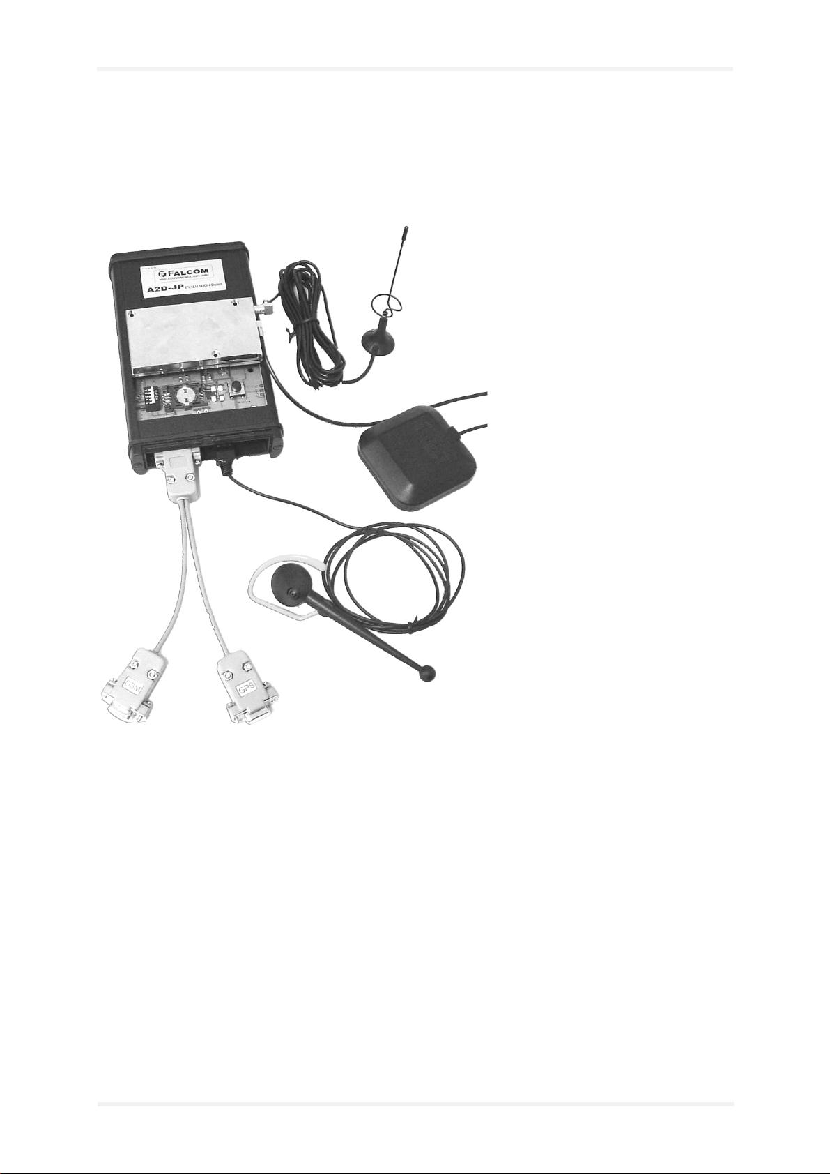
Figure 8: The A2D-JP evaluation board
Figure 8 shows the A2D-JP evaluation board in complete packaging
i. e.
– A2D-JP evaluation board
– A2D-JP module
– power supply FRIWO type FW 3299 (12 VDC/580 mA)
– GPS antenna ANT-006
– RS232 combined cable KA08
– headset with RJ45 plug
The evaluation board transfers data from GSM module and GPS receiver to two separate serial RS232 interfaces.
For voice communication by the GSM module there is a headset
A2D–JP Version 1.03 Side 32
Page 38

Description A2D-JP evaluation board
available.
So the data of both modules can be processed by your PC at the
same time.
Thus the evaluation board offers an excellent possibility for development and testing (trials) of your own application on the base of the
embedded GSM/GPS modules A2D-JP.
A2D–JP Version 1.03 Side 33
 Loading...