www.fairchildsemi.com
REV. 1.0.0 2/4/03
Features
• Very high performance, low cost
• Adaptive comb-based decoding
• Multiple pin-compatible versions
- 3-line, 2-line, and band-split
- 8- and 10-bit processing
• Internal digital linestores
• Supports NTSC/PAL field and NTSC frame based
decoding
• Multiple input formats
- CCIR-601/624 (D1), D2, CVBS, YC
• Multiple output formats
- CCIR-601/624 (D1), RGB, YC
BCR
• 10-18 Mpps data rate
• Parallel and serial control interface
• Single +5V power supply
Applications
• Studio television equipment
• Personal computer video input
• MPEG and JPEG compression inputs
Description
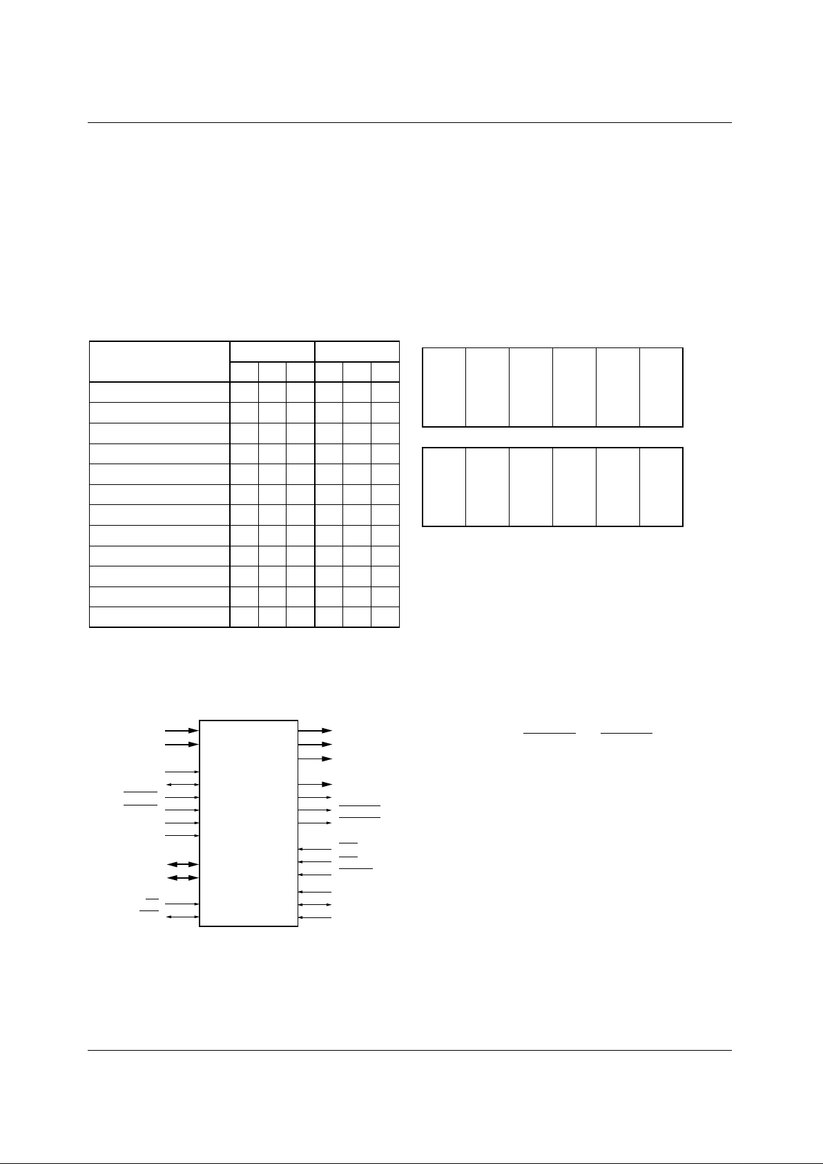
The TMC22x5yA family of Digital Video Decoders offers
unprecedented, broadcast-quality video processing performance in a single chip. It accepts line-locked or subcarrierlocked composite, YC, or D1 digital video and produces digital components in a variety of formats.
An internal three-line adaptive comb decoder structure produces optimal picture quality with a wide range of source
material. NTSC/PAL field and NTSC frame based decoding
is supported with external memory. Full comb programmability allows the user to tailor the decoder’s response to a
particular systems goals.
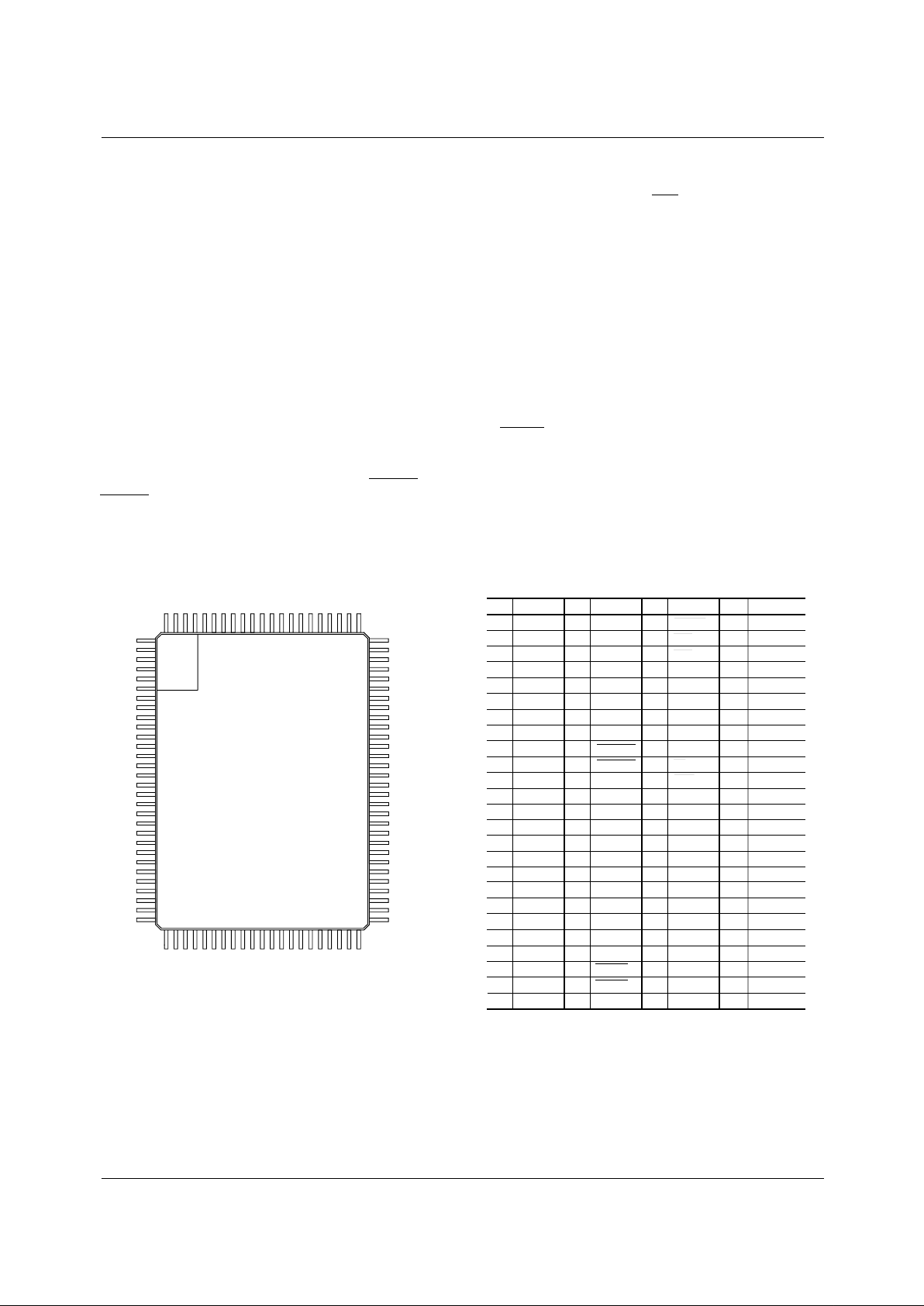
A family of products offers 3-line, 2-line, and simple decoders in 8-bit and 10-bit versions—all in a pin and softwarecompatible format. Serial and parallel control ports are provided. These submicron CMOS devices are packaged in a
100-lead Metric Quad Flat Pack (MQFP).
Related Products
• TMC22071 Genlocking Video Digitizer
• TMC22x9x 8 bit Digital Video Encoders
• TMC2081 Digital Video Mixer
• TMC3003 Triple 10-bit D/A Converter
• TMC1185 10 bit A/D converter
• TMC2192 10 bit video encoder
• TMC2072 Enhanced Genlocking Video Digitizer
Block Diagram
65-22x5y-01
Input
Processor
Output
Processor
Adaptive
Comb
Filter
VIDEOA
9-0
VIDEOB
9-0
G/Y
9-0
MASTER
1-0
BUFFER
CLOCK
HSYNC
VSYNC
LDV
DHSYNC
DVSYNC
DREF
FID
2-0
B/Cb
9-0
R/Cr
9-0
SER
A
1-0
SA
2-0
RESETSET
R/W SDACS SCL
D
7-0
Parallel Control Serial Control
Global Control
Internal
Sync Pulse
Generator
Y/C Split0
Y/C Split1
Linestore1
Linestore2
Y/C Split2
Chroma
Demod
Comb
Fail
Burst
Locked
Loop
TMC22x5yA
Multistandard Digital Video Decoder
Three-Line Adaptive Comb Decoder Family, 8 & 10 bit

TMC22x5yA PRODUCT SPECIFICATION
2 REV. 1.0.0 2/4/03
Table of Contents
Features......................................................................1
Applications ...............................................................1
Description .................................................................1
Block Diagram............................................................1
Contents .....................................................................2
List of Tables and Figures ........................................3
General Description...................................................4
Input Processor...............................................................4
Adaptive Comb Filter.....................................................4
Output Processor............................................................5
Parallel and Serial Microprocessor Interfaces................5
Pin Assignments........................................................5
Pin Descriptions.........................................................6
Control Register Map.................................................8
Control Register Definitions ...................................11
Decoder Introduction...............................................40
YC Separation..............................................................40
Comb Filter Architecture for YC Separation...............41
YC Line-Based Comb Filters.......................................42
D1 Line-Based Comb Filters .......................................42
NTSC Frame and Field Based Decoders ...............42
Composite Frame-Based Comb Filters........................42
Composite Field-Based Comb Filters..........................42
PAL Field Comb Decoders......................................42
Composite PAL Field Comb Filters.............................42
The TMC22x5yA Comb Filter Architecture............43
TMC22x5yA Functional Description.......................44
Input Processor.............................................................44
Bandsplit Filter (BSF)..................................................44
Comb Filter Input.........................................................45
Adaptive Comb Filter...................................................47
Comb Fails................................................................49
Comb Fail Detection....................................................49
Generation of the Comb Fail Signals.....................50
Luma Error Signals......................................................50
Hue and Saturation Error Signals.................................50
Picture Correlation.......................................................50
Adapting the Comb Filter ............................................50
XLUT...........................................................................51
Digital Burst Locked Loop ..........................................53
Color Kill Counter .......................................................53
PAL Color Frame Bit...................................................55
Hue Control..................................................................55
System Monitoring of the Burst Loop Error................55
Clamp Circuit.............................................................. 55
Pedestal Removal ........................................................ 55
Clamp Generator ......................................................... 55
Luma Notch Filter ....................................................... 56
Matrix.......................................................................... 56
Programmable U Scalar............................................... 56
Programmable V Scalar............................................... 56
Programmable Y Scalar............................................... 56
Programmable MS Scalar............................................ 56
Fixed (B-Y) and (R-Y) Scalars ...................................56
Y Offset....................................................................... 57
Matrix Limiters............................................................ 57
Examples of Output Matrix Operation........................ 57
Simple Luma Color Correction................................... 58
C
BCR
MSB Inversion ................................................. 58
Output Rounding......................................................... 58
Output Formats............................................................ 58
Decimating CBCR Data............................................... 58
Multiplexed YCBCR Output (TRS Words Inserted)... 58
YC Outputs.................................................................. 58
The LDV Clock........................................................... 58
Sync Pulse Generator .............................................59
Internal Field and Line Numbering Scheme ............... 59
Timing Parameters ..................................................61
Subcarrier Programming ............................................. 61
Horizontal Timing....................................................... 61
Horizontal and Vertical Timing Parameters................ 61
Vertical Blanking ........................................................62
VINDO Operation....................................................... 65
Video Measurement.................................................65
Pixel Grab.................................................................... 65
Composite Line Grab .................................................. 67
Parallel Microprocessor Interface ...............................67
Serial Control Port (R-Bus)......................................... 68
Equivalent Circuits and Threshold Levels ............71
Absolute Maximum Ratings....................................72
Operating Conditions..............................................73
Electrical Characteristics........................................75
Switching Characteristics.......................................76
System Performance Characteristics....................76
Programming Examples..........................................77
Programming Worksheet........................................81
Related Products .....................................................82
Ordering Information...............................................84

PRODUCT SPECIFICATION TMC22x5yA
REV. 1.0.0 2/4/03 3
List of Tables and Figures
Table 1. TMC22x5yA Decoder Family................. 4
Table 2. Normalized Subcarrier Frequency
as a Function of Pixel Data Rates....... 45
Table 3. Comb Filter Architecture..................... 48
Table 4. Simple Example of an Adaptive
Comb Filter Architecture..................... 48
Table 5. Adaption Modes ...................................51
Table 6. XLUT Input Selection........................... 52
Table 7. XLUT Output Function......................... 52
Table 8. XLUT Special Function Definitions..... 52
Table 9. PAL-B,G,H,I Bruch
Blanking Sequence.............................. 53
Table 10. PAL-M Bruch Blanking Sequence ......54
Table 11. Blanking Level Selection..................... 55
Table 12. Adaptive Notch Threshold Control..... 55
Table 13. Matrix Limiters...................................... 57
Table 14. Output Format ......................................58
Table 15. NTSC Field and Line Numbering ........59
Table 16. PAL B,G,H,I Field and
Line Numbering.................................... 59
Table 17. PAL M Field and Line Numbering....... 59
Table 18. Vertical Blanking Period...................... 60
Table 19. Vertical Burst Blanking Period............ 60
Table 20. Table of Line Idents, LID[4:0].............. 60
Table 21. Timing Offsets...................................... 61
Table 22. PAL VINDO operation ..........................63
Table 23. Pixel Grab Control................................ 66
Table 24. Parallel Port Control............................. 67
Table 25. Serial Port Addresses.......................... 69
Figure 1. Logic Symbol.......................................... 4
Figure 2. Pixel Data Format................................... 4
Figure 3. Fundamental Decoder
Block Diagram...................................... 40
Figure 4. Comparison of the Frequency
Spectrum of NTSC and PAL
Composite Video Signals.................... 40
Figure 5. Examples of Notch and Bandpass
Filters..................................................... 41
Figure 6. ............................................................... 41
Figure 7. Chrominance Vector Rotation in
PAL and NTSC...................................... 42
Figure 8. Chrominance Vector Rotation Over
4 Fields in NTSC................................... 42
Figure 9. Chrominance Vector Rotation Over
4 Fields in PAL...................................... 42
Figure 10. TMC22x5yA Line Based Comb
Filter Architecture ................................43
Figure 11. Input Processor.................................... 44
Figure 12. Complementary Bandsplit Filter......... 44
Figure 13. Bandsplit Filter, Full Frequency
Response.............................................. 45
Figure 14. Bandsplit Filter, Passband
Response.............................................. 45
Figure 15. Block Diagram of Comb Filter Input... 46
Figure 16. Signal Flow Around the Adaptive
Comb Filter ...........................................47
Figure 17. Example of a Comb Fail Using a NTSC
Two Line Comb Filter........................... 49
Figure 18. Generation of Upper and Lower Comb
Fail Signals ...........................................50
Figure 19. Comb Filter Selection ..........................51
Figure 20. XLUT Input Selection ........................... 52
Figure 21. Block Diagram of Digital Burst
Locked Loop......................................... 53
Figure 22. Gaussian Low Pass Filters.................. 54
Figure 23. Gaussian LPF Passband Detail........... 54
Figure 24. Output Processor Block Diagram....... 55
Figure 25. Adaptive Notch Filters ......................... 56
Figure 26. Luminance Notch Filter .......................56
Figure 27. Horizontal Timing................................. 61
Figure 28. External HSYNC and VSYNC Timing
for Field 1(3, 5, or 7)............................. 62
Figure 29. NTSC Vertical Interval.......................... 62
Figure 30. PAL-B,G,H,I,N Vertical Interval............ 62
Figure 31. PAL-M Vertical Interval........................ 63
Figure 32. Pixel Grab Locations............................ 64
Figure 33. Relationship Between Pixel Count
and Pixel Grab Value............................ 65
Figure 34. Microprocessor Parallel Port –
Write Timing.......................................... 66
Figure 35. Microprocessor Parallel Port –
Read Timing.......................................... 68
Figure 36. Serial Port Read/Write Timing............. 69
Figure 37. Serial Interface –
Typical Byte Transfer........................... 70
Figure 38. Equivalent Digital Input Circuit........... 71
Figure 39. Equivalent Digital Output ....................71
Figure 40. Threshold Levels for Three-state........ 71
Figure 41. Input Timing Parameters ..................... 72
Figure 42. Functional Block Diagram of the
TMC22x5yA G/Y, B/U, and R/V Output
Stage...................................................... 73
Figure 43. Output Timing Parameters .................. 74
TMC22x5yA PRODUCT SPECIFICATION
4 REV. 1.0.0 2/4/03
General Description
The TMC22x5yA digital decoder can be used as a universal
input to digital video processing systems by decoding digital
composite video and transcoding digital component inputs
into a common data format.
The digital comb filter decoder implements one of sixteen
comb filter architectures to produce luminance and color difference component signals which are virtually free of the
cross-color and cross-luminance artifacts associated with
simple bandsplit filter decoders.
Table 1. TMC22x5yA Decoder Family
Because the cost/performance tradeoff varies among applications, the TMC22x5yA decoder has been developed as a
family of six parts. They are all assembled in the same
package, and fit the same footprint. The register maps are
identical.
Figure 1. Logic Symbol
The devices come in 8- and 10-bit resolution versions (see
Figure 2 for data alignment between 8- and 10-bit versions).
Within each resolution version there are three models, offering three-line adaptive comb filtering, two-line adaptive
comb filtering, and simple decoding. The TMC22153A
10-bit three-line comb filter can be programmed to emulate
any of the other parts. All prototyping can be performed with
this version to evaluate performance tradeoffs, and lowercost versions are easily substituted in production.
Input Processor
The digitized video and clocks provided to the decoder can
be either locked to the line frequency or the subcarrier frequency of the digitized waveform, providing broadcast quality decoding from the NTSC square pixel rate of 12.27 MHz
to the PAL four times subcarrier pixel rate of 17.73 MHz.
Figure 2. Pixel Data Format
Inputs containing embedded GRS (Fairchild Video Input
Processors), TRS words (D1 multiplexed component signals), and TRS-ID words (deserialized D2 signals) can be
used to lock the internal horizontal and vertical state
machines to the embedded information. If this information is
not provided, external horizontal and vertical syncs are
required for all line-locked input formats, and are optional
for NTSC inputs locked to four times the subcarrier (4*Fsc).
A simple sync separator is provided for digitized inputs
locked to the subcarrier frequency: the internal sync separator locks to the mid point of syncs during the vertical field
group, then flywheels during the active portion of the field.
For this reason, the DHSYNC and DVSYNC operations are
not guaranteed in subcarrier mode.
Adaptive Comb Filter
The line based adaptive comb filter in the TMC22x5yA adds
or subtracts the high frequency data from three adjacent field
lines to produce the average of the high frequency luminance
by canceling the chrominance signals, which in flat fields of
color are 180 degrees apart. Unfortunately flat fields of color
are rare and, when vertical transitions in the picture occur,
the output of the comb filter contains a mixture of both high
frequency luminance and chrominance, at which time the
comb fails. To avoid the comb filter artifacts that occur when
this happens, three sets of error signals are sent to a user-programmable lookup table, allowing the output of the comb filter to be mixed with the output of an internal bandsplit
decoder.
To produce these comb fail error signals, the video on each
of the inputs to the comb filter is passed through a simple
bandsplit decoder. The low-frequenc y portion of the signal is
TMC2215yA TMC2205yA
Function 321321
10-bit Data ✔✔✔
8-bit Data ✔✔✔✔✔✔
D1 Interface ✔✔✔✔✔✔
Line-Locked Mode ✔✔✔✔✔✔
fSC-Locked Mode ✔✔✔✔✔✔
Genlock Mode ✔✔✔✔✔✔
NTSC Frame Comb ✔✔
NTSC/PAL Field Comb ✔✔
3-Line Comb ✔✔
2-Line Comb ✔✔ ✔✔
Line Grab ✔✔ ✔✔
Pixel Grab ✔✔✔✔✔✔
65-22x5yA-02
VIDEOA
9-0
BUFFER
LDV
HSYNC
MASTER
TMC22x5yA
Multistandard
Digital
Video
Decoder
CLOCK
CS
VSYNC
R/W
D
7-0
A
1-0
VIDEOB
9-0
G/Y
9-0
B/C
B9-0
R/C
R9-0
FID
2-0
AVOUT
DHSYNC
DVSYNC
SER
SET
RESET
SA
2-0
SDA
SCL
MSB LSB
VA9
VB9
G/Y9
B/CB9
R/C
R9
VA8
VB8
G/Y8
B/C
B 8
R/C
R8
•••
VA2
VB2
G/Y2
B/CB2
R/C
R2
VA1
VB1
G/Y1
B/CB1
R/C
R1
VA0
VB0
G/Y0
B/CB0
R/C
R0
10 bit
VA9
VB9
G/Y9
B/CB9
R/C
R9
VA8
VB8
G/Y8
B/C
B 8
R/C
R8
•••
VA2
VB2
G/Y2
B/CB2
R/C
R2
N/C
N/C
N/C
N/C
N/C
N/C
N/C
N/C
N/C
N/C
8 bit
PRODUCT SPECIFICATION TMC22x5yA
REV. 1.0.0 2/4/03 5
assumed to be luminance and the high frequency portion is
processed as chrominance to find the magnitude and phase of
the chrominance vector. These three components are then
compared across the (0H & 1H) and (1H & 2H) taps of the
comb filter to produce the difference in luminance, chrominance magnitude, and chrominance phase. These differences
are then translated in the user-programmable lookup table to
produce the “K” signal which controls the complementary
mix between the output of the comb filter and the simple
bandsplit decoder. That is, the “K” signals controls how
much of the combed high frequency luminance signal is subtracted from the simple bandsplit chrominance for chroma
combs, or added to the low frequency output of the bandsplit
for luma comb filters.
Output Processor
The demodulated chrominance signal and the luminance
signal are passed through a programmable output matrix,
producing RGB, YUV, or YCBCR. When the clock is at
27MHz, a D1 signal can be produced on the R/V output with
the embedded TRS words fixed to the external HSYNC and
VSYNC timing.
Parallel and Serial Microprocessor Interfaces
The parallel microprocessor interface employs 12 pins, the
serial port uses 5. A single pin, SER
, selects between the two
interface modes.
In parallel interface mode, one address line is decoded for
access to the internal control register and its pointer.
Controls are reached by loading a desired address through
the 8-bit D
7-0
port, followed by the desired data (read or
write) for that address. The control register address pointer
auto-increments to address 3Fh and then remains there.
A 2-line serial interface may also be used for initialization
and control. The same set of registers accessed by the parallel port is available to the serial port. The device address in
the serial interface is selected via pins SA
2-0
.
The RESET pin sets all internal state machines to their initialized conditions and places the decoder in a power-down
mode. All register data are maintained while in power-down
mode.
Pin Assignments
G/Y
1
G/Y
0
LDV
GND
V
DD
B/Cb
9
B/Cb
8
B/Cb
7
B/Cb
6
B/Cb
5
B/Cb
4
B/Cb
3
B/Cb
2
B/Cb
1
B/Cb
0
GND
V
DD
R/Cr
9
R/Cr
8
R/Cr
7
R/Cr
6
R/Cr
5
R/Cr
4
R/Cr
3
R/Cr
2
1
2
3
4
5
6
7
8
9
10
11
12
13
14
15
16
17
18
19
20
21
22
23
24
25
R/Cr
1
R/Cr
0
GND
V
DD
DREF
FID
0
FID
1
FID
2
DHSYNC
DVSYNC
D
0
D
1
D
2
GND
V
DD
D
3
D
4
D
5
D
6
D
7
GND
V
DD
HSYNC
VSYNC
BUFFER
26
27
28
29
30
31
32
33
34
35
36
37
38
39
40
41
42
43
44
45
46
47
48
49
50
Pin Name Pin Name
RESET
SET
SER
SA
0
SA
1
SA
2
GND
SDA
SCL
CS
R/W
A
0
A
1
GND
V
DD
VIDEOB
0
VIDEOB
1
VIDEOB
2
VIDEOB
3
VIDEOB
4
VIDEOB
5
VIDEOB
6
VIDEOB
7
VIDEOB
8
VIDEOB
9
51
52
53
54
55
56
57
58
59
60
61
62
63
64
65
66
67
68
69
70
71
72
73
74
75
GND
VIDEOA
0
VIDEOA
1
VIDEOA
2
VIDEOA
3
VIDEOA
4
VIDEOA
5
VIDEOA
6
VIDEOA
7
VIDEOA
8
VIDEOA
9
MASTER
0
MASTER
1
CLOCK
GND
V
DD
GND
G/Y
9
G/Y
8
G/Y
7
G/Y
6
G/Y
5
G/Y
4
G/Y
3
G/Y
2
76
77
78
79
80
81
82
83
84
85
86
87
88
89
90
91
92
93
94
95
96
97
98
99
100
Pin Name Pin Name
1
30
65-22x5y-03
31 50
51
80
81100

TMC22x5yA PRODUCT SPECIFICATION
6 REV. 1.0.0 2/4/03
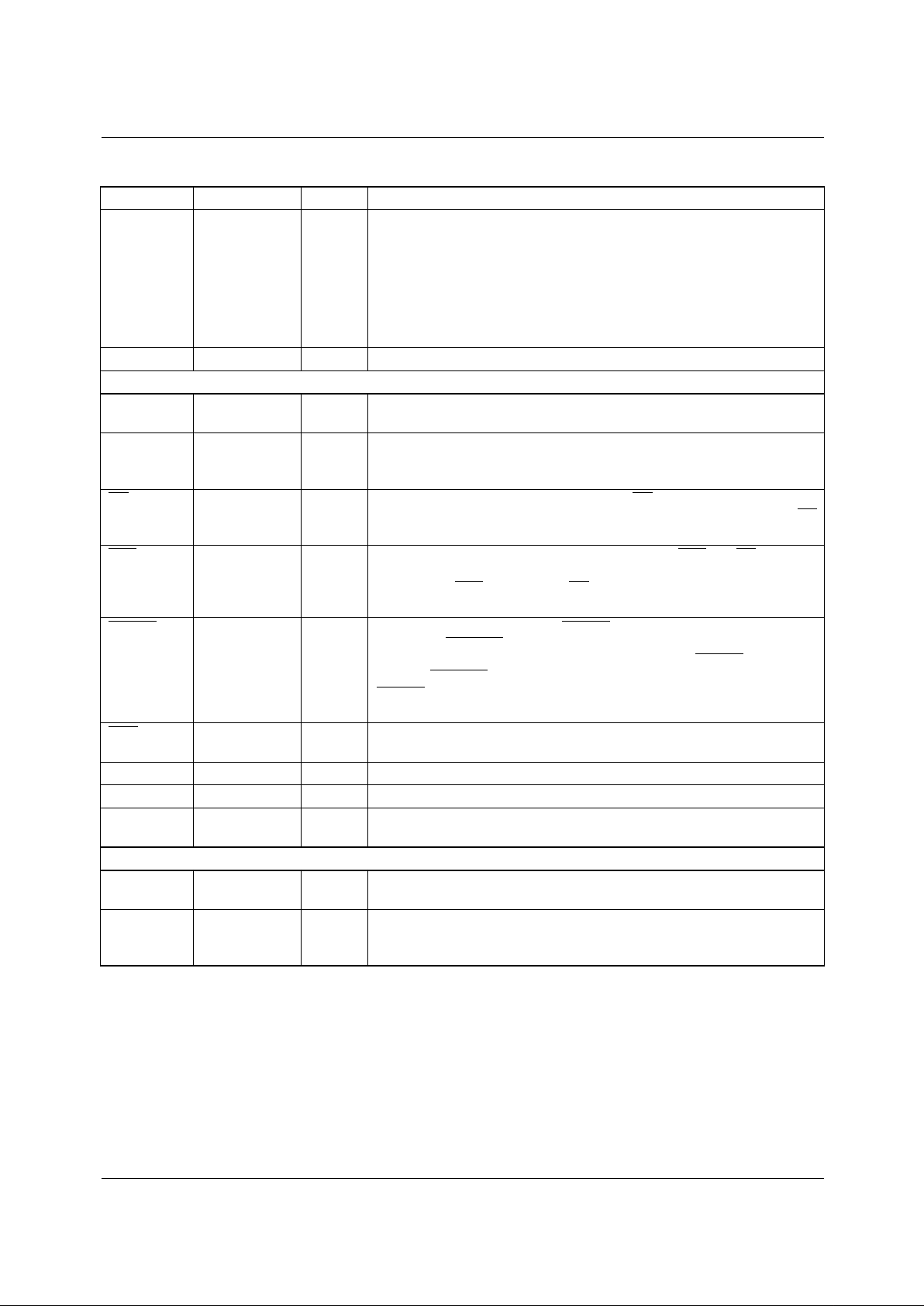
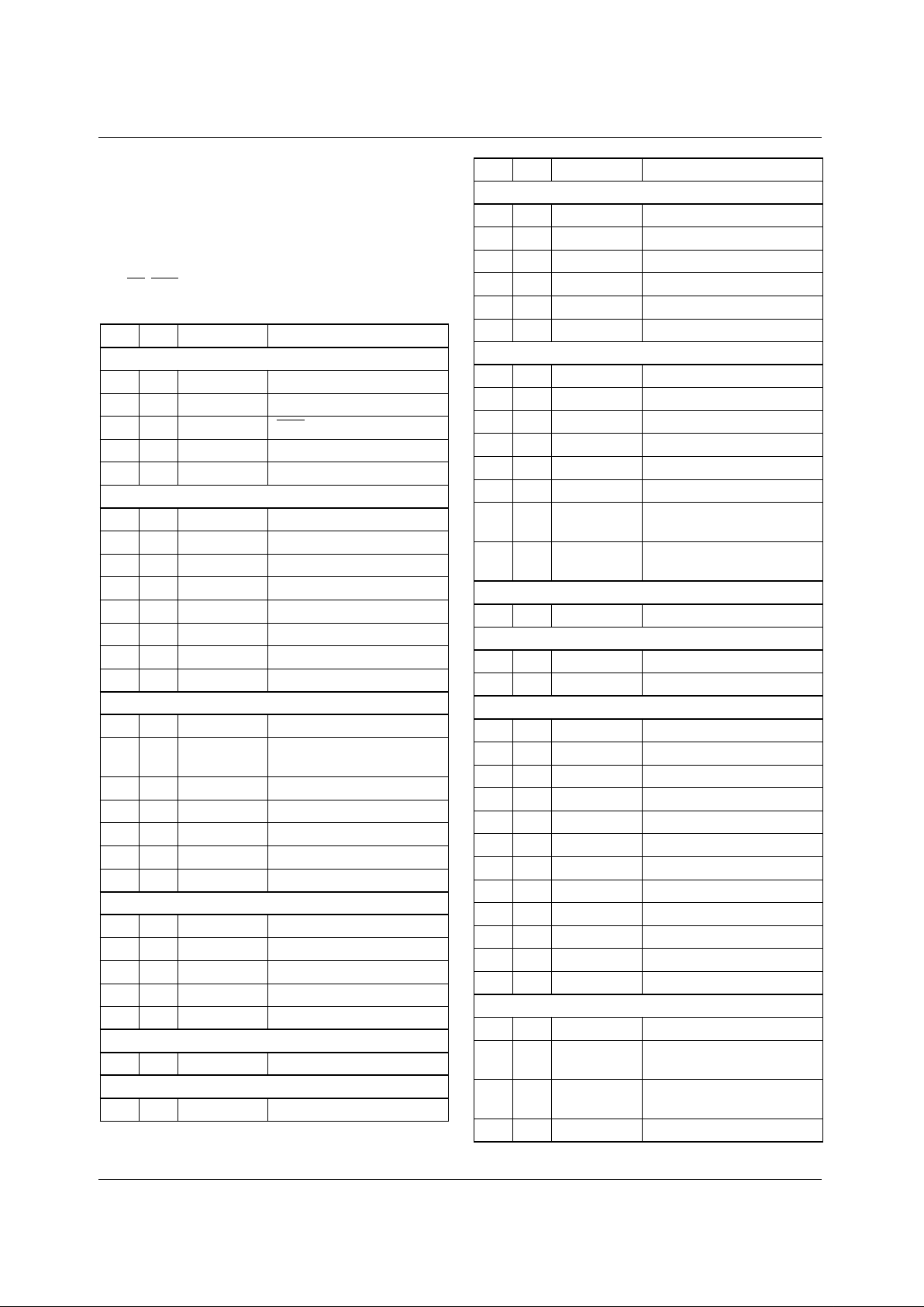
Pin Descriptions
Pin Name Pin Number Value Pin Function Description
Inputs
VIDEOA
9-0
86, 85, 84, 83,
82, 81, 80, 79,
78, 77
TTL Video input A. An 8 or 10 bit data input to the input multiplexer.
For 8-bit versions (TMC2205yA) the data are left-justified (VIDEOA
9-2
).
VIDEOB
9-0
75, 74, 73, 72,
71, 70, 69, 68,
67, 66
TTL Video input B. An 8 or 10 bit data input to the input multiplexer.
For 8-bit versions (TMC2205yA) the data are left-justified (VIDEOB
9-2
).
VSYNC 49 TTL Vertical sync input. A vertical sync signal (active low) occurring at the
start of the first vertical sync pulse in a vertical field group. A falling edge
of VSYNC
which is coincident with a falling edge of HSYNC indicates
field 1. This signal is active only when SPGIP
1-0
= 00.
HSYNC 48 TTL Horizontal sync input. A horizontal sync signal (active low) occurring
at the falling edge of the video sync. This signal is active only when
SPGIP
1-0
= 00.
MASTER
1-0
88, 87 TTL Master decoder control.
00 Adaptive comb decoder
01 Simple bandsplit decoder
10 Reserved
11 Flat notched luma and simple bandsplit chroma
BUFFER 50 TTL Control register select. This signal switches between two sets of
registers which control the gain or hue values in the output matrix.
When BUFFER = 0, registers 17-1F are active. When BUFFER = 1,
registers 27-2F take control.
CLOCK 89 TTL Master processing clock. The clock signal can either be at twice the
pixel data rate in the line locked modes, or at four times the subcarrier
frequency in the subcarrier mode. The interpretation of the CLOCK
signal is set by the CKSEL register bit.
SET 52 TTL Programmable function pin. The function specified by the SET
register is active when SET is low. The decoder returns to its previous
operation when SET goes high.
Outputs
G/Y
9-0
93, 94, 95, 96,
97, 98, 99, 100,
1, 2
TTL Green or Luminance digital output. For 8-bit versions (TMC2205yA)
the data are left-justified (G/Y
9-2
).
B/C
B9-0
6, 7, 8, 9, 10,
11, 12, 13, 14,
15
TTL Blue or CB digital output. For 8-bit versions (TMC2205y) the data are
left-justified (B/C
B 9-2
).
R/C
R9-0
18, 19, 20, 21,
22, 23, 24, 25,
26, 27
TTL Red or CR digital output. For 8-bit versions (TMC2205yA) the data are
left-justified (R/C
R 9-2
).
DVSYNC 35 TTL Vertical sync output. The DVSYNC signal occurs once per field and
lasts for 1 video line.
DHSYNC 34 TTL Horizontal sync output. The DHSYNC signal occurs once per line and
lasts for 64 clock periods.
LDV 3 TTL Data synchronization output. LDV can be an internally or externally
generated clock signal. The internal LDV signal is produced when the
CLOCK input is at twice the pixel data rate (PXCK); and is a pixel data
rate clock phase locked to the falling edge of the HSYNC. The external
LDV can be selected under software control, and must be at the
CLOCK, or a sub multiple of the CLOCK, frequency.
PRODUCT SPECIFICATION TMC22x5yA
REV. 1.0.0 2/4/03 7
DREF 30 TTL Decoder reference signal. This is a dual function pin, controlled by
register 24, that can function as an active video output indicator or
output as a clamp pulse. When set to the active video output function,
the DREF pin is HIGH during the video portion of each line and LOW
during the horizontal and vertical blanking levels. When set to output a
clamp pulse, the clamp pulse is controlled by register 24 and 25
allowing a user to program when a 0.5 µSec pulse is output relative to
HSYNC.
FID
2-0
33, 32, 31 TTL Field identification output. A 3 bit field ident from the DRS signal.
µP Interface
D
7-0
45, 44, 43, 42,
41, 38, 37, 36
TTL Parallel control port data I/O. All control parameters are loaded into
and read back over this 8 bit data port.
A
1-0
63, 62 TTL Parallel control port address inputs. These pins govern whether the
microprocessor interface selects a table/register address or reads/
writes table/register contents.
CS 60 TTL Parallel control port chip select. When CS is high the microprocessor
interface port, D
7-0
, is set to HIGH impedance and ignored. When CS
is LOW, the microprocessor can read or write parameters over D
7-0
.
R/W 61 TTL Parallel control port read/write control. When R/W and CS are LOW,
the microprocessor can write to the control registers or XLUT over
D
7-0
. When R/W is HIGH and CS is LOW, it can read the contents of
any selected XLUT address or control register over D
7-0
.
RESET 51 TTL Chip master reset. Bringing RESET LOW sets the software reset
control bit, SRESET, LOW and disables the digital outputs. If HRESET
is LOW the decoder outputs remain disabled after RESET goes HIGH
until the SRESET bit is set high by the host. If HRESET is HIGH when
RESET goes HIGH the decoder the internal state machines are
enabled.
SER 53 TTL Serial/parallel interface select. This pin will select between a parallel
(HIGH) or serial (LOW) interface port.
SDA 58 R-Bus Serial data interface. Bi-directional serial interface to the control port.
SCL 59 R-Bus Serial interface clock.
SA
2-0
56, 55, 54 TTL Serial Address. Three bits providing the lsbs of the serial chip ID used
to identify the decoder.
Power Supply
V
DD
5, 17, 29, 40,
47, 65, 91
+5 V Power Supply. Positive power supply for digital circuits, +5V.
GND 4, 16, 28, 39,
46, 57, 64, 76,
90, 92
0.0 V Ground. Ground for digital circuits, 0V.
Pin Descriptions (cont.)
Pin Name Pin Number Value Pin Function Description
TMC22x5yA PRODUCT SPECIFICATION
8 REV. 1.0.0 2/4/03
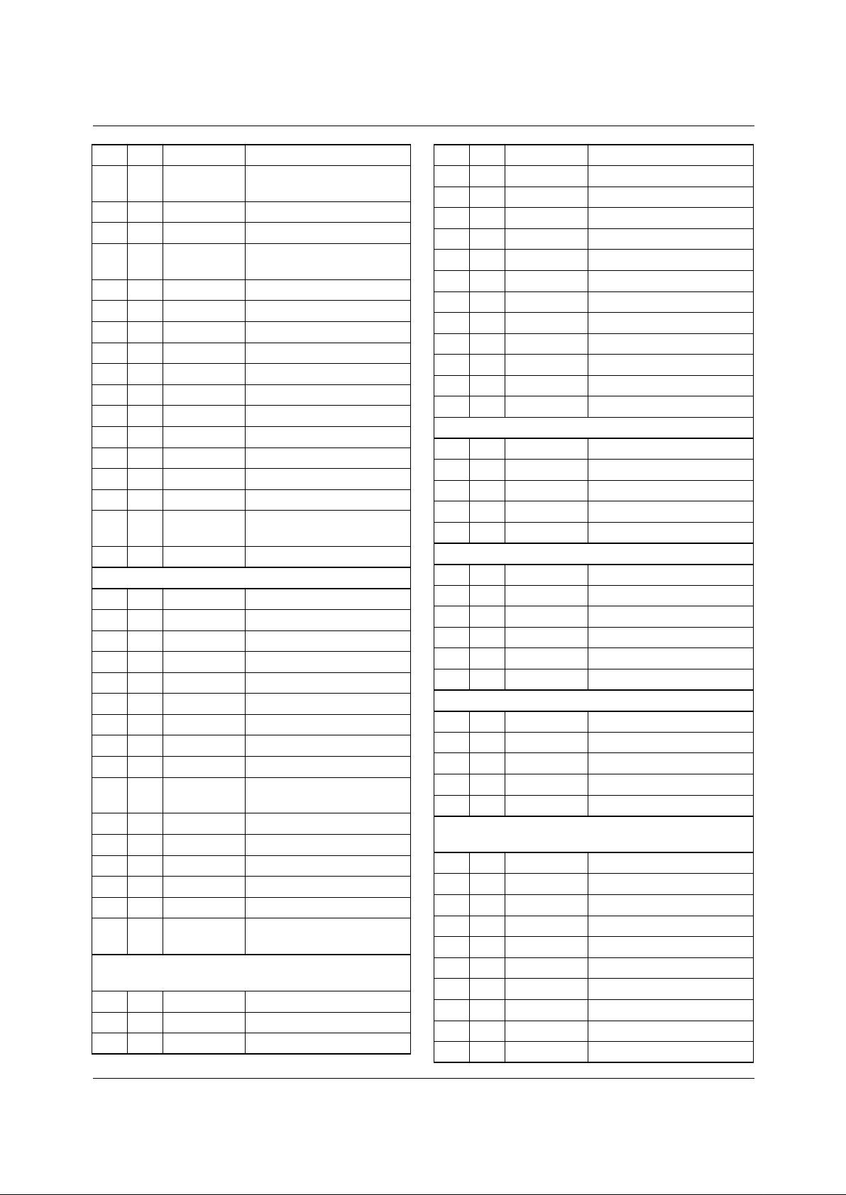
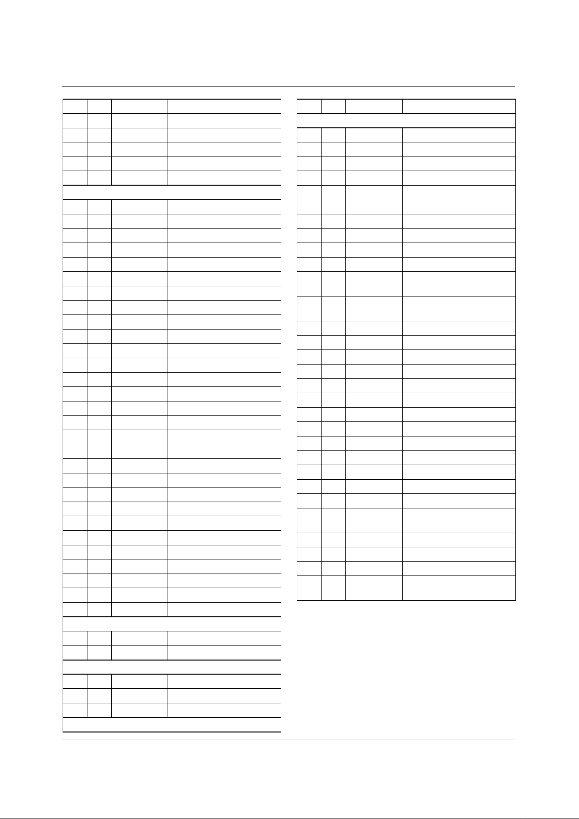
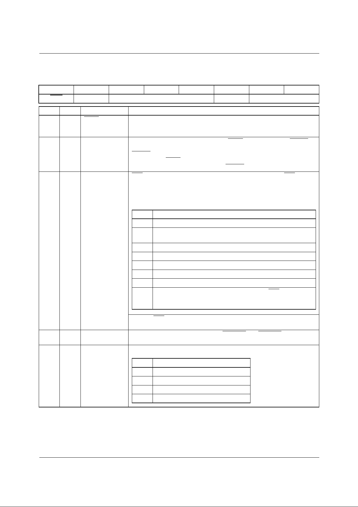
Control Register Map
The TMC22x5yA is initialized and controlled by a set of
registers which determine the operating modes.
An external controller is employed to write and read the
Control Registers through either the 8-bit parallel or 2-line
serial interface port. The parallel port, D
7-0
, is governed by
pins CS
, R/W , and A
1-0
. The serial port is controlled by SDA
and SCL.
Reg Bit Name Function
Global Control
00 7 SRST Software reset
00 6 HRST Hardware reset
00 5-3 SET SET
pin function
00 2 DHVEN Output H&V sync enable
00 1-0 STD Selects video standard
Input Processor Control
01 7 reserved, set to zero
01 6 IPMUX Input mux control
01 5 IP8B 8 bit input format
01 4 TDEN TRS detect enable
01 3 TBLK TRS blank enable
01 2 IPCMSB Chroma input msb invert
01 1 ABMUX AB mux control
01 0 CKSEL Input clock rate select
Burst Loop Control
02 7 BLLRST BLL auto. reset enable
02 6 VIPEN Video Input Processor
enable
02 5-4 LOCK Global lock mode
02 3 BLM BLL lock mode
02 2 KILD Color kill disable
02 1 DMODBY Demod bypass
02 0 CINT CBCR interpolation enable
Chroma Processor Control
03 7-5 BLFS Burst loop filter select
03 4 CCEN Chroma coring enable
03 3-2 CCOR Chroma coring threshold
03 1 GAUBY Gaussian filter bypass
03 0 GAUSEL Gaussian filter select
Burst Threshold
04 7-0 BTH Burst threshold
Pedestal
05 7-0 PED Pedestal level
Luma Processor Control
06 7-6 reserved, set to zero
06 5 ANEN Adaptive notch enable
06 4 ANR Adaptive notch rounding
06 3-2 ANT Adaptive notch threshold
06 1 ANSEL Adaptive notch select
06 0 NOTCH Notch enable
Comb Processor Control
07 7 LS1BY Line store 1 bypass
07 6 LS1IN Line store 1 input
07 5 LS2DLY Line store 2 delay
07 4 SPLIT Line store 2 data width
07 3 BSFBY Bandsplit filter bypass
07 2 BSFSEL Bandsplit filter select
07 1 BSFMSB Inverts msb of bandsplit
filter
07 0 GRSDLY Delays input to GRS
decode by 1H
Mid-Sync Level
08 7-0 MIDS Mid-sync level
Extended DRS
09 7-4 PCKF Clock rate
09 3-0 VSTD Video standard
Output Control
0A 7 OP8B Output rounded to 8 bits
0A 6-5 OPLMT Output limit select
0A 4-3 MSEN Mixed sync enable
0A 2 OPCMSB Chroma output msb invert
0A 1 YBAL Luma color correction
0A 0 BUREN Output burst enable
0B 7 FMT422 Enables C
BCR
output mux
0B 6 CDEC CBCR decimation enable
0B 5 YUVT Enables D1 output
0B 4-2 reserved, set to zero
0B 1 DRSEN DRS output enable
0B 0 DRSCK DRS data rate
Comb Filter Control
0C 7-6 ADAPT Adaption mode
0C 5 YCES YC input error signal
control
0C 4 YCSEL luma/chroma comb filter
select
0C 3-0 COMB Comb filter architecture
Reg Bit Name Function
PRODUCT SPECIFICATION TMC22x5yA
REV. 1.0.0 2/4/03 9
0D 7-6 CEST Chroma error signal
transform
0D 5 CESG Chroma error signal gain
0D 4 YESG Luma error signal gain
0D 3 CESTBY Chroma error signal
bypass
0D 2 XFEN XLUT filter enable
0D 1 FAST Adaption speed select
0D 0 YWBY Luma weighting bypass
0E 7-6 XIP XLUT input select
0E 5-4 XSF XLUT special function
0E 3-2 YMUX Y output select
0E 1-0 CMUX C output select
0F 7 reserved, set to zero
0F 6-5 CAT Adaption Threshold
0F 4 DCES D1 C
BCR
error signal
0F 3-2 IPCF Comb filter input select
0F 1 YCCOMP YC or Composite input
select
0F 0 SYNC Sync processor select
Sync Pulse Generator
10 7-0 STS
7-0
Sync to sync 8 lsbs
11 7-0 STB Sync to burst
12 7-0 BTV Burst to video
13 7-0 AV
7-0
Active video line 8 lsbs
14 7-6 reserved, set to zero
14 5-4 AV
9-8
Active video line 2 msbs
14 3 reserved, set to zero
14 2-0 STS
10-8
Sync to sync 3 msbs
15 7 reserved, set to zero
15 6-2 VINDO Number of lines in vertical
window
15 1 VDIV Action inside VINDO
15 0 VDOV Action outside VINDO
16 7-6 reserved, set to zero
16 5-4 NFDLY new field detect delay
16 3-2 SPGIP SPG input select
16 1-0 MSIP Mixed sync separator input
select
Buffered register set 0
Active when BUFFER pin set LOW
17 7-0 SG0
7-0
Msync gain, 8 lsbs
18 7-0 YG0
7-0
Y gain, 8 lsbs
19 7-0 UG0
7-0
U gain, 8 lsbs
Reg Bit Name Function
1A 7-0 VG0
7-0
V gain, 8 lsbs
1B 7-6 YG0
9-8
Y gain, 2 msbs
1B 5-3 UG0
10-8
U gain, 3 msbs
1B 2 reserved, set to zero
1B 1-0 VG0
9-8
V gain, 2 msbs
1C 7-0 YOFF0
7-0
Y offset, 8 lsbs
1D 7-3 reserved, set to zero
1D 2 YOFF0
8
Y offset, msb
1D 1-0 SG0
7-0
Msync gain, 2 msbs
1E 7-1 SYSPH0
6-0
7 lsbs of phase
1E 0 VAXISO V axis flip
1F 7-0 SYSPH0
14-7
8 msbs of phase
Normalized Subcarrier Frequency
20 7-4 FSC
3-0
Bottom 4 bits of f
SC
20 3-0 reserved, set to zero
21 7-0 FSC
11-4
Lower 8 bits of f
SC
22 7-0 FSC
19-12
Middle 8 bits of f
SC
23 7-0 FSC
27-20
Top 8 bits of f
SC
Clamp Control
24 7 DRFSEL Clamp pulse enable
24 6 PFLTBY Phase filter enable
24 5-4 CLPSEL
1-0
Int. clamp selection
24 3 VCLPEN Clamp bypass
24 2-0 BAND
2-0
Clamp offset
25 7-0 CPDLY
7-0
Clamp pulse delay
Output Format Control
26 7-6 reserved, set to zero
26 5 LDVIO LDV clock select
26 4 OPCKS Output clock select
26 3 DPCEN DPC enable
26 2-0 DPC Decoder product code
Buffered register set 1
Active when BUFFER pin set HIGH
27 7-0 SG1
7-0
Msync gain, 8 lsbs
28 7-0 YG1
7-0
Y gain, 8 lsbs
29 7-0 UG1
7-0
U gain, 8 lsbs
2A 7-0 VG1
7-0
V gain, 8 lsbs
2B 7-6 YG1
9-8
Y gain, 2 msbs
2B 5-3 UG1
10-8
U gain, 3 msbs
2B 2 reserved, set to zero
2B 1-0 VG1
9-8
V gain, 2 msbs
2C 7-0 YOFF1
7-0
Y offset, 8 lsbs
2D 7-3 reserved, set to zero
Reg Bit Name Function
TMC22x5yA PRODUCT SPECIFICATION
10 REV. 1.0.0 2/4/03
2D 2 YOFF1
8
Y offset, msb
2D 1-0 SG1
7-0
Msync gain, 2 msbs
2E 7-1 SYSPH1
6-0
7 lsbs of phase
2E 0 VAXIS1 V axis flip
2F 7-0 SYSPH1
14-7
8 msbs of phase
Video Measurement
30 7 set to zero
30 6 LGF Line grab flag
30 5 LGEN Line grab enable
30 4 LGEXT Ext line grab enable
30 3 reserved, set to zero
30 2 PGG Pixel grab gate
30 1 PGEN Pixel grab enable
30 0 PGEXT Ext pixel grab enable
31 7-0 PG
7-0
Pixel grab, 8 lsbs
32 7-0 LG
7-0
Line grab, 8 lsbs
33 7 reserved, set to zero
33 6-4 FG Field grab number
33 3 LG
8
Msb of line grab
33 2-0 PG
10-8
Pixel grab, 3 msbs
34 7-0 GY
9-2
G/Y grab, 8 msbs
35 7-0 BU
9-2
B/U grab, 8 msbs
36 7-0 RV
9-2
R/V grab, 8 msbs
37 7-6 reserved
37 5-4 GY
1-0
G/Y grab, 2 lsbs
37 3-2 BU
1-0
B/U grab, 2 lsbs
37 1-0 RV
1-0
R/V grab, 2 lsbs
38 7-0 Y
9-2
Luma grab, 8 msbs
39 7-0 M
9-2
Msync grab, 8 msbs
3A 7-0 U
9-2
U grab, 8 msbs
3B 7-0 V
9-2
V grab, 8 msbs
3C 7-6 Y
1-0
Luma grab, 2 lsbs
3C 5-4 M
1-0
Msync grab, 2 lsbs
3C 3-2 U
1-0
U grab, 2 lsbs
3C 1-0 V
1-0
V grab, 2 lsbs
Test Control
3D 7-0 TEST Must be set to zero
3E 7-0 TEST Must be set to zero
Vertical Blanking Control
3F 7 VBIT20 V bit control
3F 6 PEDDIS Pedestal control
3F 5-0 CCDEN
5-0
Closed caption control
Auto-increment stops at 3F
Reg Bit Name Function
Notes:
1. Functions are listed in the order of reading and writing.
2. For each register listed above up to register 3F, all bits not
specified are reserved and must be set to zero to ensure
proper operation.
Status - Read Only
40 7-0 DDSPH DDS phase, 8 msbs
41 7 LINEST Pixel count reset
41 6 BGST Start of burst gate
41 5 VACT2 Half line flag
41 4 PALODD PAL Ident
41 3 VFLY Vertical count reset
41 2 FGRAB Field grab
41 1 LGRAB Line grab
41 0 PGRAB Pixel grab
42 7 FLD Field flag (F in D1 output)
42 6 VBLK Vertical blanking (V in D1
output)
42 5 HBLK Horizontal blanking (H in
D1 output)
42 4-0 LID Line identification
43 7 YGO Y/G overflow
43 6 YGU Y/G underflow
43 5 UBO C
B
/B overflow
43 4 UBU CB/B underflow
43 3 VRO CR/R overflow
43 2 VRU CR/R underflow
43 1-0 reserved
44 7 MONO Color kill active
44 6-0 FPERR Frequency/Phase error
45 7-0 DRS DRS signal
46 7-0 PARTID Reads back xx
h
47 7-0 REVID Revision number
48-4A7-0 reserved
4B 7 PKILL Phase kill from comb fail
4B 6-5 CFSTAT Comb filter status
4B 4-0 XOP XLUT output
4C-FF7-0 reserved
Reg Bit Name Function
PRODUCT SPECIFICATION TMC22x5yA
REV. 1.0.0 2/4/03 11
Control Register Definitions
Global Control Register (00)
76543210
SRST
HRST SET DHVEN STD
Reg Bit Name Description
00 7 SRST Software reset. When LOW, resets and holds internal state machines and
disables outputs. When HIGH (normal), starts and runs state machines and
enables outputs. This bit is ignored while HRST is high.
00 6 HRST Hardware reset. When HRST is HIGH, SRST
is forced low when RESET pin
is taken LOW. State machines are reset and held. When HRST is low the
RESET
pin can be taken HIGH at any time. The state machines remain
disabled until SRST is programmed HIGH. When HRST is high the state
machines are enabled as soon as the RESET pin goes HIGH.
00 5-3 SET SET pin function. These bits control the set function when the SET pin goes
low.
A = all outputs high-impedance
B = internal state machines
C = burst locked loop
The first SET pulse after a software or hardware reset, with SET = 111,
causes a toggle to SET = 010.
00 2 DHVEN Output H&V sync enable. Disables DHSYNC and DVSYNC signals when
HIGH.
00 1-0 STD Selects video standard. Selects video standard.
SET Function
000 Reset and hold A, B, & C.
001 Set output to BLUE and flywheel B & C. (RGB outputs)
Set output to "color" and flywheel B & C (YCBCR outputs)
010 Hold A, lock B & C to external input
011 Reset C only
100 Reset B & C
101 Set output to BLUE and lock B & C to input video (RGB output)
110 Line and pixel grab depending on VMCR
6-0
(reg 30)
111 Toggle reset function of SET = 010. For each SET = 0 pulse the
chip operation will change from normal to that of SET = 010 or
visa versa.
SET Function
00 NTSC
01 reserved
10 PAL/M
11 All PAL standards except PAL/M

TMC22x5yA PRODUCT SPECIFICATION
12 REV. 1.0.0 2/4/03
Control Register Definitions (continued)
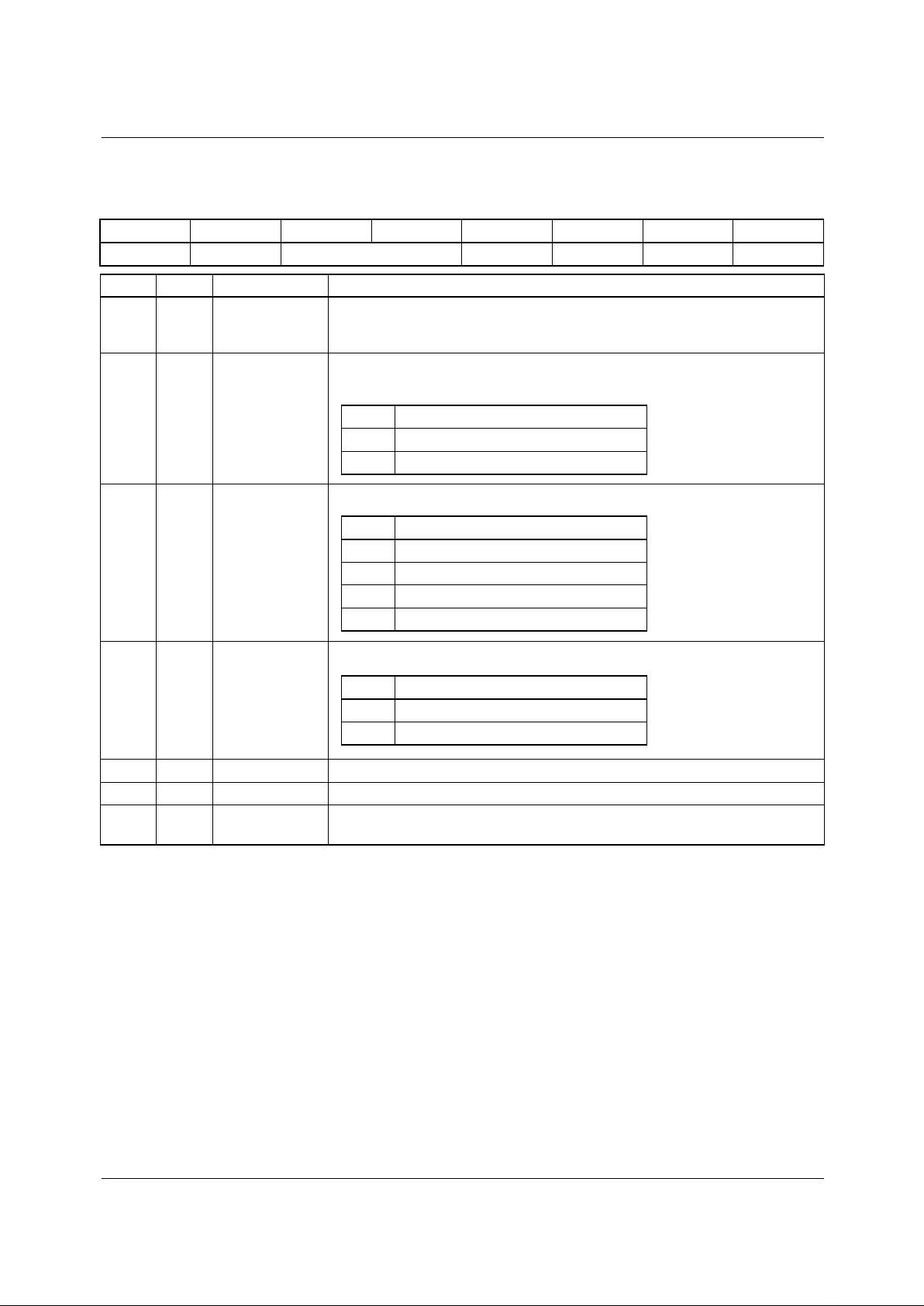
Input Processor Control (01)
76543210
Reserved IPMUX IP8B TDEN TBLK IPCMSB ABMUX CKSEL
Reg Bit Name Description
01 7 Reserved Reserved, set to zero.
01 6 IPMUX Input mux control. Used to select the Video Input Processor, D1, or D2 data
as the VA input to the input processor.
VIDEOA is selected for VA and VIDEOB is selected for VB when IPMUX is
set LOW. VIDEOB is selected for VA and VIDEOA for VB when IPMUX is set
HIGH. For YC inputs, the luma data must be passed through the VA input and
chroma through the VB input.
IPMUX should be set LOW for line locked composite inputs.
01 5 IP8B 8 bit input format. Bottom two bits of inputs VIDEOA
9-0
and VIDEOB
9-0
are
set to zero when HIGH.
01 4 TDEN TRS detect enable. When HIGH, the TRS words embedded in incoming
video are used to reset the horizontal and vertical state machines. When LOW
the externally provided or internally generated HSYNC and VSYNC are used
to reset the horizontal and vertical state machines.
01 3 TBLK TRS blank enable. Blanks the TRS and AUX data words when HIGH. For line
locked and D1 data, the TRS and AUX data words are set to the luma and
chroma blanking levels as appropriate. For D2 (4*fSC) data, the TRS and
AUX data words are set to the sync tip level.
01 2 IPCMSB Chroma input msb invert. The msb of the chroma or CBCR data are inverted
when HIGH.
01 1 ABMUX AB mux control. Selects the primary and secondary inputs to the decoder
from the DA and DB outputs of the input processor. When ABMUX is LOW,
DA is selected as the primary and DB as the secondary decoder input.
01 0 CKSEL Input clock rate select. Set HIGH for line locked clocks and LOW for
subcarrier locked clocks. Line locked clocks should be at twice the pixel data
rate, and the subcarrier clock should be at four times the subcarrier
frequency.
PRODUCT SPECIFICATION TMC22x5yA
REV. 1.0.0 2/4/03 13
Control Register Definitions (continued)
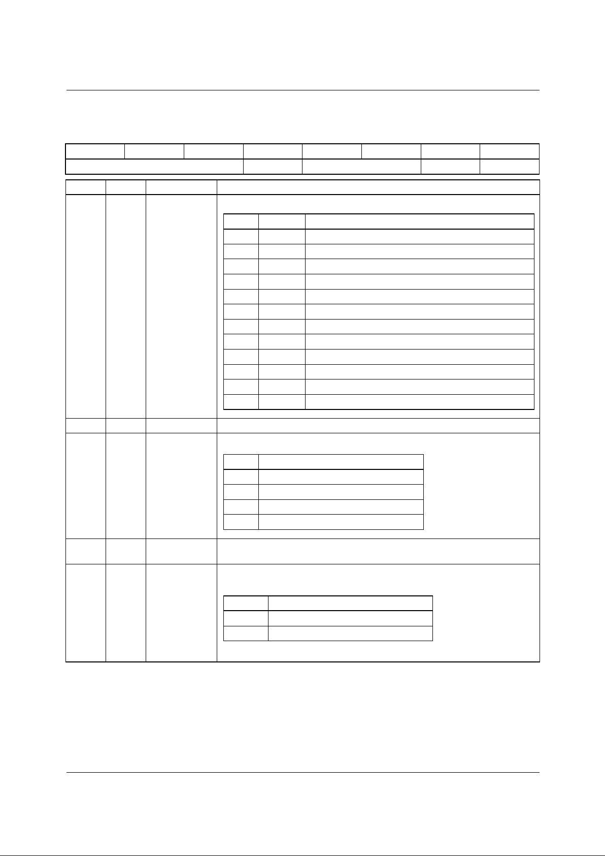
Burst Loop Control (02)
76543210
BLLRST VIPEN LOCK BLM KILD DMODBY CINT
Reg Bit Name Description
02 7 BLLRST BLL reset enable. When LOW, the automatic BLL reset is disabled. When
HIGH, the BLL will be reset if the BLL loses lock and fails to reacquire lock
within 8 fields.
02 6 VIPEN Video Input Processor enable. Selects interface protocol for Fairchild video
input devices. Active only when LOCK
1-0
= 10.
02 5-4 LOCK Global Lock mode. Sets the decoder locking mode.
02 3 BLM BLL lock mode. Sets the decoder burst locking mode.
02 2 KILD Color kill disable. Color killer is disabled when HIGH.
02 1 DMODBY Demod bypass. Chroma data bypasses the demodulator when HIGH.
02 0 CINT CBCR interpolation enable. Interpolation of CBCR input data from 0:2:2 to
0:4:4 is enabled when HIGH.
VIPEN Function
0 Video Input Processor Interface
1 TMC22071 Interface
LOCK Function
00 Line Locked Mode
01 Subcarrier Locked Mode
10 Video Input Processor Mode
11 D1 Mode
BLM Function
0 Frequency Lock
1 Phase Lock
TMC22x5yA PRODUCT SPECIFICATION
14 REV. 1.0.0 2/4/03
Control Register Definitions (continued)
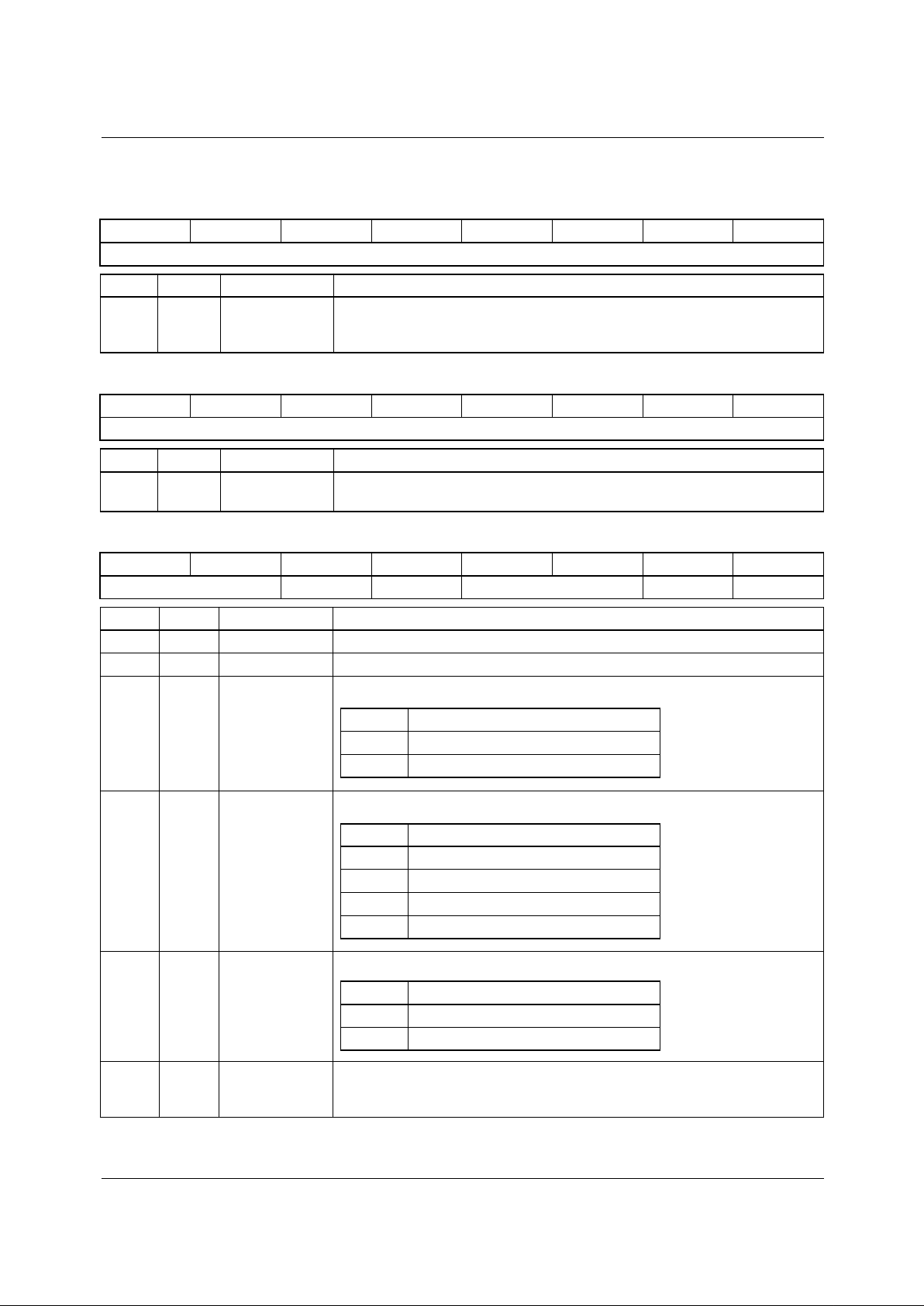
Chroma Processor Control (03)
76543210
BLFS CCEN CCOR GAUBY GAUSEL
Reg Bit Name Description
03 7-5 BLFS Burst loop filter select.
03 4 CCEN Chroma coring enable. Enables Chroma Coring when HIGH.
03 3-2 CCOR Chroma coring threshold. Sets the Chroma Coring threshold.
03 1 GAUBY Gaussian filter bypass. The chroma data bypasses the Gaussian LPF when
HIGH.
03 0 GAUSEL Gaussian LPF select. Selects the Gaussian filter response to be used on the
demodulated chrominance.
See Figure 22 for filter responses.
BLFS fS (Mpps) Recommended Criteria
000 13.5 PAL, Line-Locked YC
000 15 PAL, Line-Locked YC
001 12.27 NTSC, Line-Locked YC
001 13.5 PAL, Line-Locked Composite
010 13.5 NTSC, Line-Locked YC
010 15 PAL, Line-Locked Composite
011 14.32 NTSC, Subcarrier-Locked YC
011 17.73 PAL, Subcarrier-Locked Composite
100 17.73 PAL, Subcarrier-Locked YC
101 13.5 NTSC, Line-Locked Composite
110 12.27 NTSC, Line-Locked Composite
111 14.32 NTSC, Subcarrier-Locked Composite
CCOR Function
00 1 lsb
01 2 lsb
10 3 lsb
11 4 lsb
GAUSEL Function
0 Select Gaussian LPF resp. 2
1 Select Gaussian LPF resp. 1
PRODUCT SPECIFICATION TMC22x5yA
REV. 1.0.0 2/4/03 15
Control Register Definitions (continued)
Burst Threshold (04)
76543210
BTH
Reg Bit Name Description
04 7-0 BTH Burst threshold. The 8 bit value to be compared against the demodulated
U and V component data. If over 127 lines occur in a field in which the burst
is below this threshold, then the color is set to chroma black for the next field.
Pedestal (05)
76543210
PED
Reg Bit Name Description
05 7-0 PED Pedestal level. An 8 bit magnitude subtracted from the luma data to remove
the setup before processing by the output matrix.
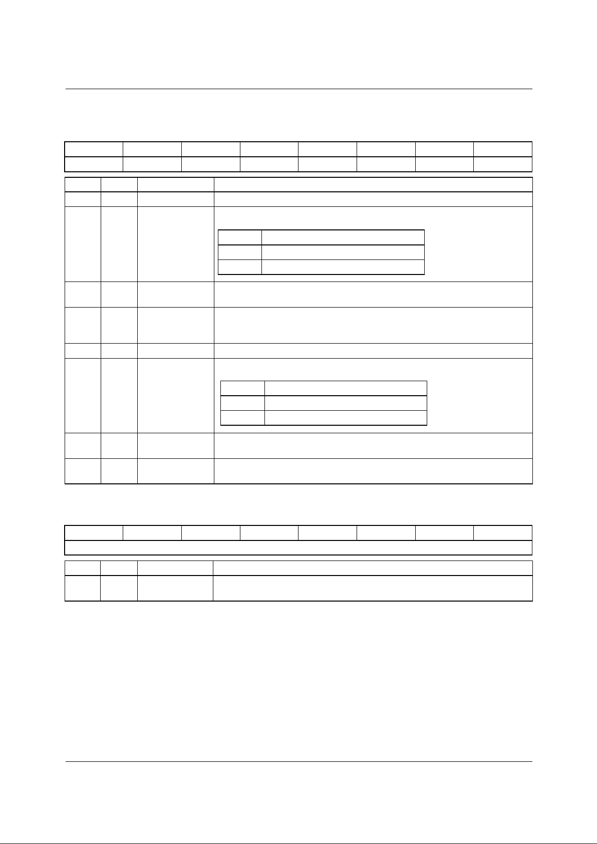
Luma Processor Control (06)
76543210
Reserved ANEN ANR ANT YSEL NOTCH
Reg Bit Name Description
06 7-6 Reserved Reserved, set to zero.
06 5 ANEN Adaptive notch enable. Enables adaptive notch when HIGH.
06 4 ANR Adaptive notch rounding. Sets adaptive notch rounding point.
06 3-2 ANT Adaptive notch threshold level. Sets the adaptive notch threshold.
06 1 YSEL Adaptive notch select. Selects adaptive notch filter response.
06 0 NOTCH Notch enable. Adaptive notch filter ANF3 selected when HIGH and ANEN is
HIGH, non-adaptive notch filter selected when HIGH and ANEN is LOW.
Function may be overridden by XSF (Reg 0E, bits 5-4).
ANR Function
0 Round to 10 bits
1 Round to 8 bits
ANT Function
00 Magnitude difference less than 32
01 Magnitude difference less than 24
10 Magnitude difference less than 16
11 Magnitude difference less than 8
YSEL Function
0 Adaptive notch response ANF1
1 Adaptive notch response ANF2
TMC22x5yA PRODUCT SPECIFICATION
16 REV. 1.0.0 2/4/03
Control Register Definitions (continued)
Comb Processor Control (07)
76543210
LS1BY LS1IN LS2DLY SPLIT BSFBY BSFSEL BSFMSB GRSDLY
Reg Bit Name Description
07 7 LS1BY Line store 1 bypass. Bypasses linestore 1 when HIGH.
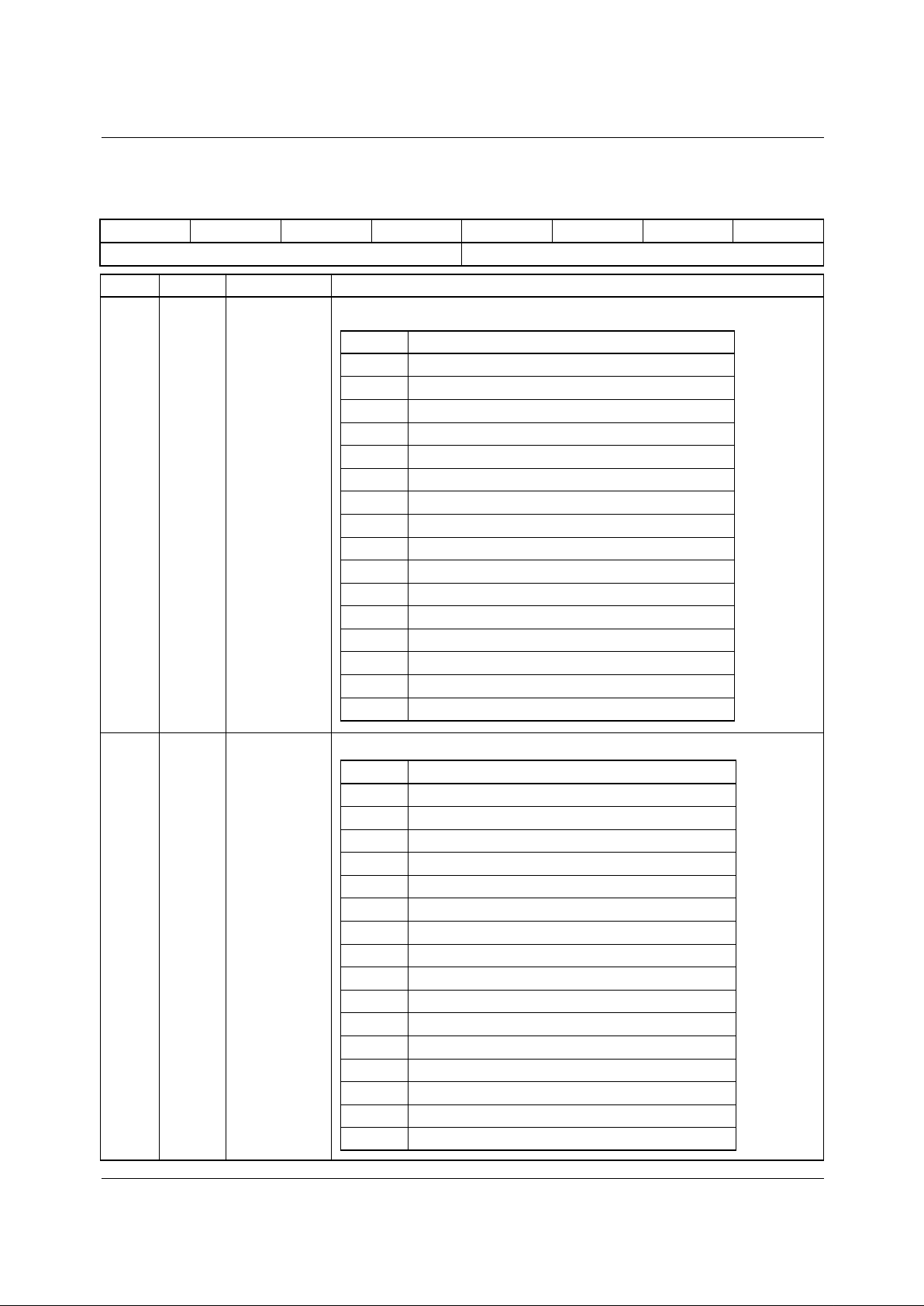
07 6 LS1IN Line store 1 input. Selects the input of linestore 1:
07 5 LS2DLY Line store 2 delay. LSTORE2 uses STS to store 1H when LOW and uses
VL to store SAV to EAV (or max count) when HIGH.
07 4 SPLIT Line store 2 delay. Splits data through LSTORE2, 9 bits chroma and 7 bits
luma when HIGH (chroma combs) and 8 bits chroma and 8 bits luma when
LOW (luma comb).
07 3 BSFBY Bandsplit filter bypass. Bandsplit filter is bypassed when HIGH.
07 2 BSFSEL Bandsplit filter select. Selects the bandsplit filter to be used:
07 1 BSFMSB Inverts msb of bandsplit filter. When HIGH, inverts the msb of the input to
the bandsplit filter.
07 0 GRSDLY Delays input to GRS decode. When HIGH, delays the input to the GRS
extraction circuit by 1H. Genlock only.
Mid-Sync Level (08)
76543210
MIDS
Reg Bit Name Description
08 7-0 MIDS Mid sync level. Sets the mid point of syncs for the mixed sync separator, in
the subcarrier locked mode.
LS1IN Function
0 Primary Input
1 Secondary Input
BSFSEL Function
0 Select bandsplit filter response 1
1 Select bandsplit filter response 2
PRODUCT SPECIFICATION TMC22x5yA
REV. 1.0.0 2/4/03 17
Control Register Definitions (continued)
Extended DRS (09)
76543210
PCKF VSTD
Reg Bit Name Description
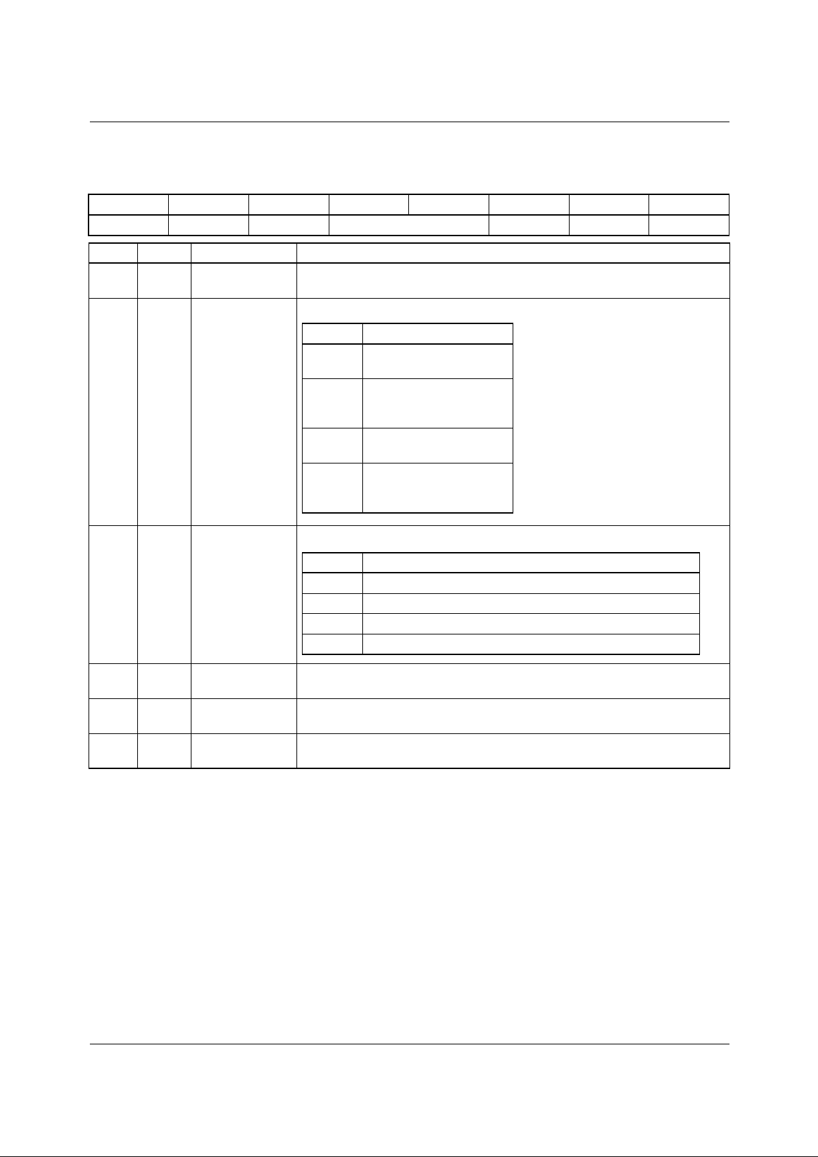
09 7-4 PCKF Clock rate.
09 3-0 VSTD Video Standard. Selects the video standard.
PCKF Function
0000 13.50 MHz
0001 reserved
0010 reserved
0011 reserved
0100 14.32 MHz
0101 17.73 MHz
0110 reserved
0111 reserved
1000 12.27 MHz
1001 14.75 MHz
1010 15.00 MHz
1011 reserved
1100 reserved
1101 reserved
1110 reserved
1111 reserved
VSTD Function
0000 NTSC-M
0001 NTSC-EIAJ
0010 reserved
0011 reserved
0100 reserved
0101 reserved
0110 reserved
0111 reserved
1000 PAL-B, G, H, I
1001 PAL-M
1010 PAL-N (Argentina, Paraguay, Uruguay)
1011 PAL-N (Jamaica)
1100 reserved
1101 reserved
1110 reserved
1111 reserved
TMC22x5yA PRODUCT SPECIFICATION
18 REV. 1.0.0 2/4/03
Control Register Definitions (continued)
Notes:
1. To enable “super blacks” and disable syncs of the output simply set MSEN[1] HIGH and the sync gain to zero.
Output Control (0A)
76543210
OP8B OPLMT OPLMT MSEN OPCMSB YBAL BUREN
Reg Bit Name Description
0A 7 OP8B Output rounded to 8 bits. Rounds the outputs to 8 bits when HIGH. The two
lsbs are set to zero.
0A 6-5 OPLMT Output limit select. Sets the output format and limiters:
0A 4-3 MSEN Mixed sync enable. Sets composite sync output format:
0A 2 OPCMSB Chroma output msb invert. Inverts the msb of the C
BCR
or Chroma output
when HIGH.
0A 1 YBAL Luma color correction. Setting this bit HIGH forces the chroma to zero
whenever the luma equals or exceeds the luma limit.
0A 0 BUREN Output burst enable. When HIGH, passes the burst through on the chroma
channel. Sets the burst region to zero when LOW.
OPLMT Function
00 RGB output format
limited to 4 to 1016
01 YCBCR output format
Y limited to 4 to 1016
CBCR limited to ±504
10 RGB output format
limited to 4 to 1016
11 YCBCR output format
Y limited to 64 to 940
CBCR limited to ±448
MSEN Function
00 No sync, & “super blacks” disabled
01 No sync, & “super blacks” disabled
10 Sync on G/Y output only, & “super blacks” enabled
11 Sync on RGB outputs, & “super blacks” enabled

PRODUCT SPECIFICATION TMC22x5yA
REV. 1.0.0 2/4/03 19
Control Register Definitions (continued)
Output Control (0B)
76543210
FMT422 CDEC YUVT Reserved DRSEN DRSCK
Reg Bit Name Description
0B 7 FMT422 Enables C
BCR
output mux. When HIGH, multiplexes the CB and CR data
onto the same data bus. The chroma or multiplexed C
BCR
output appears on
the B/C
B
output. The R/CR output is forced low.
0B 6 CDEC C
BCR
decimation enable. When HIGH, the CBCR data are decimated to
0:2:2 in the output processor.
0B 5 YUVT Enables D1 output. When HIGH, enables 4:2:2 multiplexed YC
BCR
onto the
R/CR data output with TRS words inserted into the output data stream. The Y
data are still available on the G/Y output and multiplexed CBCR is available on
the B/U output.
0B 4-2 Reserved Reserved, set to zero.
0B 1 DRSEN DRS output enable. When HIGH, enables the DRS onto the G/Y output.
0B 0 DRSCK DRS data rate. Sets the DRS output data rate.
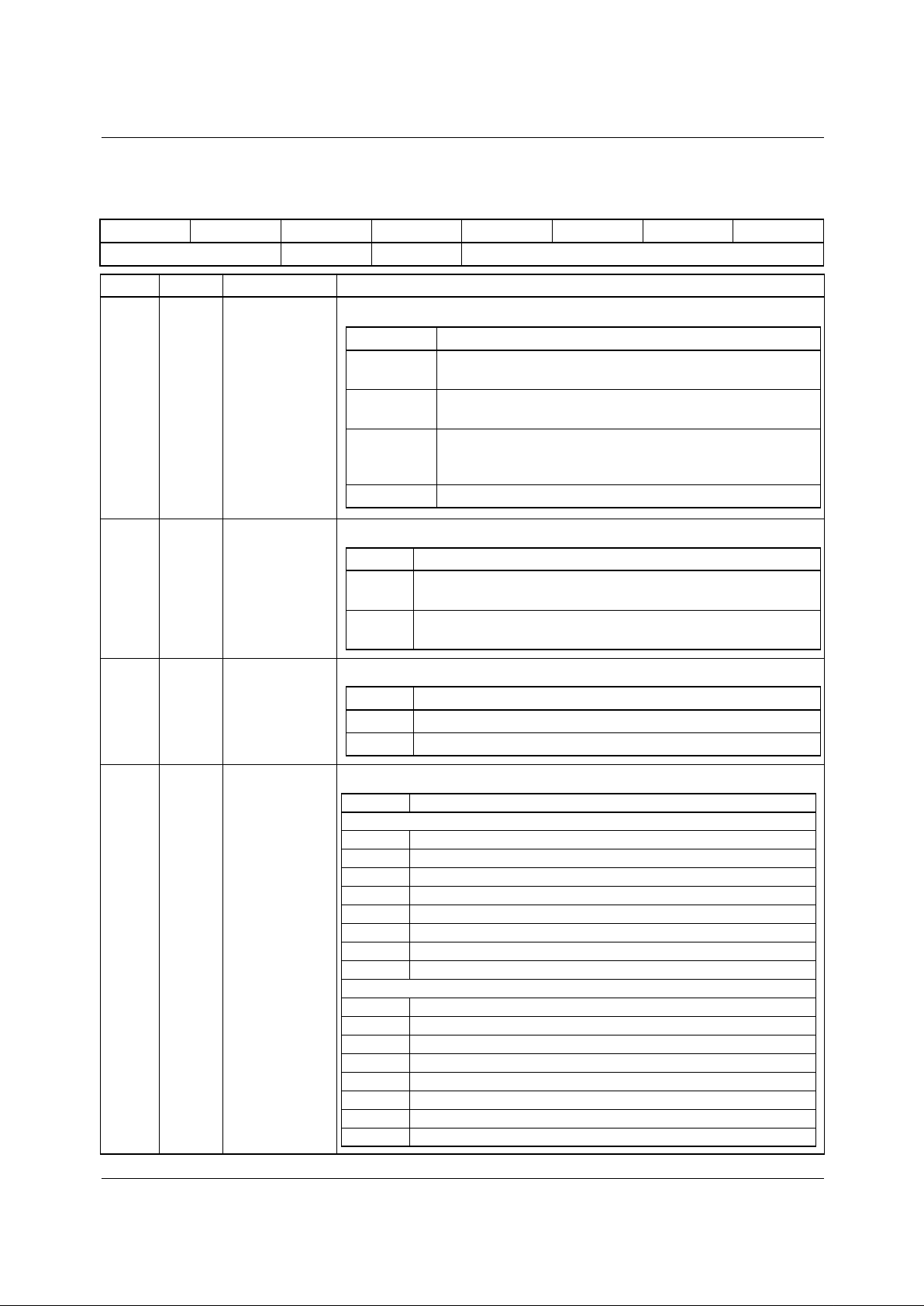
DRSCK Function
0 Embeds data bytes (8 bits) at PCK
clock rate
1 Embeds data nibbles (4 bits) at
PXCK clock rate
TMC22x5yA PRODUCT SPECIFICATION
20 REV. 1.0.0 2/4/03
Control Register Definitions (continued)
Comb Filter Control (0C)
76543210
ADAPT YCES YCSEL COMB
Reg Bit Name Description
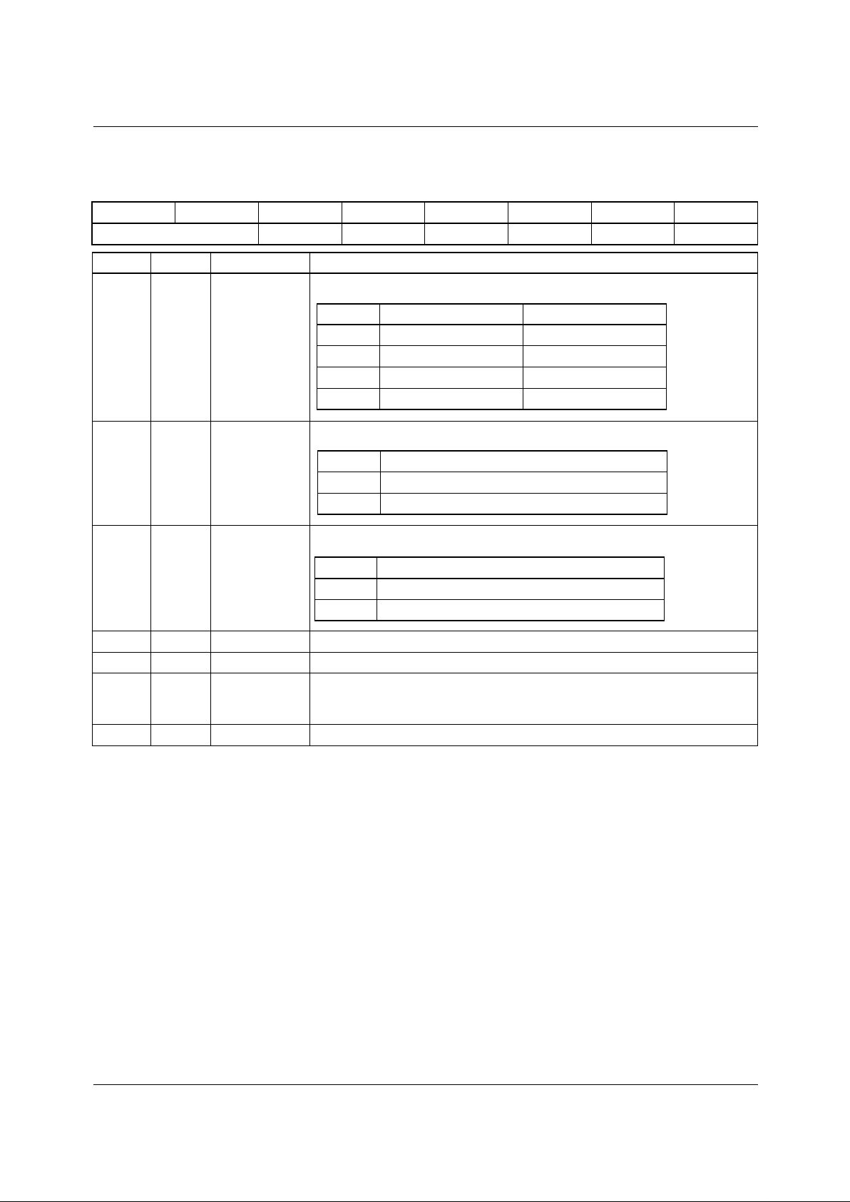
0C 7-6 ADAPT Adaption mode. Sets the 3-line comb filter adaption mode in NTSC.
0C 5 YCES YC input error signal control. Error signal control for YC input, luma comb.
0C 4 YCSEL Luma/chroma comb filter select. Selects luma or chroma comb filter.
0C 3-0 COMB Comb filter architecture.
ADAPT[1:0] Function
00 Adapts to best of 3 types of line based comb filters in NTSC
only.
01 Adapts to the best of two field or frame based comb filters
in NTSC only.
10 3 line (tap) comb only. Never adapts to a 2 line (tap) filter.
The higher set of comb filter error signals are sent to the
XLUT. NTSC or PAL comb filter.
11 Adapts to best of two 3 line chroma comb filters in PAL only.
YCES Function
0 LPF and HPF error signal, between (0H & 1H) or (1H & 2H) in
NTSC or between (0H & 2H) in PAL,are sent to XLUT
1 LPF error signal, between (0H & 1H) and (1H & 2H) in NTSC or
between (0H & 2H) in PAL, are sent to XLUT
YCSEL Function
0 Chroma comb filter
1 Luma comb filter
COMB Function
YC or composite comb filter architectures
0000 PAL or NTSC 3 line comb
0001 NTSC 3 line comb (0H & 1H)
0010 NTSC 3 line comb (1H & 2H)
0011 NTSC 2 line comb (0H & 1H)
0100 NTSC (2 line) field comb
0101 NTSC or PAL field comb
0110 NTSC (2 line) frame comb
0111 NTSC frame comb
D1 comb filter architectures
1000 3 line comb
1001 3 line comb (0H & 1H)
1010 3 line comb (1H & 2H)
1011 3 line comb (0H & 2H)
1100 (2 line) field comb
1101 field or 2 line (0H & 1H) comb
1110 (2 line) frame comb
1111 frame comb
PRODUCT SPECIFICATION TMC22x5yA
REV. 1.0.0 2/4/03 21
Control Register Definitions (continued)
Comb Filter Control (0D)
76543210
CEST CESG YESG CESTBY XFEN FAST YWBY
Reg Bit Name Description
0D 7-6 CEST Chroma error signal transform.
0D 5 CESG Chroma error signal gain.
0D 4 YESG Luma error signal gain.
0D 3 CESTBY Chroma error signal bypass. When HIGH, bypasses chroma error signal.
0D 2 XFEN XLUT filter enable. When HIGH, enables the LPF on the XLUT output.
0D 1 FAST Adaption speed select. When HIGH, the 3 line comb filter selects between
comb filter architectures on a pixel by pixel basis. When LOW, the selection
is filtered.
0D 0 YWBY Luma weighting bypass. When HIGH bypasses the luma fail weighting.
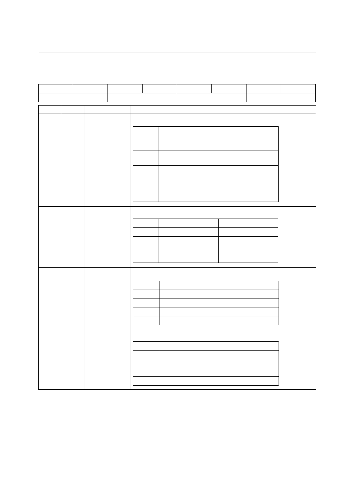
CEST Video Standard Clock Rate (MHz)
00 PAL/NTSC 4*Fsc & 13.5MHz
01 NTSC 12.27MHz
10 PAL 14.75MHz
11 PAL 15MHz
CESG Function
0 Normal chroma fail signal levels
1 Double the chroma error signal levels
YESG Function
0 Normal luma fail signal levels
1 Double the luma error signal levels
TMC22x5yA PRODUCT SPECIFICATION
22 REV. 1.0.0 2/4/03
Control Register Definitions (continued)
Comb Filter Control (0E)
76543210
XIP XSF YMUX CMUX
Reg Bit Name Description
0E 7-6 XIP XLUT input select. Selects the comb fail signals presented to the XLUT:
0E 5-4 XSF XLUT special function.
0E 3-2 YMUX Y output select. Output selection of luma 4:1 mux
0E 1-0 CMUX C output select. Output selection of chroma 4:1 mux
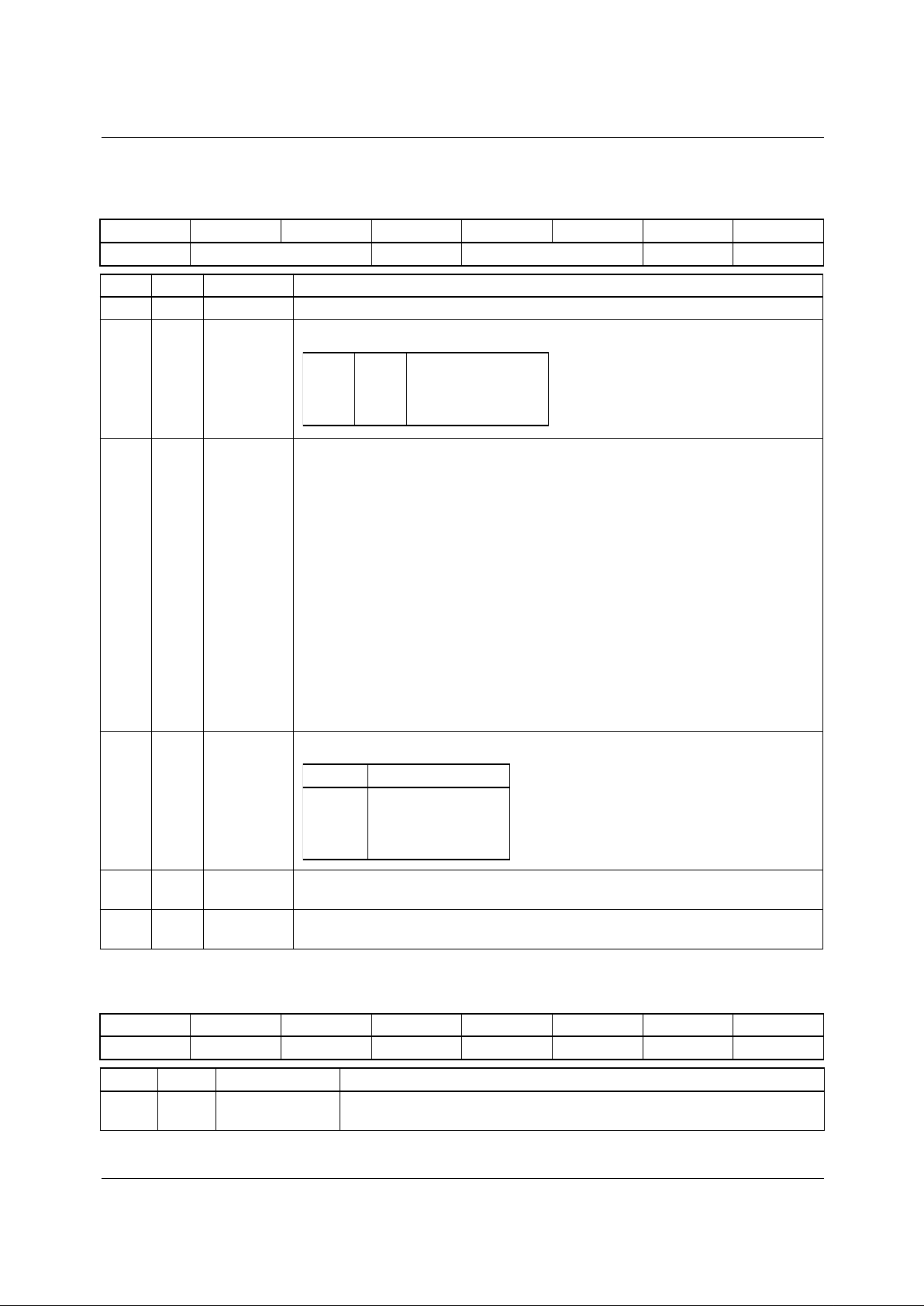
XIP[1:0] Input to XLUT
00 2 bits of phase error (X[7:6]), 3 bits of chroma
(X[5:3]) and luma magnitude error (X[3:0]).
01 4 bits of chroma (X[7:4]) and luma magnitude
error (X[3:0]).
10 3 bits of phase error (X[7:5]), 3 bits of chroma
magnitude error (X[4:2]), and 2 bits of luma
magnitude error (X[1:0]).
11 4 bits of phase error (X[7:4]) and chroma
magnitude error (X[3:0]).
XSF Luma Chroma
00 Comb Simple
01 Simple Comb
10 Flat with notch Simple
11 Flat with notch Comb
YMUX Output
00 Comb
01 Flat - Comb
10 Flat
11 Simple
CMUX Output
00 Comb
01 Flat - Comb
10 Flat
11 Simple
PRODUCT SPECIFICATION TMC22x5yA
REV. 1.0.0 2/4/03 23
Control Register Definitions (continued)
Comb Filter Control (0F)
76543210
Reserved CAT DCES IPCF YCCOMP SYNC
Reg Bit Name Description
0F 7 Reserved Reserved, set to zero.
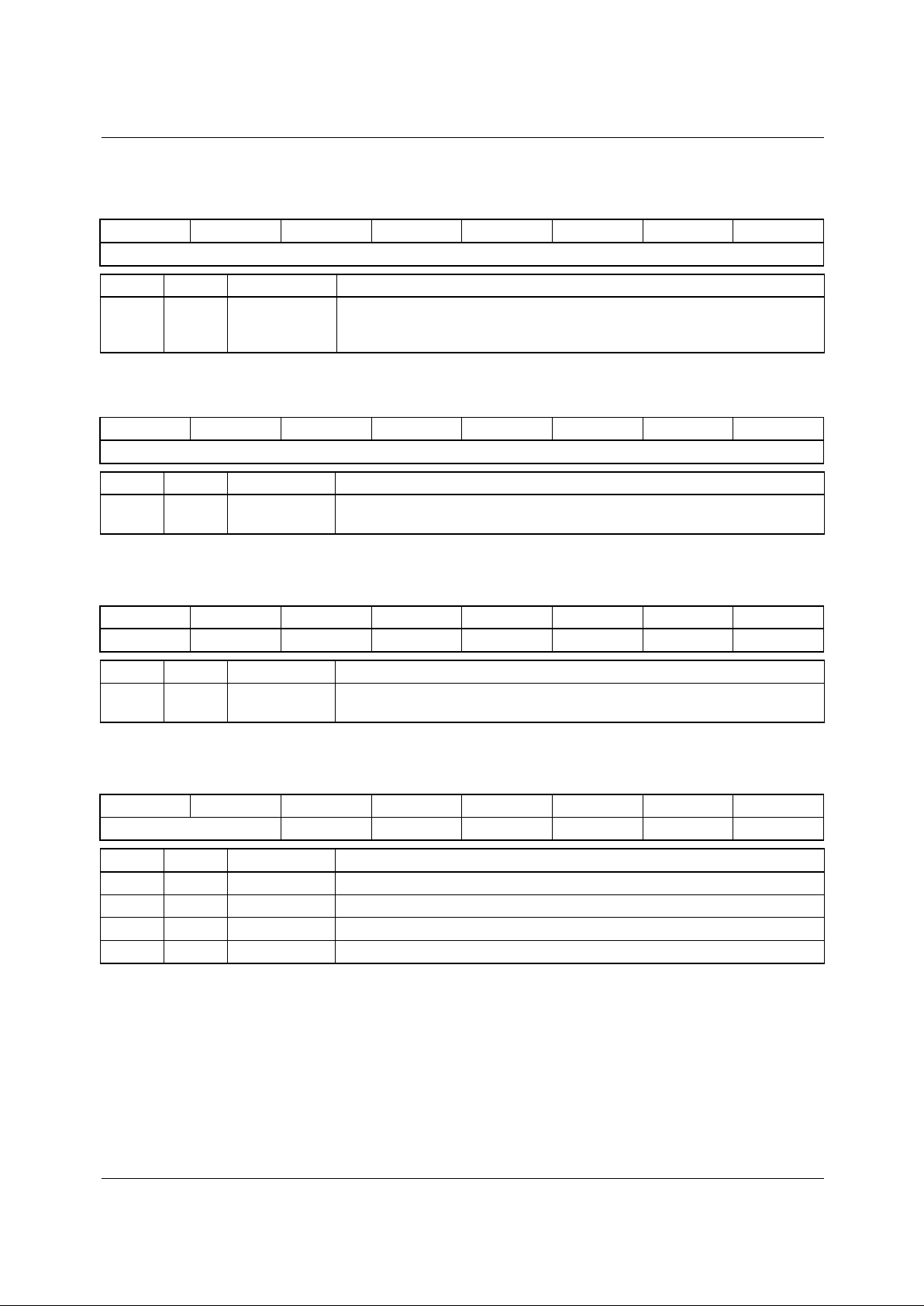
0F 6-5 CAT Adaption threshold. Fixes threshold at which different comb filters are selected.
0F 4 DCES D1 C
BCR
error signal. When set LOW for D1 chroma comb filters:
a) In 3 line comb filter architectures, the magnitude error between the component
data for that pixel selects the 3 line comb or adapts to a
2 line comb. On a “CB pixel” the error signal selected on pixel (x+4) is sent to
the XLUT with the magnitude difference between “CR pixels” on the same pair
of lines, but from pixel (x+3). Likewise on a “CR pixel” the error signal selected
on pixel (x+5) is sent to the XLUT with the magnitude difference between “CB
pixels” on the same lines but from pixel (x+4).
b) In 2 line comb filters the magnitude differences between the same pair of lines
is always sent to the XLUT, On a “CB pixel” the error from the preceding “CR
pixel” is used and on a “CR pixel” the preceding “CB pixel” would be used.
When set HIGH for D1 chroma filters:
This is used for 3 line comb filter architecture that are inhibited from adapting to 2
line comb filter architectures. The input to the XLUT is the magnitude error in C
R
between (0H & 1H) and (1H & 2H) on “CR pixels” and the magnitude error
between (0H & 1H) and (1H & 2H) on “CB pixels”.
0F 3-2 IPCF Comb filter input select. Selects primary inputs to the comb filter.
0F 1 YCCOMP YC or Composite input select. Selects YC inputs when HIGH and composite
inputs when LOW.
0F 0 SYNC Sync processor select. The syncs are obtained by a LPF when HIGH and by the
comb filter when LOW.
Sync Pulse Generator (10)
76543210
STS
7
STS
6
STS
5
STS
4
STS
3
STS
2
STS
1
STS
0
Reg Bit Name Description
10 7-0 STS
7-0
Sync to sync 8 lsbs. Bottom 8 bits of the number of pixels between sync
pulses.
0
0
1
1
0
1
0
1
5% of max error
15% of max error
25% of max error
50% of max error
IPCF Function
0 0
0 1
1 0
1 1
Flat video
LPF output
HPF output
Reserved
TMC22x5yA PRODUCT SPECIFICATION
24 REV. 1.0.0 2/4/03
Control Register Definitions (continued)
Sync Pulse Generator (11)
76543210
STB
Reg Bit Name Description
11 7-0 STB Sync to burst. Controls the number of pixels from sync to burst. This signal
starts the burst sample and hold. In SC mode, subtract 25 from the desired
delay to generate this value.
Sync Pulse Generator (12)
76543210
BTV
Reg Bit Name Description
12 7-0 BTV Burst to video. Controls the number of pixels from STB to the start of active
video.
Sync Pulse Generator (13)
76543210
AV
7
AV
6
AV
5
AV
4
AV
3
AV
2
AV
1
AV
0
Reg Bit Name Description
13 7-0 AV
7-0
Active video line 8 lsbs. Bottom 8 bits of the number of pixels during the
active video line.
Sync Pulse Generator (14)
76543210
Reserved AV
9
AV
8
Reserved STS
10
STS
9
STS
8
Reg Bit Name Description
14 7-6 Reserved Reserved, set to zero.
14 5-4 AV
9-8
Active video line 2 msbs. Two most significant bits of AV.
14 3 Reserved Reserved, set to zero.
14 2-0 STS
10-8
Sync to sync 3 msbs. Three most significant bits of STS.
PRODUCT SPECIFICATION TMC22x5yA
REV. 1.0.0 2/4/03 25
Control Register Definitions (continued)
Sync Pulse Generator (15)
76543210
Reserved VINDO VDIV VDOV
Reg Bit Name Description
15 7 Reserved Reserved, set to zero.
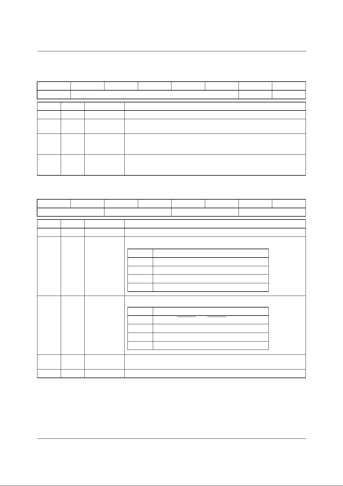
15 6-2 VINDO Number of lines in vertical window. The number of lines (0 to 31) after the
last EQ pulse that the decoder passes through the Vertical INterval winDOw.
15 1 VDIV Action inside VINDO. The vertical data inside the `VINDO' is passed
through a simple decoder when LOW, or is passed unprocessed on the luma
channel with the chroma channel set to zero when HIGH.
15 0 VDOV Action outside VINDO. The vertical data after the `VINDO' and before the
end of vertical blanking is blanked (YUV = 0) when LOW, or passed through
the simple decoder when HIGH.
Sync Pulse Generator (16)
76543210
Reserved NFDLY SPGIP MSIP
Reg Bit Name Description
16 7-6 Reserved Reserved, set to zero.
16 5-4 NFDLY new field detect delay. NTSC frame detect delay:
16 3-2 SPGIP SPG input select. Selects the input to the Sync Pulse Generator:
16 1 MSIP Mixed sync separator input. Set HIGH for external VIDEOB reference or
LOW for output of Low Pass Filter.
16 0 SMO State Machine Offset. Set HIGH for a 1H offset and LOW for a 0H offset.
NFDLY Function
00 pixel count = 0
01 pixel count = 1
10 pixel count = 2
11 pixel count = 3
SPGIP Input
00 External HSYNC and VSYNC
01 Digitized sync (subcarrier mode)
10 TRS words embedded in the D1 data stream
11 TRS words embedded in the D2 data stream
TMC22x5yA PRODUCT SPECIFICATION
26 REV. 1.0.0 2/4/03
Control Register Definitions (continued)
Buffered register set 0 (17) Active when BUFFER pin set LOW.
76543210
SG0
7
SG0
6
SG0
5
SG0
4
SG0
3
SG0
2
SG0
1
SG0
0
Reg Bit Name Description
17 7-0 SG0
7-0
Msync gain, 8 lsbs. Bottom 8 bits of mixed sync scalar
lsb = 1/256
Buffered register set 0 (18) Active when BUFFER pin set LOW.
76543210
YG0
7
YG0
6
YG0
5
YG0
4
YG0
3
YG0
2
YG0
1
YG0
0
Reg Bit Name Description
18 7-0 YG0
7-0
Y gain, 8 lsbs. Bottom 8 bits of the luma gain
lsb = 1/256
Buffered register set 0 (19) Active when BUFFER pin set LOW.
76543210
UG0
7
UG0
6
UG0
5
UG0
4
UG0
3
UG0
2
UG0
1
UG0
0
Reg Bit Name Description
19 7-0 UG0
7-0
U gain, 8 lsbs. Bottom 8 bits of the U gain
lsb = 1/256
Buffered register set 0 (1A) Active when BUFFER pin set LOW.
76543210
VG0
7
VG0
6
VG0
5
VG0
4
VG0
3
VG0
2
VG0
1
VG0
0
Reg Bit Name Description
1A 7-0 VG0
7-0
V gain, 8 lsbs. Bottom 8 bits of the V gain
lsb = 1/256
Buffered register set 0 (1B) Active when BUFFER pin set LOW.
76543210
YG0
9
YG0
8
UG0
10
UG0
9
UG0
8
Reserved VG0
9
VG0
8
Reg Bit Name Description
1B 7-6 YG0
9-8
Y gain, 2 msb. Top 2 bits of the Y gain. msb = 2
1B 5-3 UG0
10-8
U gain, 3 msbs. Top 3 bits of the U gain. msb = 4
1B 2 Reserved Reserved, set to zero.
1B 1-0 VG0
9-8
V gain, 2 msbs. Top 2 bits of the V gain. msb = 2
 Loading...