Fairchild Semiconductor TMC2192 Datasheet
TMC2192
10 Bit Encoder
www.fairchildsemi.com
Features
• Multiple input formats
– 20 bit CCIR601
– 10 bit CCIR656
– 10 bit Digital Composite
• Synchronization modes
– Master
– Slave
– Genlock
– CCIR656
• Subcarrier modes
– Free-run
– Subcarrier reset
– Genlock
– DRS-lock
• Ancillary Data Control (ANC)
• Pixel rates from 10 MHz to 15 MHz
• Programmable horizontal timing
• Programmable vertical blanking interval (VBI)
• Line-by-line pedestal enable
• Programmable pedestal height from -20 IRE to 20 IRE
• Programmable burst amplitude and phase
• Controlled edge rates for
– Sync
– Burst
– Active video
• Programmable color space matrix
• 8:8:8 video reconstruction
• Three 10 bit D/A’s with independent trim
• Individual power down modes for each D/A
• Multiple output formats
– S-video
– Composite
– Digital composite output
• Pin-driven and data-driven, window keying
• Closed Caption waveform generation (13.5 MHz only)
• Sin(X)/X compensation filter
• 5 bit VBI line counter
• 3 bit field counter
• Internal test pattern generation
– 100% Color Bars
– 75% Color Bars
– Modulated Ramp
Applications
• Broadcast Television
• Nonlinear Video Processing
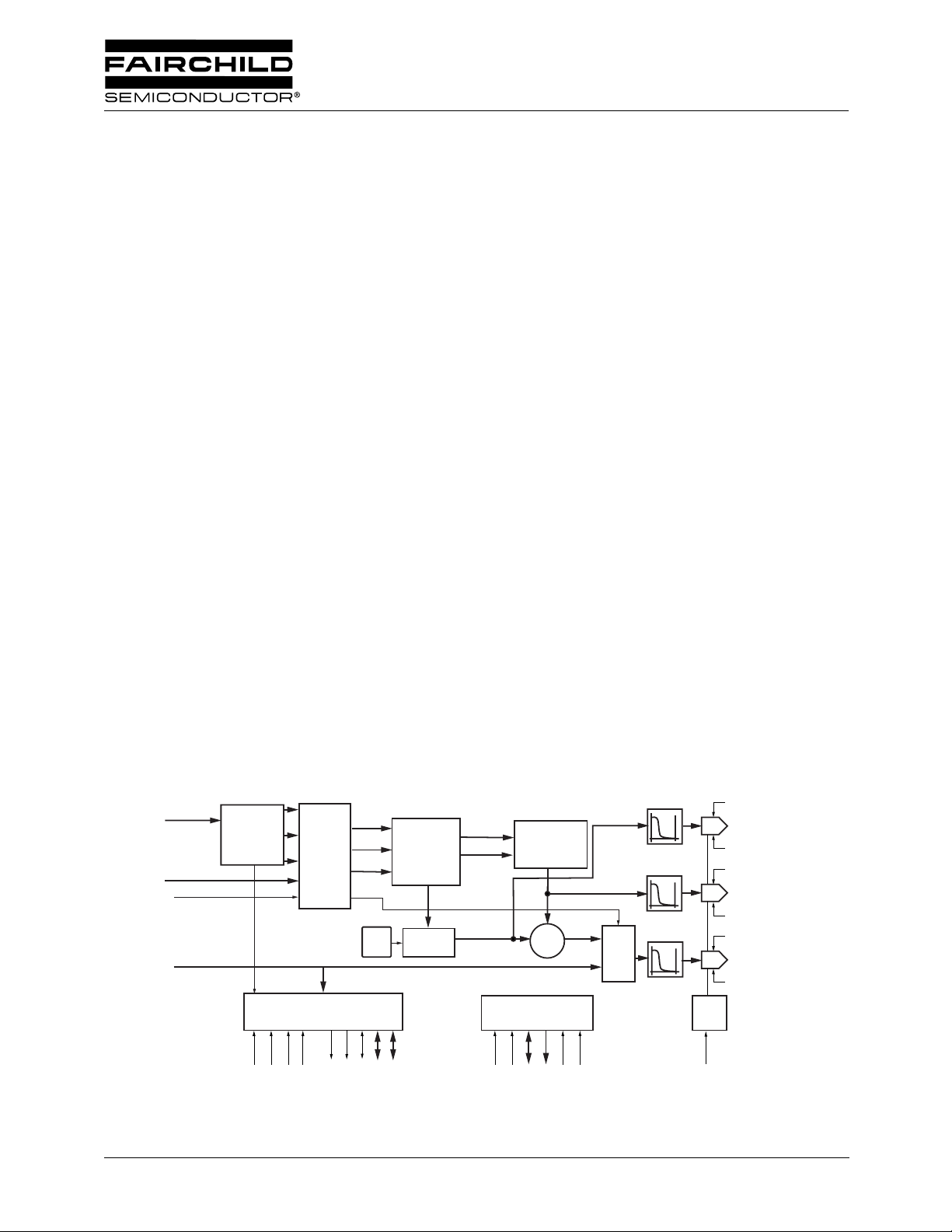
Block Diagram
PD[23:0]
PROCESSER
OL[4:0]
KEY
CVBS[9:0]
PRE-
PXCK
HSIN
OVERLAY
MIXER
FVHGEN
VSIN
DCVEN\
VSOUT
HSOUT
y
cb
cr
Gain
Adjustment
FLD[2:0]
LINE[4:0]
SYNC
INSERT
CC
PDCIN/PDCOUT
C
BYP
LUMA
DAC
REF.
2194001a
LUMA
R
C
CHROMA
R
C
COMPOSITE
R
VREF
REF
BYP
REF
BYP
REF
LUMA
LUMA
CHROMA
COMP
COMP
U
Chroma
V
Modulator
Y
+
MPU
D[7:0]
SERB
RESET
CS/SCL
R/W\/SDA
A[1:0]/SA[1:0]
INTERP.
INTERP.
KEY
MIX
INTERP.
REV. 1.0.0 8/13/03

TMC2192 PRODUCT SPECIFICATION
Table of Contents
Features . . . . . . . . . . . . . . . . . . . . . . . . . . . .1
Applications. . . . . . . . . . . . . . . . . . . . . . . . .1
Block Diagram . . . . . . . . . . . . . . . . . . . . . . .1
10 Bit Encoder . . . . . . . . . . . . . . . . . . . . . . .1
List of Figures . . . . . . . . . . . . . . . . . . . . . . .3
List of Tables . . . . . . . . . . . . . . . . . . . . . . . .3
Pin Assignments . . . . . . . . . . . . . . . . . . . . .4
Pin Definitions . . . . . . . . . . . . . . . . . . . . . . .4
Functional Description . . . . . . . . . . . . . . . .7
Input Formats. . . . . . . . . . . . . . . . . . . . . . . . . . . 7
Color Space Matrix . . . . . . . . . . . . . . . . . . . . . . 9
Synchronization Modes . . . . . . . . . . . . . . . . . 10
Propagation Delay . . . . . . . . . . . . . . . . . . . . . . 10
Blanking Control . . . . . . . . . . . . . . . . . . . . . . . 11
Pixel Data Control . . . . . . . . . . . . . . . . . . . . . . 11
Edge Shaping. . . . . . . . . . . . . . . . . . . . . . . . . . 11
Horizontal Programming. . . . . . . . . . . . . . . . . 12
Vertical Timing . . . . . . . . . . . . . . . . . . . . . . . . . 15
Chrominance Processor . . . . . . . . . . . . . . . . . 21
Subcarrier Programming. . . . . . . . . . . . . . . 21
NTSC Subcarrier . . . . . . . . . . . . . . . . . 21
PAL Subcarrier . . . . . . . . . . . . . . . . . . . 21
PAL-M Subcarrier . . . . . . . . . . . . . . . . . 21
Subcarrier Synchronization. . . . . . . . . . . . . 22
SCH Phase Error Correction. . . . . . . . . . . . 22
Burst Envelope . . . . . . . . . . . . . . . . . . . . . . 23
Color-Difference Low-Pass Filters. . . . . . . . 23
Sync and Pedestal Insertion. . . . . . . . . . . . . . 23
Pedestal Enable . . . . . . . . . . . . . . . . . . . . . 23
Pedestal Height. . . . . . . . . . . . . . . . . . . . . . 24
Sync and Blank Insertion . . . . . . . . . . . . . . 24
Interpolation Filters . . . . . . . . . . . . . . . . . . . . . 25
x/Sin(x) Filter . . . . . . . . . . . . . . . . . . . . . . . . . . 25
Output Data Formats. . . . . . . . . . . . . . . . . . . . 25
Digital Composite Output . . . . . . . . . . . . . . . . 26
Ancillary Data. . . . . . . . . . . . . . . . . . . . . . . . . . 26
Operating Modes. . . . . . . . . . . . . . . . . . . . . 27
Layering Engine. . . . . . . . . . . . . . . . . . . . . . . . 28
Overlay Mixer . . . . . . . . . . . . . . . . . . . . . . . 28
Hardware Keying . . . . . . . . . . . . . . . . . . . . . . . 29
Data Keying . . . . . . . . . . . . . . . . . . . . . . . . . . . 29
Parallel Microprocessor Interface . . . . . . . . . 29
Serial Control Port (R-Bus). . . . . . . . . . . . . . . 31
Data Transfer via Serial Interface . . . . . . . . 31
Serial Interface Read/Write Examples . . . . 31
Control Register Map . . . . . . . . . . . . . . . . 33
Control Register Definitions . . . . . . . . . . 35
Absolute Maximum Ratings. . . . . . . . . . .60
Operating Conditions . . . . . . . . . . . . . . . . 60
Electrical Characteristics . . . . . . . . . . . . .62
Switching Characteristics . . . . . . . . . . . .62
System Performance Characteristics . . . 63
Applications Discussion . . . . . . . . . . . . . 63
Layout Considerations . . . . . . . . . . . . . . . . . . 64
Output Low-Pass Filters . . . . . . . . . . . . . . . . . 67
Mechanical Dimensions . . . . . . . . . . . . . . 71
100-Lead MQFP . . . . . . . . . . . . . . . . . . . . . . . . 71
Ordering Information . . . . . . . . . . . . . . . .72
Life Support Policy . . . . . . . . . . . . . . . . . . 72
Closed Caption Insertion . . . . . . . . . . . . . . . . 24
Line Selection . . . . . . . . . . . . . . . . . . . . . . . 24
Parity Generation . . . . . . . . . . . . . . . . . . . . 24
Operating Sequence . . . . . . . . . . . . . . . . . . 24
2 REV. 1.0.0 8/13/03

PRODUCT SPECIFICATION TMC2192
List of Figures
Figure 1. Input Formats . . . . . . . . . . . . . . . . . . . . . .7
Figure 2. 24 bit Input Format . . . . . . . . . . . . . . . . . .7
Figure 3. CCIR656 Input Format . . . . . . . . . . . . . . .8
Figure 4. 10 bit Input Format . . . . . . . . . . . . . . . . . .8
Figure 5. 20 bit 4:2:2 Input Format . . . . . . . . . . . . .8
Figure 6. 20 bit 4:4:4 Input Format . . . . . . . . . . . . .8
Figure 7. Propagation Delay through the
Encoder . . . . . . . . . . . . . . . . . . . . . . . . .10
Figure 8. Horizontal Timing . . . . . . . . . . . . . . . . . .13
Figure 9. Horizontal Timing – Vertical Blanking . . .13
Figure 10. Horizontal Timing – 1st Half-line. . . . . . .14
Figure 11. Horizontal Timing – 2nd Half-line . . . . . .14
Figure 12. NTSC Vertical Interval . . . . . . . . . . . . . .15
Figure 13. PAL Vertical Interval . . . . . . . . . . . . . . . .17
Figure 14. PAL-M Vertical Interval . . . . . . . . . . . . . .19
Figure 15. Burst Envelope . . . . . . . . . . . . . . . . . . . .23
Figure 16. Gaussian Filter Response . . . . . . . . . . .23
Figure 17. Interpolation Filter. . . . . . . . . . . . . . . . . .25
Figure 18. Interpolation Filter – Passband
Detail . . . . . . . . . . . . . . . . . . . . . . . . . . .25
Figure 19. X/SIN(X) Filter . . . . . . . . . . . . . . . . . . . .25
Figure 20. Layering Engine . . . . . . . . . . . . . . . . . . .28
Figure 21. Overlay Outputs . . . . . . . . . . . . . . . . . . .29
Figure 22. Data Keying . . . . . . . . . . . . . . . . . . . . . .29
Figure 23. Microprocessor Parallel Port –
Write Timing . . . . . . . . . . . . . . . . . . . . . .30
Figure 24. Microprocessor Parallel Port –
Read Timing . . . . . . . . . . . . . . . . . . . . . .30
Figure 25. Serial Port Read/Write Timing . . . . . . . .31
Figure 26. Serial Interface – Typical Byte
Transfer. . . . . . . . . . . . . . . . . . . . . . . . . .32
Figure 27. Serial Interface – Chip Address . . . . . . .32
Figure 28. Typical Analog Reconstruction Filter . . .63
Figure 29. Overall Response . . . . . . . . . . . . . . . . . .63
Figure 30. Typical Layout . . . . . . . . . . . . . . . . . . . . .65
Figure 31. ST-163E Layout . . . . . . . . . . . . . . . . . . .66
Figure 32. Pass Band . . . . . . . . . . . . . . . . . . . . . . .67
Figure 33. Stop Band. . . . . . . . . . . . . . . . . . . . . . . .67
Figure 34. 2T Pulse . . . . . . . . . . . . . . . . . . . . . . . . .67
Figure 35. Group Delay . . . . . . . . . . . . . . . . . . . . . .67
List of Tables
Table 1. CSM Coefficient Range . . . . . . . . . . . . . 9
Table 2. Expected Output Values for the
CSM with YCBCR Inputs . . . . . . . . . . . . 9
Table 3. PDC Edge Control . . . . . . . . . . . . . . . . 11
Table 4. Horizontal Line Equations. . . . . . . . . . . 12
Table 5. Horizontal Timing Specifications. . . . . . 13
Table 6. Vertical Interval Timing
Specifications . . . . . . . . . . . . . . . . . . . . 14
Table 7. Default Horizontal Timing
Parameters . . . . . . . . . . . . . . . . . . . . . . 15
Table 8. NTSC Field/Line Sequence and
Identification . . . . . . . . . . . . . . . . . . . . . 16
Table 9. PAL Field/Line Sequence and
Identification . . . . . . . . . . . . . . . . . . . . . 18
Table 10. PAL-M Field/Line Sequence and
Identification . . . . . . . . . . . . . . . . . . . . . 20
Table 11. Standard Subcarrier Parameters . . . . . 22
Table 12. Line by Line Pedestal Enable . . . . . . . . 23
Table 13. Closed Caption Line Selection . . . . . . . 24
Table 14. D/A Outputs . . . . . . . . . . . . . . . . . . . . . 25
Table 15. Ancillary Data Format . . . . . . . . . . . . . . 26
Table 16. Ancillary Data Control – Phase . . . . . . 27
Table 17. Ancillary Data Control Frequency. . . . . 27
Table 18. Field Identification and Subcarrier
Reset Modes . . . . . . . . . . . . . . . . . . . . 27
Table 19. Layering and Keying Modes . . . . . . . . . 28
Table 20. Overlay Address Map . . . . . . . . . . . . . . 29
Table 21. Parallel Port Control . . . . . . . . . . . . . . . 30
Table 22. Serial Port Addresses. . . . . . . . . . . . . . 31
Table 23. Control Register Map . . . . . . . . . . . . . . 33
REV. 1.0.0 8/13/03 3
TMC2192 PRODUCT SPECIFICATION
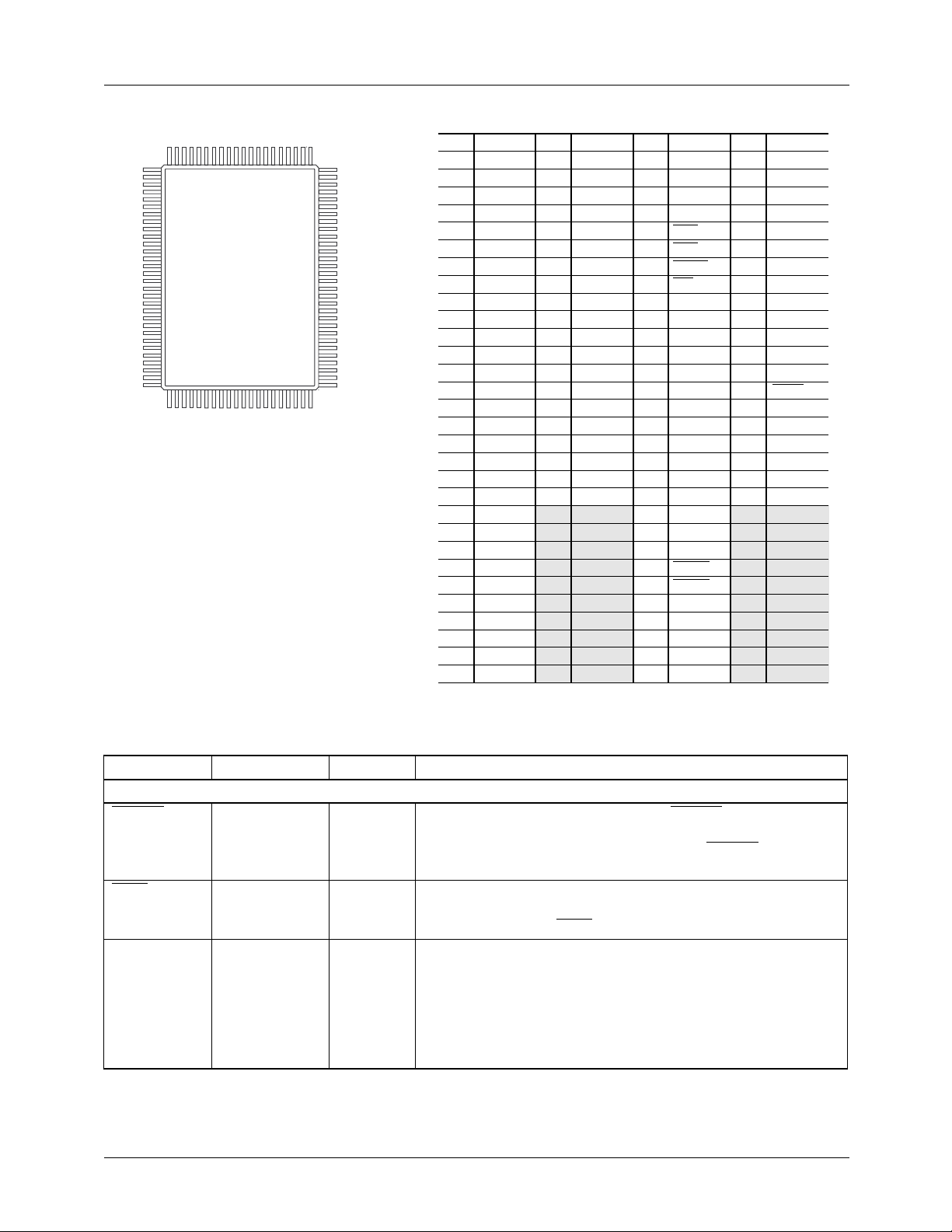
Pin Assignments
100 81
1
30
31 50
80
51
65-6294-14
Pin
1
2
3
4
5
6
7
8
9
10
11
12
13
14
15
16
17
18
19
20
21
22
23
24
25
26
27
28
29
30
Function
V
DDA
COMP
C
BYPCOMP
A
GND
CHROMA
C
BYPCHROM
V
DDA
R
REFCHROM
A
GND
LUMA
C
BYPLUMA
V
DDA
R
REFLUMA
A
GND
A
GND
V
DDA
V
DDA
A
GND
A
GND
KEY
OL4
OL3
OL
2
OL
1
OL0
D
GND
PD23
PD
22
PD
21
PD
20
Pin
31
32
33
34
35
36
37
38
39
40
41
42
43
44
45
46
47
48
49
50
Function
PD
19
PD
18
PD
17
PD16
PD
15
PD
14
PD13
PD12
V
DD
D
GND
PD
11
PD
10
PD9
PD8
PD
7
PD
6
PD5
PD4
PD
3
PD
2
Pin
51
52
53
54
55
56
57
58
59
60
61
62
63
64
65
66
67
68
69
70
71
72
73
74
75
76
77
78
79
80
Function Pin
PD1
PD0
D
GND
V
DD
VSIN
HSIN
DCVEN
SER
CS\/SCL
R/W\/SDA
A1/SA1
A0/SA0
D
7
D6
D
5
D
4
D3
D2
D
1
D0
D
GND
V
DD
PDC
HSOUT
VSOUT
LINE4
LINE3
LINE2
LINE1
LINE0
81
82
83
84
85
86
87
88
89
90
91
92
93
94
95
96
97
98
99
100
Function
FLD2
FLD1
FLD0
CVBS9
CVBS8
CVBS7
CVBS6
CVBS5
CVBS4
CVBS3
CVBS2
CVBS1
CVBS0
RESET
PXCK
V
D
V
R
AGND
DD
GND
REF
REFCOMP
Pin Definitions
Pin Name Pin Number Value Description
CLOCK, SYNC, & CONTROL INPUTS (6 pins)
DCVEN 57 TTL Digital CVBS Output Enable. When DCVEN is LOW, the
Comp2 output prior to the D/A is routed to D7-0, FLD2-1
providing a digital composite output. When DCVEN is HIGH,
D7-0 and FLD2-1 operate in their normal mode.
HSIN 56 TTL Horizontal Sync Input. When operating in slave, Genlock, or
DRS-Lock the TMC2192 will start a new horizontal line with
each falling edge of HSIN.
KEY 20 TTL Hard Key selection. When the control register bit HKEN is set
HIGH and the hardware KEY pin is high, the video data
considered to be the foreground. is routed to the COMP2
output. This control signal is data aligned so that the pixel that is
present on the PD port when KEY signal is latched is at the
midpoint of the key transition. When HKEN is LOW, Key is
ignored.
4 REV. 1.0.0 8/13/03

PRODUCT SPECIFICATION TMC2192
Pin Definitions (continued)
Pin Name Pin Number Value Description
PXCK 95 TTL Pixel Clock Input. PXCK is a clock signal that period is twice
the sample rate of the pixel data. The operating range is 20 to
30 MHz. The clock is internally divided by 2 to generate the
internal pixel clock, PCK. PXCK drives the entire TMC2192
except the asynchronous microprocessor interface.
RESET
VSIN
SYNC & CONTROL OUTPUTS (11 pins)
FLD[2:0] 81–83 TTL Field Identifier. Field Identifier outputs the current field number.
HSOUT 74 TTL Horizontal Sync Output. The alignment of HSOUT to the pixel
LINE[4:0] 76–80 TTL Vertical Blanking Interval Line Identifier. LINE identifies the
PDC 73 TTL Pixel Data Control.
94 TTL Master Chip Reset. When LOW, All outputs are tri-stated and
the internal state machines and control registers are reset. At
rising edge of RESET, all outputs are active, the preset values
will be loaded into the control registers and the internal states
machines start to operate.
55 TTL Vertical Sync Input. When operating in slave, Genlock, or
DRS-Lock the TMC2192 will start a new vertical field with each
falling edge of VSIN that is coincident with HSIN.
For all video standards the field identifier will cycle through the
eight counts.
data port or DCVBS port is controlled by control register
TSOUT.
current line number for the first 31 lines. If the line count is
greater than 31 then LINE is 11111b. The first line with a vertical
serration is considered to be line 0.
When PDCDIR = LOW: At a rising edge, The next pixel starts a
controlled ramp of the PD data. At a falling edge, the pixel prior
is the last PD used in the ramp. The rising edge is determined
by the PDCCNT control register, the falling edge of PDC is
determined by the horizontal timing registers.
When PDCDIR = HIGH: PDCIN is used to override the internal
PDC. When HIGH, the internal PDC controls the blank and
unblank window. When LOW, the video remains blanked
regardless of the internal PDC. All edges have the same ramp
control as the internal PDC.
VSOUT 75 TTL Vertical Sync Output. The alignment of VSOUT to the pixel
data port or DCVBS port is controlled by control register
TSOUT.
DATA INPUTS (39 pins)
CVBS[9:0] 84–93 TTL Composite Data Input
OL[4:0] 21–25 TTL Overlay Control
PD[23:0] 27–38, 41–52 TTL Component Data Input
ANALOG INTERFACE – Video Out (5 pins)
LUMA 10 1.35Vp-p Luma
CHROMA 5 1.35Vp-p Chroma
COMP 2 1.35Vp-p Composite D/A with optional keying
REV. 1.0.0 8/13/03 5

TMC2192 PRODUCT SPECIFICATION
Pin Definitions (continued)
Pin Name Pin Number Value Description
ANALOG INTERFACE – Support (9 pins)
C
BYPLUMA
C
BYPCHROM
C
BYPCOMP
R
REFLUMA
R
REFCHROM
R
REFCOMP
V
REF
MPU INTERFACE (13 pins)
A[1:0]/SA[1:0] 61, 62 TTL When SER (HIGH), OLUT/control/pointer address.
CS/SCL 59 TTL/R-BUS When SER (HIGH), microprocessor port clock.
D[7:0] 63–70 TTL Bi-directional Data Bus.
RW/SDA 60 TTL/R-BUS When SER (HIGH), read/write control.
SER 58 TTL Microprocessor Select. When LOW, the serial interface is
POWER & GROUND (17 pins)
A
GND
D
V
V
GND
DD
DDA
26, 40, 53, 71, 97 0.0V Digital ground
11 0.1 µF Reference Bypass Capacitor for LUMA DAC. Connection
point for 0.1 µF Capacitor.
6 0.1 µF Reference Bypass Capacitor for CHROMA DAC. Connection
point for 0.1 µF Capacitor.
3 0.1 µF Reference Bypass Capacitor for COMPOSITE DAC.
Connection point for 0.1 µF Capacitor.
13 1210 Ohm Current Setting Resistor. Connection point for external current
setting resistor for LUMA DAC. The resistor is connected
between R
inversely proportional to the value of R
8 1210 Ohm Current Setting Resistor. Connection point for external current
setting resistor for CHROMA DAC. The resistor is connected
between R
inversely proportional to the value of R
99 1210 Ohm Current Setting Resistor. Connection point for external current
setting resistor for COMPOSITE DAC. The resistor is connected
between R
inversely proportional to the value of R
98 1.235 V Voltage Reference Input. External voltage reference input,
internal voltage reference output, nominally 1.235V.
When SER (LOW), SA[1:0] of serial chip address SA[6:0].
When SER (LOW), serial bus clock.
When SER (LOW), serial bus bi-directional data.
enabled. When HIGH, the parallel interface is enabled.
4, 9, 14, 15, 18,
19, 100
39, 54, 72, 96 +5.0V Digital positive power supply
1, 7, 12, 16, 17 +5.0V Analog positive power supply
0.0V Analog ground
REFLUMA
REFCHROM
REFCOMP
and GND. Output video levels are
and GND. Output video levels are
and GND. Output video levels are
.
REF2
REFCHROM
REFCOMP
.
.
6 REV. 1.0.0 8/13/03
PRODUCT SPECIFICATION TMC2192
Functional Description
Input Formats
Control Registers for this section
Address Bit(s) Name
0x05 7 D1OFF
0x05 6-4 INMODE
0x06 0 TSOUT
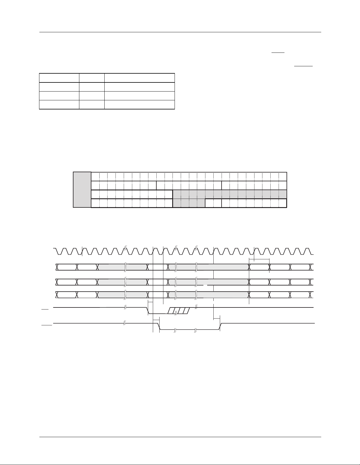
The TMC2192 supports YCBCR component sources on the
pixel data port. YCBCR input sources are supported in 10 bit
4:2:2, 20 bit 4:2:2, 20 bit 4:4:4, and 24 bit 4:4:4. In the 4:2:2
cases the color difference components are linearly interpolated to 4:4:4 internally.
INMODE
23
777
00
01
9
1x
9
C
B
YC C
BR
YC C
BR
15 897
16
0
Figure 1. Input Formats
Demuxing of multiplexed data streams depends on which
synchronization mode the encoder is operating in. For slave
and genlock modes the falling edge of HSIN must be LOW
prior to the CB data in order to demux the data correctly. For
master mode synchronization the falling edge of HSOUT
must be LOW prior to the Y data in order to demux the data
correctly. Finally, in 656 mode the demuxing of the data
stream is determined by the TRS codes, the first sample after
the TRS is considered a C
sample of the CB Y CR YI
B
packet.
The control register D1OFF controls the formatting of the
incoming luminance data at the pixel data port. When
D1OFF is HIGH a blanking level of 64
is subtracted from
10
the luminance and when D1OFF is LOW the incoming the
pixel data is passed through. The inversion of the MSB’s on
the CB and CR components is controlled by the INMODE
control register.
PD 0
C
R
1
0Y90
Y
000
2
2192002A
1. INMODE = 00, PD[7:0] = PD[23:16] = CB, PD[15:8] = C
PXCK
PD[7:0]
PD[23:16]
PD[15:8]
HSIN
HSOUT
(TSOUT = 1)
Y
n-1
C
B
C
n-1
R
Y
n
C
n-1
n
B
C
n
R
Y
0
C
0
B
C
0
R
t
SP
t
DO
Figure 2. 24 Bit Input Format
2. INMODE = 01, PD[23:14] = YCBCR running at 27MHz.
The PD port is clocked at twice the pixel rate, with the data
organized as CB Y CR Y, with the cosited Y's following the
CB's. In its CCIR-656 time base mode, the demuxed CB, Y,
and CR data is synchronized to the SAV preamble. The first
R
t
DO
x = (SY+BR+BU+CBP)*2
t
S
Y
C
B
C
R
t
H
Y
x
x
x
x+1
C
x+1
B
C
x+1
R
Y
x+2
C
x+2
B
C
x+2
R
1280n = (SY+BR+BU+CBP+AV)*2
data value, after the SAV preamble, is treated as a CB data
point in the multiplexed CB, Y, CR Y , D1 data stream.
Note: Figure 3, pixel numbering, reflects the SMPTE-125M
pixel numbering.
2192003A
REV. 1.0.0 8/13/03 7
TMC2192 PRODUCT SPECIFICATION
PXCK
PD[23:14]
Y
C
718
B718
Y
C
719
R718
00
FF
FV
00
EAV
HSOUT
(TSOUT = 1)
n = (SY+BR+BU+CBP+AV)*2
PXCK
PD[23:14]
Y
C
Bn
Y
C
n
n+1
Rn
HSIN
HSOUT
(TSOUT = 1)
3. INMODE = 11, PD[9:0] = Y, PD[23:14] = CB/CR
n = (SY+BR+BU+CBP+AV)*2
PXCK
PD[9:0]
Y
Y
n
n+1
0
C
Y
B736
1
736
t
DO
128
t
t
HS
DO
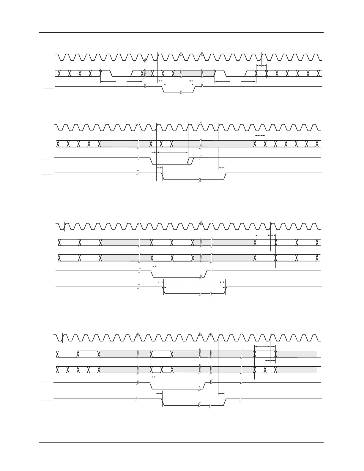
Figure 3. CCIR656 Input Format
0
C
Y
B0
0
t
SP
t
DO
t
HP
Figure 4. 10 bit Input Format
0
Y
0
Y
1
(SY+BR+BU+CBP)*2
t
t
S
H
C
C
FF
00
00
FV
0
Y
B0
0
Y
R0
1
Y
C
2
B2
SAV
65-6294-04
128
t
DO
128
x = (SY+BR+BU+CBP)*2
t
S
C
Bx
x = (SY+BR+BU+CBP)*2
t
S
Y
t
H
Y
C
Y
x
Rx
x+1
t
H
Y
x
x+1
C
Bx+2
65-6294-05
Y
x+2
Y
x+2
PD[23:14]
C
C
Bn
Rn
C
t
SP
C
B0
R0
HSIN
t
HSOUT
(TSOUT = 1)
DO
t
HS
Figure 5. 20 bit 4:2:2 Input Format
4. INMODE = 10, PD[9:0] = Y at PCK, PD[23:14] = CB-CR at PXCK
n = (SY+BR+BU+CBP+AV)*2
PXCK
PD[9:0]
PD[23:14]
C
B
n
HSIN
HSOUT
(TSOUT = 1)
Y
Y
n
n+1
C
C
C
n
n+1
R
B
Rn+1
0
Y
0
C
C
B
0
0
R
t
SP
t
DO
Figure 6. 20 bit 4:4:4 Input Format
C
t
DO
128
x = (SY+BR+BU+CBP)*2
t
S
Y
t
S
C
B
x
t
DO
C
Bx
x
Rx
t
H
t
H
C
x
R
C
Bx+2
65-6294-06
65-6294-07
8 REV. 1.0.0 8/13/03
PRODUCT SPECIFICATION TMC2192
Color Space Matrix
Control Registers for this section
Address Bit(s) Name
0x30 7-0 MCF1L
0x33 7-0 MCF2L
0x35 7-0 MCF3L
0x3A 7-4 MCF1M
0x3B 2-0 MCF2M
0x3C 2-0 MCF3M
Table 1. CSM Coefficient Range
Coefficient Gain Range Comment
MCF1 0 to 2
MCF2 0 to 1 11 bit coefficient.
MCF3 0 to 1 11 bit coefficient.
Matrix configuration:
Y
composite
U = MCF2 * C
V = MCF3 * C
The color space matrix consists of 3 multipliers with independently adjustable coefficients, and a resolution of
0.00049 (1/2048). The amount of gain varies among coefficients, Table 1 summarizes the gain for each coefficient.
= MCF1 * Y
in
B
R
To aid in the programming of the color space matrix Table 2
provides a set of default input and output values for 100%
color bars. The component values given will be after the pre-
Table 2. Expected Output Values for the CSM with YCBCR Inputs
Inputs 5:2 Outputs 7:3 Outputs
Color
White 876 0 0 536 0 0 568 0 0
Yellow 776 -448 73 475 -235 54 503 -249 57
Cyan 614 151 448 376 79 -332 407 84 -351
Green 514 -297 -375 315 -156 -278 340 -165 -294
Magenta 362 297 375 222 156 278 240 165 294
Red 262 -151 448 160 -79 332 173 -84 351
Blue 100 448 -73 61 235 -54 66 249 -57
Black 000000000
Blank 64 240 256
Pedestal 44 0
Sync 8 12
YC
B
C
R
YUVYUV
processing block and prior to the sync and pedestal insertion.
The blank, pedestal, and sync values are given as a reference.
Table 4 gives the default coefficients values for the CSM.
REV. 1.0.0 8/13/03 9
TMC2192 PRODUCT SPECIFICATION
Synchronization Modes
Control Registers for this section
Address Bit(s) Name
0x06 5-3 MODE
0x06 1 TOUT
0x06 0 TSOUT
The TMC2192 offers a variety of synchronization modes;
these are master, slave, genlock, 656 mode, and DRS-Lock.
In master mode, the TMC2192 generates its own timing and
the synchronization is supplied externally by HSOUT and
VSOUT
derives its timing from the input pins HSIN, VSIN. In 656
mode the timing is driven by the synchronization codes
embedded into the data stream.
Master
The TMC2192 drives the output pins HSOUT and VSOUT
to synchronize the incoming video. A new color frame starts
at the rising edge of RESET. The encoder always starts at the
1st vertical serration in field 8 and will freerun the field and
line sequence. The control register bit SRESET can be used
to synchronize the start of the field and line sequence in master mode by resetting the FVHGEN state machine. Output
synchronization signal VSOUT can operate in a traditional
sync mode or in a MPEG style field toggle mode.
Slave
The TMC2192 is driven by the input synchronization pins
HSIN and VSIN. When the falling edge of HSIN and VSIN
occurs at the same rising edge of PXCK the TMC2192 will
start a new field.VSIN can be either a traditional pulse or the
MPEG style field toggle. In both cases the TMC2192 will
flywheel through fields 2, 4, 6, and 8 synchronizing only to
fields 1, 3, 5, and 7.
signals. In slave and genlock modes the TMC2192
CCIR656
The TMC2192 derives all synchronization from the embedded TRS (timing reference signals) information. Blanking of
selected lines is determined by the v bit of the TRS. However
the control registers VBIENx can override and blank the
active video portion of VBI lines regardless of the state of the
v-bit.
Genlock
The TMC2192 is driven by the input synchronization pins
HSIN
and VSIN. When the falling edge of HSIN and VSIN
occurs at the same rising edge of PXCK the TMC2192 will
start a new field.VSIN
can be either a traditional pulse or the
MPEG style field toggle. In both cases the TMC2192 will
flywheel through fields 2, 4, 6, and 8 synchronizing only to
fields 1, 3, 5, and 7. The TMC2192 collects GRS data and
resets its subcarrier phase and frequency to the data embedded in the GRS stream. The GRS detection occurs only on
the CBVS port.
DRS
The TMC2192 is driven by the input synchronization pins
HSIN and VSIN. When the falling edge of HSIN and VSIN
occurs at the same rising edge of PXCK the TMC2192 will
start a new field.VSIN can be either a traditional pulse or the
MPEG style field toggle. In both cases the TMC2192 will
flywheel through fields 2, 4, 6, and 8 synchronizing only to
fields 1, 3, 5, and 7. Subcarrier phase adjustment is determined by the DRS data. The DRS detection can occur on
either the CBVS port or the pixel data port.
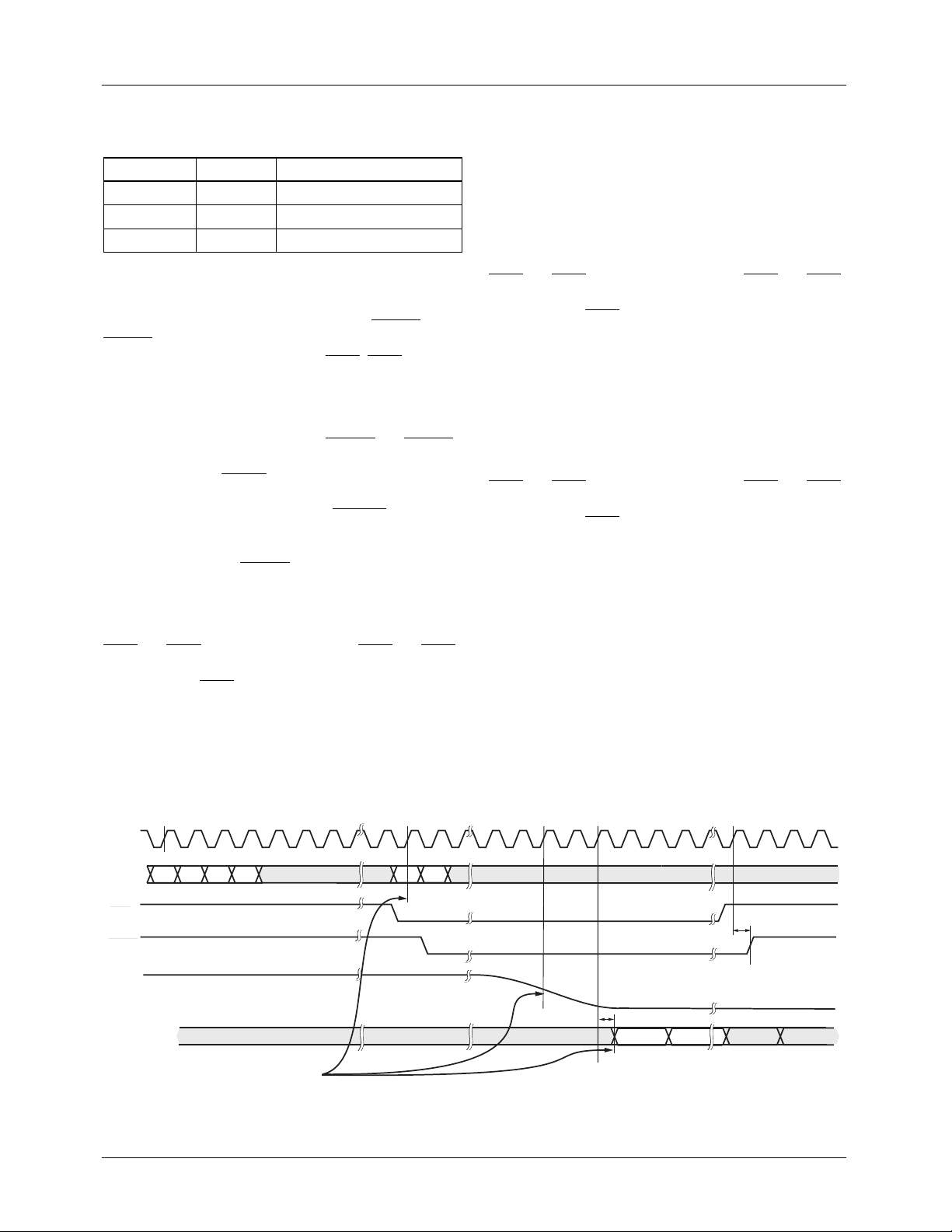
Propagation Delay
The propagation delay from the pixel data (PD) input to the
D/A output is 64 PXCK’s. Figure 8 shows the propagation
delay for both master and slave synchronization modes. For
CCIR656 data streams, pixel 736 (pixel 0 in Figure 8) is the
midpoint of sync and is 32 PXCK’s (24 PXCK’s in PAL)
after the EAV TRS.
n = (SY+BR+BU+CBP+AV)*2
PXCK
C
PD[23:14]
HSIN
HSOUT
(TSOUT = 1)
DACx
(ANALOG)
DCVBS
(D[7:0],FLD[2:1])
Bn
Y
C
n
Y
n+1
Rn
Midpoint of the
Falling Edge of Sync
0
C
Y
B0
0
63 65
t
DO
COMP
0
COMP
128
t
DO
1
65-6294-09
Figure 7. Propagation Delay through the Encoder
10 REV. 1.0.0 8/13/03

PRODUCT SPECIFICATION TMC2192
Blanking Control
Control Registers for this section
Address Bit(s) Name
0x04 1-0 PDRM
0x06 2 PDCDIR
0x18 4-0 VBIENF1
0x19 4-0 VBIENF2
0x1F 7-0 PDCCNT
The content of VBIENFx[4:0] selects the first line to contain
an active video region in each field, all subsequent lines for
the remainder of the field are active. To blank an entire field,
the user zeroes the VBIENFx[4:0] control register. In
CCIR656 slave mode, the user can selectively blank any
enabled line by setting its TRS V bit HIGH. For 525-line
systems, NTSC line numbering is employed, with the first
vertical serration starting on line 4. PAL line numbering is
used with 625-line systems, with each field's line 1 being the
start of the first vertical serration.
Any line(s) enabled by the closed caption control are automatically unblanked for the closed caption waveform, irrespective of the corresponding values of VBIENF.
Pixel Data Control
The pixel data control has two modes of operation, as an
input or as an output. The mode of operation is determined
by the PDCDIR control register. When PDC is an input the
internally generated PDC is ANDed with the PDC pin. This
allows the user to blank any active video regions. When PDC
is an output, the internally generated PDC is the output for
the PDC pin.
The internal PDC control will toggle to a logic HIGH at the
pixel specified by PDCNT and toggle to a logic LOW four
pixels prior to the end of the active video region. The starting
point and ending point of the active video region (VA) are
determined by the control registers 10h to 1Fh. When PDC is
used as an input, the sloped edge of the active video region
will occur on the next four pixels following the toggle point.
Edge Shaping
The TMC2192 has three modes of sloped edges on the active
video region and are controlled by PDRM control register.
Table 3. PDC Edge Control
PDRM[1:0] Slope type at PDC (HIGH) Slope type at PDC (LOW)
00 The following four pixels have the weighting of
1/8, 1/2, 7/8 and 1 for NTSC and 1/8, 3/8, 5/8,
and 7/8 for PAL.
01 The fifth pixel is sampled and scaled 1/8, 1/2,
7/8 and 1 over the next four pixels for NTSC
and 1/8, 3/8, 5/8, and 7/8 over the next four
pixels for PAL.
1x Slope is off, edge control is dictated by the PD
stream from active video start
The following four pixels have the weighting of
1, 7/8, 1/2, and 1/8 for NTSC and 7/8, 5/8, 3/8,
and 1/8 for PAL.
The fifth pixel s sampled and scaled 1, 7/8, 1/2
and 1/8 over the next four pixels for NTSC and
7/8, 5/8, 3/8, and 1/8 over the next four pixels
for PAL.
Slope is off, edge control is dictated by the PD
stream to active video end
REV. 1.0.0 8/13/03 11
TMC2192 PRODUCT SPECIFICATION
Horizontal Programming
Control registers for this section
Address Bit(s) Name
0x06 7-6 FORMAT
0x19 7 SHORT
0x19 6 T512
0x19 5 HALFEN
0x20 7-0 SY
0x21 7-0 BR
0x22 7-0 BU
0x23 7-0 CBP
0x24 7-0 XBP
0x25 7-0 VA
0x26 7-0 VC
0x27 7-0 VB
0x28 7-0 EL
0x29 7-0 EH
0x2A 7-0 SL
0x2B 7-0 SH
0x2C 7-0 FP
0x2D 7-6 XBP (MSB’s)
0x2D 5-4 VA (MSB’s)
0x2D 3-2 VB (MSB’s)
0x2D 1-0 VC (MSB’s)
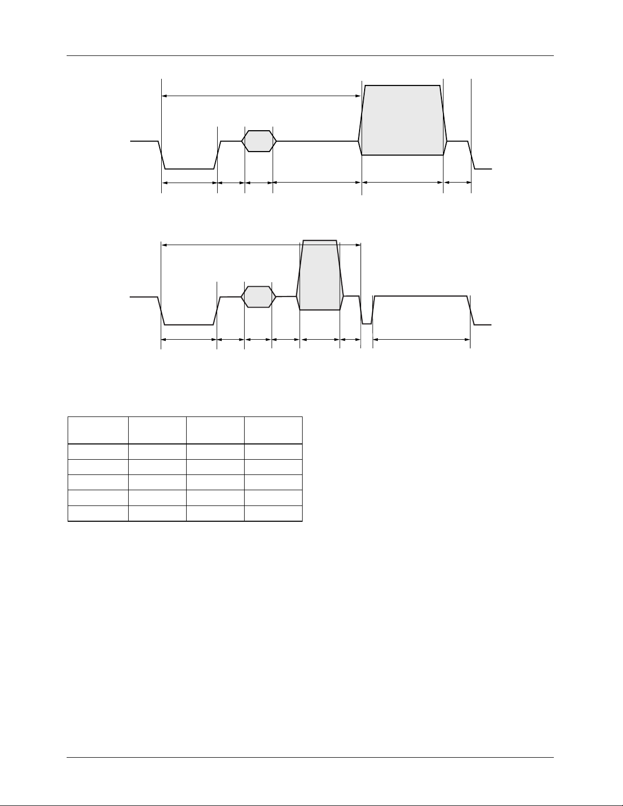
Horizontal interval timing is fully programmable and is
established by loading the timing registers with the duration
of each horizontal element. The duration is expressed in
PCK clock cycles. In this way, any pixel clock rate between
10 MHz and 15 MHz can be accommodated, and any desired
standard or non-standard horizontal video timing may be
produced.
Horizontal timing parameters can be calculated as follows:
t = N x ( PCK period )
= N x ( 2 x PXCK period )
where N is the value loaded into the appropriate timing
register, and PCK is the pixel clock period.
When programming horizontal timing, subtract 5 PCK
periods from the calculated values of CBP and add 5 PCK
periods to the calculated value for VA. The control register
HALFEN
NTSC, PAL-M and line 23 for all other PAL standards when
it is LOW.
enables the 1st half line (UBV) on line 283 for
Table 4. Horizontal Line Equations
Line Type Line ID Line Length Equals
EE 00 EL + EH + EL + EH
SE 02 SL + SH + EL + EH
SS 03 SL + SH + SL + SH
ES 01 EL + EH + SL + SH
EB 10 EL + EH + EL + EH
UBB, -BB 0D, 05 SY + BR + BU + CBP + VA + FP
UVV, -VV 0F, 07 SY + BR + BU + CBP + VA + FP
UVE, -VE 0C, 04 SY + BR + BU + CBP + VC + FP + EL + EH
UBV 0E SY + BR + BU + XBP + VB + FP
12 REV. 1.0.0 8/13/03
PRODUCT SPECIFICATION TMC2192
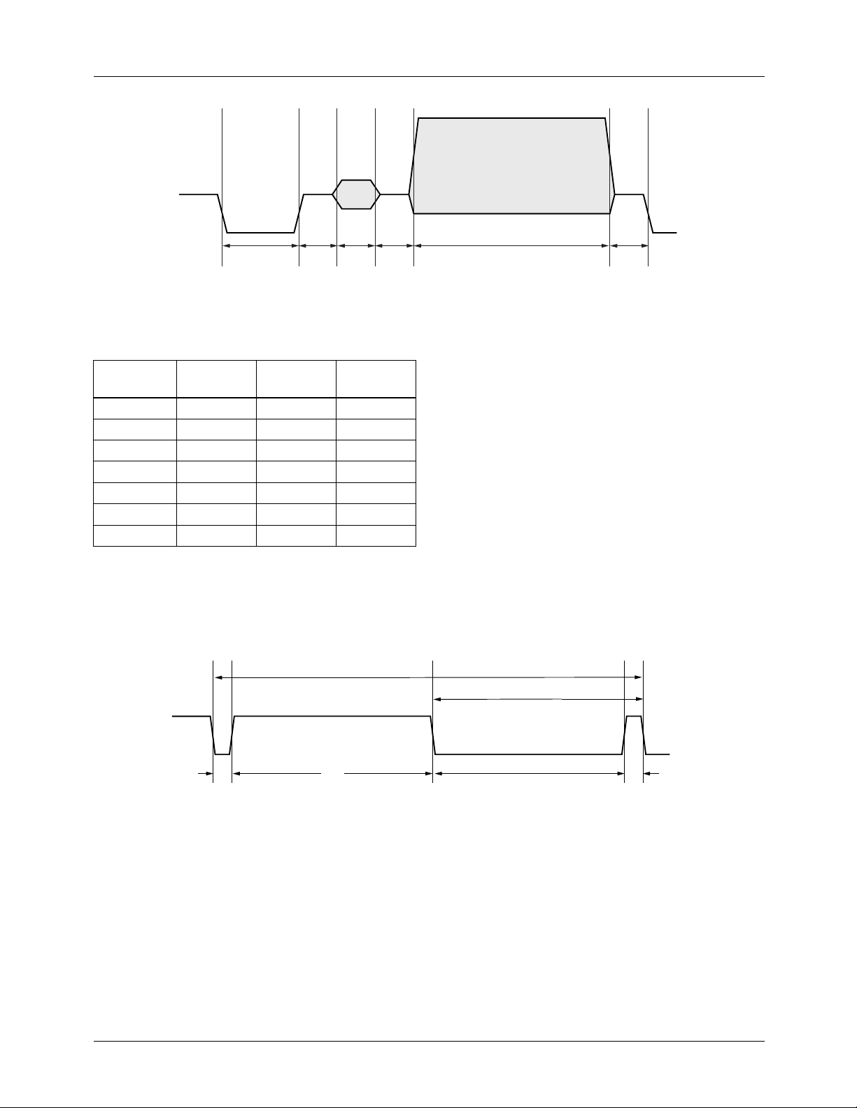
SY
BR BU CBP VA FP
Figure 8. Horizontal Timing
Table 5. Horizontal Timing Specifications
Parameter
NTSC-M
(µs)
PAL-I
(µs)
PAL-M
(µs)
FP 1.5 1.65 1.9
SY 4.7 4.7 4.95
BR 0.6 0.9 0.9
BU 2.5 2.25 2.25
CBP 1.6 2.55 1.8
VA 52.6556 51.95 51.692
H 63.5556 64.0 63.492
Vertical interval timing is also fully programmable, and is
established by loading the timing registers with the duration’s of each vertical timing element, the duration expressed
in PCK clock cycles. In this way as with horizontal program-
65-6294-10
ming, any pixel rate between 10 and 15 Mpps can be accommodated, and any desired standard or non-standard vertical
video timing may be produced.
Like horizontal timing parameters, vertical timing parameters are calculated as follows:
t = N x ( PCK period )
= N x ( 2 x PXCK period )
where N is the value loaded into the appropriate timing register, and PCK is the pixel clock period.
The vertical interval comprises several different line types
based upon H, the Horizontal line time.
H = (2 x SL) + (2 x SH) [Vertical sync pulses]
= (2 x EL) + (2 x EH) [Equalization pulses]
H
H/2
EL
EH SL SH
65-6294-11
Figure 9. Horizontal Timing – Vertical Blanking
The VB and VC control registers are added to produce the
half-lines needed in the vertical interval at the beginning and
end of some fields. These must properly mate with components of the normal lines.
REV. 1.0.0 8/13/03 13
TMC2192 PRODUCT SPECIFICATION
H/2
SY
SY
BR BU XBP
Figure 10. Horizontal Timing – 1st Half-line
BR
Figure 11. Horizontal Timing – 2nd Half-line
Table 6. Vertical Interval Timing Specifications
NTSC-M
Parameter
(µs)
H 63.5556 64 63.492
EH 29.4778 29.65 29.45
EL 2.3 2.35 2.3
SH 4.7 4.7 4.65
SL 27.1 27.3 27.1
PAL-I
(µs)
H/2
BU
CBP VC FP
PAL-M
(µs)
EL
VB FP
65-6924-12
EH
65-6294-13
14 REV. 1.0.0 8/13/03
PRODUCT SPECIFICATION TMC2192
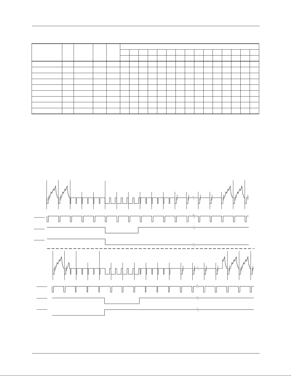
Table 7. Default Horizontal Timing Parameters
Field
Horizontal
Standard
NTSC sqr. pixel 59.94 15.734266 12.27 24.54 3A 07 1F 0F 23 8B 05 77 1C 6A 4C 3A 12 65 52
NTSC CCIR-601 59.94 15.734266 13.50 27.00 40 08 22 11 44 CB 1E 98 1F 8E 6D 40 14 65 59
NTSC 4x F
PAL sqr. pixel 50.00 15.625000 14.75 29.50 45 0D 21 21 6D 03 2B B7 23 B5 93 45 19 75 61
PAL CCIR-601 50.00 15.625000 13.50 27.00 40 0C 1E 22 4D BE 0E 93 20 90 70 40 16 65 59
PAL 15 Mpps 50.00 15.625000 15.00 30.00 46 0D 22 21 73 11 31 BF 23 BD 9A 47 19 75 62
PAL-M sqr.pixel 60.00 15.750000 12.50 25.01 3E 0B 1C 13 26 86 FE 8B 1D 70 53 3A 18 61 52
PAL-M CCIR-601 60.00 15,750000 13.50 27.00 44 0C 1E 13 26 Bf 12 99 1F 8E 6E 3F 1A 65 57
PAL-M 4x F
SC
Rate
(Hz)
59.94 15.734266 14.32 28.64 43 09 24 12 54 F7 30 B5 21 A6 84 43 15 65 5F
60.00 15,750000 14.30 28.60 47 0D 20 15 4C E8 22 AC 21 A5 84 42 1B 65 5D
SC
Freq.
(KHz)
Pixel
Rate
(Mpps)
PXCK
SY BR BU CBP XBP VA VC VB EL EH
Freq.
20 21 22 23 24 25 26 27 28 29 2A 2B 2C 2D 2F
(MHz)
Timing Register (hex)
2SL2
SH FP Note CBL
Notes:
1. XBP, VA, VC, and VB are 10 bit values. The 2 MSBs for these four variables are in Timing Register 2D.
2. EH and SL are 9 bit values. A most significant "1" is forced by the TMC2192 since EH and SL must range from 256 to 511.
EH and SL may be extended to 767. Only the eight LSBs are stored in Timing Registers 29 and 2A.
3. Every calculated timing parameter has a minimum value of 5 except EH and SL which have minimum values of 256.
Vertical Timing
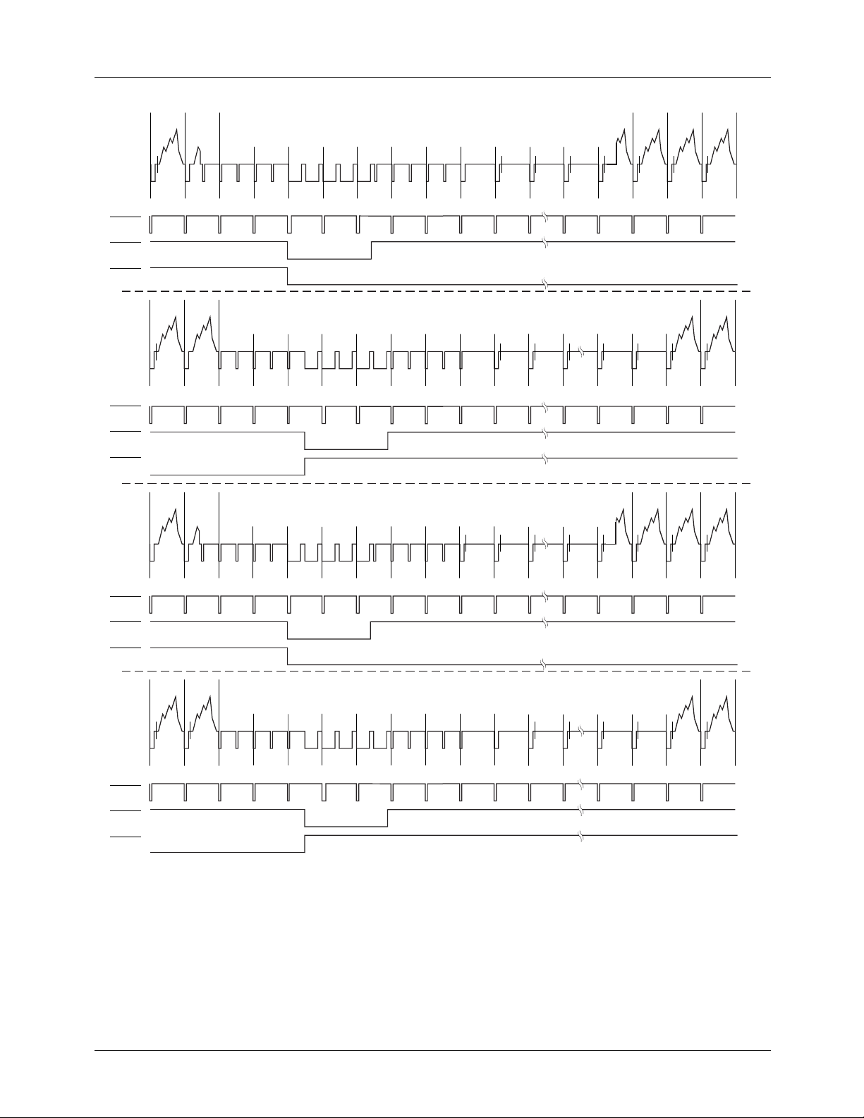
The vertical timing is controlled by the FORMAT control
register, which dictates the field and line sequence.
524
525
FIELDS 1 AND 3
22
HSOUT
VSOUT
(TOUT = 1)
VSOUT
(TOUT = 0)
HSOUT
VSOUT
(TOUT = 1)
VSOUT
(TOUT = 0)
UVV
UVVEEEEEEEEESEESSSSSSSSSESSEEEEEEEEEBEE
262
UVV
263
26412652266326742685269627072718272
UVE
FIELDS 2 AND 4
Figure 12. NTSC Vertical Interval
•••
9
UBB
27310•••
UBB
19
UBB
UBB
282
UBB
UVV
UVV
2832028421285
UVV
UBV
UVV
65-6294-15
REV. 1.0.0 8/13/03 15
TMC2192 PRODUCT SPECIFICATION
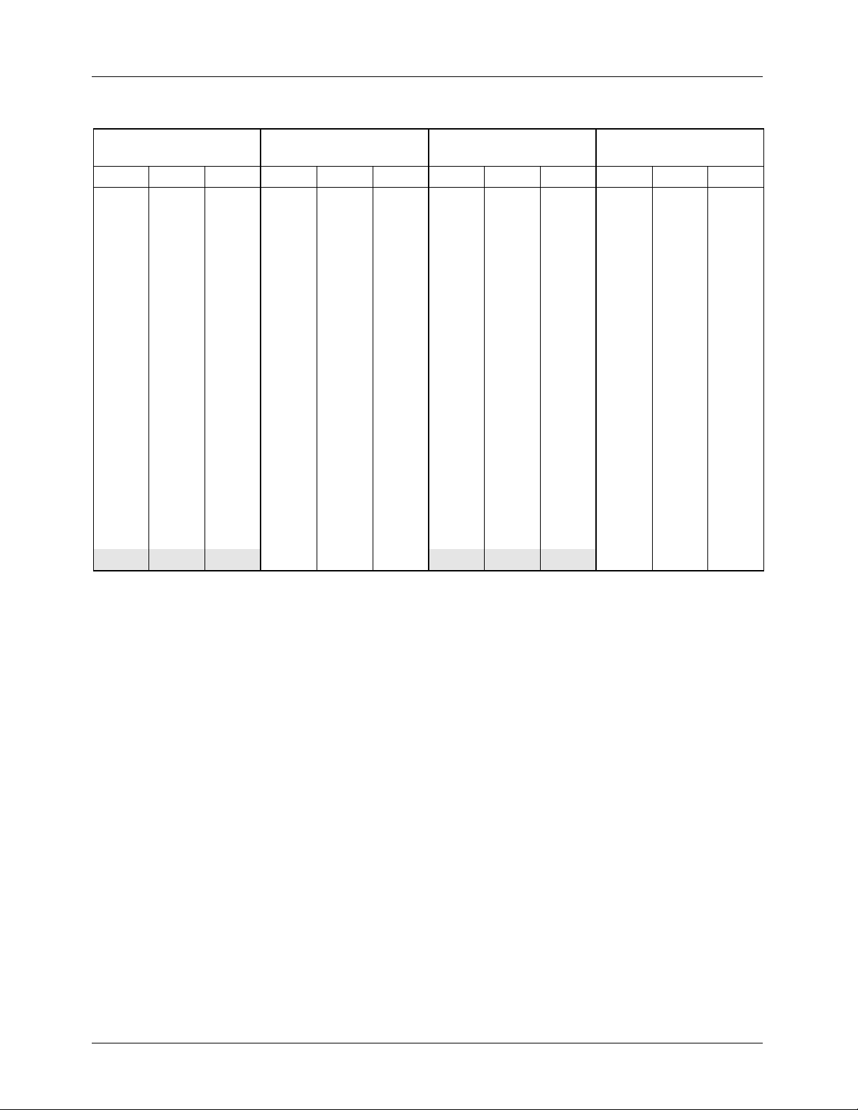
Table 8. NTSC Field/Line Sequence and Identification
Field 1
FIELD ID = x00
Line ID LTYPE Line ID LTYPE Line ID LTYPE Line ID LTYPE
4 SS 03 266 ES 01 4 SS 03 266 ES 01
5 SS 03 267 SS 03 5 SS 03 267 SS 03
6 SS 03 268 SS 03 6 SS 03 268 SS 03
7 EE 00 269 SE 02 7 EE 00 269 SE 02
8 EE 00 270 EE 00 8 EE 00 270 EE 00
9 EE 00 271 EE 00 9 EE 00 271 EE 00
10 UBB 0D 272 EB 10 10 UBB 0D 272 EB 10
… UBB 0D 273 UBB 0D … UBB 0D 273 UBB 0D
19 UBB 0D … UBB 0D 19 UBB 0D … UBB 0D
20 UBB 0D 282 UBB 0D 20 UBB 0D 282 UBB 0D
21 UVV 0F 283 UBV 0E 21 UVV 0F 283 UBV 0E
22 UVV 0F 284 UVV 0F 22 UVV 0F 284 UVV 0F
… UVV 0F … UVV 0F … UVV 0F … UVV 0F
262 UVV 0F 524 UVV 0F 262 UVV 0F 524 UVV 0F.
263 UVE 0C 525 UVV 0F 263 UVE 0C 525 UVV 0F
264 EE 00 1 EE 00 264 EE 00 1 EE 00
265 EE 00 2 EE 00 265 EE 00 2 EE 00
Field 2
FIELD ID = x01
3EE00 3EE00
FIELD ID = x10
Field 3
Field 4
FIELD ID = x11
EE Equalization pulse
SE Half-line vertical sync pulse, half-line equalization pulse
SS Vertical sync pulse
ES Half-line equalization pulse, half-line vertical sync pulse
EB Equalization broad pulse
UBB Black burst
UVV Active video
UVE Half-line video, half-line equalization pulse
UBV half-line black, half-line video
16 REV. 1.0.0 8/13/03
PRODUCT SPECIFICATION TMC2192
HSOUT
VSOUT
(TOUT = 1)
VSOUT
(TOUT = 0)
HSOUT
VSOUT
(TOUT = 1)
VSOUT
(TOUT = 0)
623
622
UVV
309 310
UVV
623
622
FIELDS 1 AND 5
624 625 1
-VE EE EE SS SS SE EE EE -BB
FIELDS 2 AND 6
311 312 313
-VV EE EE ES SS SS EE EE EB
FIELDS 3 AND 7
23
314 315
45 67
UBB
316 317 318 319
UBB
•••
•••
320
23
24
22
UBVUBB UVV UVV
UVV
•••
334 335
•••
UBBUBB UVV UVV
UBB
23
24
25 26
336 337
25 26
HSOUT
VSOUT
(TOUT = 1)
VSOUT
(TOUT = 0)
HSOUT
VSOUT
(TOUT = 1)
VSOUT
(TOUT = 0)
624 625 1
-VV -VE EE EE SS SS SE EE EE UBB UBB
309 310
UVV
UVV EE EE ES SS SS EE EE EB
FIELDS 4 AND 8
311 312 313 314 315 316 317
23
45 67
318
319
-BB
Figure 13. PAL Vertical Interval
•••
22
•••
320 334 335
UBVUBB UVV UVV
UVV
•••
•••
UBBUBB UVV UVV
UBB
336 337
65-6294-16
REV. 1.0.0 8/13/03 17

TMC2192 PRODUCT SPECIFICATION
Table 9. PAL Field/Line Sequence and Identification
Field 1 & 5
FIELD ID = 000, 100
Field 2 & 6
FIELD ID = 001, 111
Field 3 & 7
FIELD ID = 010, 110
Field 4 & 8
FIELD ID = 011, 111
Line ID LTYPE Line ID LTYPE Line ID LTYPE Line ID LTYPE
1 SS 03 313 ES 01 1 SS 03 313 ES 01
2 SS 03 314 SS 03 2 SS 03 314 SS 03
3 SE 02 315 SS 03 3 SE 02 315 SS 03
4 EE 00 316 EE 00 4 EE 00 316 EE 00
5 EE 00 317 EE 00 5 EE 00 317 EE 00
6 -BB 05 318 EB 10 6 UBB 0D 318 EB 10
7 UBB 0D 319 UBB 0D 7 UBB 0D 319 -BB 05
… UBB 0D 320 UBB 0D … UBB 0D 320 UBB 0D
22 UBB 0D … UBB 0D 22 UBB 0D … UBB 0D
23 UBV 0E 334 UBB 0D 23 UBV 0E 334 UBB 0D
24 UVV 0F 335 UBB 0D 24 UVV 0F 335 UVV 0F.
25 UVV 0F 336 UVV 0F 25 UVV 0F 336 UVV 0F
26 UVV 0F 337 UVV 0F 26 UVV 0F 337 UVV 0F
… UVV 0F … UVV 0F … UVV 0F … UVV 0F
309 UVV 0F 622 -VV 07 309 UVV 0F 622 UVV 0F
310 -VV 07 623 -VE 04 310 UVV 0F 623 -VE 04
311 EE 00 624 EE 00 311 EE 00 624 EE 00
312 EE 00 625 EE 00 312 EE 00 625 EE 00
EE Equalization pulse
SE Half-line vertical sync pulse, half-line equalization pulse
SS Vertical sync pulse
ES Half-line equalization pulse, half-line vertical sync pulse
EB Equalization broad pulse
UBB Black burst
-BB Black burst with color burst suppressed
UVV Active video
-VV Active video with color burst suppressed
UVE Half-line video, half-line equalization pulse
-VE Half-line video, half-line equalization pulse, color burst suppressed.
UBV half-line black, half-line video
18 REV. 1.0.0 8/13/03
PRODUCT SPECIFICATION TMC2192
HSOUT
VSOUT
(TOUT = 1)
VSOUT
(TOUT = 0)
HSOUT
VSOUT
(TOUT = 1)
VSOUT
(TOUT = 0)
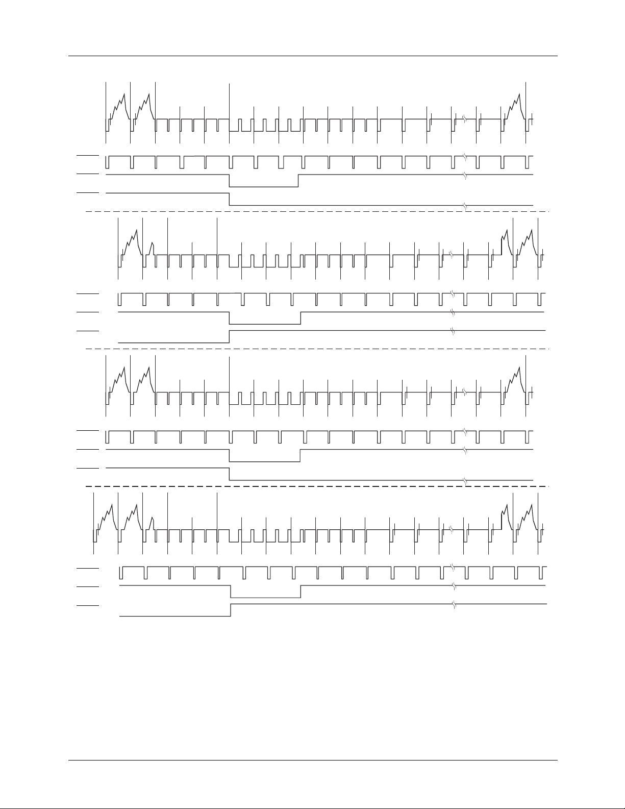
521 522 FIELDS 1 AND 5
523524525123456
UVV UVV EE EE EE SS SS SS EE EE EE
260 FIELDS 2 AND 6
259
261 262 263 264 265 266 267 268 269
UVV-VEEEEEESSSSSSEEEEEEB
521 522 FIELDS 3 AND 7
523524525123456
18
789•••
-BB UBB-BB UBB UVV
270 •••
271 279
-BB UBB UBB UBV UVV
789•••
•••
17
•••
280 281
18
17
HSOUT
VSOUT
(TOUT = 1)
VSOUT
(TOUT = 0)
HSOUT
VSOUT
(TOUT = 1)
VSOUT
(TOUT = 0)
UVV-VVEEEEEESSSSSSEEEEEE
260 FIELDS 4 AND 8
259258
261 262 263 264 265 266 267 268 269 270 •••
-VVUVV -VEEEEEESSSSSSEEEEEEB
Figure 14. PAL-M Vertical Interval
-BB UBBUBB UBB UVV
271 279
UBB UBB UBB UBV UVV
•••
280 281
•••
65-6294-17
REV. 1.0.0 8/13/03 19

TMC2192 PRODUCT SPECIFICATION
Table 10. PAL-M Field/Line Sequence and Identification
Field 1 & 5
FIELD ID = 000, 100
Field 2 & 6
FIELD ID = 001, 111
Field 3 & 7
FIELD ID = 010, 110
Field 4 & 8
FIELD ID = 011, 111
Line ID LTYPE Line ID LTYPE Line ID LTYPE Line ID LTYPE
1 SS 03 263 ES 01 1 SS 03 263 ES 01
2 SS 03 264 SS 03 2 SS 03 264 SS 03
3 SS 03 265 SS 03 3 SS 03 265 SS 03
4 EE 00 266 SE 02 4 EE 00 266 SE 02
5 EE 00 267 EE 00 5 EE 00 267 EE 00
6 EE 00 268 EE 00 6 EE 00 268 EE 00
7 -BB 05 269 EB 10 7 -BB 05 269 EB 10
8 -BB 05 270 -BB 05 8 UBB 05 270 UBB 05
9 UBB 0D 271 UBB 1D 9 UBB 0D 271 UBB 1D
………………………………
17 UBB 0D 279 UBB 0D 17 UBB 0D 279 UBB 0D
18 UVV 0F 280 UBV 0E. 18 UVV 0F 280 UBV 0E.
………281 UVV 0F … UVV 0F 281 UVV 0F
259 UVV 0F ………258 UVV 0F ………
260 -VE 04 521 UVV 0F 259 -VV 07 521 UVV 0F
261 EE 00 522 -VV 07 260 -VE 04 522 UVV 0F
262 EE 00 523 EE 00. 261 EE 00 523 EE 00
524 EE 00 262 EE 00 524 EE 00
525 EE 00 525 EE 00
EE Equalization pulse
SE Half-line vertical sync pulse, half-line equalization pulse
SS Vertical sync pulse
ES Half-line equalization pulse, half-line vertical sync pulse
EB Equalization broad pulse
UBB Black burst
-BB Black burst with color burst suppressed
UVV Active video
-VV Active video with color burst suppressed
UVE Half-line video, half-line equalization pulse
-VE Half-line video, half-line equalization pulse, color burst suppressed.
UBV half-line black, half-line video
20 REV. 1.0.0 8/13/03

PRODUCT SPECIFICATION TMC2192
Chrominance Processor
Control registers for this section:
Address Bit(s) Name
0x06 7-6 FORMAT
0x06 5-3 MODE
0x07 5 DDSRST
0x11 7 DRSSEL
0x18 6 GLKCTL1
0x18 5 GLKCTL0
0x3F 3 GAUSS_BYP
0x40 7-0 FREQL
0x41 7-0 FREQ3
0x42 7-0 FREQ2
0x43 7-0 FREQM
0x44 7-4 SYSPHL
0x45 3-0 SYSPHM
0x46 7-4 BURPHL
0x47 3-0 BURPHM
0x48 7-4 BRSTFULL
0x49 3-0 BRST1
0x4A 7-4 BRST2
Subcarrier Programming
The color subcarrier is produced by an internal 32 bit digital
frequency synthesizer which is completely programmable in
frequency and phase. Separate registers, FREQx, SYSPHx,
BSTPHx, are provided for phase adjustment of the color
burst and of the active video, permitting external delay compensation, color adjustment, etc. FREQx is the subcarrier
phase step per pixel and SYSPHx is phase offset at field 1,
line 1 (line 4 for NTSC), pixel 1.
NTSC Subcarrier
For NTSC encoding, the subcarrier synthesizer frequency
has a simple relationship to the pixel clock period, repeating
over 2 lines: The decimal value for the subcarrier phase step
is:
455 2⁄
FREQx
Where the number of pixels/line is:
pixels line⁄
This value must be converted to binary and split into four 8
bit registers, FREQM, FREQ2, FREQ3, and FREQL.
PAL Subcarrier
The PAL relationship is more complex, repeating only once
in 8 fields (the well-known 25 Hz offset):
FREQx
This value must be converted to binary and split as described
previously for NTSC. The number of pixels/line is found as
in NTSC.
PAL-M Subcarrier
FREQ
SYSPHx establishes the appropriate phase relationship
between the internal synthesizer and the chroma modulator.
The nominal value for SYSPHx is zero.
Other values for SYSPHx must be converted to binary and
split into two 8 bit registers, SYSPHM and SYSPHL.
Burst Phase (BURPHx) sets up the correct relative NTSC
modulation angle. The value for BURPH is:
--------------------------pixels line⁄
PXCK Frequency
------------------------------------------=
1135 4⁄()1 625⁄()+
--------------------------------------------------pixels line⁄
909 4⁄
--------------------------pixels line⁄
232×=
H Period
232×=
32
×=
2
BURPHx = SYSPHx
This value must be converted to binary and split into two 8
bit registers, BURPHM and BURPHL.
REV. 1.0.0 8/13/03 21
 Loading...