

Fairchild Semiconductor TMC1203X40 Datasheet
www.fairchildsemi.com
Features
• 8-bit resolution
• 50 Msps conversion rate
• Low power: 100mW per channel @ 20 Msps
• Integral track/hold
• Independent clock inputs
• Integral and differential linearity error 0.5 LSB
• Differential phase 0.7 degree
• Differential gain 1.8%
• Single +5V power supply
• Three-state TTL/CMOS-compatible outputs
• Low cost
Applications
• Video digitizing (composite and Y-C)
• VGA and CCD digitizing
• LCD projection panels
• Image scanners
• Personal computer video boards
• Multimedia systems
• Low cost, high speed data conversion
• Digital communications
Description
Incorporated into the TMC1203 are three analog-to-digital
(A/D) converters, each with independent clocks and reference voltages. Analog signals are converted to Triple 8-bit
digital words at sample rates up to 50 Msps (Megasamples
per second) per channel.
Integral Track/Hold circuits deliver excellent performance
on signals with full-scale spectral components up to
12 MHz. Innovative two-step architecture conversion
architecture and submicron CMOS technology reduce typical power dissipation to 100 mW per converter.
Power is derived from a single +5 Volt power supply. Outputs are three-state outputs and TTL/CMOS-compatible.
TMC1203 package is a 80-lead Metric Quad Flat Pack
(MQFP). Performance specifications are guaranteed from
0°C to 70°C.
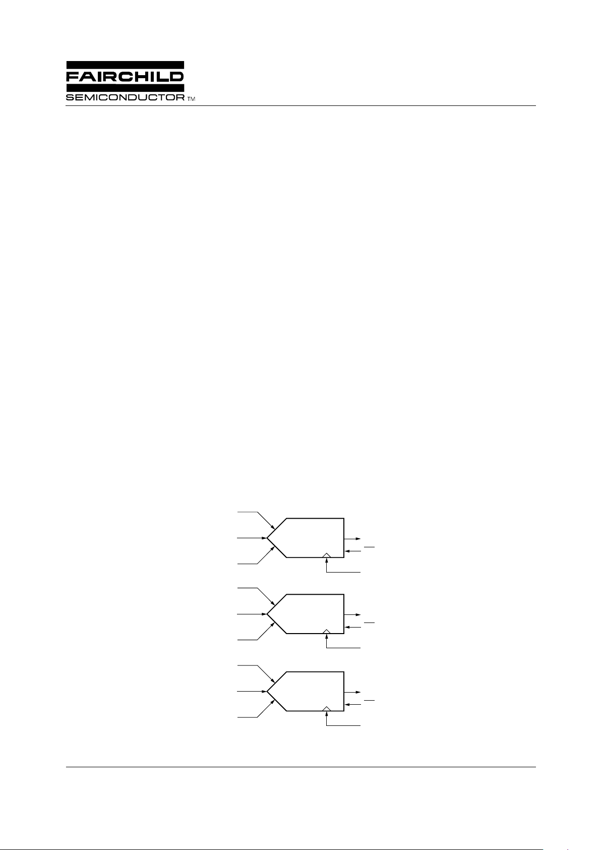
Block Diagram
8-bit
A/D Converter
R
TA
DA
7-0
OE
A
CLK
A
V
INA
R
BA
8-bit
A/D Converter
R
TB
DB
7-0
OE
B
CLK
B
65-3720-01
V
INB
R
BB
8-bit
A/D Converter
R
TC
DA
7-0
OE
C
CLK
C
V
INC
R
BC
TMC1203
Triple Video A/D Converter
8-Bit, 50Msps
Rev. 1.2.0

TMC1203 PRODUCT SPECIFICATION
2
Circuit Function
Within the TMC1203 are three 8-bit A/D converters, each
employing two-step architecture to convert an analog input
to a digital output at rates up to 50 Msps. Input signals are
held in integral track/hold stages during the conversion process. Operation is pipelined, with one input sample taken and
one output word provided for each CLK
X
cycle.
Each of the three converters function identically. In the following descriptions ‘X’ refers to a generic input/output or
clock where ‘X’ is equivalent to A, B or C.
The first step in the conversion process is a coarse 4-bit
quantization. This determines the range of the subsequent
fine 4-bit quantization step. To eliminate spurious codes, the
fine 4-bit A/D quantizer output is gray-coded and converted
to binary before it is combined with the coarse result to form
a complete 8-bit result.
Analog Input and Voltage References
Each A/D accepts analog signals in the range R
BX
to R
TX
into
digital data. Input signals outside this range produce “saturated” 00h or FFh output codes. The device will not
be damaged by signals within the range A
GND
to V
DDA
.
Input range is very flexible and extends from the +5 Volt
power supply to ground. Nominal input range is 2 Volts,
extending from 0.6V to 2.6V. Characterization and
performance is specified over this range. However, the
part will function with a full-scale range from 1.0V to 5.0V.
A smaller input range may simplify analog signal conditioning circuitry, at the expense of additional noise sensitivity
and some reduced differential linearity performance.
External voltage reference sources are connected to the R
TX
and R
BX
pins. R
BX
can be grounded. Within each A/D converter is a reference resistor ladder comprising 255 resistors
that are accessed by the TMC1203 comparators. R
TX
is con-
nected to the top of the ladder, R
BX
to the bottom. Gain and
offset errors are directly related to the accuracy and stability
of the applied reference voltages.
Because a two-step conversion process is employed, it is
important that the references remain stable during the
ENTIRE conversion process (two clock cycles). The reference voltage can then be changed, but any conversion in
progress during a reference change is invalid.
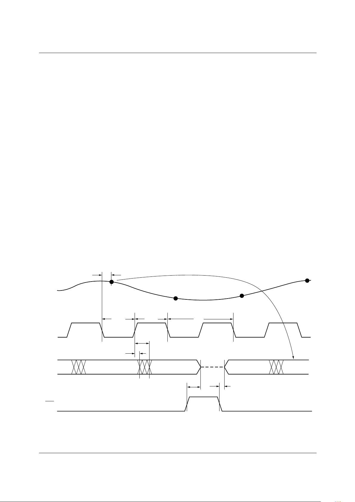
Digital Inputs and Outputs
Sampling of the applied input signal occurs on the "falling"
edge of the CLK
X
signal (Figure 1). Output data is delayed
by 2 1/2 CLK
X
cycles and is valid following the "rising"
edge of CLK
X
. Previous output data remains valid for t
HO
(Output Hold Time), satisfying any hold time requirement of
the receiving circuit. New data becomes valid t
D
(Output
Delay Time) after this rising edge of CLK
X
.
Whenever the analog input signal is sampled and found to be
at a level beyond the A/D conversion range, the output limits
at 00h or FFh, as appropriate.
Table 1. A/D Output Coding
Note: 1 LSB = (R
TX
- R
BX
) / 255
The outputs of the TMC1203 are CMOS- and
TTL-compatible, and are capable of driving four low-power
Schottky TTL loads. An Output Enable control, OE
X
, places
the A/D outputs in a high-impedance state when HIGH.
The outputs are enabled when OE
X
is LOW.
Power and Ground
The TMC1203 operates from a single +5 Volt power supply.
For optimum performance, it is recommended that A
GND
and D
GND
pins of the TMC1203 be connected to the system
analog ground plane.
Input V oltage Output
R
TX
+ 1 LSB FF
R
TX
FF
R
TX
- 1 LSB FE
• • • • • •
R
BX
+ 128 LSB 80
R
BX
+ 127 LSB 7F
• • • • • •
R
BX
+ 1 LSB 01
R
BX
00
R
BX
- 1 LSB 00
PRODUCT SPECIFICATION TMC1203
3
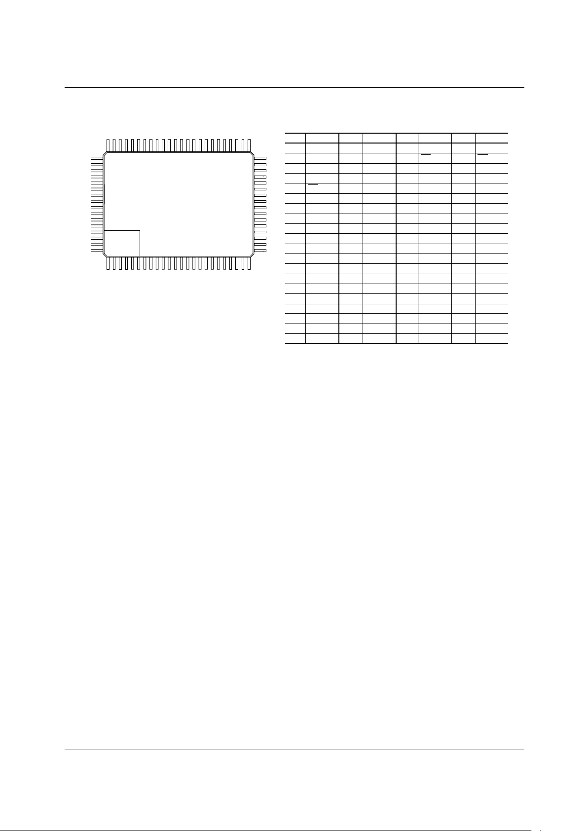
Pin Assignments
NC
DA
5
DA
6
DA
7
OE
A
V
DD
V
DD
NC
CLK
A
NC
V
DDA
V
INA
AGND
R
TA
R
BA
DGND
DGND
DGND
DGND
DGND
1
2
3
4
5
6
7
8
9
10
11
12
13
14
15
16
17
18
19
20
DGND
DGND
NC
NC
DGND
DGND
V
DD
V
DD
V
DD
V
DD
NC
DGND
DGND
DC
0
DC
1
DC
2
DC
3
DC
4
DC
5
DC
6
21
22
23
24
25
26
27
28
29
30
31
32
33
34
35
36
37
38
39
40
Pin Name Pin Name
DC
7
OE
C
V
DD
V
DD
CLK
C
NC
V
DDA
V
INC
AGND
R
TC
R
BC
R
BB
R
TB
AGND
V
INB
V
DDA
NC
CLK
B
NC
V
DD
41
42
43
44
45
46
47
48
49
50
51
52
53
54
55
56
57
58
59
60
V
DD
OE
B
DB
7
DB
6
DB
5
DB
4
DB
3
DB
2
DB
1
DB
0
DGND
DGND
NC
DGND
DGND
DA
0
DA
1
DA
2
DA
3
DA
4
61
62
63
64
65
66
67
68
69
70
71
72
73
74
75
76
77
78
79
80
Pin Name Pin Name
124
65-3720-08
25
40
4164
65
80

PRODUCT SPECIFICATION TMC1203
4
Pin Descriptions
Pin Name Pin Number Value Pin Function Description
A/D Converters
V
INA
, V
INB
,
V
INC
12, 55, 48 R
TX
to
R
BX
Analog Inputs. The input voltage conversion range lies between the
voltage applied to the R
TX
and R
BX
pins. R
TX
, R
BX
.
R
TA
, R
TB
, R
TC
14, 53, 50 2.6V Reference Voltage, Top Inputs. DC voltages applied to R
TA
, R
TB
and R
TC
define highest value of V
INX
.
R
BA
, R
BB
, R
BC
15, 52, 51 0.6V Reference Voltage, Bottom Inputs. DC voltages applied to R
BA
,
R
BB
and R
BC
define highest value of V
INX
.
CLK
A
, CLK
B
,
CLK
C
9, 58, 45 CMOS Convert (Clock) Inputs. A/D converter clock inputs. CMOS-
compatible. V
INX
is sampled on the falling edge of CLK
X
. Clock
inputs are separate for the three converters.
DA
7-0
4, 3, 2, 80, 79,
78, 77, 76
CMOS/
TTL
Data outputs, Converter A (D
7
= MSB). Eight-bit CMOS- and
TTL-compatible digital outputs. Valid data is output on the rising
edge of CLK
X
.
DB
7-0
63, 64, 65, 66,
67, 68, 69, 70
CMOS/
TTL
Data outputs, Converter B (D
7
= MSB). Eight-bit CMOS- and
TTL-compatible digital outputs. Valid data is output on the rising
edge of CLK
X
.
DC
7-0
41, 40, 39, 38,
37, 36, 35, 34
CMOS/
TTL
Data outputs, Converter C (D
7
= MSB). Eight-bit CMOS- and
TTL-compatible digital outputs. Valid data is output on the rising
edge of CLK
X
.
OE
A
, OE
B
, OE
C
5, 62, 42 CMOS Output Enable Inputs. CMOS-compatible. When LOW, the A/D
output is enabled. When HIGH, the output is in a high-impedance
state. Output Enables are separate for the three converters.
Power
V
DDA
11, 47, 56 +5V Analog Supply Voltage. +5 Volt power inputs. These should come
from the same power source and be decoupled to A
GND
.
V
DD
6, 7, 27, 28, 29,
30, 43, 44, 60,
61
+5V Digital Supply Voltage. +5 Volt power inputs. These should come
from the same power source and be decoupled to A
GND
.
A
GND
13, 49, 54 0.0V Analog Ground. Ground connections. These pins should be
connected to the system analog ground plane.
D
GND
16, 17, 18, 19,
20, 21, 22, 25,
26, 32, 33, 71,
72, 74, 75
0.0V Digital Ground. Ground connections. These pins should be
connected to the system analog ground plane.
No Connect
N/C 1, 8, 10, 23, 24,
31, 46, 57, 59,
73
open Not Connected.
PRODUCT SPECIFICATION TMC1203
5
Specification Notes
Bandwidth
Bandwidth specification of an A/D converter is somewhat
different from the normal frequency-response specification
used in amplifiers and filters. An understanding of the differences will help in selecting converters properly for particular
applications.
A/D conversion comprises two distinct processes: sampling
and quantizing. Sampling is grabbing a snapshot of the input
signal and holding it steady for quantizing. The quantizing
process is approximating the analog input to its nearest
numerical value within the conversion range. While
sampling is a high-frequency process, quantizing operates on
a dc signal, held steady by the track/hold circuit. Therefore,
the sampling process relates to the dynamic characteristics of
an A/D converter.
Sampling involves an aperture time, the time needed for the
track/hold circuit to capture the input signal and settle on a
dc value to hold. It is analogous to the shutter speed of a
camera: the shorter the A/D aperture (or faster the shutter)
the less the signal (or picture) will be blurred, and the less
uncertainty there will be in the quantized value. This is not to
be confused with the camera lens opening (aperture), which
is entirely different.
For example, a 10 MHz sinewave with a 1V peak amplitude
(2Vp-p) has a maximum slew rate of 2pfA at zero crossing,
or 62.8V/ms. With an 8-bit A/D converter, q (the quantiza-
tion step size) = 2V/255 = 7.8mV. The input signal will slew
one LSB in 124ps. T o limit the error (and noise) contrib ution
due to aperture effects to 1/2LSB, the aperture must be
shorter than 62ps.
This is the primary reason that the signal to noise ratio drops
off as full scale frequency increases. Notice that the slew rate
is directly proportional to signal amplitude, A. A/Ds will
handle lower-amplitude signals of higher bandwidth, but
other distortion effects will be worsened.
All this is of particular interest in applications such as digitizing analog VGA RGB signals, or the output of a CCD
imaging chip. These data are effectively pre-sampled: there
is a period of rapid slewing from one pixel value to another,
followed by a relatively stable dc level before the signal
slews to the next pixel value. The goal is, of course, to sample on these stable pixel values, not on the slewing between
pixels. During the aperture time, the A/D sees essentially a
dc signal, and bandwidth considerations are less important.
As long as the input circuit can slew and settle to the new
value in the prescribed period, an accurate conv ersion will be
made.
The TMC1203 is capable of slewing a full 2V and settling
between samples taken as little as 25ns apart, making it ideal
for digitizing analog VGA and CCD outputs.
Figure 1. Timing
V
INX
Sample N
Sample N+1
Data N-3 Data N-2 Data N-1 Data N
Hi-Z
Sample N+2
Sample N+3
t
STD
t
PWL
t
PWH
t
DIS
t
ENA
t
DO
t
HO
1/f
S
CLK
X
65-3720-02
DX
7-0
OE
X
 Loading...