Fairchild Semiconductor TMB22153AMS101 Datasheet

TMB22153AMS100
Demonstration Board for the TMC22x5yA
Multistandard Digital Video Decoder
Preliminary Information
www.fairchildsemi.com
Features
• Accepts analog composite or YC
• Outputs 10-bit digital RGB, D1, or YCBC
R
• Locks to studio reference
• R-bus serial interface compatibility
• Raytheon demo board compatibility
Applications
• Evaluation of TMC22x5yA Digital Video Decoder
• Input for Genesis 10-bit Line Doubler board
• Input for DAC and encoder demo boards
• System Breadboarding
Related Products
• TMC2069P7C DAC demonstration board
• TMC2074P7C Encoder demonstration board
• TMB2193MS100 Encoder demonstration board
• TMC2070P7C R-bus interface board
• Raydemo software
Description
The TMB22153AMS100 Demonstration Board showcases
the TMC22x5yA Digital Video Decoder. The onboard MMC
FE-100 dual 10-bit A/D modules generate digitized composite or YC for the decoder. The decoder outputs D1, digital
RGB, or YCBCR. Clocks and synchronization pulses are generated by Fairchild’s TMC2072 Genlocking Video Digitizer.
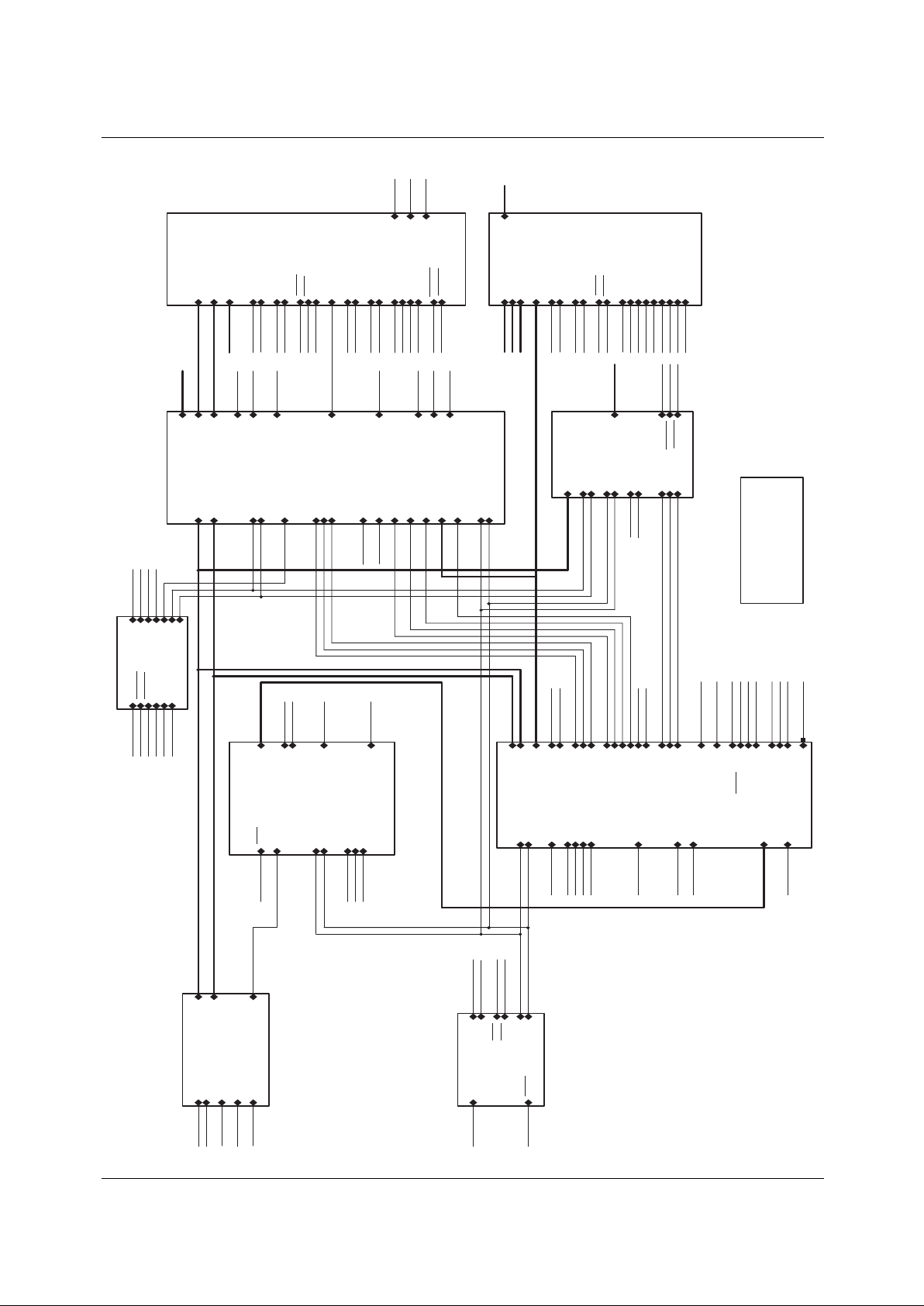
Block Diagram
FE-100x-1
FE-100x-2
Framestore
Connector
RBUS
TMC22153A
TMC2072
SW1
D.C. supply
Analog signals
Composite/Luma
video input
Y/C video input
Chroma
video input
Digital signals
TMB22153AMS100
96 way Edge
Connector (male)
10 bit G/Y
10 bit B/U
10 bit R/V or D1
PXCK clock
HSYNC
VSYNC
SYNC\ (D/A signals)
BLANK\ (D/A signals)
Micro (top)
FPGA (bottom)
PRELIMINARY INFORMATION describes products that are not in full production at the time of printing. Specifications are based on design goals
and limited characterization. They may change without notice. Contact Fairchild Semiconductor for current information.
Rev. 001

TMB22153AMS100 PRELIMINARY INFORMATION
2
Preliminary Information
Functional Description
The TMB22153AMS100 is designed to demonstrate the
performance of the TMC22x5yA Digital Video Decoder. For
complete descriptions of the TMC22x5yA, TMC2072,
TMC1185, and TMC2242 please refer to part datasheets.
The TMB22153AMS100 is designed to be used in
conjunction with other Fairchild demo boards, namely the
TMC2069P7C DAC, and TMB2193MS100 encoder boards.
The 96 pin edge connectors plug easily into each other.
When used together, the boards demonstrate a high
performance 10-bit digital video decoding system.
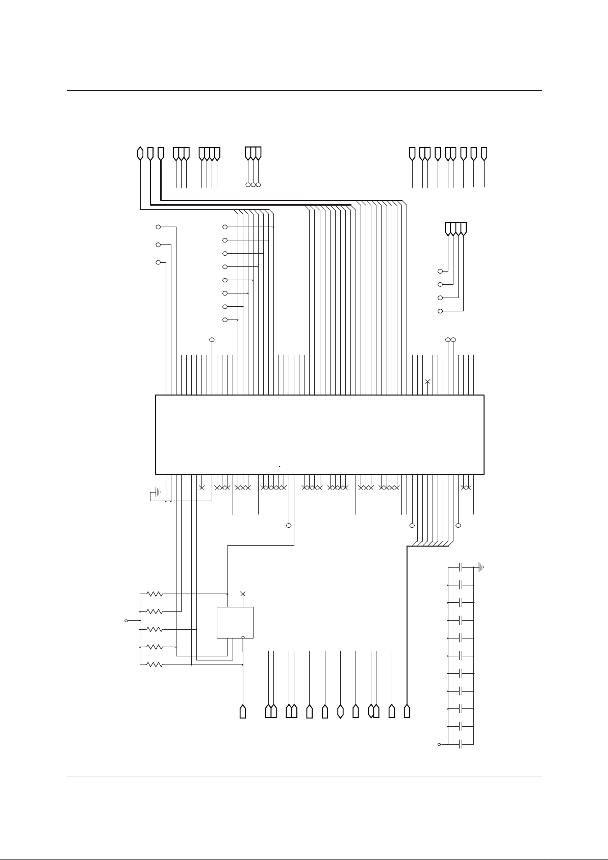
TMC22x5yA Digital Video Decoder
The TMC22x5yA accepts digitized video input on two
10-bit buses, “YOVER[9:0]” and “COVER[9:0]”. Based on
the status of its control registers, it then outputs the data to
the output edge connector of the board in a variety of
formats. Please see Table 1 for a listing of board default
video standards and output formats that are loadable to the
control registers.
After the TMC22x5yA control registers have been initially
loaded by the microcontroller, subsequent changes to the
control registers may be made through the R-bus interface
and Raydemo software.
It is important that the control registers be loaded correctly in
order to obtain the desired output. Once the control registers
have been set to output the correct data from the
TMC22x5yA, then several board switches must also be
correctly configured in order to obtain the desired output.
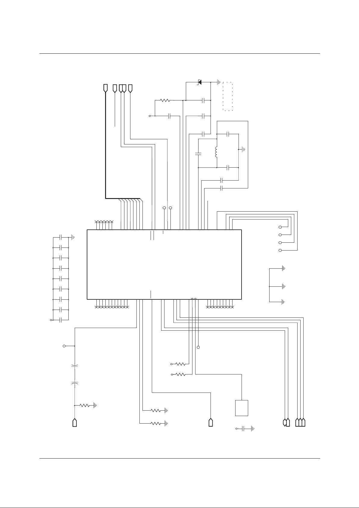
TMC2072 Genlocking Video Digitizer
The TMC2072 Genlocking Video Digitizer accepts analog
composite data through the composite input BNC on the left
side of the board. A 20MHz clock crystal provides the Genlock with an input clock. The TMC2072 outputs horizontal
and vertical syncs, and a 27MHz clock. The clock is used to
drive the Decoder and EPLD. Like the TMC22x5yA, the
Genlock part must be programmed at startup. Instructions on
how to do this are in the “Microcontroller” section of this
documentation.
EPLD
An Altera EPF10K10TC144-4 EPLD executes several
essential board functions. The EPLD serves as a buffer and
multiplexer for data buses and a register for several important control signals. These signals may be cross-referenced
to the included schematics. The EPLD control registers may
be modified using the Raydemo software. The Raydemo
EPLD R-bus address is 0000001. For a more complete
description or specification of signals going to or coming
from the TMC22x5yA and TMC2072, please refer to the
Fairchild Semiconductor Data Book (also available on CDROM) or the website at www.fairchildsemi.com.
Microcontroller
An Atmel 89C55 microcontroller is used to program the
TMC22x5yA and TMC2072 registers. The microcontroller
programs the parts through the R-bus at power up and reprograms them each time the “Reset” button is pushed. Please
see Table 1 on the next page for a description of available
microcontroller-programmed board configurations.
Table 1. TMB22153AMS100 Demonstration Board Video Standard Selection
P
3-0
Input Format Video Standard Output Format
0000 composite NTSC YUV
0001 Y/C NTSC YUV
0010 composite NTSC D1
0011 Y/C NTSC D1
0100 composite NTSC RGB
0101 composite, field-based NTSC YUV
0110 composite, field-based NTSC D1
0111 composite, frame-based NTSC YUV
1000 composite PAL YUV
1001 Y/C PAL YUV
1010 composite PAL D1
1011 Y/C PAL D1
1100 composite PAL RGB
1101 composite, field-based PAL YUV
1110 composite, field-based PAL D1
1111 reserved

PRELIMINARY INFORMATION TMB22153AMS100
3
Preliminary Information
Quick Setup/Verification for Composite NTSC
Input, YUV Output
1. Configure jumpers:
If using R-Bus interface, JP2 must be closed
(connected)
Leave JP1 open (unconnected)
Verify that JP4 is linked to the odd-numbered pins of
JP6
2. Configure slider-switches (push red slider TOWARD
specified marking on board) :
E1 “FPGA”
E2 “FPGA”
E3 “VS”
E4 “PXCK4\”
E5 “GP”
E6 “GH”
E7 “GV”
E8 “XP”
3. If you have reason to believe the bottom cover has been
removed, remove it and configure S4 as follows:
1-7 ON (low)
8 OFF (high)
4. Ensure BNC J1 (VIN1) is connected to composite
NTSC signal.
5. Ensure piano-key switches P
3-0
, Y are in the “LOW”
(down) position.
6. Plug in power-supply connector and apply power.
LED’s corresponding to applied voltages should lightup.
7. Press and release the MRST button (S2). The TMC2072
and TMC22x5yA should both be programmed. To
verify the TMC2072 is functioning correctly, check for
presence of a clock (TP sync pulses, VS (TP18) and
HS (TP17). Likewise, to verify the TMC22x5yA is
functioning, check for presence of DHSYNC (TP5) and
DVSYNC (TP6).
Power Supply Requirements
The TMB22153AMS100 power supply connector is on
the top edge of the board toward the left side. The
TMB22153AMS100 board requires DC power supply
voltages of +5V and -5V.
The +5V supply provides power and voltage references to
the TMC22x5yA and /TMC2072, as well as driving TTL
logic devices. It is for this reason that a bench power supply
with short cable lengths is recommended.

TMB22153AMS100 PRELIMINARY INFORMATION
4
Preliminary Information
POWER
POWER
SMA MODULES
SMA MODULES
YOVER[0..9]
COVER[0..9]
CLAMP
YOE10
AN COMP/LUMA
COE10
ADCLK1
ADCLK2
GENLOCK
GENLOCK
GRS T
GHSYNC
GVSYNC
GPXCK
CVBS[0..7]
VALID
AN COMP/LUMA
SDA
SCL
SA0
SA1
SA2
SIGNAL HEADER
OP-CONN
RV[0..9]
BU[0..9]
GY[0..9]
OHS
OVS
SDA
SCL
RESET
HREF
CREF
VALID
VREF
PGM_OUT
RGBD1NTSC/PAL
BLANK(DAC)
FID_0
Y[0..9]
MPU[0..4]
EDGE CONNECTOR
OP-CONN
RV[0..9]
BU[0..9]
OHS
OVS
SDA
SCL
RESET
DICECLK
HREF
CREF
VALID
VREF
PGM_OUT
RGBD1NTSC/PAL
BLANK(DAC)
FID_0
Y[0..9]
IXHSYNC
IXVSYN C
675MHZ
IXPXCK
135MHZ
FPGA
FPGA
SDA
SCL
MPU[0..7]
DCS B
DA1
DA0
CLAMP
CVBS[0..7]
DECCLK
SWW
COVER[0..9]
BLANK(DAC)
NTSC/PAL
D1
COE10
FSOE
RGB
HS
VS
PGM_OUT
FSER
BUFFER
MASTER0
MASTER1
YOE10
HREF
CREF
VREF
D1ENFS
PGM_START
DR W
OVS
OHS
AVOUT
DVS YNC
DHSYNC
675MHZ
YOVER[0..9]
FSET
CKDRIVE
CKDRIVE
DECCLK
DICECLK
ADCLK1
GVSYNC
GHSYNC
GPXCK
IXVSYN C
IXHSYNC
IXPXCK
ADCLK2
HS
VS
FSIN_CLK
DECODER
DECODER
HS
VS
YOVER[0..9]
COVER[0..9]
GY[0..9]
BU[0..9]
RV[0..9]
DHSYNC
DVS YNC
MPU[0..7]
DRST
DCS B
DA1
DA0
SCL
SDA
DECCLK
SWW
BUFFER
MASTER0
MASTER1
SA0
SA1
SA2
FID_0
DR W
AVOUT
FSET
FRAMESTORE CONNECTOR
FRAMESTORE CONNECTOR
YOVER[0..9]
COVER[0..9]
FSIN_CLK
HS
VS
FSER
SCL
SDA
RESET
FSOE
D1ENFS
IXPXCK
IXHSYNC
IXVSYN C
MCU
MCU
SDA
PGM_OUT
135MHZ
SCL
RESET
PGM_START
DRST
GRS T
GY[0..9]
BU[0..9]
RV[0..9]
SDA
RESET\
SCL
SWW
DHSYNC
DVS YNC
CREF
VALID
VREF
PGM_OUT
RGB
D1
COVER[0..9]
RESET\
SA0
SA1
SA2
NTSC/PAL
BLANK\(DAC)
HREF
YOE10
DRST\
COE10
CLAMP
YOVER[0..9]
YOVER[0..9]
ADCLK1
DICECLK
GVSYNC
IXPXCK
GHSYNC
IXHSYNC\
IXVSYNC\
GPXCK
ADCLK2
DECCLK
FSIN_CLK
ADCLK2
AVOUT
GRST\
GVSYNC
AN COMP/LUMA
GPXCK
SA2
SA1
SA0
GHSYNC
VALID
AN COMP/LUMA
OHS
D1
RGB
PGM_OUT
CREF
VALID
VREF
NTSC/PAL
HREF
FID_0
FID_0
DICECLK
SDA
RESET\
SCL
BLANK\(DAC)
OVS
OHS
GY[0..9]
BU[0..9]
RV[0..9]
OVS
Y[0..9]
Y[0..9]
FSIN_CLK
IXHSYNC\
IXVSYNC\
675MHZ
IXPXCK
CVBS[0..7]
COVER[0..9]
NTSC/PAL
BUFFER
MASTER1
DR W
AVOUT
HS
DA1
DA0
CLAMP
VREF
DCS B
D1
MASTER0
MPU[0..7]
DHSYNC
SDA
VS
HREF
SCL
SCL
DA0
COVER[0..9]
FSER FSER
SDA
SDA
DCS B
DECCLK
BLANK\(DAC)
FSOE FSOE
PGM_OUT
BUFFER
675MHZ
CREF
DVS YNC
SCL
RGB
SCL
MASTER0
SDA
MPU[0..7]
DA1
SWW
HS
MASTER1
OVS
OHS
D1ENFS
DR W
YOVER[0..9]
YOE10
COE10
VS
HS
VS
135MHZ
PGM_START
PGM_OUT
IXPXCK
IXHSYNC\
IXVSYNC\
135MHZ
RESET\
DRST\
GRST\
PGM_START
SDA
FSET
FSET
SCL
ADCLK1

PRELIMINARY INFORMATION TMB22153AMS100
5
Preliminary Information
C8 NOT INSTALLED
IF CR10 IS INSTALLED
VCC
VCC
VCC
VCC
VCC
GVSYNC
AGND
CVBS7
GPXCK
CVBS5
CVBS1
CVBS6
SA2
CVBS0
20MCLK
SDA
GVSYNC
CVBS3
GHSYNC
GND
GHSYNC
SCL
GPXCK
CVBS[0..7]
DGND
GRST\
CVBS2
CVBS4
SA0
SA1
VALID
SA1
SDA
GRST\
GPXCK
GHSYNC
SA0
AN COMP/LUMA
CVBS[0..7]
SA2
SCL
GVSYNC
TP5
TP
C13
6.8pF
C8
0.1uF
C4
0.1uF
R5
4.75K
R3
75
TP4
TP
+
C11
22uF/6.3v
C14
0.1uF
C19
150pF
C18
0.1uF
C20
390pF
U1
TMC2072KHC
VIN165VIN261VIN3
58
NC9NC
12
SA2
3
SCL
5
EXT PXCK
94
LDV
40
NC
85
NC19NC
20
CVBS021CVBS122CVBS528CVBS7
30
GHSYNC
32
GVSYNC
33
VALID
34
NC
13
FID0
35
VREF
70
COMP
88
RT68RB
57
NC
83
CBYP
75
PFD IN
77
NC10NC
14
CVBS4
25
FID2
37
NC
43
CLK IN
91
CVBS2
23
PXCK
45
CLK OUT
93
NC
99
SA01SA1
2
RESET
7
NC11NC
15
INT
17
CVBS324CVBS6
29
BURL
31
FID1
36
NC
47
NC53NC54NC56NC59NC62NC66NC71NC76NC
78
NC79NC
80
DDS OUT
82
NC
84
PXCK SEL
86
SDA
4
C7
0.1uF
TP2
TP
R6
4.75K
+
C10
22uF/6.3v
C9
0.1uF
R2
75
H3
1
TP3
TP
H1
1
C6
0.1uF
TP1
TP
R1
75
R4
3.3K
C21
0.1uF
C3
0.1uF
C16
0.1uF
Y1
20MHz
OUT
5
H2
1 C12
0.1uF
CR1
1.235V
2
1
L1
INDUCTOR
C1
0.1uF
C2
0.1uF
C15
0.1uF
C17
0.1uF
C5
0.1uF

TMB22153AMS100 PRELIMINARY INFORMATION
6
Preliminary Information
VCC
VCC
DECODER
PARALLEL
INTERFACE
SDA
CLAMP
YOE 10
SW W
AVOUT
SCL
PGM_OUT
COE10
FSOE
OVS
OHS
CREF
HREF
VREF
D1ENFS
DR W
DECCLK
HSVSDHSYNC
DVS YNC
FSER
CVBS5
CVBS3
CVBS2
CVBS7
CVBS4
CVBS1
CVBS[0..7]
CVBS6
OVS
BUFFER
DECCLK
D1
RGB
NTSC/PAL
BLANK\(DAC)
BUFFER
MASTER0
MASTER1
CLAMP
PGM_START
DA1
DCS B
DA0
SW W
COVER[0..9]
YOVER[0..9]
COE10
YOE 10
HS
VS
GRA B
LINE_GRAB
PIXEL_GRAB
CREF
MPU[0..7]
FSOE
FSER
D1ENFS
OHS
BLANK\(DAC)
SDA
HREF
VREFD1NTSC/PAL
PGM_OUT
RGB
SCL
DR W
COVER7
COVER0
COVER8
COVER9
COVER1
COVER6
COVER3
COVER2
COVER5
COVER4
YOVER2
YOVER3
YOVER8
YOVER1
YOVER6
YOVER9
YOVER5
YOVER4
YOVER0
YOVER7
AVOUT
PGM_START
DVS YNC
DHSYNC
MPU0
MPU3
MPU5
MPU6
MPU1
MPU2
MPU7
MPU4
MASTER0
MASTER1
CVBS0
FSET
FSET
C22
0.1uF
C23
0.1uF
C24
0.1uF
C25
0.1uF
C26
0.1uF
C27
0.1uF
C28
0.1uF
C30
0.1uF
H15
1
TP9
TP
TP8
TP
TP7
TP
TP6
TP
U9
EPC1PC8
DATA
1
DCLK
2
OE3nCS
4
nCASC
6
R39
1K
R38
1K
R37
1K
R36
1K
R40
1K
H9
1
H4
1H61H71
H11
1
TP30
TP
TP29
TP
TP31
TP
H12
1
U2
EPF10K10TC144
MSEL077MSEL176nSTATUS35nCONFIG74DCLK
107
CONF_DONE2INIT_DONE14nCE
106
nCEO3nWS
142
nRS
141
nCS
144CS143
RDYnB SY11CLKUSR7DATA7
116
DATA6
114
DATA0
108
DATA1
109
DATA2
110
DATA3
111
DATA4
112
DATA5
113
TDI
105
TDO4TCLK1TMS34DEDIN54DEDIN56DEDIN
124
DEDIN
126
GCLK0
125
GCLK155DEV_CLRn
122
DEV_OE
128
889910101212131318181919202021212222232326262727282829293030313132
32
333336363737383839394141424243434444464647474848494951515959606062626363646465656767686869697070727273737878797980808181828283838686878788888989909091919292959596969797989899
99
100
100
101
101
102
102
117
117
118
118
119
119
120
120
121
121
130
130
131
131
132
132
133
133
135
135
136
136
137
137
138
138
140
140
17
17
H101H5
1
TP25
TP
TP21
TP
TP27
TP
TP24
TP
TP26
TP
TP28
TP
TP22
TP
TP23
TP
C29
0.1uF
C64
0.1uF
C65
0.1uF
AVOUT
DHSYNC
DVS YNC
CVBS[0..7]
CLAMP
YOE 10
SW W
SDA
FSOE
OVS
OHS
COE10
SCL
D1ENFS
HREF
CREF
VREF
DR W
DECCLK
HS
VS
FSER
675MHZ
DCS B
DA1
DA0
NTSC/PAL
RGBD1BLANK\(DAC)
COVER[0..9]
BUFFER
MASTER0
MASTER1
YOVER[0..9]
PGM_START
MPU[0..7]
PGM_OUT
FSET
 Loading...