

Fairchild Semiconductor TIS98 Datasheet
TIS98
TIS98
Discrete POWER & Signal
Technologies
E
B
C
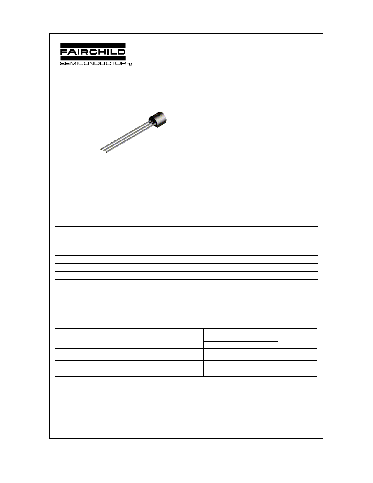
TO-92
NPN General Purpose Amplifier
This device is designed for use as general purpose amplifiers
and switches requiring collector currents to 300 mA. Sourced from
Process 10. See PN100 for characteristics.
Absolute Maximum Ratings* TA = 25°C unless otherwise noted
Symbol Parameter Value Units
V
CEO
V
CBO
V
EBO
I
C
TJ, T
stg
*These ratings are limiting values above which the serviceability of any semiconductor device may be impaired.
NOTES:
1) These ratings are based on a maximum junction temperature of 150 degrees C.
2) These are steady state limits. The factory should be consulted on applications involving pulsed or low duty cycle operations.
Thermal Characteristics TA = 25°C unless otherwise noted
Collector-Emitter Voltage 60 V
Collector-Base Voltage 80 V
Em i t ter - Bas e V olt ag e 6. 0 V
Collector Current - Continuous 500 mA
Operating and Storage Junction Temperature Range -55 to +150
°C
Symbol Characteri st ic Max Units
TIS98
P
D
R
θ
JC
R
θ
JA
1997 Fairchild Semiconductor Corporation
Total De vice Dissip at i on
Derate above 25°C
Thermal Resistance, Junction to Case 83.3 °C/W
Thermal Resistance, Junction to Ambient 200 °C/W
625
5.0
mW
mW/°C
NPN General Purpose Amplifier
(continued)
Electrical Characteristics TA = 25°C unless otherwise noted
Symbol Parameter Test Conditions Min Max Units
OFF CHARACTERISTICS
V
(BR)CEO
I
CBO
I
EBO
ON CHARACTERISTICS*
h
FE
V
sat
CE(
V
BE(on)
SMALL SIGNAL CHARACTERISTICS
C
cb
C
eb
h
fe
y
fe
C ollector - Emi tt er Breakdown Volt age* IC = 10 mA, IB = 0 60 V
Co lle c tor Cutoff Cu rre n t VCB = 40 V, IE = 0
= 80 V, IE = 0
V
CB
Emitter Cu toff Cu r re nt VEB = 6.0 V, IC = 0 20 nA
DC Cu r re n t Gai n VCE = 5.0 V, IC = 1.0 mA 100 300
Collector-Emitter Saturation Voltage IC = 10 mA, IB = 0.1 mA
)
= 100 mA, IB = 5.0 mA
I
C
Base-Emitter On Voltage IC = 1.0 mA, VCE = 5.0 V 0.5 0.7 V
Collector- Bas e Capacitanc e VCB = 5.0 V, f = 1.0 MHz 1.0 4.0 pF
Emitter-Base Capacitance VEB = 0.5 V, f = 1.0 MHz 16 pF
Small-Signal Current Gain IC = 1.0 mA, VCE = 5.0 V,
f = 1.0 kHz
= 10 mA, VCE = 5.0 V,
I
C
f = 100 MHz
Forwa r d Trans-co nductance IC = 1.0 mA, VCE = 5.0 V,
100
2.0
30 mmhos
f = 100 MHz
10
10
1.0
0.5
400
nA
µ
V
V
TIS98
A
*Pulse Test: Pulse Width ≤ 300 µs, Duty Cycle ≤ 2.0%
 Loading...