

Fairchild Semiconductor TIS74, TIS73 Datasheet
TIS73
TIS74
TIS73 / TIS74
G
S
D
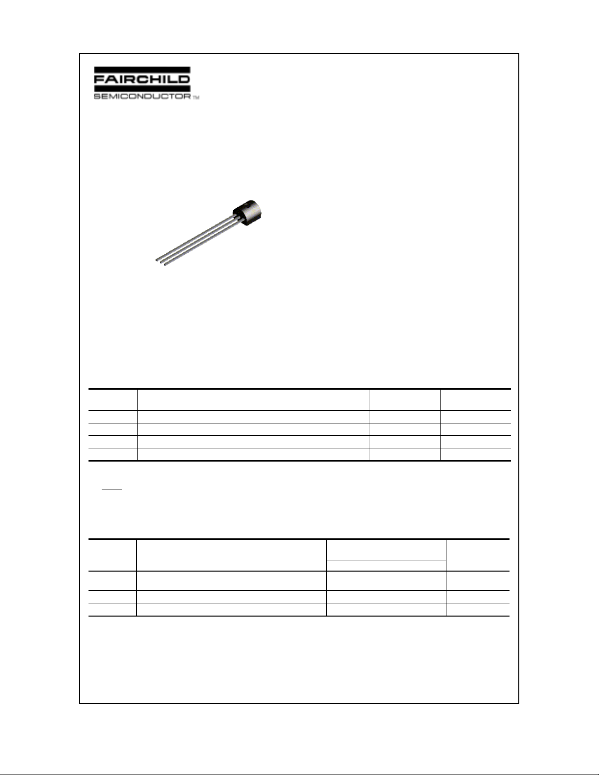
TO-92
N-Channel General Purpose Amplifier
This device is designed for low level analog switching, sample
and hold circuits and chopper stabalized amplifiers. Sourced from
Process 54.
Absolute Maximum Ratings* TA = 25°C unless otherwise noted
Symbol Parameter Value Units
V
DG
V
GS
I
GF
TJ, T
stg
*These ratings are limiting values above which the serviceability of any semiconductor device may be impaired.
NOTES:
1) These ratings are based on a maximum junction temperature of 150 degrees C.
2) These are steady state limits. The factory should be consulted on applications involving pulsed or low duty cycle operations.
Thermal Characteristics TA = 25°C unless otherwise noted
Drain-Gate Voltage 30 V
Ga t e- Sour c e V oltag e - 30 V
Forward Gate Current 10 mA
Operating and Storage Junction Temperature Range -55 to +150 °C
Symbol Characteri st ic Max Units
TIS73 / TIS74
P
D
R
θ
JC
R
θ
JA
1997 Fairchild Semiconductor Corporation
Total De vice Dissip at i on
Derate above 25°C
Thermal Resistance, Junction to Case 83.3
Thermal Resistance, Junction to Ambient 200 °C/W
625
5.0
mW
mW/°C
°C/W
N-Channel General Purpose Amplifier
(continued)
Electrical Characteristics TA = 25°C unless otherwise noted
Symbol Parameter Test Conditions Min Max Units
OFF CHARACTERISTICS
- 30 V
- 2.0
- 5.0
- 2.0
- 5.0
- 4.0
- 2.0
- 10
- 6.0
20 100
25
40
nA
µ
nA
µ
V
V
mA
mA
Ω
Ω
I
V
GSS
I
V
D(
(BR)GSS
off
)
off
GS(
Gate-Source Breakdown Voltage
Gate Reverse Current VGS = 15 V, VDS = 0
D r ain Cutof f Leakage C urrent VDS = 15 V, VGS = 10 V
Gate-Source Cutoff Voltage VDS = 15 V, ID = 4.0 nA TIS73
)
ON CHARACTERISTICS
I
DSS
r
DS(on)
Zero-Gate Voltage Drain Current* VDS = 15 V, VGS = 0 50
Drain- So ur ce On Resistance
SMALL-SIGNAL CHARACTERISTICS
C
iss
Input Capacitance VDS = 0, VGS = 10 V, f = 1.0 MHz 18 pF
= 1.0 µA, VDS = 0
I
G
= 15 V, VDS = 0, TA = 100°C
V
GS
= 15 V, VGS = 10 V, TA = 100°C
V
DS
TIS74
≤ 0.1 V, VGS = 0, TIS73
V
DS
f = 1.0 kHz TIS74
TIS73 / TIS74
A
A
C
rss
Reverse Transfer Capacitance VDS = 0, VGS = 10 V, f = 1.0 MHz 8.0 pF
SWITCHING CHARACTERISTICS
t
r
t
on
t
off
Rise Time
Turn-On Time
Turn-Off Time
*Pulse Test: Pulse Width ≤ 300 µs, Duty Cycle ≤ 3.0%
V
GS(
off)
= 20 mA, V
I
D
V
off)
GS(
= 20 mA, V
I
D
V
off)
GS(
= 20 mA, V
I
D
= 10 mA ,V
DS
= 10 mA ,V
DS
= 10 mA ,V
DS
= 0,
GS(
on)
= 10 V TIS73
TIS74
= 0,
on)
GS(
= 10 V
= 0,
on)
GS(
= 10 V TIS73
TIS74
3.0
4.0
ns
ns
6.0 ns
25
50
ns
ns
 Loading...