

Fairchild Semiconductor SSD2009A Datasheet
Dual N-CHANNEL POWER MOSFET
SSD2009A
FEATURES
! Lower R
! Improved Inductive Ruggedness
! Fast Switching Times
! Low Input Capacitance
! Extended Safe Operating Area
! Improved High Temperature Reliability
DS(ON)
Product Summary
DSS
R
DS(on)
Ω
Part Number
BV
SSD2009 50V 0.13
Absolute Maximum Ratings
Characteristic UnitsSymbol
V
DSS
I
D
I
DM
V
GS
P
D
T
, T
J
STG
Drain-to-Source Voltage
Continuous Drain Current T
Continuous Drain Current T
Drain Current-Pulsed ①
Gate-to-Source Voltage
Total Power Dissipation ( T
Operating and Junction Storage
Temperature Range
3.0A
( T
I
D
=25℃
A
=70℃
A
=25℃ )
A
=70℃ )
A
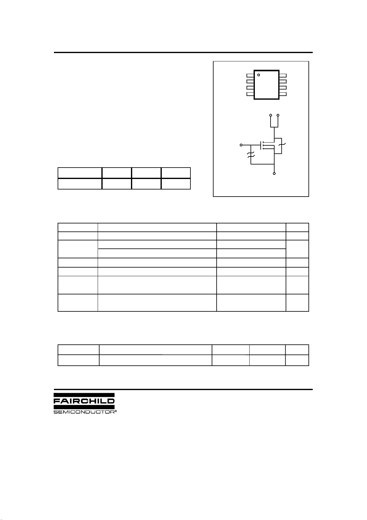
8 SOIC
G1 ,G
1
S
1
2
G
1
3
S
2
4
G
2
Top View
D1,D
2
2
N -Channel MOSFET
▼
▼
▼
Value
50
3.0
2.3
10.0
±20
2.0
1.3
- 55 to +150
S1 ,S
2
8
7
6
5
D1,D
D
1
D
1
D
2
D
2
2
▼
V
A
A
V
W
℃
Thermal Resistance
R
θJA
Characteristic Max. UnitsSymbol Typ.
Junction-to-Ambient
-- 62.5
℃/W
Rev. A1
SSD2009A
Dual N-CHANNEL
POWER MOSFET
Electrical Characteristics
CharacteristicSymbol
BV
V
I
I
I
R
t
t
GS(th)
GSS
DSS
DON
DS(on)
g
d(on)
d(off)
Q
Q
Q
Drain-Source Breakdown Voltage
DSS
Gate Threshold Voltage
Gate-Source Leakage , Forward
Gate-Source Leakage , Reverse
Drain-to-Source Leakage Current
On-State Drain-Source Current
Static Drain-Source
On-State Resistance ②
Forward Transconductance ②
fs
Turn-On Delay Time
t
Rise Time
r
Turn-Off Delay Time
t
Fall Time
f
Total Gate Charge
g
Gate-Source Charge
gs
Gate-Drain (“Miller”) Charge
gd
(TC=25℃ unless otherwise specified)
Max. UnitsTyp.Min. Test Condition
V
50
1.0
--
--
--
--
10
--
--
--
--
--
--
--
--
--
--
--
--
--
--
--
--
--
0.065
0.084
7.0
16
16
40
23
17
1.8
3.9
--
3.0
100
-100
2.0
25
--
0.13
0.2
--
20
20
70
50
25
--
--
V
V
nA
nA
μA
AV
Ω
S
ns
nC
=0V,ID=250μA
GS
V
= 5V ,ID=250μA
DS
V
=20V
GS
V
=-20V
GS
V
=40V
DS
VDS=40V,TC=55℃
=5V ,VGS=10V
DS
V
=10V,ID=3.0A
GS
V
=4.5V,ID=1.5A
GS
VDS=15V,ID=3.0A
VDD=25V,ID=1.0A,
R
=6.0Ω,
0
V
=25V,VGS=10V,
DS
ID=2.0A ②③
②③
Source-Drain Diode Ratings and Characteristics
CharacteristicSymbol Max. UnitsTyp.Min. Test Condition
Continuous Source Current
I
S
(Body Diode)
V
Diode Forward Voltage ②
SD
Reverse Recovery Time ②
t
rr
Notes ;
① Repetitive Rating : Pulse Wi dth Lim i ted by Maximum Junction Temperature
② Pulse Test : Pulse Width = 250μs, Duty Cycl e ≤ 2%
③ Essentially Independent of Operating Temperature
--
--
100
2.0
1.2
--
--
--
--
Modified MOSFET Symbol
Showing the Integral Reverse
A
P-N Junction Rectifier
V
TA=25℃,IS=1.5A,VGS=0V
ns
T
=25℃,IF=1.5A,diF/dt=100A/μs
A
D
○
││││
││││
────
────
▲
││││
◀
││││
────
││││
││││
││││
○
────
┘┘┘┘
────
G
││││
S
○
 Loading...