

Fairchild Semiconductor SFF9250L Datasheet

Advanced Power MOSFET
SFF9250L
FEATURES
❑ Logic-Level Gate Drive
❑ Avalanche Rugged Technology
❑ Rugged Gate Oxide Technology
❑ Lower Input Capacitances
❑ Improved Gate Charge
❑ Extended Safe Operating Area
❑ Lower Leakage Current : 10uA (Max.) @ VDS=-200V
❑ Lower R
: 0.175 Ω (Typ.)
DS(ON)
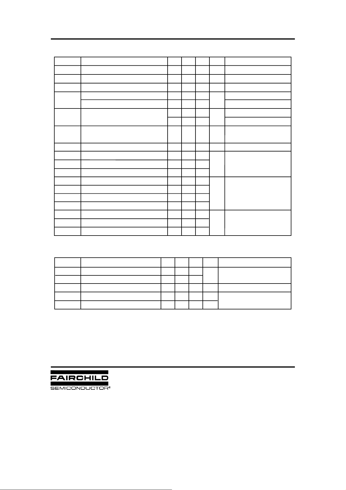
Absolute Maximum Ratings
Characteristic Value UnitsSymbol
Drain-to-Source Voltage
Continuous Drain Current (T
Continuous Drain Current (T
=25 °C)
C
=100 °C)
C
Drain Current-Pulsed
Gate-to-Source Voltage
Single Pulsed Avalanche Energy #
Avalanche Current
Repetitive Avalanche Energy
Peak Diode Recovery dv/dt
Total Power Dissipation (TC=25 °C)
Linear Derating Factor
Operating Junction and
Storage Temperature Range
Maximum Lead Temp. for Soldering
Purposes, 1/8% from case for 5-seconds
T
V
DSS
I
I
DM
V
E
I
AR
E
dv/dt
P
, T
J
T
D
GS
AS
AR
D
STG
L
"
"
"
$
BV
DSS
R
DS(on)
ID= -12.6 A
TO-3PF
1
2
3
1.Gate 2. Drain 3. Source
-200
-12.6
-7.9
-50.4
!20
990
-12.6
20.4
-5.0
90
0.72
- 55 to +150
300
= -200 V
= 0.23 Ω
V
A
A
V
mJ
A
mJ
V/ns
W
W/ °C
°C
Thermal Resistance
R
&JC
R
&JA
Characteristic Max. UnitsSymbol Typ.
Junction-to-Case
Junction-to-Ambient
--
--
0.61
40
°C/W
Rev. A
SFF9250L
P-CHANNEL
POWER MOSFET
Electrical Characteristics
CharacteristicSymbol
BV
BV/,T
,
V
R
GS(th)
I
GSS
I
DSS
DS(on)
g
C
C
C
t
d(on)
t
d(off)
Q
Q
Q
Drain-Source Breakdown Voltage
DSS
Breakdown Voltage Temp. Coeff.
J
Gate Threshold Voltage
Gate-Source Leakage , Forward
Gate-Source Leakage , Reverse
Drain-to-Source Leakage Current
Static Drain-Source
On-State Resistance
Forward Transconductance
fs
Input Capacitance
iss
Output Capacitance
oss
Reverse Transfer Capacitance
rss
Turn-On Delay Time
t
Rise Time
r
Turn-Off Delay Time
t
Fall Time
f
Total Gate Charge
g
Gate-Source Charge
gs
Gate-Drain(Miller) Charge
gd
(TC=25°C unless otherwise specified)
Max. UnitsTyp.Min.
V
-200
--
-1.0
--
--
--
--
--
--
--
--
--
--
--
--
--
--
--
--
--
-0.17
--
--
--
--
--
.175
13
2500
400
210
20
150
100
65
90
12
54
--
--
-2.0
100
-100
10
100
0.23
--
3250
520
270
50
310
210
140
120
--
--
V
V/ °C
V
nA
)A
Ω
S
pF
ns
nC
=0V,ID=-250)A
GS
I
=-250)A See Fig 7
D
V
=-5V,ID=-250)A
DS
V
=-20V
GS
VGS=20V
V
=-200V
DS
V
=-160V,TC=125 °C
DS
V
=-5V,ID=-6.3A
GS
VDS=-40V,ID=-6.3A
=0V,VDS=-25V,f =1MHz
V
GS
VDD=-100V,ID=-12.6A,
R
=6.2Ω
G
VDS=-160V,VGS=-5V,
ID=-12.6A
See Fig 6 & Fig 12
Test Condition
See Fig 5
See Fig 13
*
*
*+
*+
Source-Drain Diode Ratings and Characteristics
CharacteristicSymbol Max. UnitsTyp.Min. Test Condition
--
--
--
260
2.8
-12.6
-50.4
-1.5
--
--
I
I
SM
V
t
Q
Notes ;
" Repetitive Rating : Pulse Wi dth Lim i ted by Maximum Junction Temperature
# L=3.9mH, I
$ I
* Pulse Test : Pulse Width ( 300)s, Duty Cycle ( 2%
+ Essentially Independent of Operating Temperature
Continuous Source Current
S
Pulsed-Source Current "
Diode Forward Voltage
SD
Reverse Recovery Time
rr
Reverse Recovery Charge
rr
=-19.5A, VDD=-50V, RG=27Ω, Starting TJ =25'
AS
(-19.5A, di/dt(500A/)s, VDD(BV
SD
--
--
*
--
--
--
, Starting TJ =25'
DSS
Integral reverse pn-diode
A
in the MOSFET
V
T
ns
T
)C
di
=25 °C,IS=-12.6A,VGS=0V
J
=25 °C,IF=-19.5A,VDD=-160V
J
/dt=100A/)s
F
*
P-CHANNEL
POWER MOSFET
SFF9250L
-
Note :
1. 250.s Pulse Te st
'
= 25
2. T
C
0
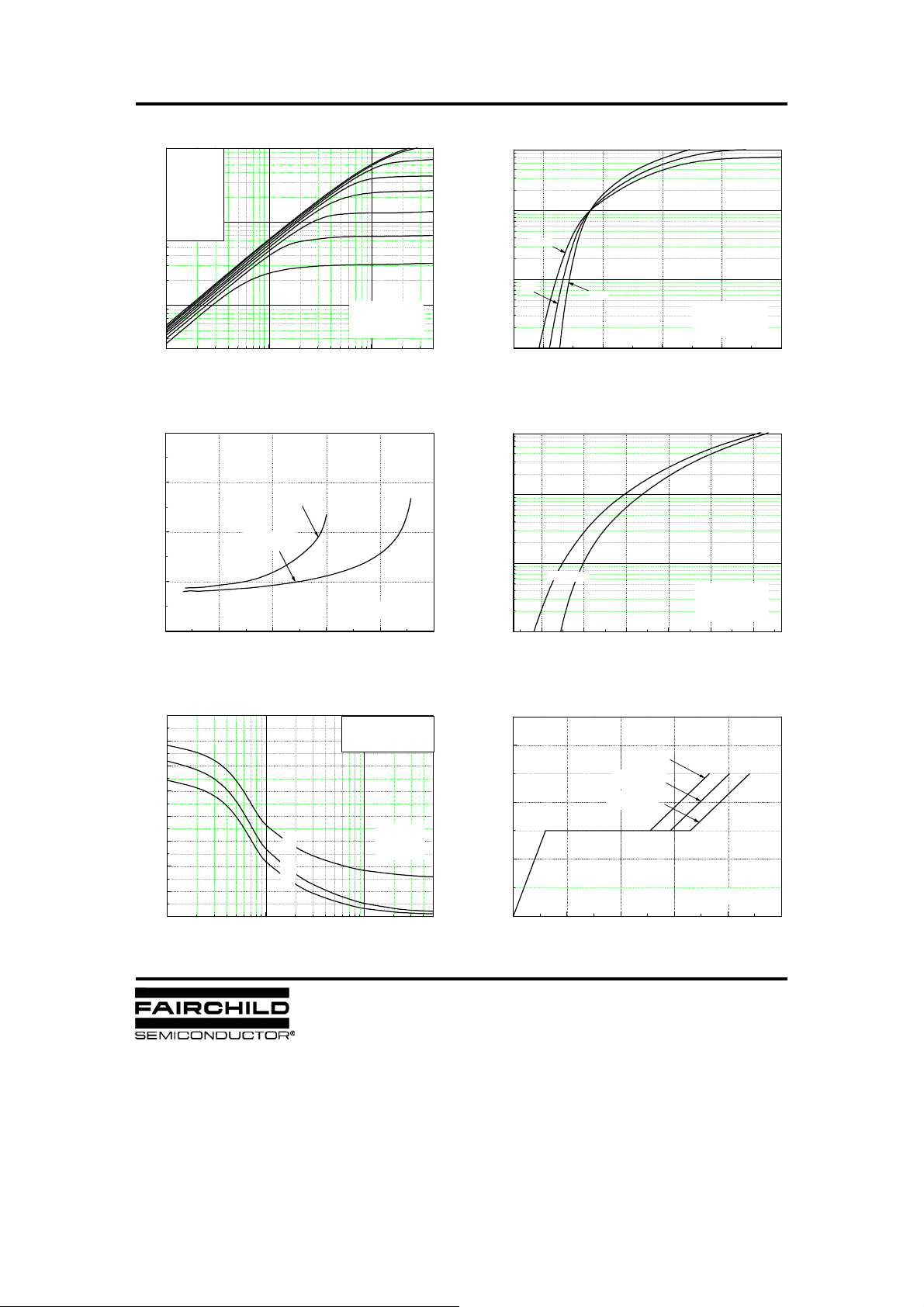
10
1
10
10
, Drain Current [A]
D
-I
10
V
Top : -10.0 V
-8.0 V
-6.0 V
-5.0 V
-4.5 V
-4.0 V
1
-3.5 V
Bottom : -3.0 V
0
-1
10
Fig 1. Output Characteristics Fig 2. Transfer Characteristics
GS
-VDS, Drain-Source Voltage [V]
0.8
0.6
VGS = - 10V
VGS = - 5V
-
Note : T
J
= 25
'
]
Ω
, [
0.4
DS(on)
R
0.2
Drain-Source On-Resistance
0.0
0 20406080100
-ID , Drain Current [A]
1
10
'
150
0
10
'
25
, Drain Current [A]
D
-I
-1
10
246810
'
-55
-
Note
= -40V
1. V
DS
2. 250.s Pulse Test
-VGS , Gate-Source Voltage [V]
Fig 4. Source-Drain Diode Forward VoltageFig 3. On-Resistance vs. Drain Current
1
10
0
10
, Reverse Drain Current [A]
DR
-I
-1
10
'
150
'
25
-
Note :
= 0V
1. V
GS
2. 250.s Pulse Test
0.6 1.2 1.8 2.4 3.0 3.6
-VSD , Source -Drain V o lta g e [V]
Capacitances [pF]
12000
10500
9000
7500
6000
4500
3000
1500
C
= Cgs + Cgd (Cds = shorted)
iss
= Cds + C
C
oss
gd
C
= C
rss
gd
Fig 6. Gate Charge vs. Gate-Source VoltageFig 5. Capacitance vs. Drain-Source Voltage
6
VDS = -40V
VDS = -100V
4
-
10
1
Note ;
1. V
= 0 V
GS
2. f = 1 MHz
C
iss
C
oss
C
rss
0
-1
10
0
10
2
, Gate-Source Voltage [V]
GS
-V
0
020406080100
-VDS, Drain-Source Voltage [V]
VDS = -160V
QG, Total Gate Cha rge [nC]
-
Note : I
= -19.5 A
D
 Loading...