

Fairchild Semiconductor SCAN182374ASSC, SCAN182374ASSCX Datasheet
© 2000 Fairchild Semiconductor Corporation DS011545 www.fairchildsemi.com
January 1993
Revised August 2000
SCAN182374A D-Type Flip-Flop with 25
Ω
Series Resistor Outputs
SCAN182374A
D-Type Flip-Flop with 25
Ω Series Resistor Outputs
General Description
The SCAN182374A is a high performance BiCMOS D-type
flip-flop featuring separate D-type inputs organized into
dual 9-bit bytes with byte -orien ted clock a nd out put ena ble
control signals. This device is compliant with IEEE 1149.1
Standard Test Access Port and Boundary Scan Architecture with the incorporat ion of the defined boundary-scan
test logic and test access port consisting of Test Data Input
(TDI), Test Data Out (TDO), Test Mode Select (TMS), and
Test Clock (TCK).
Features
■ IEEE 1149.1 (JTAG) Compliant
■ High performance BiCMOS technology
■ 25
Ω series resistor outputs elim inate need for external
terminating resistors
■ Buffered positive edge-triggered clock
■ 3-STATE outputs for bus-oriented applications
■ 25 mil pitch SSOP (Shrink Small Outline Package)
■ Includes CLAMP, IDCODE and HIGHZ instructions
■ Additional instructions SAMPLE -IN, SAM P LE-O U T and
EXTEST-OUT
■ Power up 3-STATE for hot insert
■ Member of Fairchild’s SCAN Products
Ordering Code:
Device also available in Tape and Reel. Specify by appending the suffix letter “X” to the ordering code.
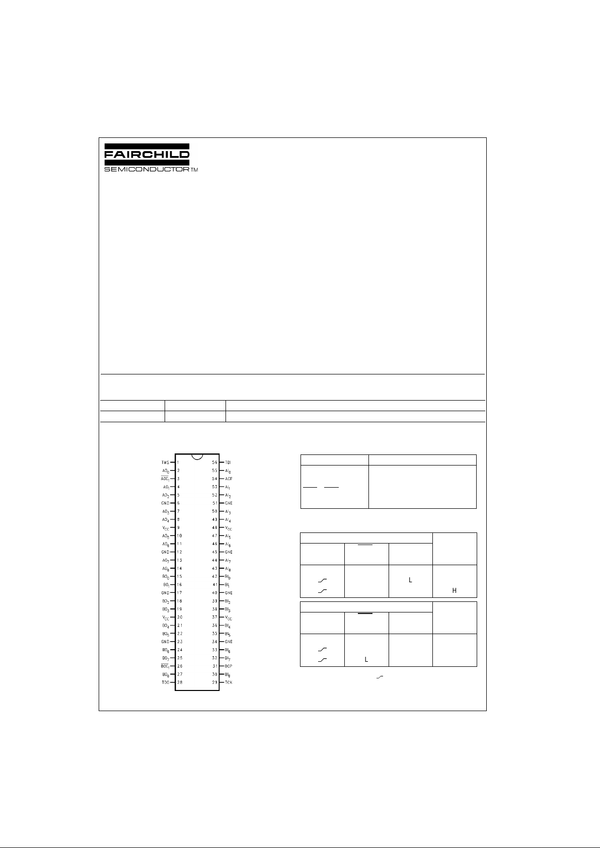
Connection Diagram Pin Descriptions
Tru th Tables
H = HIGH Voltage Level Z = High Impedance
L = LOW Voltage Level
= L-to-H Transition
X = Immaterial
Note 1: Inactive-to-active transition must occur to enable outputs upon
power-up.
Order Number Package Number Package Description
SCAN182374ASSC MS56A 56-Lead Shrink Small Outline Package (SSOP), JEDEC MO-118, 0.300 Wide
Pin Names Description
AI
(0–8)
, BI
(0–8)
Data Inputs
ACP, BCP Clock Pulse Inputs
AOE
1
, BOE
1
3-STATE Output Enable Inputs
AO
(0–8)
, BO
(0–8)
3-STATE Outputs
Inputs
AO
(0–8)
ACP AOE1
(Note 1)
AI
(0–8)
XHXZ
LLL
LHH
Inputs
BO
(0–8)
BCP BOE
1
(Note 1)
BI
(0–8)
XHXZ
LLL
LHH

www.fairchildsemi.com 2
SCAN182374A
Functional Description
The SCAN182374A consi sts of two sets of nine edge- triggered flip-flops with individual D-type inputs and 3-STATE
true outputs. The buffered clock and buffered Output
Enable pins are co mmon to all flip-flops. Each set of the
nine flip-flops will store the state of their individual D inputs
that meet the setup and hold time requirements on the
LOW-to-HIGH Clock (ACP or BCP) transition. With the
Output Enable (AOE
1
or BOE1) LOW, the contents of the
nine flip-flops are available at the outputs. When the Output
Enable is HIGH, the outputs go to the high impedance
state. Operation of the Output Enable inp ut does not affect
the state of the flip-flops.
Logic Diagram
Please note that this diagram is provided only for the understanding of logic operations and should not be used to estimate propagation delays.
Block Diagrams
Byte-A
Note: BSR stands for Boun dary Scan Register
Tap Controller

3 www.fairchildsemi.com
SCAN182374A
Block Diagrams (Continued)
Byte-B
Note: BSR stands for BOUNDARY-SCAN Register
Description of BOUNDARY-SCAN Circuitry
The scan cells used in the BOUNDARY-SCAN register are
one of the followin g two types de pending upon t heir location. Scan cell TYPE1 is intended to solely observe system
data, while TYPE2 has the additional ability to control system data.
Scan cell TYPE1 is located on each system input pin while
scan cell TYPE2 is locate d at each system output pin as
well as at each of the two internal active-high output enable
signals. AOE controls the activity of the A-outputs while
BOE controls the activity of the B-outputs. Each will activate their respective outputs by loading a logi c high.
The BYPASS register is a single bit shift register stage
identical to scan cell TYPE1. It captures a fixed logic low.
Bypass Register Scan Chain Definition
Logic 0
SCAN182374A Product IDCODE
(32-Bit Code per IEEE 1149.1)
The INSTRUCTION r egist er is a n 8-b it r egister whic h captures the default valu e of 10000 001 (SAM PLE/PRE LOAD)
during the CAPTURE-IR inst ructi on comm and. Th e benef it
of capturing SAMPLE/PRELOAD as the default instruction
during CAPTURE-IR is that the user is no longer required
to shift in the 8-bit instruction for SAMPLE/P RELOAD . The
sequence of: CAPTURE-IR
→ EXIT1-IR → UPDATE-IR
will update the SAMPLE/PRELOAD instruction. For more
information refer to the section on instruction definitions.
Instruction Register Scan Chain Definition
Version Entity Per Manufacturer Required
Number ID by 1149.1
0000 111111 0000000111 00000001111 1
MSB LSB
MSB → LSB
Instruction Code Instruction
00000000 EXTEST
10000001 SAMPLE/PRELOAD
10000010 CLAMP
00000011 HIGH-Z
01000001 SAMPLE-IN
01000010 SAMPLE-OUT
00100010 EXTEST-OUT
10101010 IDCODE
11111111 BYPASS
All Other BYPASS

www.fairchildsemi.com 4
SCAN182374A
Description of BOUNDARY-SCAN Circuitry (Continued)
Scan Cell TYPE1
Scan Cell TYPE2
 Loading...