

Fairchild Semiconductor SCAN182373ASSC, SCAN182373ASSCX Datasheet
SCAN182373A
SCAN182373A Transparent Latch with 25
January 1993
Revised August 2000
Transparent Latch with 25
General Description
The SCAN182373A i s a high performa nce BiCMOS transparent latch featur ing separate dat a inputs organized in to
dual 9-bit bytes wit h byte-or iented latch enable and output
enable control signals. This devi ce is compliant with IEEE
1149.1 Standard Test Access Port and Boundary-Scan
Architecture with the incorporation of the defined boundaryscan test logic and test access por t con sistin g of Test Data
Input (TDI), Test Data Out (TDO), Test Mode Select (TMS),
and Test Clock (TCK).
Ω Series Resistor Outp u t s
Features
■ IEEE 1149.1 (JTAG) Compliant
■ High performance BiCMOS technology
■ 25
Ω series resistor outputs elim inate need for external
terminating resistors
■ Buffered active-low latch enable
■ 3-STATE outputs for bus-oriented applications
■ 25 mil pitch SSOP (Shrink Small Outline Package)
■ Includes CLAMP, IDCODE and HIGHZ instructions
■ Additional instructions SAMPLE-IN, SAMPLE-OUT and
EXTEST-OUT
■ Power up 3-STATE for hot insert
■ Member of Fairchild’s SCAN Products
Ordering Code:
Order Number
SCAN182373ASSC MS56A 56-Lead Shrink Small Outline Package (SSOP), JEDEC MO-118, 0.300 Wide
Devices also availab l e in Tape and Reel. Specify by appending th e s uffix let t er “X” to the ordering code.
Package
Number
Package Description
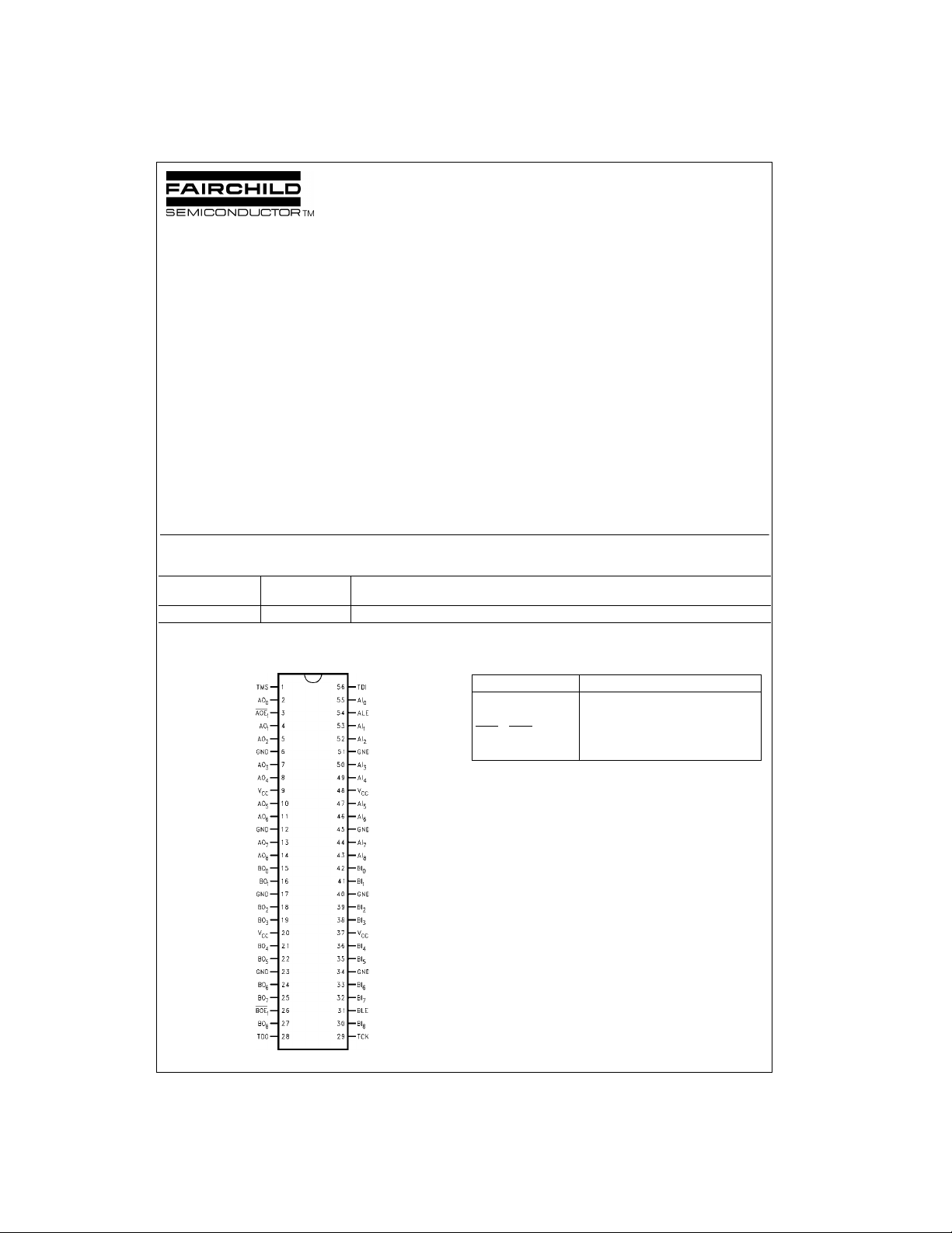
Connection Diagram Pin Descriptions
Pin Names Description
AI
, BI
(0–8)
1
(0–8)
, BOE
, BO
(0–8)
1
(0–8)
ALE, BLE Latch Enable Inputs
AOE
AO
Data Inputs
3-STATE Output Enable Inputs
3-STATE Latch Outputs
Ω
Series Resistor Outputs
© 2000 Fairchild Semiconductor Corporation DS011544 www.fairchildsemi.com
Truth Tables
Inputs
ALE
†AOE
AI (0–8)
1
XHXZ
HLLL
SCAN182373A
HLHH
LLXAO
H = HIGH Voltage Level
L = LOW Voltage Level
X = Immaterial
Z = High Impedance
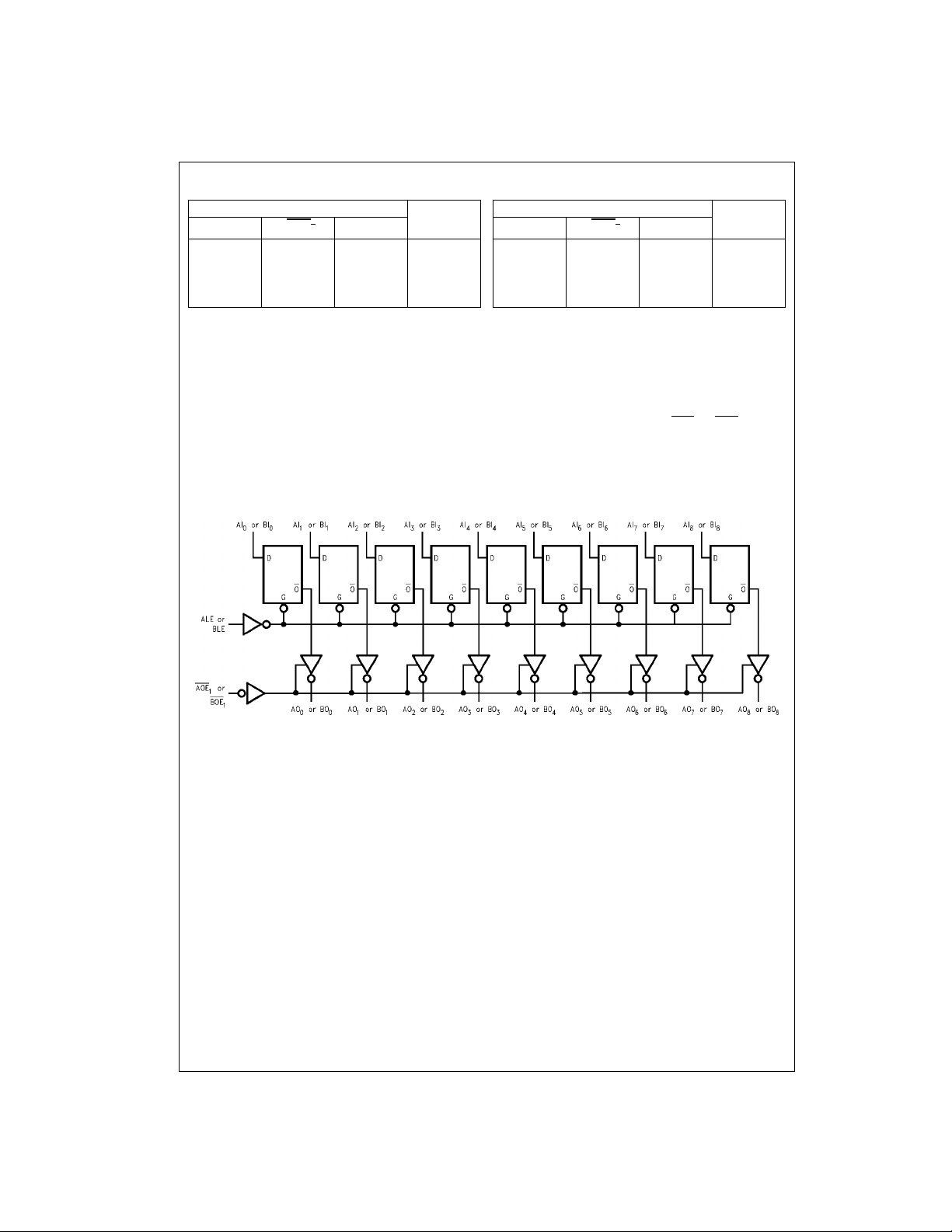
Functional Description
The SCAN182373A consists of two sets of nine D-type
latches with 3-STATE standard outputs. When the Latch
Enable (ALE or BLE) input is HIGH, data on the inputs
(AI
(0–8)
or BI
) enters the latches. In this condition the
(0–8)
latches are transparent, i.e., a latch output will change
state each time its inp ut changes. When Latch Enable is
LOW, the latches store the information that was presen t on
Logic Diagram
AO (0–8)
0
BLE
Inputs
†BOE
BI (0–8)
1
BO (0–8)
XHXZ
HLLL
HLHH
LLXBO
AO0 = Previous AO before H-to-L transition of ALE
BO
= Previous BO before H-to-L transition of BLE
0
† = Inactive-to-ac ti ve tr ans ition must occur to enable outputs upon
power-up.
0
the inputs a set-up t ime prec eding the HIGH-to- LOW transition of the Latch E nable. The 3 -STATE standard outputs
are controlled by the Outpu t En able (A OE
or BOE1) input.
1
When Output Enabl e is LOW, the standard outp uts are in
the 2-state mode. When Output E nable is HIGH, the standard outputs are in the high impedance mode, but this
does not interfere with entering new data into the latches.
Please note that this diagram is provided only for the understanding of logic operations and should not be used to estimate propagation delays.
www.fairchildsemi.com 2
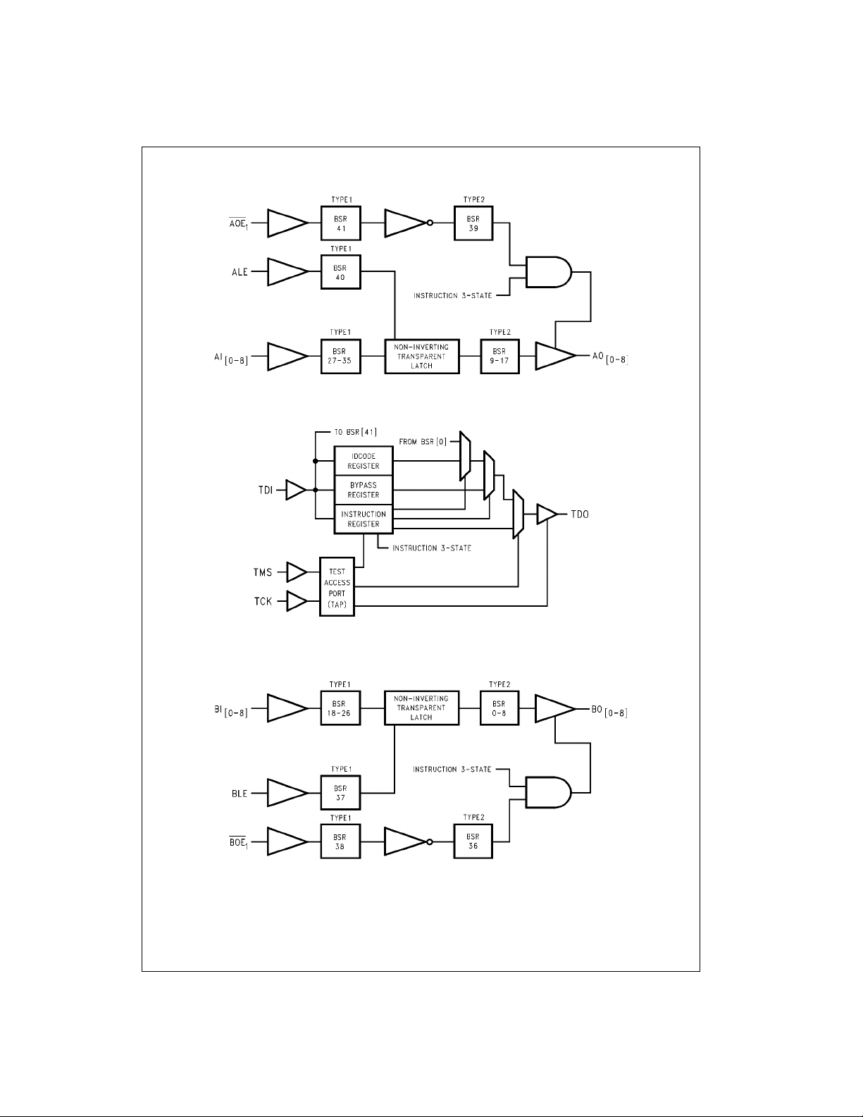
Block Diagrams
SCAN182373A
Byte-A
Tap Controller
Note: BSR stands for Boundary Sc an Register.
Byte-B
3 www.fairchildsemi.com
Description of BOUNDARY-SCAN Circuitry
The scan cells used in the BOUNDARY- SCAN register are
one of the foll owing two types depending upon their location. Scan cell TYPE1 is intended to solely observe system
data, while TYPE2 has the additional ability to control system data.
Scan cell TYPE 1 is located on each system input pin while
SCAN182373A
scan cell TYPE2 is located at each system output pin as
well as at each of the two internal active-high output enable
signals. AOE controls the activity of the A-outputs while
BOE controls the activity of the B-outputs. Each will activate their respective outputs by loading a logic high.
The BYPASS register is a single bit shift register stage
identical to scan cell TYPE1. It captures a fixed logic low.
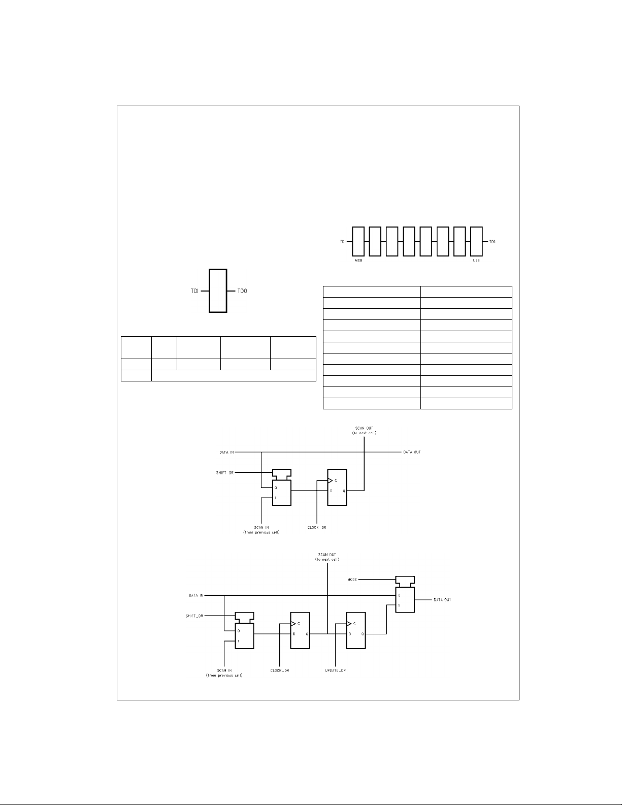
Bypass Register Scan Chain Definition
SCAN182373A Product IDCODE
(32-Bit Code per IEEE 1149.1)
Version Entity Part Manufacturer Required by
0000 111111 0000001000 00000001111 1
MSB LSB
Logic 0
Number ID 1149.1
The INSTRUCTION register is an 8-bit register which captures the default val ue of 10 000001 (SA MPLE/PR ELOAD)
during the CAPTURE-IR instr uctio n command . The ben efit
of capturing SAMPL E/PRELOAD a s the defau lt instru ction
during CAPTURE-IR is that the user is n o longer re quired
to shift in the 8-bit instruction fo r SAMP LE/PRELOA D. The
sequence of: CAPTURE-IR
will update the SAMPLE/PRELOAD instruction. For more
information refer to the section on instruction definitions.
Instruction Register Scan Chain Definition
MSB → LSB
Instruction Code Instruction
00000000 EXTEST
10000001 SAMPLE/PRELOAD
10000010 CLAMP
00000011 HIGH-Z
01000001 SAMPLE-IN
01000010 SAMPLE-OUT
00100010 EXTEST-OUT
10101010 IDCODE
11111111 BYPASS
All Others BYPASS
→ EXIT1-IR → UPDATE-IR
Scan Cell TYPE1
Scan Cell TYPE2
www.fairchildsemi.com 4
 Loading...