

Fairchild Semiconductor SCAN182245ASSC, SCAN182245ASSCX Datasheet

SCAN182245A
Non-Inverting Transceiver
with 25
Ω Series Resistor Outputs
SCAN182245A Non-Inverting Transceiver with 25
December 1993
Revised August 2000
General Description
The SCAN182245 A is a high perf ormance BiCMOS b idirectional line driver featuring separate data inputs organized into dual 9-b it b y te s wit h b yte -or iented output ena ble
and direction control signals. This device is compliant with
IEEE 1149.1 Standard Test Access Port and Boundary
Scan Architecture with the incorporation of the defined
boundary-scan test logi c an d t est acce ss po rt cons i sting of
Test Data Input (TDI), Test Data Out (TDO), Test Mode
Select (TMS), and Test Clock (TCK).
Features
■ High performance BiCMOS technology
Ω series resistors in outputs eliminate the need for
■ 25
external terminating resistors
■ Dual output enable control signals
■ 3-STATE outputs for bus-oriented applications
■ 25 mil pitch SSOP (Shrink Small Outline Package)
■ IEEE 1149.1 (JTAG) Compliant
■ Includes CLAMP, IDCODE and HIGHZ instructions
■ Additional instructions SAMPL E-IN, SAM P LE -O UT and
EXTEST-OUT
■ Power Up 3-STATE for hot insert
■ Member of Fairchild’s SCAN Products
Ordering Code:
Order Number Package Number Package Description
SCAN182245ASSC MS56A 56-Lead Shrink Small Outline Package (SSOP), JEDEC MO-118, 0.300 Wide
Devices also availab l e in Tape and Reel. Specify by appending th e s uffix let t er “X” to the ordering code.
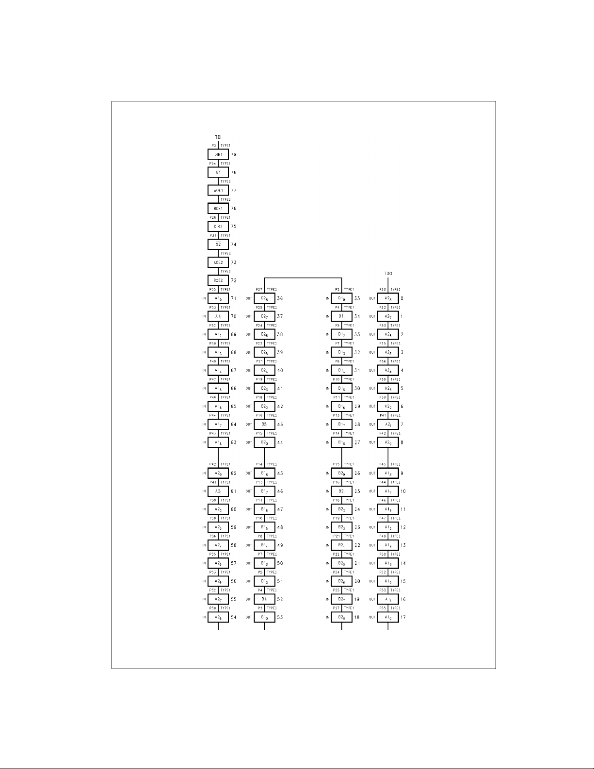
Connection Diagram Pin Descriptions
Pin Names Description
A1
(0–8)
B1
(0–8)
A2
(0–8)
B2
(0–8)
G1
, G2 Output Enable Pins (Active LOW)
DIR1, DIR2 Direction of Data Flow Pins
Side A1 Inputs or 3-STATE Outputs
Side B1 Inputs or 3-STATE Outputs
Side A2 Inputs or 3-STATE Outputs
Side B2 Inputs or 3-STATE Outputs
Ω
Series Resistor Outputs
© 2000 Fairchild Semiconductor Corporation DS011657 www.fairchildsemi.com

Truth Tables
Inputs
G1
DIR1
A1
(0–8)
B1
(0–8)
(Note 1)
SCAN182245A
LLH
LLL
LHH
LHL
← H
← L
→ H
→ L
HXZZ
H = HIGH Voltage Level
L = LOW Voltage Level
Note 1: Inactive-to-Active transition must occur to enable outputs upon power-up.
Functional Description
The SCAN182245A consists of two sets of nine non-inverting bidirectional buffers with 3-STATE outputs and is
intended for bus-oriented applications. Direction pins (DIR1
and DIR2) LOW enables data from B Ports to A Ports,
Block Diagrams
A1, B1, G1 and DIR1
Inputs
G2
DIR2
A2
(0–8)
B2
(0–8)
(Note 1)
LLH
LLL
LHH
LHL
← H
← L
→ H
→ L
HXZZ
X = Immaterial
Z = High Impedance
when HIGH enables data from A Ports to B Ports. The Output Enable pins (G1
and G2) when HIGH disab les both A
and B Ports by placing them in a high impedance condition.
A2, B2, G2 and DIR2
Note: BSR stands for Boun dary Scan Register.
Tap Controller
www.fairchildsemi.com 2
Note: BSR stands for Bounda ry Sc an Register.

Description of BOUNDARY-SCAN Circuitry
The scan cells used in the BOUNDARY-SCAN register are
one of the followin g two types de pending upon t heir location. Scan cell TYPE1 is intended to solely observe system
data, while TYPE2 has the additional ability to control system data.
Scan cell TYPE1 is located on each system input pin while
scan cell TYPE2 is locate d at each system output pi n as
well as at each of the two internal active-high output enable
signals. AOE controls the activity of the A-outputs while
BOE controls the activity of the B-outputs. Each will activate their respective outputs by loading a logic high.
The BYPASS register is a single bit shift register stage
identical to scan cell TYPE1. It captures a fixed logic low.
Bypass Register Scan Chain Definition
SCAN182245A Product IDCODE
(32-Bit Code per IEEE 1149.1)
Versio
Entity
n
0000 111111 000000000000000001111 1
MSB MSB
Logic 0
Part ManufacturerRequired
Number ID by 1149.1
Scan Cell TYPE1
The INSTRUCTION r egist er is a n 8-b it r egister whic h captures the default val ue of 10 000001 (SA MPLE/PRE LOAD)
during the CAPTURE-IR inst ruct ion comm and. Th e benef it
of capturing SAMPLE/PRELOAD as the default instruction
during CAPTURE-IR is that the user is no longer required
to shift in the 8-bit instruction for SAMPLE/P RELOAD . The
sequence of: CAPTURE-IR
will update the SAMPLE/PRELOAD instruction. For more
information refer to the section on instruction definitions.
→ EXIT1-IR → UPDATE-IR
Instruction Register Scan Chain Definition
MSB
→ LSB
Instruction Code Instruction
00000000 EXTEST
10000001 SAMPLE/PRELOAD
10000010 CLAMP
00000011 HIGH-Z
01000001 SAMPLE-IN
01000010 SAMPLE-OUT
00100010 EXTEST-OUT
10101010 IDCODE
11111111 BYPASS
All Others BYPASS
SCAN182245A
Scan Cell TYPE2
3 www.fairchildsemi.com
Description of BOUNDARY-SCAN Circuitry (Continued)
BOUNDARY-SCAN Register
Scan Chain Definition (80 Bits in Length)
SCAN182245A
www.fairchildsemi.com 4
 Loading...