

Fairchild Semiconductor NM27C210VE150, NM27C210V150, NM27C210V120, NM27C210Q120, NM27C210VE120 Datasheet
...
1
www.fairchildsemi.com
NM27C210 1,048,576-Bit (64K x 16) High Performance CMOS EPROM
NM27C210
1,048,576-Bit (64K x 16) High Performance
CMOS EPROM
General Description
The NM27C210 is a high performance Electrically Programmable
UV erasable ROM (EPROM). It contains 1,048,576 bits configured as 64K x 16 bit. It is offered in both erasable versions for
prototyping and early production applications as well as nonerasable, plastic packaged versions that are ideal for high volume
and automated assembly applications.
The NM27C210 operates from a single 5 volt ±10% supply in the
read mode.
The NM27C210 is offered in both DIP and surface mount packages. The DIP package is a 40-pin dual-in-line ceramic with a
quartz window to allow erasing. The surface mount package is a
44-pin PLCC that is offered in OTP.
This EPROM is manufactured using Fairchild’s proprietary AMG™
EPROM technology for an excellent combination of speed and
economy while providing excellent reliability.
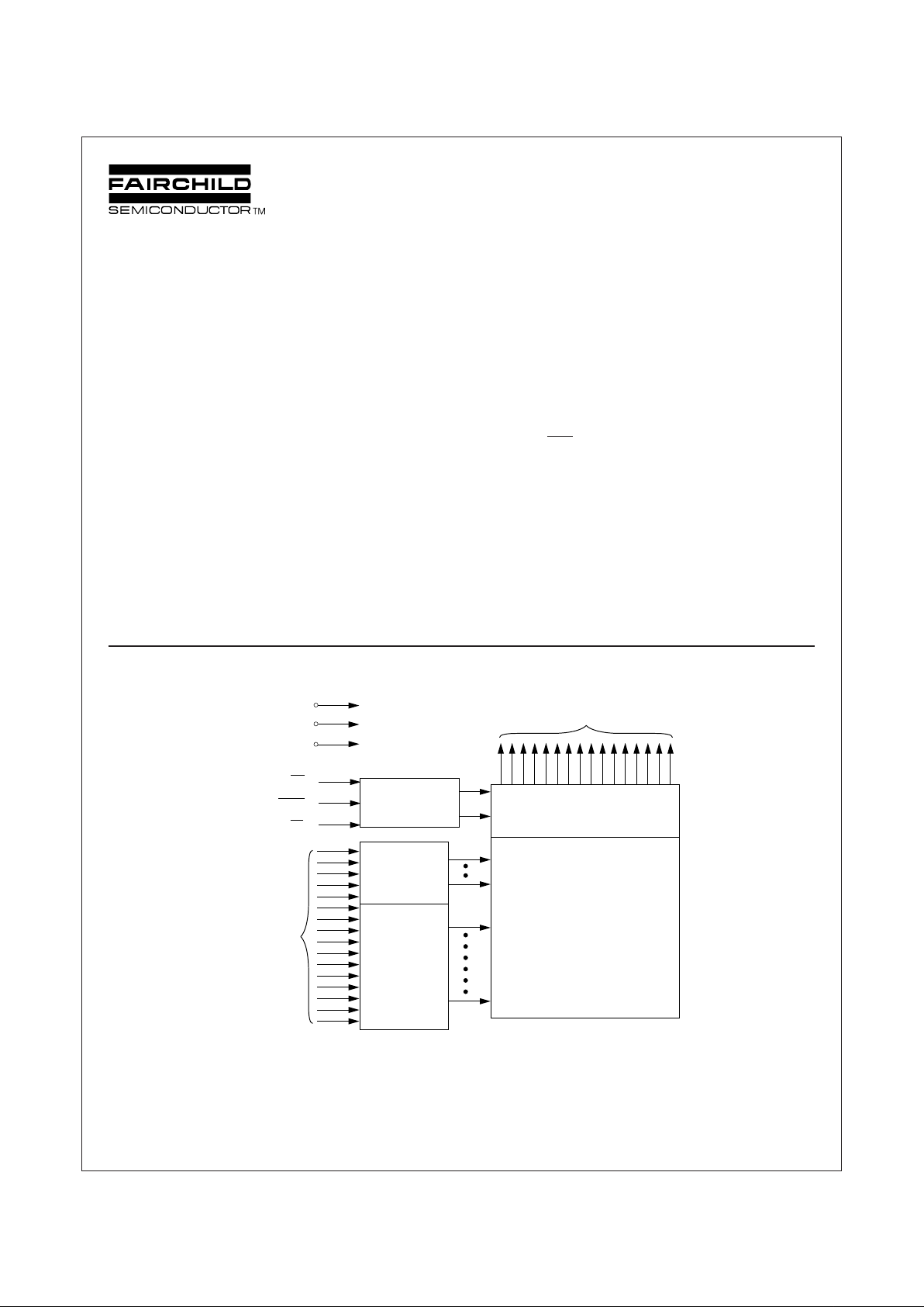
Block Diagram
July 1998
Features
■ High performance CMOS
—90 ns access time
■ Fast turn-off for microprocessor compatibility
■ Simplified upgrade path
—VPP and PGM are “Don’t Care” during normal read
operation
■ Compatible with 27210 and 27C210 EPROMs
■ Manufacturer’s identification code
■ Fast programming
■ JEDEC standard pin configuration
—40-pin CDIP package
—40-pin PDIP package
—44-pin PLCC package
DS011093-1
AMG™ is a trademark of WSI, Inc.
© 1998 Fairchild Semiconductor Corporation
V
cc
GND
V
pp
OE
PGM
CE
Output Enable
Chip Enable, and
Program Logic
Y
Decoder
X
Decoder
Output
Buffers
4,194,304-Bit
Cell Matrix
A
0 - A15
Address
Inputs
Data Outputs O
0 - O15
2
www.fairchildsemi.com
NM27C210 1,048,576-Bit (64K x 16) High Performance CMOS EPROM
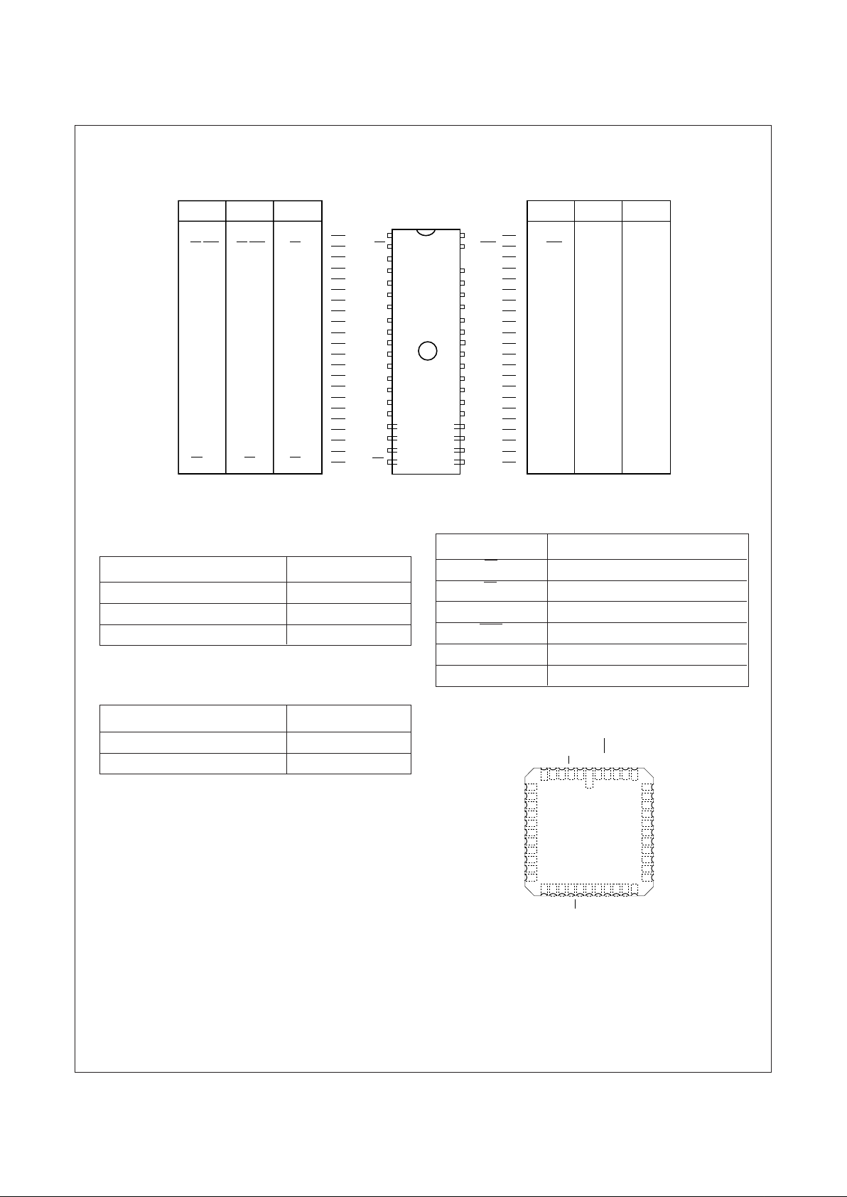
Connection Diagrams
DIP PIN CONFIGURATIONS
Note: Compatible EPROM pin configurations are shown in the blocks adjacent to the NM27C210 pins.
Commercial Temperature Range
(0°C to +70°C) VCC = 5V ±10%
Parameter/Order Number Access Time (ns)
NM27C210 Q, V, N 90 90
NM27C210 Q, V, N 120 120
NM27C210 Q, V, N 150 150
Industrial Temperature Range
(-40°C to +85°C) VCC = 5V ±10%
Parameter/Order Number Access Time (ns)
NM27C210 QE, VE, NE 120 120
NM27C210 QE, VE, NE 150 150
Package Types: NM27C210 Q, V, N XXX
Q = Quartz-Windowed Ceramic DIP package
N = Plastic DIP package
V = PLCC package
• All packages conform to JEDEC standard.
• All versions are guaranteed to function in slower
applications.
Pin Names
A0–A15 Addresses
CE Chip Enable
OE Output Enable
O0–O15 Outputs
PGM Program
XX Don’t Care (During Read)
NC No Connect
PLCC Pin Configuration
27C220 27C240 27C280
A
18
CE/PGM
O
15
O
14
O
13
O
12
O
11
O
10
O
9
O
8
GND
O
7
O
6
O
5
O
4
O
3
O
2
O
1
O
0
OE/V
PP
XXV
PP
CE/PGM
O
15
O
14
O
13
O
12
O
11
O
10
O
9
O
8
GND
O
7
O
6
O
5
O
4
O
3
O
2
O
1
O
0
OE
XXV
PP
CE
O
15
O
14
O
13
O
12
O
11
O
10
O
9
O
8
GND
O
7
O
6
O
5
O
4
O
3
O
2
O
1
O
0
OE
V
CC
A
17
A
16
A
15
A
14
A
13
A
12
A
11
A
10
A
9
GND
A
8
A
7
A
6
A
5
A
4
A
3
A
2
A
1
A
0
V
CC
PGM
A
16
A
15
A
14
A
13
A
12
A
11
A
10
A
9
GND
A
8
A
7
A
6
A
5
A
4
A
3
A
2
A
1
A
0
V
CC
A
17
A
16
A
15
A
14
A
13
A
12
A
11
A
10
A
9
GND
A
8
A
7
A
6
A
5
A
4
A
3
A
2
A
1
A
0
XX/V
PP
CE
O
15
O
14
O
13
O
12
O
11
O
10
O
9
O
8
GND
O
7
O
6
O
5
O
4
O
3
O
2
O
1
O
0
OE
V
CC
XX/PGM
NC
A
15
A
14
A
13
A
12
A
11
A
10
A
9
GND
A
8
A
7
A
6
A
5
A
4
A
3
A
2
A
1
A
0
1
2
3
4
5
6
7
8
9
10
11
12
13
14
15
16
17
18
19
20
40
39
38
37
36
35
34
33
32
31
30
29
28
27
26
25
24
23
22
21
27C280 27C240 27C220
DIP
NM27C210
O
12
O
11
O
10
O
9
O
8
GND
NC
O
7
O
6
O
5
O
4
A
13
A
12
A
11
A
10
A
9
GND
NC
A
8
A
7
A
6
A
5
O13O14O15CE
XX/VPPNC
XX/PGMNCA15A
14
O3O2O1O
0
OE
NC
A1A2A2A3A
4
1
23456
7
8
9
10
11
12
13
14
15
16
17
4041424344
38
37
36
35
34
33
32
31
30
2221201918 282726252423
29
39
V
CC
DS011093-3
DS011093-7
Top View
3
www.fairchildsemi.com
NM27C210 1,048,576-Bit (64K x 16) High Performance CMOS EPROM
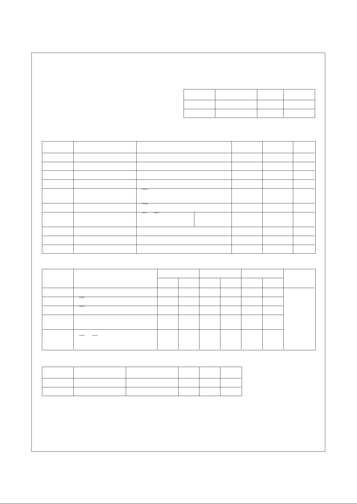
Absolute Maximum Ratings (Note 1)
Storage Temperature -65°C to +150°C
All Input Voltages except A9 with
Respect to Ground (Note 10) -0.6V to +7V
VPP and A9 with Respect to Ground -0.6V to +14V
VCC Supply Voltage with
Respect to Ground -0.6V to +7V
ESD Protection >2000V
All Output Voltages with
Respect to Ground (Note 10) VCC + 1.0V to GND - 0.6V
Operating Range
Range Temperature V
CC
Tolerance
Commercial 0°C to +70°C +5V ±10%
Industrial -40°C to +85°C +5V ±10%
DC Read Characteristics Over Operating Range with V
PP
= V
CC
Symbol Parameter Test Conditions Min Max Units
V
IL
Input Low Level -0.5 0.8 V
V
IH
Input High Level 2.0 VCC +1 V
V
OL
Output Low Voltage IOL = 2.1 mA 0.4 V
V
OH
Output High Voltage IOH = -2.5 mA 3.5 V
I
SB1
VCC Standby Current CE = VCC ± 0.3V 100 µA
(CMOS)
I
SB2
VCC Standby Current CE = V
IH
1mA
ICCVCC Active Current CE = OE = V
IL
f = 5 MHz 40 mA
I/O = 0 mA
I
PP
VPP Supply Current VPP = V
CC
10 µA
I
LI
Input Load Current VIN = 5.5 or GND -1 1 µA
I
LO
Output Leakage Current V
OUT
= 5.5V or GND -10 10 µA
AC Read Characteristics Over Operating Range with V
PP
= V
CC
Symbol Parameter 90 120 150 Units
Min Max Min Max Min Max
t
ACC
Address to Output Delay 90 120 150
t
CE
CE to Output Delay 90 120 150
t
OE
OE to Output Delay 50 50 50
t
DF
Output Disable to Output Float 30 35 45 ns
(Note 2)
t
OH
Output Hold from Addresses,
(Note 2) CE or OE , Whichever 0 0 0
Occurred First
Capacitance (Note 2) T
A
= +25°C, f = 1 MHz
Symbol Parameter Conditions Typ Max Units
C
IN
Input Capacitance VIN = 0V 12 20 pF
C
OUT
Output Capacitance V
OUT
= 0V 13 20 pF
 Loading...