

Fairchild Semiconductor NM27C128N150, NM27C128NE120, NM27C128NE200, NM27C128Q150, NM27C128Q200 Datasheet
...
1
www.fairchildsemi.com
NM27C128 131,072-Bit (16K x 8) High Performance CMOS EPROM
NM27C128
131,072-Bit (16K x 8) High Performance CMOS EPROM
General Description
The NM27C128 is a high performance 128K UV Erasable Electrically Programmable Read Only Memory. It is manufactured with
Fairchild’s latest CMOS split gate EPROM technology which
enables it to operate at speeds as fast as 90 ns access time over
the full operating range.
The NM27C128 provides microprocessor-based systems extensive storage capacity for large portions of operating system and
application software. Its 90 ns access time provides high speed
operation with high-performance CPUs. The NM27C128 offers a
single chip solution for the code storage requirements of 100%
firmware-based equipment. Frequently-used software routines
are quickly executed from EPROM storage, greatly enhancing
system utility.
The NM27C128 is configured in the standard EPROM pinout
which provides an easy upgrade path for systems which are
currently using standard EPROMs.
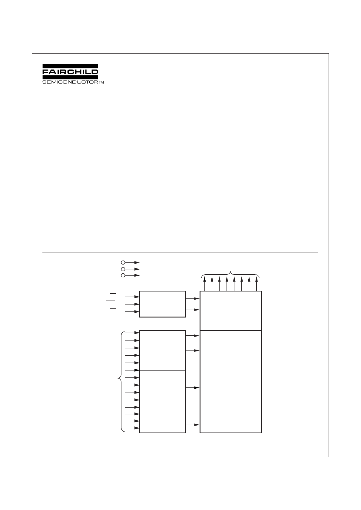
Block Diagram
July 1998
The NM27C128 is one member of a high density EPROM Family
which range in densities up to 4 Mb.
Features
■ High performance CMOS
—90 ns access time
■ Fast turn-off for microprocessor compatibility
■ JEDEC standard pin configuration
—28-pin PDIP package
—32-pin chip carrier
—28-pin CERDIP package
■ Drop-in replacement for 27C128 or 27128
■ 40% faster programming time with Fairchild’s turbo algorithm
© 1998 Fairchild Semiconductor Corporation
Output Enable,
and Chip
Enable Logic
Y Decoder
X Decoder
. . . . . . . . .
Output
Buffers
Y Gating
131,072-Bit
Cell Matrix
Data Outputs O0 - O
7
V
CC
GND
V
PP
OE
PGM
CE
A0 - A
14
Address
Inputs
DS011329-1DS011329-1
2
www.fairchildsemi.com
NM27C128 131,072-Bit (16K x 8) High Performance CMOS EPROM
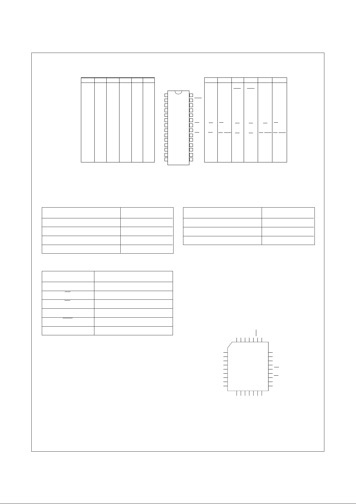
Connection Diagrams
Note: Compatible EPROM pin configurations are shown in the blocks adjacent to the NM27C128 pins.
Commercial Temp. Range
(0°C to +70°C) VCC = 5V ±10%
Parameter/Order Number Access Time (ns)
NM27C128 Q, N, V 90 90
NM27C128 Q, N, V 120 120
NM27C128 Q, N, V 150 150
NM27C128 Q, N, V 200 200
Pin Names
Symbol Description
A0–A13 Addresses
CE Chip Enable
OE Output Enable
O0–O7 Outputs
PGM Program
NC No Connect
Extended Temp. Range
(-40°C to +85°C) V
CC
= 5V ±10%
Parameter/Order Number Access Time (ns)
NM27C128 QE, NE, VE 120 120
NM27C128 QE, NE, VE 150 150
NM27C128 QE, NE, VE 200 200
Note: Surface mount PLCC package available for commercial and extended
temperature ranges only.
Package Types: NM27C128 Q, N, V XXX
Q = Quartz-Windowed Ceramic DIP
N = Plastic OTP DIP
V = Surface-Mount PLCC
• All packages conform to the JEDEC standard.
• All versions are guaranteed to function for slower speeds.
PLCC
Top
1
2
3
4
5
6
7
8
9
10
11
12
13
14
28
27
26
25
24
23
22
21
20
19
18
17
16
15
V
PP
A
12
A
7
A
6
A
5
A
4
A
3
A
2
A
1
A
0
O
0
O
1
O
2
GND
A
19
A
16
A
15
A
12
A
7
A
6
A
5
A
4
A
3
A
2
A
1
A
0
O
0
O
1
O
2
GND
27C080 27C040 27C040
V
PP
A
16
A
15
A
12
A
7
A
6
A
5
A
4
A
3
A
2
A
1
A
0
O
0
O
1
O
2
GND
DlP
NM27C128
V
CC
PGM
A
13
A
8
A
9
A
11
OE
A
10
CE
O
7
O
6
O
5
O
4
O
3
A
15
A
12
A
7
A
6
A
5
A
4
A
3
A
2
A
1
A
0
O
0
O
1
O
2
GND
27C512 27C512
V
PP
A
12
A
7
A
6
A
5
A
4
A
3
A
2
A
1
A
0
O
0
O
1
O
2
GND
27C256 27C256
V
PP
A
16
A
15
A
12
A
7
A
6
A
5
A
4
A
3
A
2
A
1
A
0
O
0
O
1
O
2
GND
27C010
V
PP
A
16
A
15
A
12
A
7
A
6
A
5
A
4
A
3
A
2
A
1
A
0
O
0
O
1
O
2
GND
27C020 27C02027C010
V
CC
PGM
XX
A
14
A
13
A
8
A
9
A
11
OE
A
10
CE
O
7
O
6
O
5
O
4
O
3
27C080
V
CC
A
18
A
17
A
14
A
13
A
8
A
9
A
11
OE/V
PP
A
10
CE/PGM
O
7
O
6
O
5
O
4
O
3
V
CC
A
18
A
17
A
14
A
13
A
8
A
9
A
11
OE
A
10
CE/PGM
O
7
O
6
O
5
O
4
O
3
V
CC
PGM
XX
A
14
A
13
A
8
A
9
A
11
OE
A
10
CE
O
7
O
6
O
5
O
4
O
3
V
CC
A
14
A
13
A8
A
9
A
11
OE
A
10
CE
O
7
O
6
O
5
O
4
O
3
V
CC
A
14
A
13
A
8
A
9
A
11
OE/V
PP
A
10
CE/PGM
O
7
O
6
O
5
O
4
O
3
DS011329-8
DS011329-3
A8
A9
A11
NC
OE
A10
CE
O7
O6
A6
A5
A4
A3
A2
A1
A0
NC
O0
A7
A12
VPPNCVCC
PGM
A13
O1
O2
GND
NC
O3O4O5
5
6
7
8
9
10
11
12
13
29
28
27
26
25
24
23
22
21
14 15 16 17 18 19 20
4 3 2 1 32 31 30
3
www.fairchildsemi.com
NM27C128 131,072-Bit (16K x 8) High Performance CMOS EPROM
Absolute Maximum Ratings (Note 1)
Storage Temperature -65°C to +150°C
All Input Voltages except A9 with
Respect to Ground -0.6V to +7V
VPP and A9 with Respect
to Ground -0.7V to +14V
VCC Supply Voltage with
Respect to Ground -0.6V to +7V
ESD Protection > 2000V
All Output Voltages with
Respect to Ground VCC + 1.0V to GND -0.6V
Operating Range
Range Temperature V
CC
Comm’l 0°C to +70°C +5V ±10%
Industrial -40°C to +85°C +5V ±10%
Read Operation
DC Electrical Characteristics Over Operating Range with V
PP
= V
CC
Symbol Parameter Test Conditions Min Max Units
V
IL
Input Low Level -0.5 0.8 V
V
IH
Input High Level 2.0 VCC +1 V
V
OL
Output Low Voltage IOL = 2.1 mA 0.4 V
V
OH
Output High Voltage IOH = -2.5 mA 3.5 V
I
SB1
VCC Standby Current CE = VCC ±0.3V 100 µA
(CMOS) VIL = GND ± 0.3V, VIH = VCC ±0.3V
I
SB2
VCC Standby Current (T2L) CE = V
IH
1mA
I
CC1
VCC Active Current, T2L Inputs CE = OE = VIL, f = 5 MHz 35 mA
I/O = 0 mA
I
PP
VPP Supply Current VPP = V
CC
10 µA
V
PP
VPP Read Voltage GND V
CC
V
I
LI
Input Load Current VIN = 5.5V or GND -1 1 µA
I
LO
Output Leakage Current V
OUT
= 5.5V or GND -10 10 µA
AC Electrical Characteristics Over Operating Range with V
PP
= V
CC
Symbol Parameter 90 120 150 200 Units
Min Max Min Max Min Max Min Max
t
ACC
Address to Output Delay 90 120 150 200 ns
t
CE
CE to Output Delay 90 120 150 200 ns
t
OE
OE to Output Delay 50 50 50 50 ns
t
CF
CE High to Output Float 30 30 45 55 ns
(Note 2)
t
DF
OE High to Output Float 35 35 45 55 ns
(Note 2)
t
OH
Output Hold from Addresses,
(Note 2) CE or OE, 0000 ns
Whichever Occurred First
4
www.fairchildsemi.com
NM27C128 131,072-Bit (16K x 8) High Performance CMOS EPROM
Capacitance T
A
= +25°C, f = 1 MHz (Note 2)
Symbol Parameter Conditions Typ Max Units
C
IN
Input Capacitance VIN = 0V 6 12 pF
C
OUT
Output Capacitance V
OUT
= 0V 9 12 pF
AC Test Conditions
Output Load 1 TTL Gate and CL = 100 pF (Note 8)
Input Rise and Fall Times ≤ 5 ns
Input Pulse Levels 0.45 to 2.4V
Timing Measurement Reference Level (Note 10)
Inputs 0.8V and 2.0V
Outputs 0.8V and 2.0V
AC Waveforms (Notes 6, 7, 9)
Addresses Valid
Valid Output
Hi-Z
2V
0.8V
2V
0.8V
2V
0.8V
ADDRESSES
OUTPUT
CE
OE
t
CE
2V
0.8V
(Note 3)
(Note 3)
t
DF
t
CF
(Notes 4, 5)
(Notes 4, 5)
t
OH
Hi-Z
t
OE
ACC
t
Note 1: Stresses above those listed under “Absolute Maximum Ratings” may cause permanent damage to the device. This is stress rating only and functional operation of the
device at these or any other conditions above those indicated in the operational sections of this specification is not implied. Exposure to absolute maximum rating conditions for
extended periods may affect device reliability.
Note 2: This parameter is only sampled and is not 100% tested.
Note 3: OE may be delayed up to t
ACC
- tOE after the falling edge of CE without impacting t
ACC
.
Note 4: The tDF and tCF compare level is determined as follows:
High to TRI-STATE®, the measured V
OH1
(DC) - 0.10V;
Low to TRI-STATE, the measured V
OL1
(DC) + 0.10V.
Note 5: TRI-STATE may be attained using OE or CE .
Note 6: The power switching characteristics of EPROMs require careful device decoupling. It is recommended that at least a 0.1 µF ceramic capacitor be used on every device
between VCC and GND.
Note 7: The outputs must be restricted to VCC + 1.0V to avoid latch-up and device damage.
Note 8: TTL Gate: IOL = 1.6 mA, IOH = -400 µA.
CL = 100 pF includes fixture capacitance.
Note 9: VPP may be connected to VCC except during programming.
Note 10:Inputs and outputs can undershoot to -2.0V for 20 ns Max.
DS011329-4
 Loading...