

Fairchild Semiconductor NDM3001 Datasheet
February 1997
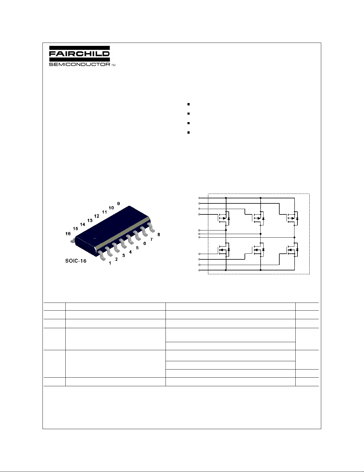
NDM3001
3 Phase Brushless Motor Driver
General Description Features
The NDM3001 three phase brushless motor driver consists of
three N-Channel and P-Channel MOSFETs in a half bridge
configuration. These devices are produced using Fairchild's
proprietary, high cell density DMOS technology. This very high
density process is tailored to minimize on-state resistance
which reduces power loss, provide superior switching
performance, and withstand high energy pulses in the
avalanche and commutation modes. These devices are
particularly suited for low voltage 3 phase motor driver such as
disk drive spindle motor control and other half bridge
applications.
________________________________________________________________________________
±2.9 A, ±30 V, 2.5W
High density cell design for extremely low R
DS(ON)
High power and current handling capability.
Industry standard SOIC-16 surface mount package.
11,14
10
12
15
Q1
.
Q5Q3
1,16
4,13
8,9
Absolute Maximum Ratings T
= 25°C unless otherwise noted
A
2
5
7
3,6
Q2
Q6Q4
Symbol Parameter NDM3001 Units
V
DSS
V
GSS
I
D
Drain-Source Voltage (All Types) ±30 V
Gate-Source Voltage (All Types) ±20 V
Drain Current Q1+Q4 or Q1+Q6 or Q3+Q2 -
±2.9 A
Continuous Q3+Q6 or Q5+Q2 or Q5+Q4
- Pulsed (Note 1a & 2) ±10
P
TJ,T
D
Total Power Dissipation (Note 1a)
Q1+Q4 or Q1+Q6 or Q3+Q2 or (Note 1b)
Q3+Q6 or Q5+Q2 or Q5+Q4
(Note 1c)
Operating and Storage Temperature Range -55 to 150 °C
STG
2.5 W
1.6
1.4
© 1997 Fairchild Semiconductor Corporation
NDM3001 Rev.C
THERMAL CHARACTERISTICS
R
θ
Thermal Resistance, Junction-to-Ambient
JA
Q1+Q4 or Q1+Q6 or Q3+Q2 or
Q3+Q6 or Q5+Q2 or Q5+Q4 (Note 1a)
R
θ
Thermal Resistance, Junction-to-Case
JC
Q1+Q4 or Q1+Q6 or Q3+Q2 or
Q3+Q6 or Q5+Q2 or Q5+Q4 (Note 1)
50 °C/W
20 °C/W
Electrical Characteristics (T
= 25°C unless otherwise noted)
A
Symbol Parameter Conditions Type Min Typ Max Units
OFF CHARACTERISTICS
BV
I
DSS
I
GSS
DSS
Drain-Source Breakdown Voltage
Zero Gate Voltage Drain Current VDS = ±24 V, V
VGS = 0 V, ID = ± 250 µA
= 0 V All ±1 µA
GS
TJ=55oC
Gate - Body Leakage, Forward VGS = ±20 V, VDS = 0 V All ±100 nA
All ±30 V
±10 µA
ON CHARACTERISTICS (Note 3)
V
R
GS(th)
DS(ON)
Gate Threshold Voltage
Static Drain-Source
On-Resistance
VDS = VGS, ID = -250 µA
TJ=125oC
VDS = VGS, ID = 250 µA
TJ=125oC
VGS = -10 V, ID = -2.9 A
TJ=125oC
Q1, Q3, Q5 - 1 -1.6 -2 V
- 0.75 -1.3 -1.5
Q2, Q4, Q6 1 1.5 2
0.75 1.2 1.5
Q1, Q3, Q5 0.19 0.24
0.27 0.45
Ω
VGS = -4.5 V, ID = -2.2 A 0.3 0.36
VGS = 10 V, ID = 2.9 A
Q2, Q4, Q6 0.09 0.115
TJ=125oC 0.126 0.221
0.13 0.16
I
D(on)
VGS = 4.5 V, ID = 2.2 A
On-State Drain Current VGS = 10 V, VDS = -5 V Q1, Q3, Q5 -10 A
VGS = 10 V, VDS = 5 V
Q2, Q4, Q6 10
DYNAMIC CHARACTERISTICS
C
iss
C
oss
Input Capacitance Q1, Q3, Q5
VDS = -15 V, V
f = 1.0 MHz
GS
= 0 V,
Output Capacitance Q1, Q3, Q5 140 pF
Q2, Q4, Q6 VDS =
C
rss
Reverse Transfer Capacitance Q1, Q3, Q5 50 pF
15 V, V
f = 1.0 MHz
GS
= 0 V,
Q1, Q3, Q5 260 pF
Q2, Q4, Q6 185
Q2, Q4, Q6 115
Q2, Q4, Q6 40
NDM3001 Rev.C
Electrical Characteristics (T
= 25°C unless otherwise noted)
A
Symbol Parameter Conditions Type Min Typ Max Units
SWITCHING CHARACTERISTICS
t
t
t
t
D(on)
r
D(off)
f
Turn - On Delay Time Q1, Q3, Q5
Turn - On Rise Time Q1, Q3, Q5 13 40 ns
Turn - Off Delay Time Q1, Q3, Q5 21 90 ns
Turn - Off Fall Time Q1, Q3, Q5 5 50 ns
(Note 3)
V
= -15 V, ID = -1 A,
DD
V
= -10 V, R
GEN
Q2, Q4, Q6
V
= 15 V, ID = 1 A,
DD
V
= 10 V, R
GEN
GEN
GEN
= 6 Ω
= 6 Ω
Q1, Q3, Q5 10 40 ns
Q2, Q4, Q6 9 40
Q2, Q4, Q6 21 40
Q2, Q4, Q6 21 90
Q2, Q4, Q6 8 50
Q
g
Q
gs
Total Gate Charge Q1, Q3, Q5
V
= -10 V,
DS
I
= -3.0 A, VGS = -10 V
Gate-Source Charge Q1, Q3, Q5 1.6 nC
D
Q2, Q4, Q6
V
= 10 V,
Q
gd
Gate-Drain Charge Q1, Q3, Q5 3 nC
DS
I
= 3.0 A, VGS = 10 V
D
Q1, Q3, Q5 10 25 nC
Q2, Q4, Q6 9.5 25
Q2, Q4, Q6 1.5
Q2, Q4, Q6 2.5
DRAIN-SOURCE DIODE CHARACTERISTICS AND MAXIMUM RATINGS
I
S
Maximum Continuous Drain-Source Diode Forward Current Q1, Q3, Q5 -1.2 A
Q2, Q4, Q6 1.2
V
SD
t
rr
Notes:
1. R
design while R
P
Typical R
Drain-Source Diode Forward
Voltage
Reverse Recovery Time
is the sum of the junction-to-case and case-to-ambient thermal resistance where the case thermal reference is defined as the solder mounting surface of the drain pins. R
JA
θ
(t)
D
is determined by the user's board design.
CA
θ
=
JA
θ
a. 50
b. 80
c. 90
T
R
T
J−TA
=
(t)
R
JA
θ
θ
JC
using the board layouts shown below on 4.5"x5" FR-4 PCB in a still air environment:
o
C/W when mounted on a 1 in2 pad of 2oz cpper.
o
C/W when mounted on a 0.027 in2 pad of 2oz cpper.
o
C/W when mounted on a 0.0028 in2 pad of 2oz cpper.
J−TA
+R
2
=I
(t)×R
DS(ON) T
D
(t)
θ
CA
V
= 0 V, IS = -3.0 A
GS
= 0 V, IS = 3.0 A
V
GS
V
= 0 V, I F = ±3.0 A,
GS
dI
/dt = 100 A/µs
F
J
(Note 3)
(Note 3)
1a 1b
Q1, Q3, Q5 -0.8 -1.3 V
Q2, Q4, Q6 0.8 1.3
All 100 ns
is guaranteed by
JC
θ
1c
2. Pulse Test: Pulse Width <
Scale 1 : 1 on letter size paper
300µs, Duty Cycle < 2.0%.
NDM3001 Rev. C
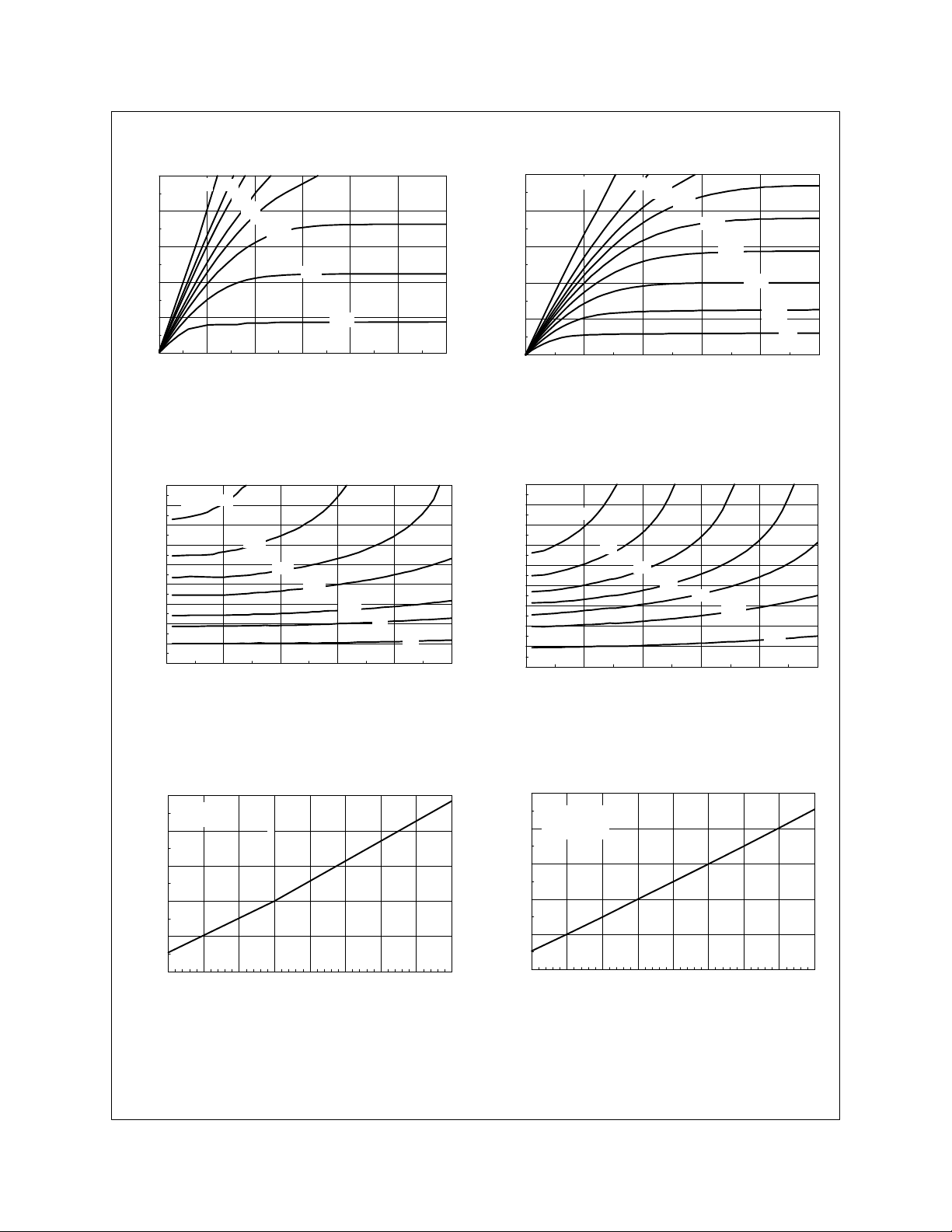
Typical Electrical Characteristics
10
V =10V
GS
8
6
4
2
D
I , DRAIN-SOURCE CURRENT (A)
0
0 0.5 1 1.5 2 2.5 3
Figure 1. N-Channel On-Region Characteristic.
2.6
2.4
2.2
2
1.8
1.6
1.4
DS(on)
R , NORMALIZED
1.2
DRAIN-SOURCE ON-RESISTANCE
1
0.8
0 2 4 6 8 10
V = 3.5V
GS
7.0
6.0
5.0
4.5
4.0
3.5
3.0
V , DRAIN-SOURCE VOLTAGE (V)
DS
4.0
4.5
5.0
6.0
I , DRAIN CURRENT (A)
D
-10
V = -10V
GS
-8
-6
-4
-2
D
I , DRAIN-SOURCE CURRENT (A)
0
-7.0
-6.0
-5.5
-5.0
-4.5
V , DRAIN-SOURCE VOLTAGE (V)
DS
-4.0
-3.5
-3.0
-5-4-3-2-10
Figure 2. P-Channel On-Region
Characteristics.
2.6
2.4
V = -4.0V
GS
2.2
2
1.8
1.6
1.4
7
10
DS(on)
R , NORMALIZED
1.2
DRAIN-SOURCE ON-RESISTANCE
1
0.8
-4.5
-5.0
-5.5
I , DRAIN CURRENT (A)
D
-6.0
-7.0
-10
-10-8-6-4-20
Figure 3. N-Channel On-Resistance Variation with
Gate Voltage and Drain Current.
1.6
ID= 2.9A
VGS= 10V
1.4
1.2
1
DS(ON)
R , NORMALIZED
0.8
DRAIN-SOURCE ON-RESISTANCE
0.6
-50 -25 0 25 50 75 100 125 150
T , JUNCTION TEMPERATURE (°C)
J
Figure 5. N-Channel On-Resistance Variation
with Temperature.
NDM3001 Rev.C
Figure 4. P-Channel On-Resistance Variation
with Gate Voltage and Drain Current.
1.6
I = -2.9A
D
V = -10V
1.4
GS
1.2
1
DS(ON)
R , NORMALIZED
0.8
DRAIN-SOURCE ON-RESISTANCE
0.6
-50 -25 0 25 50 75 100 125 150
T , JUNCTION TEMPERATURE (°C)
J
Figure 6. P-Channel On-Resistance Variation
with Temperature.
 Loading...