

Fairchild Semiconductor NDH8303N Datasheet
NDH8303N
Dual N-Channel Enhancement Mode Field Effect Transistor
General Description Features
May 1997
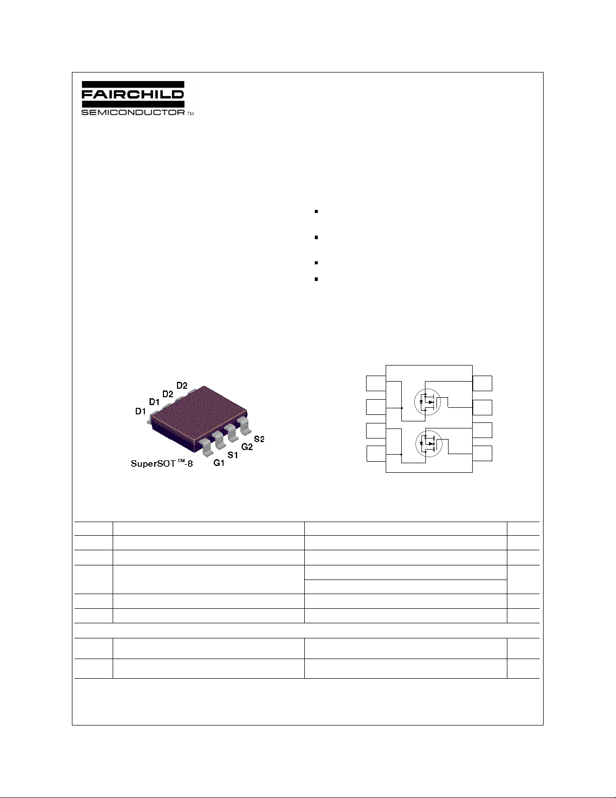
SuperSOTTM-8 N-Channel enhancement mode power field
effect transistors are produced using Fairchild's proprietary,
high cell density, DMOS technology. This very high density
process is especially tailored to minimize on-state resistance.
These devices are particularly suited for low voltage
applications such as notebook computer power management,
and other battery powered circuits where fast switching, and
low in-line power loss are needed in a very small outline surface
mount package.
3.8 A, 20 V. R
R
= 0.035 Ω @ VGS = 4.5 V
DS(ON)
= 0.045 Ω @ VGS = 2.7 V.
DS(ON)
Proprietary SuperSOTTM-8 package design using copper
lead frame for superior thermal and electrical capabilities.
High density cell design for extremely low R
DS(ON)
.
Exceptional on-resistance and maximum DC current
capability.
____________________________________________________________________________________________
5
6
7
8
4
3
2
1
Absolute Maximum Ratings T
= 25°C unless otherwise noted
A
Symbol Parameter NDH8303N Units
V
DSS
V
GSS
I
D
Drain-Source Voltage 20 V
Gate-Source Voltage ±8 V
Drain Current - Continuous (Note 1) 3.8 A
- Pulsed 15
P
D
TJ,T
Maximum Power Dissipation (Note 1) 0.8 W
Operating and Storage Temperature Range -55 to 150 °C
STG
THERMAL CHARACTERISTICS
R
θJA
R
θJC
© 1997 Fairchild Semiconductor Corporation
Thermal Resistance, Junction-to-Ambient (Note 1)
Thermal Resistance, Junction-to-Case (Note 1)
156 °C/W
40 °C/W
NDH8303N Rev.C
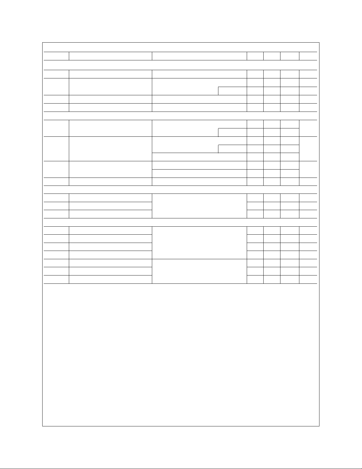
ELECTRICAL CHARACTERISTICS (T
= 25°C unless otherwise noted)
A
Symbol Parameter Conditions Min Typ Max Units
OFF CHARACTERISTICS
BV
I
DSS
DSS
Drain-Source Breakdown Voltage VGS = 0 V, ID = 250 µA 20 V
Zero Gate Voltage Drain Current
VDS = 16 V, V
GS
= 0 V
1 µA
TJ = 55oC 10 µA
I
GSSF
I
GSSR
Gate - Body Leakage, Forward
VGS = 8 V, VDS = 0 V
Gate - Body Leakage, Reverse VGS = -8 V, VDS= 0 V -100 nA
100 nA
ON CHARACTERISTICS (Note 2)
V
GS(th)
Gate Threshold Voltage
VDS = VGS, ID = 250 µA
0.4 0.7 1 V
TJ = 125oC 0.3 0.45 0.8
R
DS(ON)
Static Drain-Source On-Resistance
VGS = 4.5 V, ID = 3.8 A
0.029 0.035
Ω
TJ = 125oC 0.043 0.063
0.036 0.045
5
I
g
D(on)
VGS = 2.7 V, ID = 3.3 A
On-State Drain Current VGS = 4.5 V, VDS = 5 V 15 A
VGS = 2.7 V, VDS = 5 V
FS
Forward Transconductance VDS = 5 V, ID = 3.8 A 15 S
DYNAMIC CHARACTERISTICS
C
iss
C
oss
C
rss
Input Capacitance
Output Capacitance 370 pF
VDS = 10 V, VGS = 0 V,
f = 1.0 MHz
Reverse Transfer Capacitance 145 pF
700 pF
SWITCHING CHARACTERISTICS (Note 2)
t
t
t
t
Q
Q
Q
D(on)
r
D(off)
f
g
gs
gd
Turn - On Delay Time VDD = 5 V, ID = 1 A,
Turn - On Rise Time 22 40 ns
VGS = 4.5 V, R
GEN
= 6 Ω
8 15 ns
Turn - Off Delay Time 48 90 ns
Turn - Off Fall Time 23 40 ns
Total Gate Charge VDS = 10 V,
Gate-Source Charge 2.5 nC
ID = 3.8 A, VGS = 4.5 V
19.6 nC
Gate-Drain Charge 6.5 nC
NDH8303N Rev.C
 Loading...