

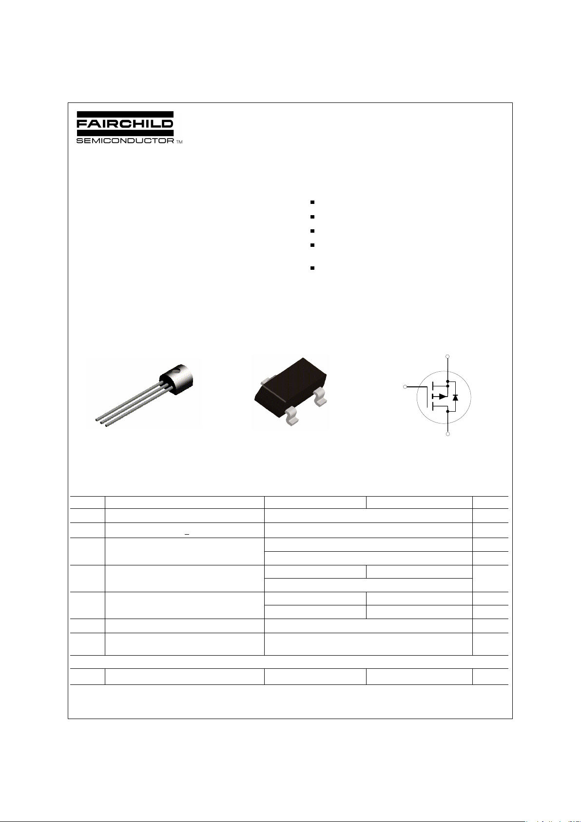
Fairchild Semiconductor NDF0610 Datasheet
April 1995
NDF0610 / NDS0610
P-Channel Enhancement Mode Field Effect Transistor
General Description Features
____________________________________________________________________________________________
NDF0610
Absolute Maximum Ratings T
A
= 25°C unless otherwise noted
Symbol Parameter NDF0610 NDS0610 Units
V
DSS
Drain-Source Voltage -60 V
V
DGR
Drain-Gate Voltage (RGS < 1 MΩ)
-60 V
V
GSS
Gate-Source Voltage - Continuous ±20 V
- Nonrepetitive (tP < 50 µs) ±30 V
I
D
Drain Current - Continuous -0.18 -0.12 A
- Pulsed -1
P
D
Maximum Power Dissipation TA = 25°C 0.8 0.36 W
Derate above 25°C 5 2.9 mW/oC
TJ,T
STG
Operating and Storage Temperature Range -55 to 150 °C
T
L
Maximum lead temperature for soldering
purposes, 1/16" from case for 10 seconds
300 °C
THERMAL CHARACTERISTICS
R
θ
JA
Thermal Resistance, Junction-to-Ambient 200 350 °C/W
NDS0610.SAM
These P-Channel enhancement mode power field effect
transistors are produced using Fairchild's proprietary, high
cell density, DMOS technology. This very high density
process has been designed to minimize on-state resistance,
provide rugged and reliable performance and fast switching.
They can be used, with a minimum of effort, in most
applications requiring up to 180mA DC and can deliver
pulsed currents up to 1A. This product is particularly suited
to low voltage applications requiring a low current high side
switch.
-0.18 and -0.12A, -60V. R
DS(ON)
= 10Ω
Voltage controlled p-channel small signal switch
High density cell design for low R
DS(ON)
TO-92 and SOT-23 packages for both through hole and
surface mount applications
High saturation current
G
D
S
SOT-23
NDS0610
S
D
G
© 1998 Fairchild Semiconductor Corporation
S
G
D
TO-92
ELECTRICAL CHARACTERISTICS (T
A
= 25°C unless otherwise noted)
Symbol Parameter Conditions Min Typ Max Units
OFF CHARACTERISTICS
BV
DSS
Drain-Source Breakdown Voltage VGS = 0 V, ID = -10 µA -60 V
I
DSS
Zero Gate Voltage Drain Current VDS = -48 V, V
GS
= 0 V -1 µA
T
J
= 125°C -200 µA
I
GSSF
Gate - Body Leakage, Forward VGS = 20 V, VDS = 0 V 10 nA
I
GSSR
Gate - Body Leakage, Reverse VGS = -20 V, VDS= 0 V -10 nA
ON CHARACTERISTICS (Note 1)
V
GS(th)
Gate Threshold Voltage V
DS
= V
GS
, I
D
= -1 mA -1 -2.4 -3.5 V
T
J
= 125°C -0.6 -2.1 -3.2
R
DS(ON)
Static Drain-Source On-Resistance VGS = -10 V, ID = -0.5 A 3.6 10
Ω
T
J
= 125°C 5.9 16
VGS = -4.5 V, ID = -0.25 A 5.2 20
T
J
= 125°C 7.9 30
I
D(on)
On-State Drain Current VGS = -10 V, VDS = -10 V -0.6 -1.6 A
VGS = -4.5 V, VDS = -10 V -0.35
g
FS
Forward Transconductance VDS = -10 V, ID = -0.1 A 70 170 mS
DYNAMIC CHARACTERISTICS
C
iss
Input Capacitance VDS = -25 V, VGS = 0 V,
f = 1.0 MHz
40 60 pF
C
oss
Output Capacitance 11 25 pF
C
rss
Reverse Transfer Capacitance 3.2 5 pF
SWITCHING CHARACTERISTICS (Note 1)
t
D(on)
Turn - On Delay Time VDD = -25 V, ID = -0.18 A,
VGS = -10 V, R
GEN
= 25 Ω
7 10 nS
t
r
Turn - On Rise Time 5 15 nS
t
D(off)
Turn - Off Delay Time 13 15 nS
t
f
Turn - Off Fall Time 10 20 nS
Q
g
Total Gate Charge VDS = -48 V,
ID = -0.5 A, VGS = -10 V
1.43 nC
Q
gs
Gate-Source Charge 0.6 nC
Q
gd
Gate-Drain Charge 0.25 nC
DRAIN-SOURCE DIODE CHARACTERISTICS
I
S
Maximum Continuous Source Current -0.18 A
I
SM
Maximum Pulse Source Current (Note 1) -1 A
V
SD
Drain-Source Diode Forward Voltage
VGS = 0 V, IS = -0.5 A
(Note 1)
-1.2 -1.5 V
TJ = 125°C -0.98 -1.3
t
rr
Reverse Recovery Time VGS = 0 V, IS = -0.5 A,
dIF/dt = 100 A/µs
40 ns
I
rr
Reverse Recovery Current 2.8 A
Note:
1. Pulse Test: Pulse Width < 300 µs, Duty Cycle < 2.0%.
NDS0610.SAM
NDS0610.SAM
-10-8-6-4-20
-1.4
-1.2
-1
-0.8
-0.6
-0.4
-0.2
0
V , DRAIN-SOURCE VOLTAGE (V)
I , DRAIN-SOURCE CURRENT (A)
V = -10V
GS
DS
D
-8
-7
-6
-5
-4
-9
-50 -25 0 25 50 75 100 125 150
0.6
0.8
1
1.2
1.4
1.6
1.8
T , JUNCTION TEMPERATURE (°C)
DRAIN-SOURCE ON-RESISTANCE
J
R , NORMALIZED
DS(ON)
I = -0.5A
V = -10V
D
GS
-50 -25 0 25 50 75 100 125 150
0.8
0.85
0.9
0.95
1
1.05
1.1
T , JUNCTION TEMPERATURE (°C)
GATE-SOURCE THRESHOLD VOLTAGE
J
V = V
I = -1mA
D
DS GS
V , NORMALIZED
th
-1.4-1.2-1-0.8-0.6-0.4-0.20
0.5
1
1.5
2
2.5
3
I , DRAIN CURRENT (A)
DRAIN-SOURCE ON-RESISTANCE
T = 125°C
J
-55
D
R , NORMALIZED
DS(on)
125
25
-55
V
-4.5V
-10V
GS
25
Typical Electrical Characteristics
Figure 1. On-Region Characteristics
Figure 2. On-Resistance Variation with Gate
Voltage and Drain Current
Figure 3. On-Resistance Variation
with Temperature
Figure 4. On-Resistance Variation with Drain
Current and Temperature
Figure 5. Transfer Characteristics
Figure 6. Gate Threshold Variation with
Temperature
-10-8-6-4-20
-1.2
-1
-0.8
-0.6
-0.4
-0.2
0
V , GATE TO SOURCE VOLTAGE (V)
I , DRAIN CURRENT (A)
25
125
V = -10V
DS
GS
D
T = -55°C
J
-1.4-1.2-1-0.8-0.6-0.4-0.20
0.8
1
1.2
1.4
1.6
1.8
2
2.2
I , DRAIN CURRENT (A)
DRAIN-SOURCE ON-RESISTANCE
V = -4V
GS
D
R , NORMALIZED
DS(on)
-5
-7
-8
-9
-10
-6
NDS0610.SAM
-50 -25 0 25 50 75 100 125 150
0.9
0.95
1
1.05
1.1
1.15
T , JUNCTION TEMPERATURE (°C)
DRAIN-SOURCE BREAKDOWN VOLTAGE (V)
I = -10µA
D
BV , NORMALIZED
DSS
J
0.6 0.8 1 1.2 1.4 1.6 1.8
0.1
0.2
0.3
0.5
1
1.5
-V , BODY DIODE FORWARD VOLTAGE (V)
-I , REVERSE DRAIN CURRENT (A)
V = 0V
GS
T = 125°C
J
25
-55
SD
S
0 0.2 0.4 0.6 0.8 1 1.2 1.4 1.6
-10
-8
-6
-4
-2
0
Q , GATE CHARGE (nC)
V , GATE-SOURCE VOLTAGE (V)
g
GS
-48
V = -12V
DS
I = -0.5A
D
-24
0.1 0.2 0.5 1 2 5 10 20 30 60
2
3
5
10
20
30
50
70
-V , DRAIN TO SOURCE VOLTAGE (V)
CAPACITANCE (pF)
DS
C
iss
f = 1 MHz
V = 0V
GS
C
oss
C
rss
-1.4-1.2-1-0.8-0.6-0.4-0.20
0
0.1
0.2
0.3
0.4
I , DRAIN CURRENT (A)
g , TRANSCONDUCTANCE (SIEMENS)
T = -55°C
J
25
D
FS
V = -10V
DS
125
Figure 7. Breakdown Voltage Variation with
Temperature
Figure 8. Body Diode Forward Voltage
Variation with Current and Temperature
Figure 9. Capacitance Characteristics Figure 10. Gate Charge Characteristics
Figure 11. Transconductance Variation with Drain
Current and Temperature
Typical Electrical Characteristics (continued)
 Loading...