

Fairchild Semiconductor NDC7003P Datasheet
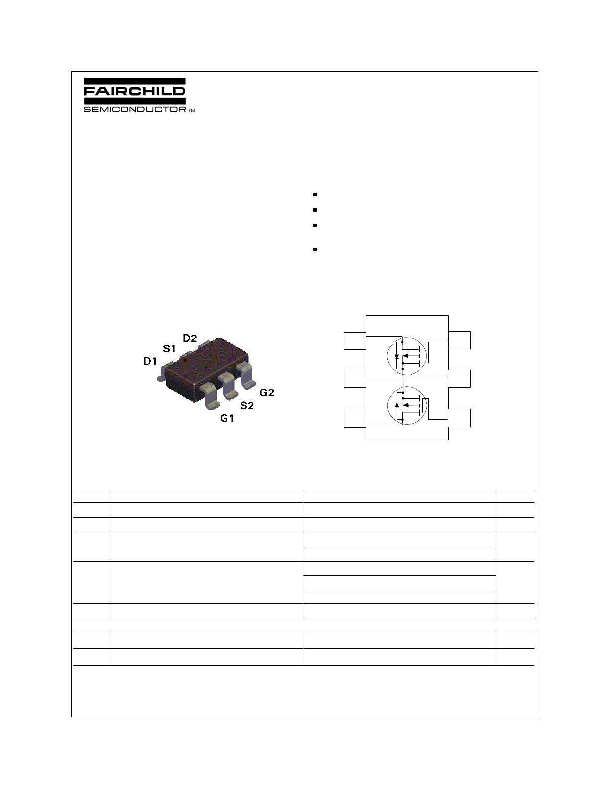
NDC7003P
Dual P-Channel Enhancement Mode Field Effect Transistor
General Description Features
March 1996
These dual P-Channel enhancement mode power field
effect transistors are produced using Fairchild's
proprietary, high cell density, DMOS technology. This
very high density process has been designed to minimize
on-state resistance, provide rugged and reliable
performance and fast switching. This product is
particularly suited to low voltage applications requiring a
low current high side switch.
-0.34A, -50V. R
High density cell design for low R
= 5Ω @ VGS=-10V.
DS(ON)
DS(ON)
.
Proprietary SuperSOTTM-6 package design using copper
lead frame for superior thermal and electrical capabilities.
High saturation current.
____________________________________________________________________________________________
4
5
6
3
2
1
SOT-6 (SuperSOTTM-6)
Absolute Maximum Ratings T
= 25°C unless otherwise noted
A
Symbol Parameter NDC7003P Units
V
DSS
V
GSS
I
D
Drain-Source Voltage -50 V
Gate-Source Voltage - Continuous -20 V
Drain Current - Continuous (Note 1a) -0.34 A
- Pulsed -1
P
D
TJ,T
Maximum Power Dissipation (Note 1a) 0.96 W
(Note 1b)
(Note 1c)
Operating and Storage Temperature Range -55 to 150 °C
STG
0.9
0.7
THERMAL CHARACTERISTICS
R
θ
R
θ
© 1997 Fairchild Semiconductor Corporation
Thermal Resistance, Junction-to-Ambient (Note 1a) 130 °C/W
JA
Thermal Resistance, Junction-to-Case (Note 1) 60 °C/W
JC
ELECTRICAL CHARACTERISTICS (T
= 25°C unless otherwise noted)
A
Symbol Parameter Conditions Min Typ Max Units
OFF CHARACTERISTICS
BV
I
DSS
DSS
Drain-Source Breakdown Voltage VGS = 0 V, ID = -250 µA -50 V
Zero Gate Voltage Drain Current
VDS = -40 V, V
GS
= 0 V
-1 µA
TJ = 125°C -500
I
GSSF
I
GSSR
Gate - Body Leakage, Forward
VGS = 20 V, VDS = 0 V
Gate - Body Leakage, Reverse VGS = -20 V, VDS= 0 V -100 nA
100 nA
ON CHARACTERISTICS (Note 2)
V
GS(th)
Gate Threshold Voltage
VDS = VGS, ID = -250 µ.A
-1 -2.5 -3.5 V
TJ = 125°C -0.8 -2.2 -3
R
DS(ON)
Static Drain-Source On-Resistance
VGS = -10 V, ID = -0.34 A
2.5 5
Ω
TJ = 125°C 4 10
5.3 7.5
250 mS
I
g
D(on)
VGS = -4.5 V, ID = -0.25 A
On-State Drain Current VGS = -10 V, VDS = -10 V -1 A
FS
Forward Transconductance
VDS = -10 V, ID = -0.34 A
DYNAMIC CHARACTERISTICS
C
iss
C
oss
C
rss
Input Capacitance VDS = -25 V, VGS = 0 V,
Output Capacitance 13 pF
f = 1.0 MHz
Reverse Transfer Capacitance 4 pF
40 pF
SWITCHING CHARACTERISTICS (Note 2)
t
t
t
t
Q
Q
Q
D(on)
r
D(off)
f
g
gs
gd
Turn - On Delay Time VDD = -25 V, ID = -0.25 A,
Turn - On Rise Time 6 20
VGS = -10 V, R
GEN
= 25 Ω
14 20 nS
Turn - Off Delay Time 13 20
Turn - Off Fall Time 6 20
Total Gate Charge VDS = -25 V,
Gate-Source Charge 0.23 nC
ID = -0.34 A, VGS = -10 V
1.3 nC
Gate-Drain Charge 0.38 nC
ELECTRICAL CHARACTERISTICS (T
= 25°C unless otherwise noted)
A
Symbol Parameter Conditions Min Typ Max Units
DRAIN-SOURCE DIODE CHARACTERISTICS
I
S
I
SM
V
SD
Notes:
1. R
P
design while R
Typical R
Maximum Continuous Source Current -0.34 A
Maximum Pulse Source Current (Note 2) -1 A
Drain-Source Diode Forward Voltage VGS = 0 V, IS = -0.34 A (Note 2) -0.8 -1.2 V
is the sum of the junction-to-case and case-to-ambient thermal resistance where the case thermal reference is defined as the solder mounting surface of the drain pins. R
JA
θ
(t)
D
is determined by the user's board design.
CA
θ
T
=
R
θ
a. 130oC/W when mounted on a 0.125 in2 pad of 2oz cpper.
b. 140oC/W when mounted on a 0.005 in2 pad of 2oz cpper.
c. 180oC/W when mounted on a 0.0015 in2 pad of 2oz cpper.
T
J−TA
=
(t)
R
θJ A
θ
J C
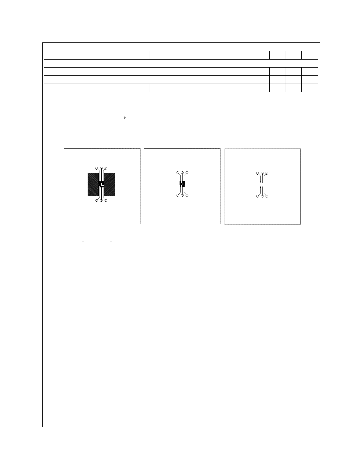
for single device operation using the board layouts shown below on 4.5"x5" FR-4 PCB in a still air environment:
JA
J−TA
+R
2
= I
(t) × R
DS(ON ) T
D
(t)
θ
CA
J
1a 1b
1c
is guaranteed by
JC
θ
Scale 1 : 1 on letter size paper
2. Pulse Test: Pulse Width < 300µs, Duty Cycle < 2.0%.
 Loading...