

Fairchild Semiconductor NC7WZU04 Datasheet
NC7WZU04
NC7WZU04 TinyLogic
March 1999
Revised May 2003
TinyLogic
General Description
The NC7WZU04 is a dual unbuffered inverter from
Fairchild’s Ultra High Speed Series of TinyLogic
space saving SC70 6 -lead package. The special purpose
unbuffered circuit design is intended for crystal oscillator or
analog applications. The device is fabricated with
advanced CMOS technolog y to achieve ultra high speed
with high output drive while maintaining low static power
dissipation over a very broad V
device is specified to o perate over the 1.65V to 5.5V V
range. The inputs are high impedance when VCC is 0V.
Inputs tolerate voltages up to 7V inde pe nde nt o f V
ating voltage.
UHS Dual Unbuffered Inverter
Features
in the
operating range. The
CC
CC
oper-
■ Space saving SC70 6-lead package
■ Ultra small MicroPak
■ Unbuffered for crystal oscillator and analog applications
■ Balanced Output Drive:
■ Broad VCC Operating Range: 1.65V to 5.5V
■ Low Quiescent Power: I
CC
leadless package
±8 mA at 4.5V V
< 1 µA at 5V VCC, TA = 25°C
CC
CC
Ordering Code:
Order Package Product Code
Number Number Top Mark
NC7WZU04P6X MAA06A ZU4 6-Lead SC70, EIAJ SC88, 1.25mm Wide 3k Units on Tape and Reel
NC7WZU04L6X MAC06A B5 6-Lead MicroPak, 1.0mm Wide 5k Units on Tape and Reel
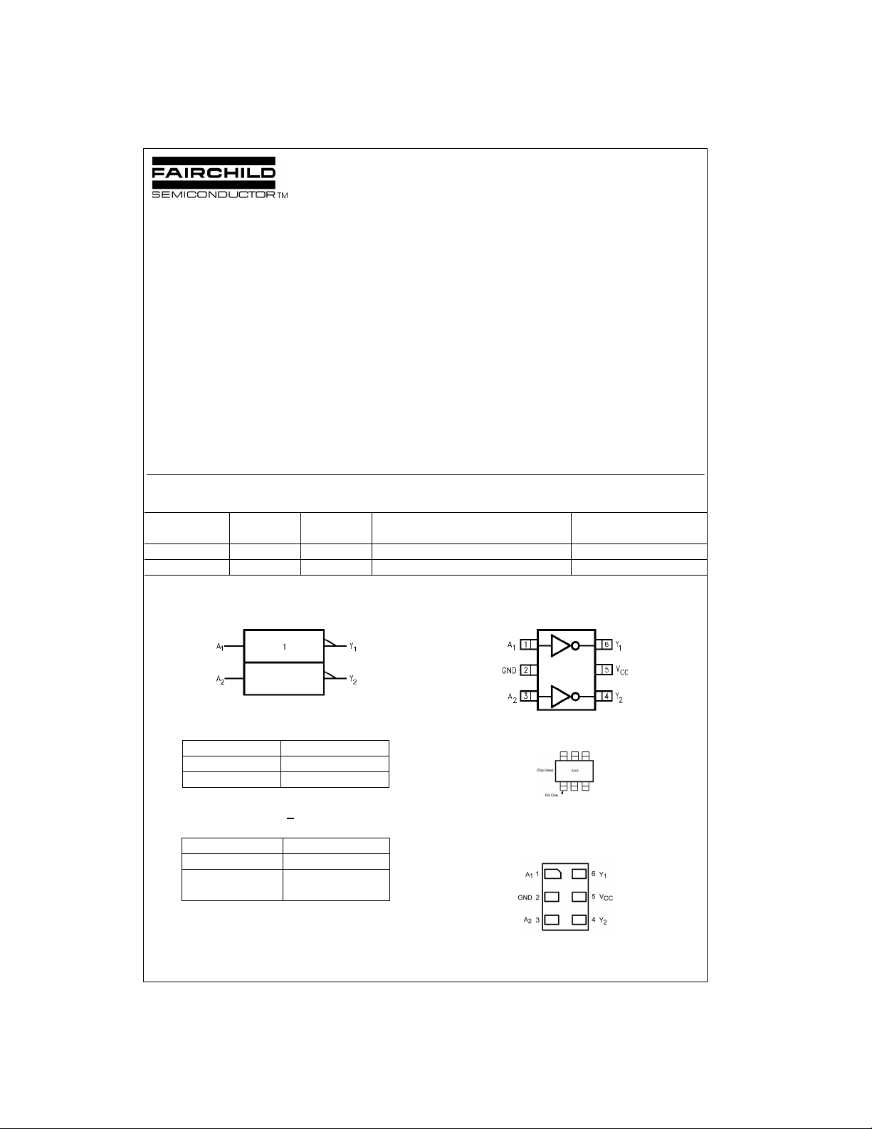
Logic Symbol
IEEE/IEC
Package Descript ion Supplied As
Connection Diagrams
Pin Assignments for SC 70
UHS Dual Unbuffered Inverter
Pin Descriptions
Pin Names Description
, A
A
1
2
Y
, Y
1
2
Function Table
Input Output
AY
LH
HL
H = HIGH Logic Le v el
L = LOW Logic Level
TinyLogic is a registered trademark of F airc hild Semiconduct or Corporation.
MicroPak is a tradem ark of Fairchild Semiconductor Corporation.
© 2003 Fairchild Semiconductor Corporation DS500220 www.fairchildsemi.com
Y = A
Data Inputs
Output
AAA represents Product Code Top Mark - see ordering code
Note: Orientation of Top Mark determines Pin On e locat ion. R ead the Top
Product Code Mark left to right, Pin One is the lower left pin (see diagram).
Pin One Orientation Diagram
Pad Assignments for MicroPak
(Top View)

Connection Diagrams (Continued)
(Top Thru View)
NC7WZU04
www.fairchildsemi.com 2
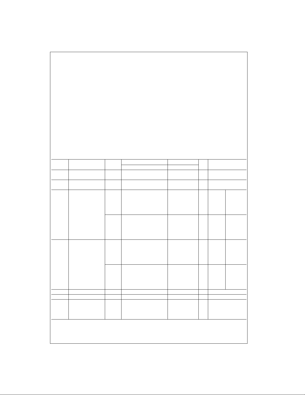
Absolute Maximum Ratings(Note 1) Recommended Operating
Supply Voltage (VCC) −0.5V to +7V
DC Input Voltage (V
DC Output Voltage (V
DC Input Diode Current (I
V
< −0.5V −50 mA
IN
DC Output Diode Current (I
< −0.5V −50 mA
V
OUT
V
> 0.5V, VCC = GND +50 mA
OUT
DC Output Current (I
/GND Current (ICC/I
DC V
CC
Storage Temperature (T
Junction Temperature under Bias (T
Junction Lead Temperature (T
) −0.5V to +7V
IN
) −0.5V to +7V
OUT
)
IK
)
OK
) ±50 mA
OUT
) ±100 mA
GND
) −65°C to +150°C
STG
) 150°C
J
)
L
(Soldering, 10 seconds) 260
Power Dissipation (P
) @ +85°C 180 mW
D
Conditions
Supply Voltage Operating (V
Supply Voltage Data Retention (V
Input Voltage (V
Output Voltage (V
Operating Temperature (TA) −40°C to +85°C
Thermal Resistance (
Note 1: Absolute maximum ratings are DC values beyond which t he devi ce
may be damag ed or hav e it s usefu l li fe i mpa ired. Th e da tas heet sp ecific ations should be met, without exception, to ensure that the system design is
reliable over its power supply, temperature, and output/input loading variables. Fairchild does not recommend operation outside datasheet specifications.
Note 2: Unused inputs must be held HIGH or LOW. They may not float.
°C
(Note 2)
) 1.8V to 5.5V
CC
) 1.5V to 5.5V
) 0V to 5.5V
IN
)0V to V
OUT
θ
JA
CC
)350°C/W
DC Electrical Characteristics
Symbol Parameter
V
IH
V
IL
V
OH
V
OL
I
IN
I
CC
I
CCPEAK
HIGH Level 1.8 to 2.7 0.85 V
Input Voltage 3.0 to 5.5 0.8 V
LOW Level 1.8 to 2.7 0.15 V
Input Voltage 3.0 to 5.5 0.2 V
HIGH Level 1.65 1.55 1.65 1.55
Output Voltage 1.8 1.6 1.79 1.6
LOW Level 1.65 0.01 0.2 0.2
Output Voltage 1.8 0.01 0.2 0.2
Input Leakage Current 0 to 5.5 ±0.1 ±1.0 µAVIN = 5.5V, GND
Quiescent Supply Current 1.65 to 5.5 1.0 10 µAVIN = 5.5V, GND
Peak Supply Current 1.8 0.2
in Analog Operation 2.5 2 VIN = Adjust for
V
CC
(V) Min Typ Max Min Max
2.3 2.1 2.29 2.1
3.0 2.7 2.99 2.7
4.5 4.0 4.48 4.0
1.65 1.26 1.52 1.29
2.3 1.9 2.19 1.9 I
3.0 2.4 2.82 2.4 IOH = −4mA
3.0 2.3 2.73 2.3 I
4.5 3.8 4.24 3.8 I
2.3 0.01 0.2 0.2
3.0 0.01 0.3 0.3
4.5 0.01 0.5 0.5
1.65 0.10 0.24 0.24
2.3 0.12 0.3 0.3 IOL =2 mA
3.0 0.19 0.4 0.4 IOL = 4mA
3.0 0.29 0.55 0.55 IOL = 6 mA
4.5 0.29 0.55 0.55 IOL = 8 mA
3.3 5 Peak ICC Current
5.0 15
TA = +25°CT
CC
CC
A
0.85 V
0.8 V
CC
CC
= −40°C to +85°C
CC
CC
0.15 V
0.2 V
CC
Units Conditions
V
CC
V
VVIN = VILIOH = −100 µA
VVIN = GND
VVIN = VIHIOL = 100 µA
VVIN = V
V
OUT
mA
CC
= Open
I
= −2 mA
OH
= −2 mA
OH
= −6 mA
OH
= −8 mA
OH
IOL =2 mA
NC7WZU04
CC
3 www.fairchildsemi.com
 Loading...