

Fairchild Semiconductor ISL9N2357D3ST Datasheet
Data Sheet June 2002
ISL9N2357D3ST
30V, 0.007 Ohm, 35A, N-Channel
UltraFET
UltraFET® Trench from Fairchild is a new advanced
MOSFET technology that achieves the lowest possible onresistance per silicon area while maintaining fast switching
and low gat e charge. The reduced c onduction and s wi tching
losses extend battery life in notebook PCs, cellular
telephones and other portable information appliances and
improve the overall efficiency of high frequency DC-DC
converters used to power the latest microprocessors.
®
Trench Power MOSFET
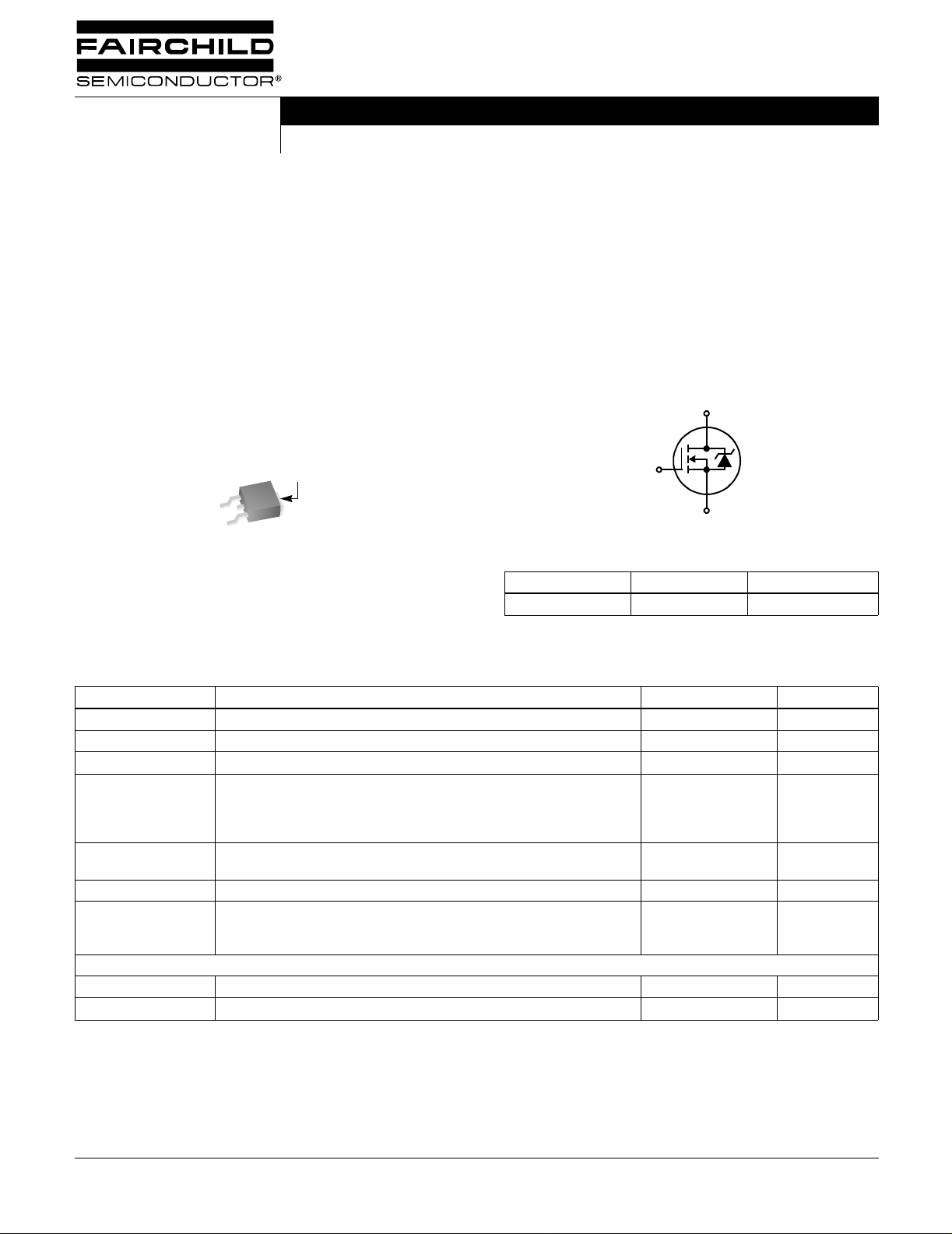
Packaging
ISL9N2357D3ST
JEDEC TO-252AA
DRAIN (FLANGE)
GATE
SOURCE
UltraFET® Trench
Features
•r
•Q
•Q
•C
Symbol
Ordering Information
ISL9N2357D3ST TO-252AA N2357D
NOTE: When ordering, use the entire part number.
e.g., ISL9N2357D3ST.
= 0.006Ω Typical, V
DS(ON)
Total 85nC Typical, VGS = 10V
g
16nC Typical
gd
5600pF Typical
ISS
G
PART NUMBER PACKAGE BRAND
D
S
GS
= 10V
Absolute Maximum Ratings T
SYMBOL PARAMETER ISL9N2357D3ST UNITS
V
DSS
V
DGR
V
GS
I
D
I
D
I
DM
P
D
T
, T
J
STG
T
L
T
pkg
THERMAL SPECI FICATIONS
R
θJC
R
θJA
NOTE:
1. T
= 25oC to 150oC.
J
CAUTION: Stresses above those listed in “ Absolute M aximum Ratings” may cause perm anent damage to the device. This is a stre ss only rating and operation of the
device at these or any other conditions above those indicated in the operational sections of this specification is not implied.
Drain to Source Voltage (Note 1) 30 V
Drain to Gate Voltage (RGS = 20kΩ) (Note 1) 30 V
Gate to Source Voltage ±20 V
Drain Current
Continuous (T
Continuous (T
Pulsed Drain Current
Power Dissipation
Derate Above 25
Operating and Storage Temperature -55 to 175
Maximum Temperature for Soldering
Leads at 0.063in (1.6mm) from Case for 10s
Package Body for 10s, See Techbrief TB334
Thermal Resistance Junction to Case, TO-252 1.5
Thermal Resistance Junction to Ambient TO-252 100
= 25oC, Unless Otherwise Specified
C
= 25oC, VGS = 10V) (Figure 2)
C
= 100oC, VGS = 10V)
C
o
C
35
35
Figure 4
100
0.67
300
260
A
A
A
W
W/oC
o
C
o
C
o
C
o
C/W
o
C/W
©2002 Fairchild Semiconductor Corporation ISL9N2357D3ST Rev. B1

ISL9N2357D3ST
Electrical Specifications T
= 25oC, Unless Otherwise Specified
C
PARAMETER SYMBOL TEST CONDITIONS MIN TYP MAX UNITS
OFF STATE SPECIFICATIONS
Drain to Source Breakdown Voltage BV
Zero Gate Voltage Drain Current I
Gate to Source Leakage Current I
ON STATE SPECIFICATIONS
Gate to Source Threshold Voltage V
Drain to Source ON Resistance r
SWITCHING SPECIFICATIONS (V
GS
= 10V)
Turn-On Time t
Turn-On Delay Time t
Rise Time t
Turn-Off Delay Time t
Fall Time t
Turn-Off Time t
GATE CHARGE SPECIFICATIONS
Total Gate Charge at 20V Q
Total Gate Charge at 10V Q
Threshold Gate Charge Q
Gate to Source Gate Charge Q
Gate to Drain “Miller” Charge Q
CAPACITANCE SPECIFICATIONS
Input Capacitance C
Output Capacitance C
Reverse Transfer Capacitance C
DSSID
DSS
GSS
GS(TH)VGS
DS(ON)ID
ON
d(ON)
d(OFF)
OFF
g(TOT)VGS
g(10)
g(TH)
ISS
VDS = 25V, VGS = 0V - - 1 µA
V
DS
VGS = ±20V - - ±100 nA
VDD = 15V, ID = 20A
V
GS
R
GS
(Figures 14, 15)
r
f
VGS = 0V to 10V - 85 130 nC
VGS = 0V to 2V - 11 17 nC
gs
gd
VDS = 25V, VGS = 0V,
f = 1MHz
OSS
RSS
(Figure 10)
= 250µA, VGS = 0V (Figure 9) 30 - - V
= 25V, VGS = 0V, TC = 150oC - - 250 µA
= VDS, ID = 250µA (Figure 8) 2 - 4 V
= 35A, VGS = 10V (Figure 7) - 0.006 0.007 Ω
- - 144 ns
= 10V,
= 9.1Ω
-27-ns
-69-ns
-84-ns
-53-ns
- - 207 ns
= 0V to 20V VDD = 15V,
I
= 20A,
D
= 1.0mA
I
g(REF)
(Figures 11, 12, 13)
- 172 258 nC
-23-nC
-16-nC
- 5600 - pF
- 526 - pF
- 355 - pF
Source to Drain Diode Specifications
PARAMETER SYMBOL TEST CONDITIONS MIN TYP MAX UNITS
I
Source to Drain Diode Voltage V
Reverse Recovery Time t
Reverse Recovered Charge Q
©2002 Fairchild Semiconductor Corporation ISL9N2357D3ST Rev. B1
SD
rr
RR
= 20A - - 1.25 V
SD
I
= 10A - - 1.0 V
SD
ISD = 20A, dISD/dt = 100A/µs--34ns
ISD = 20A, dISD/dt = 100A/µs--29nC
Typical Performance Curves
ISL9N2357D3ST
1.2
1.0
0.8
0.6
0.4
0.2
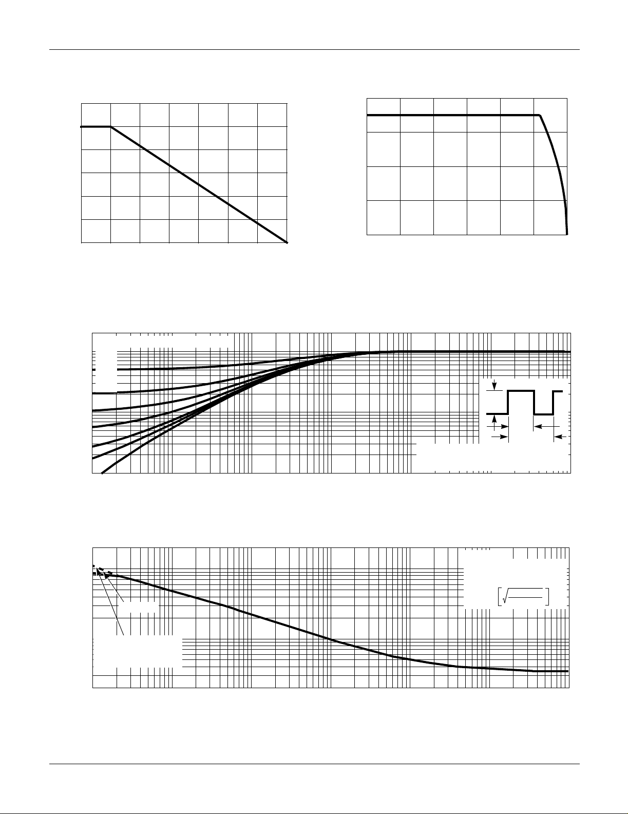
POWER DISSIPATION MULTIPLIER
0
0255075100 175
125
150
TC, CASE TEMPERATURE (oC)
FIGURE 1. NORMALIZED POWER DISSIPATION vs CASE
TEMPERATURE
2
DUTY CYCLE - DESCENDING ORDER
0.5
1
0.2
0.1
0.05
0.02
0.01
0.1
, NORMALIZED
θJC
Z
THERMAL IMPEDANCE
0.01
-5
10
-4
10
-3
10
t, RECTANGULAR PULSE DURATION (s)
40
30
20
, DRAIN CURRENT (A)
10
D
I
0
25 50 75 100 125 150 175
TC, CASE TEMPERATURE (oC)
FIGURE 2. MAXIMUM CONTINUOUS DRAIN CURRENT vs
CASE TEMPERATURE
P
DM
t
NOTES:
DUTY FACTOR: D = t
PEAK TJ = PDM x Z
-2
10
-1
10
θJC
10
1/t2
x R
0
θJC
+ T
1
t
2
C
1
10
FIGURE 3. NORMALIZED MAXIMUM TRANSIENT THERMAL IMPEDANCE
2000
1000
VGS = 10V
100
TRANSCONDUCTANCE
, PEAK CURRENT (A)
DM
I
MAY LIMIT CURRENT
IN THIS REGION
10
-5
10
-4
10
-3
10
-2
10
-1
10
t, PULSE WIDTH (s)
TC = 25oC
FOR TEMPERATURES
ABOVE 25
CURRENT AS FOLLOWS:
I = I
o
C DERATE PEAK
150 - T
25
0
10
125
C
10
FIGURE 4. PEAK CURRENT CAPABILITY
©2002 Fairchild Semiconductor Corporation ISL9N2357D3ST Rev. B1
1
 Loading...