

Fairchild Semiconductor IRLS630A Datasheet
Advanced Power MOSFET
IRLS630A
FEATURES
! Logic-Level Gate Drive
! Avalanche Rugged Technology
! Rugged Gate Oxide Technology
! Lower Input Capacitance
! Improved Gate Charge
! Extended Safe Operating Area
! Lower Leakage Current : 10 μA (Max.) @ VDS= 200V
! Lower R
: 0.335Ω (Typ.)
DS(ON)
Absolute Maximum Ratings
Characteristic Value UnitsSymbol
Drain-to-Source Voltage
Continuous Drain Current (T
Continuous Drain Current (T
Drain Current-Pulsed
=25℃)
C
=100℃)
C
①
Gate-to-Source Voltage
Single Pulsed Avalanche Energy
Avalanche Current
Repetitive Avalanche Energy
Peak Diode Recovery dv/dt
②
①
①
③
Total Power Dissipation (TC=25℃)
Linear Derating Factor
Operating Junction and
Storage Temperature Range
Maximum Lead Temp. for Soldering
Purposes, 1/8" from case for 5-seconds
T
V
DSS
I
I
DM
V
E
I
AR
E
dv/dt
P
, T
J
T
D
GS
AS
AR
D
STG
L
BV
DSS
R
DS(on)
ID= 6.5 A
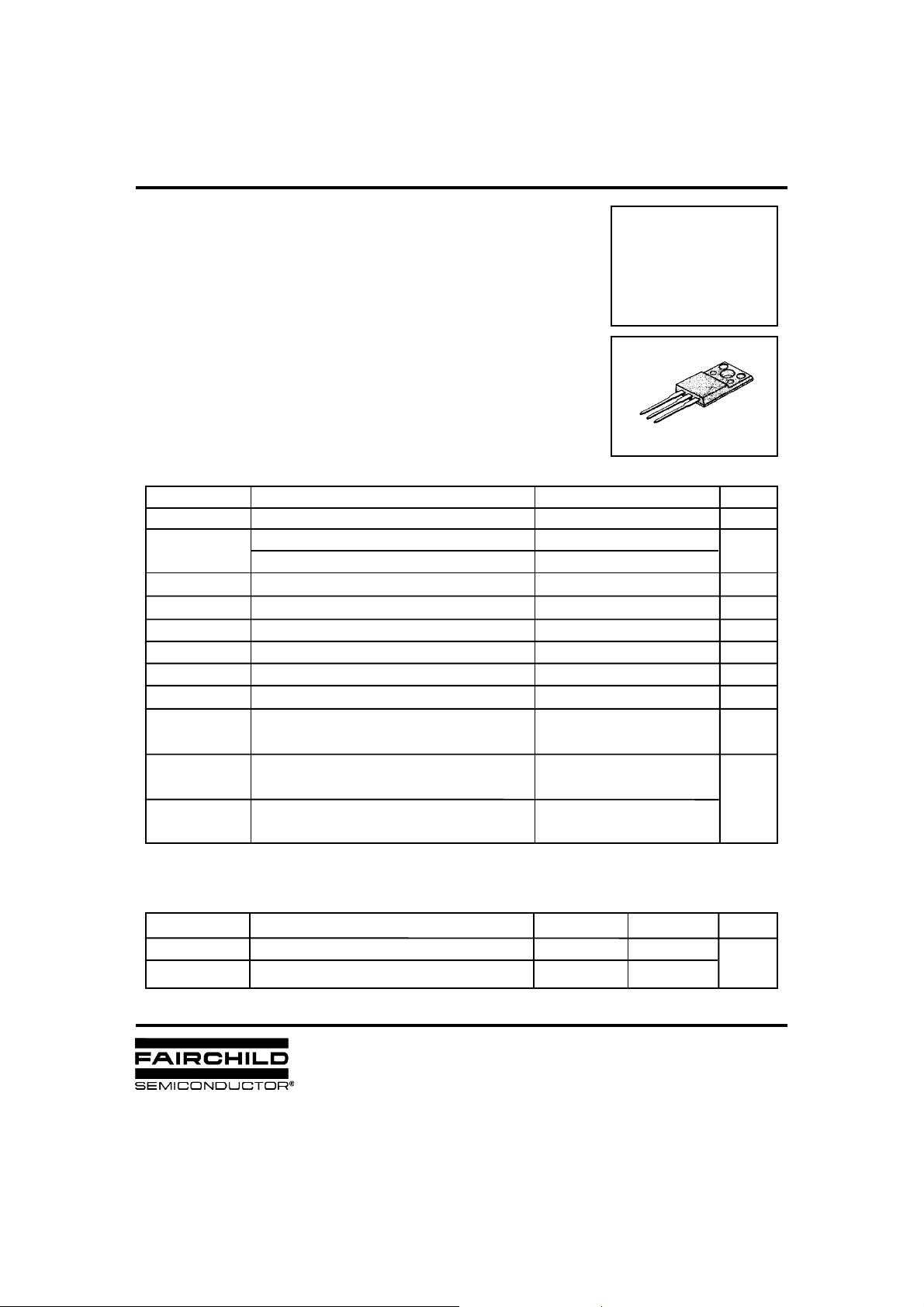
TO-220F
1
2
3
1.Gate 2. Drain 3. Source
200
6.5
4.1
32
±20
56
6.5
3.6
5
36
0.29
- 55 to +150
300
= 200 V
= 0.4 Ω
V
A
A
V
mJ
A
mJ
V/ns
W
W/℃
℃
Thermal Resistance
R
θJC
R
θJA
Characteristic Max. UnitsSymbol Typ.
Junction-to-Case
Junction-to-Ambient
--
--
3.47
62.5
o
C/W
Rev. A
IRLS630A
N-CHANNEL
POWER MOSFET
Electrical Characteristics
CharacteristicSymbol
BV
ΔBV/ΔT
V
GS(th)
I
GSS
I
DSS
R
DS(on)
g
C
C
C
t
d(on)
t
d(off)
Q
Q
Q
Drain-Source Breakdown Voltage
DSS
Breakdown Voltage Temp. Coeff.
J
Gate Threshold Voltage
Gate-Source Leakage , Forward
Gate-Source Leakage , Reverse
Drain-to-Source Leakage Current
Static Drain-Source
On-State Resistance
Forward Transconductance
fs
Input Capacitance
iss
Output Capacitance
oss
Reverse Transfer Capacitance
rss
Turn-On Delay Time
t
Rise Time
r
Turn-Off Delay Time
t
Fall Time
f
Total Gate Charge
g
Gate-Source Charge
gs
Gate-Drain("Miller") Charge
gd
(TC=25℃unless otherwise specified)
Max. UnitsTyp.Min. Test Condition
V
200
--
1.0
--
--
--
--
--
--
--
--
--
--
--
--
--
--
--
--
--
0.18
--
--
--
--
--
--
4.5
580
90
44
8
6
30
9
18.6
3.5
8.3
--
--
2.0
100
-100
10
100
0.4
-755
115
55
25
20
70
30
27
--
--
V
V/℃
V
nA
μA
Ω
S
pF
ns
nC
=0V,ID=250μA
GS
I
=250μA See Fig 7
D
V
DS=VGS
V
=20V
GS
V
=-20V
GS
VDS=200V
V
=160V,TC=125℃
DS
=5V,ID=3.25A
V
GS
VDS=40V,ID=3.25A
VGS=0V,VDS=25V,f =1MHz
VDD=100V,ID=9A,
R
=6Ω
G
VDS=160V,VGS=5V,
I
=9A
D
See Fig 6 & Fig 12
, ID=250μA
See Fig 5
See Fig 13
④
④
④⑤
④⑤
Source-Drain Diode Ratings and Characteristics
CharacteristicSymbol Max. UnitsTyp.Min. Test Condition
I
I
SM
V
t
Q
Notes ;
① Repetitive Rating : Pulse Wi dth Lim i ted by Maximum Junction Temperature
② L=2mH, I
③ I
④ Pulse Test : Pulse Width = 250μs, Duty Cycl e ≤ 2%
⑤ Essentially Independent of Operating Temperature
Continuous Source Current
S
Pulsed-Source Current ①
Diode Forward Voltage
SD
Reverse Recovery Time
rr
Reverse Recovery Charge
rr
=6.5A, VDD=50V, RG=27Ω, Starting TJ =25℃
AS
≤9A, di/dt≤220A/μs, VDD≤BV
SD
④
, Starting TJ =25℃
DSS
--
--
--
--
-158
--
0.78
--
32
1.5
--
--
A
V
ns
μC
9
--
Integral reverse pn-diode
in the MOSFET
T
=25℃,IS=6.5A,VGS=0V
J
T
=25℃,IF=9A
J
di
/dt=100A/μs
F
④
N-CHANNEL
POWER MOSFET
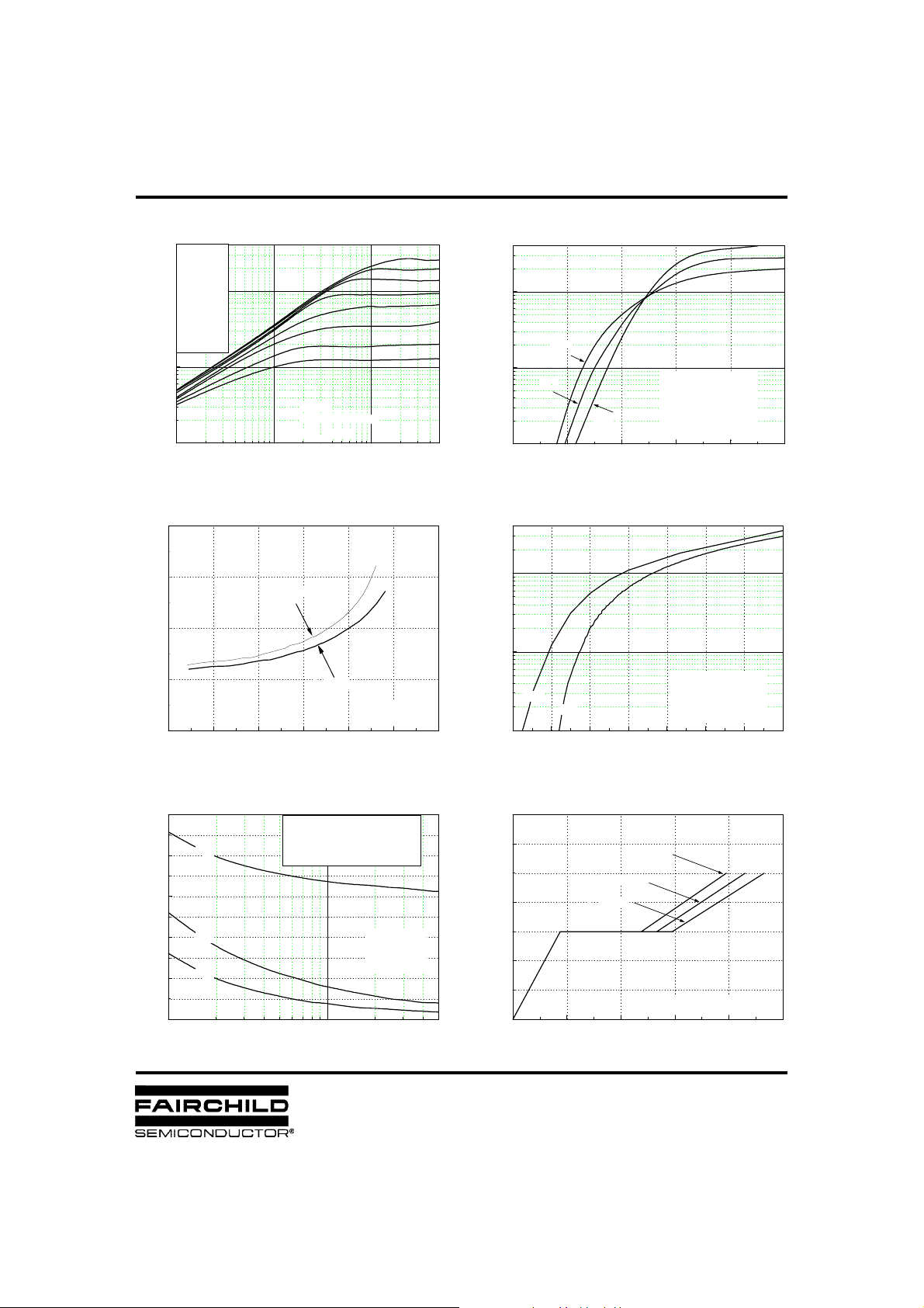
Fig 1. Output Characteristics Fig 2. Transfer Characteristics
V
GS
To p : 7.0 V
6 .0 V
1
5 .5 V
10
5 .0 V
4 .5 V
4 .0 V
3 .5 V
Bo ttom : 3 .0 V
0
10
, Drain Current [A]
D
I
-1
10
-1
10
VDS , Drain-Source Voltag e [V]
@ Notes :
1. 250 µs Pulse Test
2. TC = 25 oC
0
10
IRLS630A
1
10
150 oC
0
10
25 oC
, Drain Curren t [A]
D
I
-1
1
10
10
0246810
- 55 oC
VGS , Gate-Source Voltage [V]
@ Notes :
1. V
2. V
3. 250
= 0 V
GS
= 40 V
DS
s Pulse Test
µ
1.00
0.75
]
Ω
, [
DS(on)
R
0.50
0.25
VGS = 5 V
VGS = 10 V
Drain-Source On-Resistance
0.00
0 5 10 15 20 25 30
900
C
720
ID , Drain Current [A ]
iss
C
= Cgs+ Cgd ( Cds= shorted )
iss
= Cds+ C
C
oss
gd
C
= C
rss
gd
540
C
360
oss
Capacitance [pF]
C
180
rss
0
0
10
1
10
VDS , Drain-Source Voltage [V]
@ No t e : T
@ No t e : T
@ No t e : T@ No t e : T
@ Notes :
1. V
2. f = 1 MHz
= 25 oC
J
= 0 V
GS
Fig 4. Source-Drain Diode Forward VoltageFig 3. On-Resistance vs. Drain Current
1
10
0
10
, Reverse Drain C urrent [A]
150 oC
DR
I
-1
10
0.4 0.6 0.8 1.0 1.2 1.4 1.6 1.8
25 oC
@ Notes :
1. V
2. 250
= 0 V
GS
s Pulse Test
µ
VSD , Source-Drain Voltage [V]
Fig 6. Gate Charge vs. Gate-Source VoltageFig 5. Capacitance vs. Drain-Source Voltage
6
4
2
, Gate-Source Vo ltage [V]
GS
V
0
0 4 8 12 16 20
QG , Total Gate Char ge [nC]
VDS = 40 V
VDS = 100 V
VDS = 160 V
@ Notes : ID = 9 A
 Loading...