

Fairchild Semiconductor IRLW530A, IRLI530A Datasheet
$GYDQFHG 3RZHU 026)(7
IRLW/I530A
FEATURES
Avalanche Rugged Technology
♦
Rugged Gate Oxide Technology
♦
Lower Input Capacitance
♦
Improved Gate Charge
♦
Extended Safe Operating Area
♦
175°C Operating Temperature
♦
Lower Leakage Current: 10µA (Max.) @ V
♦
Lower R
♦
: 0. 101Ω (Typ.)
DS(ON)
Absolute Maximum Ratings
Characteristic Value UnitsSymbol
Drain-to-Source Voltage
Continuous Drain Current (T
Continuous Drain Current (T
Drain Current-Pulsed
Gate-to-Source Volta ge
Single Pulsed Avalanche Energy
Avalanche Current
Repetitive Avalanche Energy
Peak Diode Recovery dv/dt
Total Power Dissipation (TA=25°C)
Total Power Dissipation (T
Linear Derating Factor
Operating Juncti on and
Storage Temperature Range
Maximum Lead Temp. for Soldering
Purposes, 1/8
from case for 5-seconds
T
V
DSS
I
D
I
DM
V
E
I
AR
E
dv/dt
P
, T
J
T
GS
AS
AR
D
STG
L
DS
=25°C)
C
=100°C)
C
=25°C)
C
= 100V
*
(3)
(1)
(2)
(1)
(1)
BV
DSS
R
DS(on)
ID = 14 A
D2-PAK
1
3
1. Gate 2. Drain 3. Source
100
14
9.9
49
20
±
261
14
6.2
6.5
3.8
62
0.41
- 55 to +175
300
= 100 V
= 0.12Ω
I2-PAK
2
1
2
3
V/ns
W/°C
V
A
A
V
mJ
A
mJ
W
W
°C
Thermal Resistance
Characteristic Max. UnitsSymbol Typ.
R
JC
θ
R
θJA
R
θJA
When mounted on the minimum pad size recommended (PCB Mount).
*
©1999 Fairchild Semiconductor Corpor ation
Junction-to-Case
Junction-to-Ambient
Junction-to-Ambient
*
--
--
--
2.41
40
62.5
°C/W
Rev. B
1
IRLW/I530A
1&+$11(/
32:(5 026)(7
Electrical Characteristics
CharacteristicSymbol
BV
∆BV/∆T
V
R
DSS
GS(th)
I
GSS
I
DSS
DS(on)
g
fs
C
iss
C
oss
C
rss
t
d(on)
t
r
t
d(off)
t
f
Q
Q
gs
Q
gd
Drain-Source Breakdown Voltage
Breakdown Voltage Temp. Coeff.
J
Gate Threshold Voltage
Gate-Source Leakage , Forwar d
Gate-Source Leakage , Revers e
Drain-to-Sou rce Leakage Current
Static Drain-Source
On-State Resistance
Forward Transconductance
Input Capacitance
Output Capacitance
Reverse Transfer Capacitance
Turn-On Delay Time
Rise Time
Turn-Off Delay Time
Fall Time
Total Gate Charge
g
Gate-Source Charge
Gate-Drain (
Miller ) Charge
(TC=25°C unless otherwise specified)
Max. UnitsTyp.Min. Test Condition
V
100
--
1.0
--
--
--
--
--
--
--
--
--
--
--
--
--
--
--
--
--
0.1
--
--
--
--
--
--
10.2
580
140
60
10
11
29
15
16.9
2.7
9.7
--
--
2.0
100
-100
10
100
0.12
-755
175
75
30
30
70
40
24
--
--
V
V/°C
V
nA
A
µ
Ω
pF
ns
nC
=0V,ID=250µA
GS
I
=250µA
D
VDS=5V,ID=250µA
=20V
V
GS
V
=-20V
GS
V
=100V
DS
V
=80V,TC=150°C
DS
=5V,ID=7A
V
GS
Ω
VDS=40V,ID=7A
V
=0V,VDS=25V,f =1MHz
GS
See Fig 5
VDD=50V,ID=14A,
R
=6
G
VDS=80V,VGS=5V,
=14A
I
D
See Fig 6 & Fig 12
See Fig 7
Ω
See Fig 13
(4)
(4)
(4) (5)
(4) (5)
Source-Drain Diode Ratings and Characteristics
CharacteristicSymbol Max. UnitsTyp.Min. Test Condition
I
I
SM
V
t
Q
Notes;
(1) Repetitive Rating: Pu lse Width Limite d by Maximum Junction Temperature
(2) L=2mH, I
(3) I
(4) Pulse Test: Puls e Width = 250µs, Duty Cycle ≤ 2%
(5) Essentially Independent of Operating Temperature
Continuous Source Current
S
Pulsed- S o u rce Curre nt
Diode Forward Voltage
SD
Reverse Recove ry T ime
rr
Reverse Recovery Ch arge
rr
=14A, VDD=25V, RG=27Ω, Starting TJ =25°C
AS
14A, di/dt ≤ 350A/µs, V
≤
SD
DD
≤
BV
DSS
--
(1)
--
(4)
--
--
--
, Starting TJ =25°C
--
--
--
109
0.41
14
49
1.5
--
--
ns
µ
A
V
C
Integral reverse pn-diode
in the MOSFET
T
=25°C,IS=14A,VGS=0V
J
T
=25°C,IF=14A
J
di
/dt=100A/µs
F
(4)
2
1&+$11(/
32:(5 026)(7
IRLW/I530A
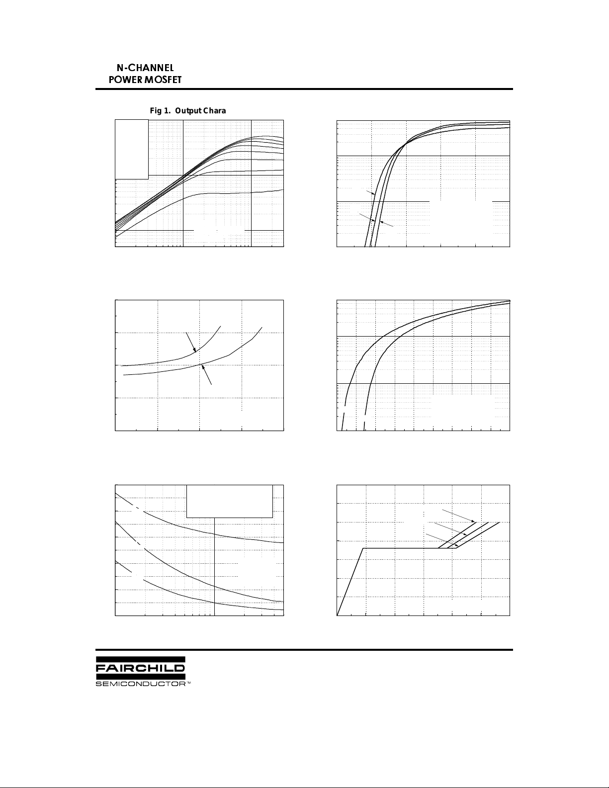
Fig 1. Output Characteristics Fig 2. Transfer Characteristics
GS
@ Note s :
1. 2 50 µs Puls e Test
2. TC = 25 oC
0
10
1
10
, Drain Current [A]
I
10
10
D
10
2
V
Top : 7.0 V
6 .0 V
5 .5 V
5 .0 V
4 .5 V
4 .0 V
3 .5 V
1
Bo ttom : 3 .0 V
0
-1
10
VDS , Drain-Source Voltage [V]
0.20
VGS = 5 V
VGS = 10 V
]
Ω
, [
DS(on)
R
0.15
0.10
0.05
Drain-Source On-Resistance
@ Note : TJ = 25 oC
0.00
0 15304560
ID , Drain Current [A]
1
10
175 oC
0
10
, Drain C urrent [A]
I
D
25 oC
- 55 oC
-1
10
0246810
@ Notes :
1. V
GS
2. V
DS
3. 250
= 0 V
= 40 V
s Pulse Test
µ
VGS , Gate-So urce Voltage [V]
Fig 4. Source-Drain Diode Forward VoltageFig 3. On-Resistance vs. Drain Current
1
10
0
10
, Reverse Drain Current [A]
175 oC
DR
I
10
25 oC
-1
0.4 0.6 0.8 1.0 1.2 1.4 1.6 1.8 2.0 2.2
@ Notes :
1. V
GS
2. 250
= 0 V
s Pulse Test
µ
VSD , Source- Drain Voltage [V]
1000
C
iss
800
600
C
oss
400
Capacitance [pF]
C
rss
200
0
0
10
VDS , Drain-Source Voltage [V]
C
= Cgs+ Cgd ( Cds= shorted )
iss
C
= Cds+ C
oss
gd
C
= C
rss
gd
1
10
@ Notes :
1. V
= 0 V
GS
2. f = 1 MHz
6
VDS = 20 V
VDS = 50 V
VDS = 80 V
4
2
, Gate-So urce Voltage [V]
GS
V
0
0369121518
@ Notes : ID = 14 A
QG , Total G ate Charge [nC]
Fig 6. Gate Charge vs. Gate-Source VoltageFig 5. Capacitan ce vs. Drain-Source Voltage
 Loading...