

Fairchild Semiconductor IRLI520A Datasheet
IRLW/I520A
BV
DSS
= 100 V
R
DS(on)
= 0.22 Ω
ID= 9.2 A
100
9.2
6.5
32
±20
112
9.2
4.9
6.5
3.8
49
0.33
- 55 to +175
300
3.04
40
62.5
--
--
--
1
■ Avalanche Rugged Technology
■ Rugged Gate Oxide Technology
■ Lower Input Capacitance
■ Improved Gate Charge
■ Extended Safe Operating Area
■ 175℃ Operating Temperature
■ Lower Leakage Current : 10 μA (Max.) @ VDS= 100V
■ Lower R
DS(ON)
: 0.176 Ω (Typ.)
Advanced Power MOSFET
Thermal Resistance
Junction-to-Case
Junction-to-Ambient
Junction-to-Ambient
R
θJC
R
θJA
R
θJA
℃/W
Characteristic Max. UnitsSymbol Typ.
FEATURES
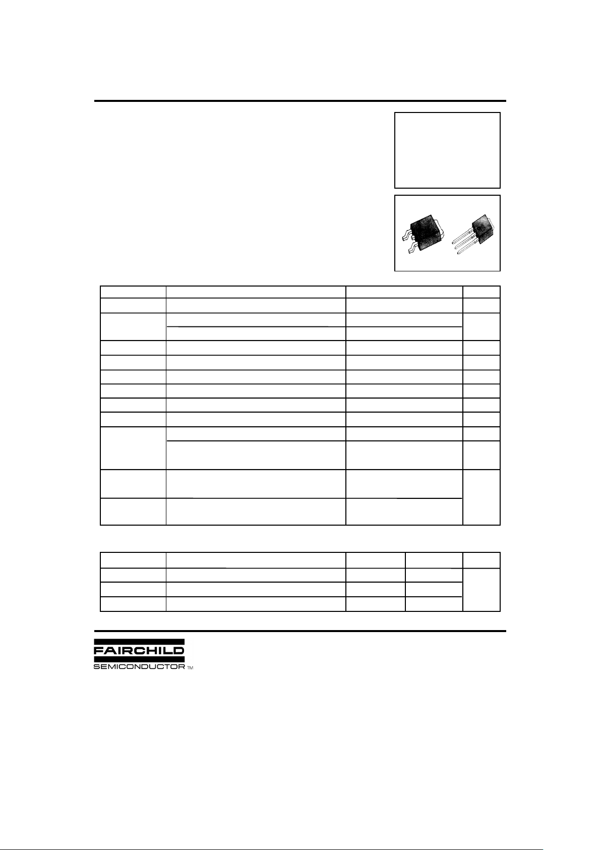
D2-PAK
1. Gate 2. Drain 3. Source
1
3
2
1
2
3
I2-PAK
*
*
When mounted on the mi nimum pad size recommended (PCB Mount).
Absolute Maximum Ratings
Drain-to-Source Voltage
Continuous Drain Current (T
C
=25℃)
Continuous Drain Current (T
C
=100℃)
Drain Current-Pulsed
①
Gate-to-Source Voltage
Single Pulsed Avalanche Energy ②
Avalanche Current
①
Repetitive Avalanche Energy
①
Peak Diode Recovery dv/dt
③
Total Power Dissipation (TA=25℃)
Total Power Dissipation (T
C
=25℃)
Linear Derating Factor
Operating Junction and
Storage Temperature Range
Maximum Lead Temp. for Soldering
Purposes, 1/8” from case for 5-seconds
Characteristic Value UnitsSymbol
I
DM
V
GS
E
AS
I
AR
E
AR
dv/dt
P
D
I
D
T
J
, T
STG
T
L
A
V
mJ
A
mJ
V/ns
W
W
W/℃
A
℃
V
DSS
V
*
IRLW/I520A
100
--
1.0
--
--
--
--
--
0.1
--
--
--
--
--
90
39
5
10
19
9
10.2
1.7
6.0
--
--
2.0
100
-100
10
100
0.22
-440
115
50
20
30
50
30
15
--
--
7.7
340
--
--
--
98
0.34
9.2
32
1.5
--
--
Notes ;
① Repetitive Rating : Pulse Wi dth Lim i ted by Maximum Junction Temperature
② L=2mH, I
AS
=9.2A, VDD=25V, RG=27Ω, Starting TJ =25℃
③ I
SD
≤9.2A, di/dt≤300A/μs, VDD≤BV
DSS
, Starting TJ =25℃
④ Pulse Test : Pulse Width = 250μs, Duty Cycl e ≤ 2%
⑤ Essentially Independent of Operating Temperature
2
N-CHANNEL
POWER MOSFET
Electrical Characteristics
(TC=25℃ unless otherwise specified)
Drain-Source Breakdown Voltage
Breakdown Voltage Temp. Coeff.
Gate Threshold Voltage
Gate-Source Leakage , Forward
Gate-Source Leakage , Reverse
CharacteristicSymbol
Max. UnitsTyp.Min. Test Condition
Static Drain-Source
On-State Resistance
Forward Transconductance
Input Capacitance
Output Capacitance
Reverse Transfer Capacitance
Turn-On Delay Time
Rise Time
Turn-Off Delay Time
Fall Time
Total Gate Charge
Gate-Source Charge
Gate-Drain("Miller") Charge
g
fs
C
iss
C
oss
C
rss
t
d(on)
t
r
t
d(off)
t
f
Q
g
Q
gs
Q
gd
BV
DSS
Δ
BV/ΔT
J
V
GS(th)
R
DS(on)
I
GSS
I
DSS
V
V/℃
V
nA
μA
Ω
Ω
pF
ns
nC
--
--
--
--
--
--
--
--
--
--
--
--
--
V
GS
=0V,ID=250μA
I
D
=250μA See Fig 7
V
DS
=5V,ID=250μA
V
GS
=20V
V
GS
=-20V
VDS=100V
V
DS
=80V,TC=150℃
V
GS
=5V,ID=4.6A
④
VDS=40V,ID=4.6A
④
VDD=50V,ID=9.2A,
R
G
=9
Ω
See Fig 13
④⑤
VDS=80V,VGS=5V,
I
D
=9.2A
See Fig 6 & Fig 12
④⑤
Drain-to-Source Leakage Current
VGS=0V,VDS=25V,f =1MHz
See Fig 5
Source-Drain Diode Ratings and Characteristics
Continuous Source Current
Pulsed-Source Current
①
Diode Forward Voltage
④
Reverse Recovery Time
Reverse Recovery Charge
I
S
I
SM
V
SD
t
rr
Q
rr
CharacteristicSymbol Max. UnitsTyp.Min. Test Condition
--
--
--
--
--
A
V
ns
μC
Integral reverse pn-diode
in the MOSFET
T
J
=25℃,IS=9.2A,VGS=0V
T
J
=25℃,IF=9.2A
di
F
/dt=100A/μs
④
IRLW/I520A
10
-1
10
0
10
1
10
-1
10
0
10
1
@ Notes :
1. 250 µs Pulse Test
2. TC = 25 oC
V
GS
Top : 7 .0 V
6 .0 V
5 .5 V
5 .0 V
4 .5 V
4 .0 V
3 .5 V
Bo tto m : 3 .0 V
I
D
, Drain Current [A ]
VDS , Drain-Source Voltage [V]
0246810
10
-1
10
0
10
1
25 oC
175 oC
- 55 oC
@ Notes :
1. V
GS
= 0 V
2. V
DS
= 40 V
3. 250
µ
s Pulse Test
I
D
, Drain Current [A ]
VGS , Gate-Source Vo ltage [V]
0 10203040
0.0
0.1
0.2
0.3
0.4
@ Note : TJ = 25 oC
VGS = 10 V
VGS = 5 V
R
DS(on)
, [
Ω
]
Drain-Source On-Resistance
ID , Drain Current [A ]
024681012
0
2
4
6
VDS = 80 V
VDS = 50 V
VDS = 20 V
@ Notes : ID = 9.2 A
V
GS
, Gate-Source Vo ltage [V]
QG , Total Gate Char ge [nC]
0.4 0.6 0.8 1.0 1.2 1.4 1.6 1.8 2.0 2.2
10
-1
10
0
10
1
175 oC
25 oC
@ Notes :
1. V
GS
= 0 V
2. 250
µ
s Pulse Test
I
DR
, Reverse Drain C urrent [A]
VSD , Source-Drain Voltage [V]
10
0
10
1
0
120
240
360
480
600
C
iss
= Cgs+ Cgd ( Cds= shorted )
C
oss
= Cds+ C
gd
C
rss
= C
gd
@ Notes :
1. V
GS
= 0 V
2. f = 1 MHz
C
rss
C
oss
C
iss
Capacitance [pF]
VDS , Drain-Source Voltage [V]
3
N-CHANNEL
POWER MOSFET
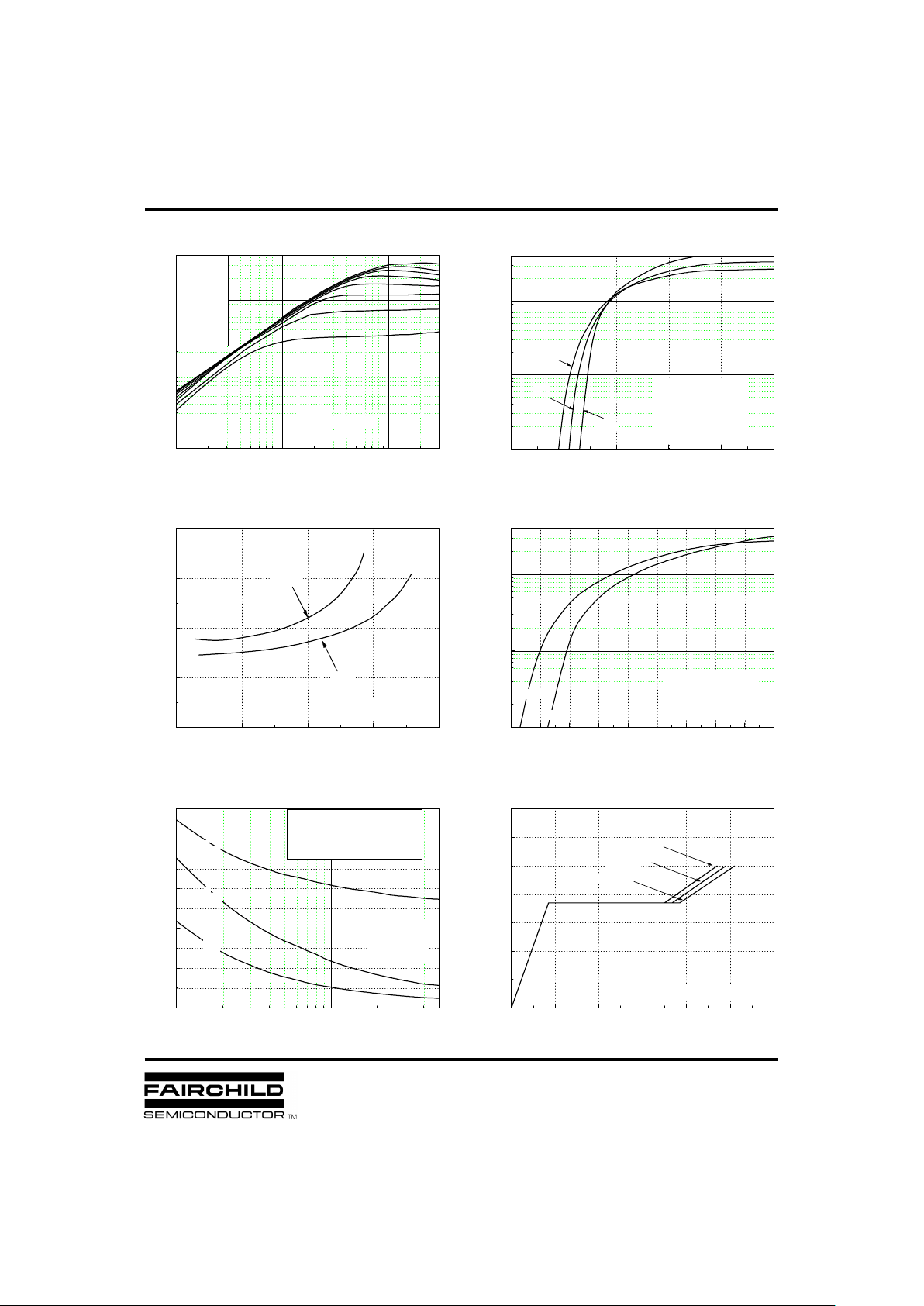
Fig 1. Output Characteristics Fig 2. Transfer Characteristics
Fig 6. Gate Charge vs. Gate-Source VoltageFig 5. Capacitance vs. Drain-Source Voltage
Fig 4. Source-Drain Diode Forward VoltageFig 3. On-Resistance vs. Drain Current
 Loading...