

Fairchild Semiconductor IRF634A Datasheet
$GYDQF HG 3RZH U 026)(7
IRF634A
FEATURES
Avalanche Rugged Technology
♦
Rugged Gate Oxide Technology
♦
Lower Input Capacitance
♦
Improved Gate Charge
♦
Extended Safe Operating Area
♦
Lower Leakage Current: 10µA (Max.) @ V
♦
Lower R
♦
: 0.327Ω (Typ.)
DS(ON)
Absolute Maximum Ratings
Characteristic Value UnitsSymbol
Drain-to-Source Voltage
Continuous Drain Current (T
Continuous Drain Current (T
Drain Current-Pulsed
Gate-to-Source Volta ge
Single Pulsed Avalanche Energy
Avalanche Current
Repetitive Avalanche Energy
Peak Diode Recovery dv/dt
Total Power Dissipation (TC=25°C)
Linear Derating Factor
Operating Juncti on and
Storage Temperature Range
Maximum Lead Temp. for Soldering
Purposes, 1/8
from case for 5-seconds
T
V
DSS
I
D
I
DM
V
E
I
AR
E
dv/dt
P
, T
J
T
GS
AS
AR
D
STG
L
= 250V
DS
=25°C)
C
=100°C)
C
(1)
(2)
(1)
(1)
(3)
BV
R
DSS
DS(on)
= 250 V
ID = 8.1 A
TO-220
1
2
3
1.Gate 2. Drain 3. Source
250
8.1
5.1
32
30
±
205
8.1
7.4
4.8
74
0.59
- 55 to +150
300
= 0.45Ω
V
A
A
V
mJ
A
mJ
V/ns
W
W/°C
°C
Thermal Resistance
R
JC
θ
R
θCS
R
θJA
©1999 Fairchild Semiconductor Corpor ation
Characteristic Max. UnitsSymbol Typ.
Junction-to-Case
Case-to-Sink
Junction-to-Ambient
--
0.5
--
1.69
--
62.5
°C/W
Rev. B
IRF634A
1&+$1 1(/
32:(5 026)(7
Electrical Characteristics
CharacteristicSymbol
BV
∆BV/∆T
V
I
I
R
C
C
t
t
DSS
GS(th)
GSS
DSS
DS(on)
g
fs
C
iss
oss
rss
d(on)
t
r
d(off)
t
f
Q
g
Q
gs
Q
gd
Drain-Source Breakdown Voltage
Breakdown Voltage Temp. Coeff.
J
Gate Threshold Voltage
Gate-Source Leakage , Forwar d
Gate-Source Leakage , Revers e
Drain-to-Sou rce Leakage Current
Static Drain-Source
On-State Resistance
Forward Transconductance
Input Capacitance
Output Capacitance
Reverse Transfer Capacitance
Turn-On Delay Time
Rise Time
Turn-Off Delay Time
Fall Time
Total Gate Charge
Gate-Source Charge
Gate-Drain (
Miller ) Charge
(TC=25°C unless otherwise specified)
Max. UnitsTyp.Min. Test Condition
V
250
--
2.0
--
--
--
--
--
--
--
--
--
--
--
--
--
--
--
--
--
0.29
--
--
--
--
--
--
6.1
730
110
50
13
14
53
21
30
5.8
13.5
--
--
4.0
100
-100
10
100
0.45
-950
130
60
40
40
120
50
40
--
--
V
V/°C
V
nA
A
µ
Ω
pF
ns
nC
=0V,ID=250µA
GS
I
=250µA
D
VDS=5V,ID=250µA
=30V
V
GS
=-30V
V
GS
V
=250V
DS
V
=200V,TC=125°C
DS
=10V,ID=4.05A
V
GS
Ω
VDS=40V,ID=4.05A
V
=0V,VDS=25V,f =1MHz
GS
See Fig 5
VDD=125V,ID=8.1A,
=12
R
G
VDS=200V,VGS=10V,
=8.1A
I
D
See Fig 6 & Fig 12
See Fig 7
Ω
See Fig 13
(4)
(4)
(4) (5)
(4) (5)
Source-Drain Diode Ratings and Characteristics
CharacteristicSymbol Max. UnitsTyp.Min. Test Condition
I
I
SM
V
t
Q
Notes;
(1) Repetitive Rating: Pu lse Width Limited by Maximum Junction Temperatu re
(2) L=5mH, I
(3) I
(4) Pulse Test: Pulse Width = 250µs, Duty Cycle ≤ 2%
(5) Essentially Independent of Operating Temper ature
Continuous Source Current
S
Pulsed- S o u rce Curren t
Diode Forward Voltage
SD
Reverse Recove ry T ime
rr
Reverse Recovery Ch arge
rr
=8.1A, VDD=50V, RG=27Ω, Starting TJ =25°C
AS
8.1A, di/dt ≤ 210A/µs, V
≤
SD
DD
≤
BV
DSS
--
(1)
--
(4)
--
--
--
, Starting TJ =25°C
--
--
--
190
1.28
8.1
32
1.5
--
--
µ
A
V
ns
C
Integral reverse pn-diode
in the MOSFET
T
=25°C,IS=8.1A,VGS=0V
J
T
=25°C,IF=8.1A
J
/dt=100A/µs
di
F
(4)
µ
1&+$11(/
32:(5 026)(7
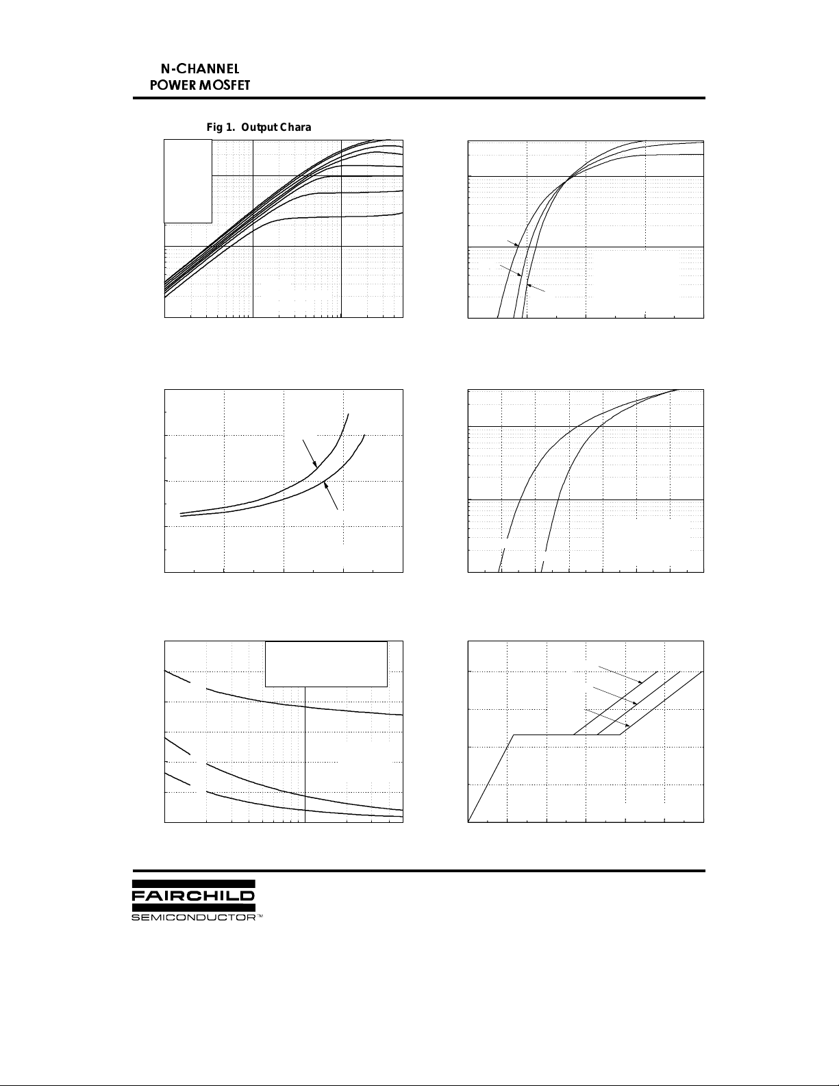
Fig 1. Output Characteristics Fig 2. Transfer Characteristics
V
GS
Top : 1 5 V
1 0 V
1
8.0 V
10
7 .0 V
6.0 V
5 .5 V
5 .0 V
Bott om : 4.5 V
IRF634A
1
10
0
10
, Drain C urrent [A]
D
I
-1
10
-1
10
@ Notes :
1. 250 µs Pulse Test
2. TC = 25 oC
0
10
1
10
VDS , Drain-S ource Voltage [V]
1.00
VGS = 10 V
VGS = 20 V
]
Ω
, [
DS(on)
R
0.75
0.50
0.25
Drain-Source On-Resis tance
@ Note : TJ = 25 oC
0.00
010203040
ID , Drain Current [A]
1200
800
C
iss
C
= Cgs+ Cgd ( Cds= shorted )
iss
= Cds+ C
C
oss
gd
C
= C
rss
gd
150 oC
0
10
25 oC
, Drai n Current [A]
D
I
-1
10
246810
- 55 oC
@ Notes :
1. V
2. V
3. 250
= 0 V
GS
= 40 V
DS
s Pulse Test
µ
VGS , Gate -Source Voltag e [V]
Fig 4. Source-Drain Diode Forward VoltageFig 3. On-Resistance vs. Drain Curr ent
1
10
0
10
, Reverse Dra in Current [A]
I
DR
10
150 oC
25 oC
-1
0.20.40.60.81.01.21.41.6
@ Notes :
1. V
2. 250
GS
= 0 V
s Pulse Test
VSD , Source-Drai n Voltage [V]
Fig 6. Gate Charge vs. Gate-Source VoltageFig 5. Capacitance vs. Drain-Sour ce Voltage
10
VDS = 50 V
VDS = 125 V
VDS = 200 V
@ Notes :
1. V
= 0 V
GS
2. f = 1 MHz
1
Capacitanc e [pF]
C
400
oss
C
rss
0
0
10
10
VDS , Drain-S ource Voltage [V]
5
, Gate -Source Voltag e [V]
GS
V
0
0 5 10 15 20 25 30
@ Notes : ID = 8.1 A
QG , Tota l Gate Charge [nC]
 Loading...