

Fairchild Semiconductor ILC5062AM28 Datasheet
www.fairchildsemi.com
Rev. 2.2 8/14/02
Features
• All-CMOS design in SOT-23 or SC70 package
• A grade ±1% precision in Reset Detection
• Standard grade : ±2% precision in Reset Detection
• Only 1µA of Iq
• Over 2mA of sink current capability
• Built-in hysteresis of 5% of detection voltage
• Voltage options of 2.6, 2.7, 2.8, 2.9, 3.1, 4.4, and 4.6V fit
most supervisory applications
• Active low push-pull output
Applications
• Microprocessor reset circuits
• Memory battery back-up circuitry
• Power-on reset circuits
• Portable and battery powered electronics
Description
All-CMOS voltage monitoring circuit in either a 3-lead
SOT-23 or SC70 package offers the best performance in
power consumption and accuracy.
The ILC5062 is available in a series of ±1% (A-grade) or 2%
(standard grade) accurate trip voltages to fit most microprocessor applications. Even though its output can sink over
2mA, the device draws only 1µA in normal operation.
Additionally, a built-in hysteresis of 5% of detect voltage
simplifies system design.
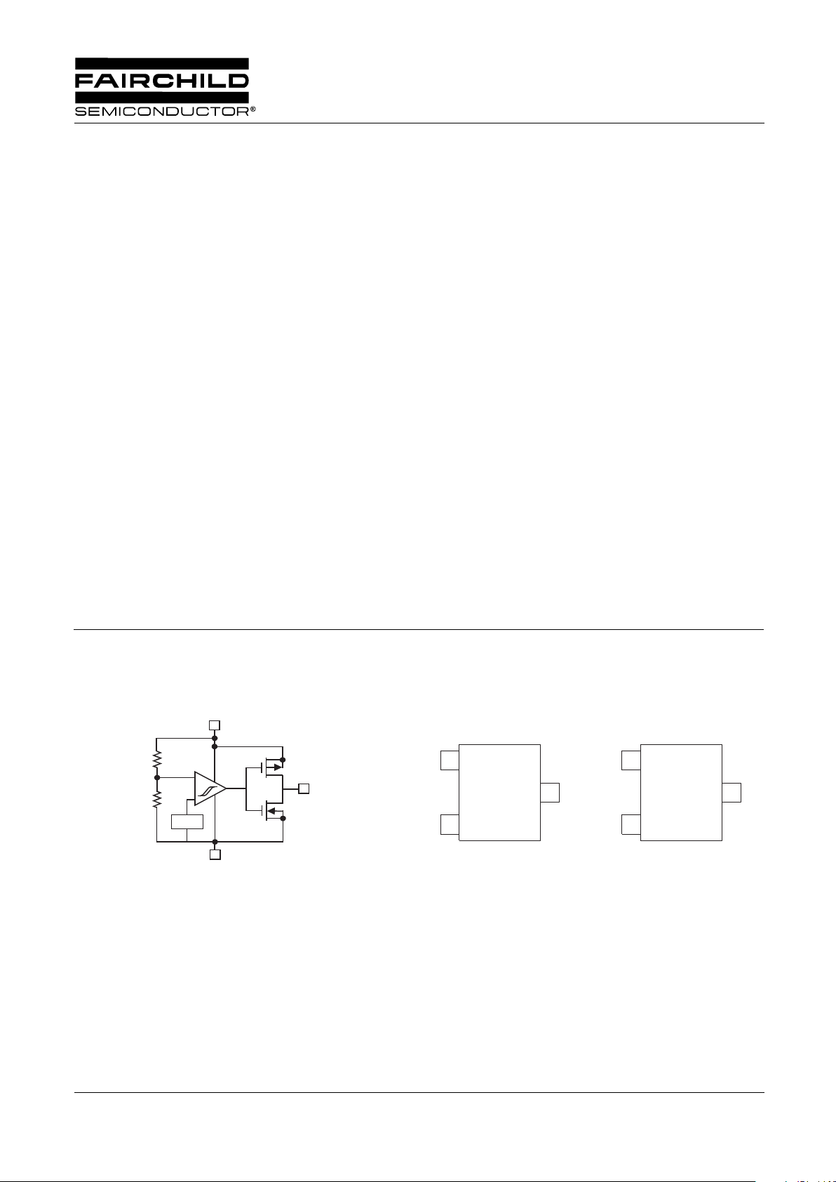
Pin-Package Configurations
Block Diagram
V
REF
V
IN
V
SS
V
OUT
Complementary CMOS Output
V
IN
Top View
V
SS
V
OUT
2
1
3
V
IN
V
SS
V
OUT
2
1
3
SC-70
SOT-23
ILC5062
SOT-23 Power Supply reset Monitor with 1% precision
Rev. 2.2 8/14/02 2
PRODUCT SPECIFICATION ILC5062
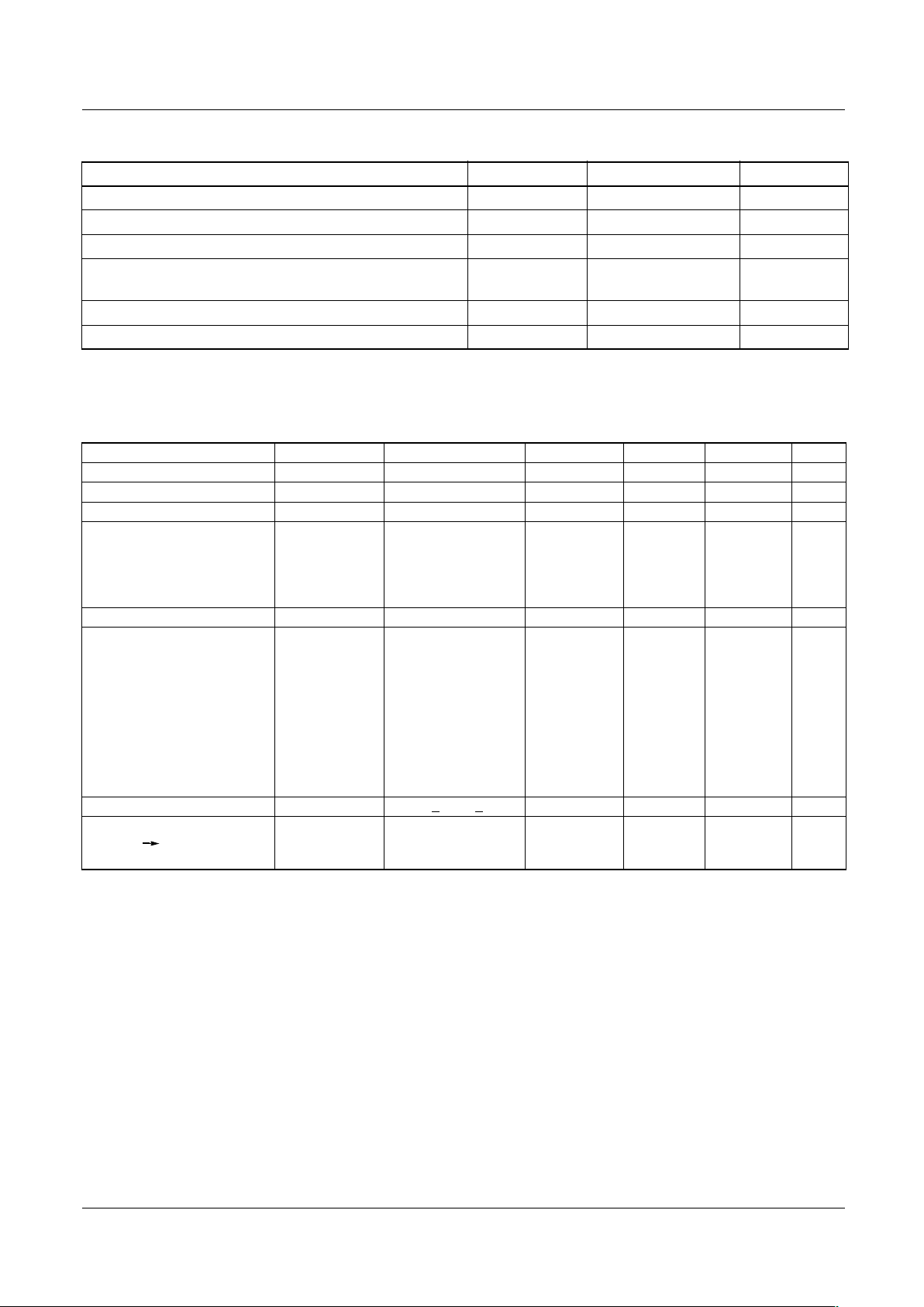
Absolute Maximum Ratings
Electrical Characterisitcs ILC5062
(TA=25°C)
Note1: An additional resistor between the V
IN
pin and supply voltage may cause deterioration of the characteristics due to
increasing of V
DR
.
Note2: Vout=Gnd when 1V< V
IN
<1.5V
Note3: Iout < 10uA when V
IN
<1V
Parameter Symbol Ratings Units
Input Voltage V
IN
12 V
Output Current I
OUT
50 mA
Output Voltage V
OUT
VSS-0.3~VIN=+0.3 V
Continuous Total
Power Dissipation (SOT-23)
P
D
150 mW
Operating Ambient Temperature T
opr
-30~+80 °C
Storage Temperature T
stg
-40~+125 °C
Parameter Symbol Conditions Min. Typ. Max. Units
Detect Fail Voltage V
DF
A grade VDF X 0.99 V
DF
VDF X 1.01 V
Detect Fail Voltage V
DF
Standard grade VDF X 0.98 V
DF
VDF X 1.02 V
Hysteresis Range V
HYS
VDF X 0.02 VDF X 0.05 VDF X 0.08 V
Supply Current
I
SS
VIN = 1.5V
V
IN
= 2.0V
V
IN
= 3.0V
V
IN
= 4.0V
V
IN
= 5.0V
0.9
1.0
1.3
1.6
2.0
2.6
3.0
3.4
3.8
4.2
µA
Operating Voltage V
IN
VDF = 2.1 ~ 6.0V 1.5 10.0 V
Output Current
I
OUT
N-ch VDS = 0.5V
V
IN
= 1.0V
V
IN
= 2.0V
V
IN
= 3.0V
V
IN
= 4.0V
V
IN
= 5.0V
P-Ch VDS = 2.1V
V
IN
= 8V
2.2
7.7
10.1
11.5
13.0
-10
mA
Temperature Characteristics ∆V
DF
/(∆T
opr•VDF
) -30°C < Topr < 80°C -200 ±100 +200 ppm/°C
Delay Time (Release
Voltage Output Inversion)
t
DLY
(VDR to V
OUT
Inversion)
0.1 ms
PRODUCT SPECIFICATION ILC5062
Rev. 2.2 8/14/02 3
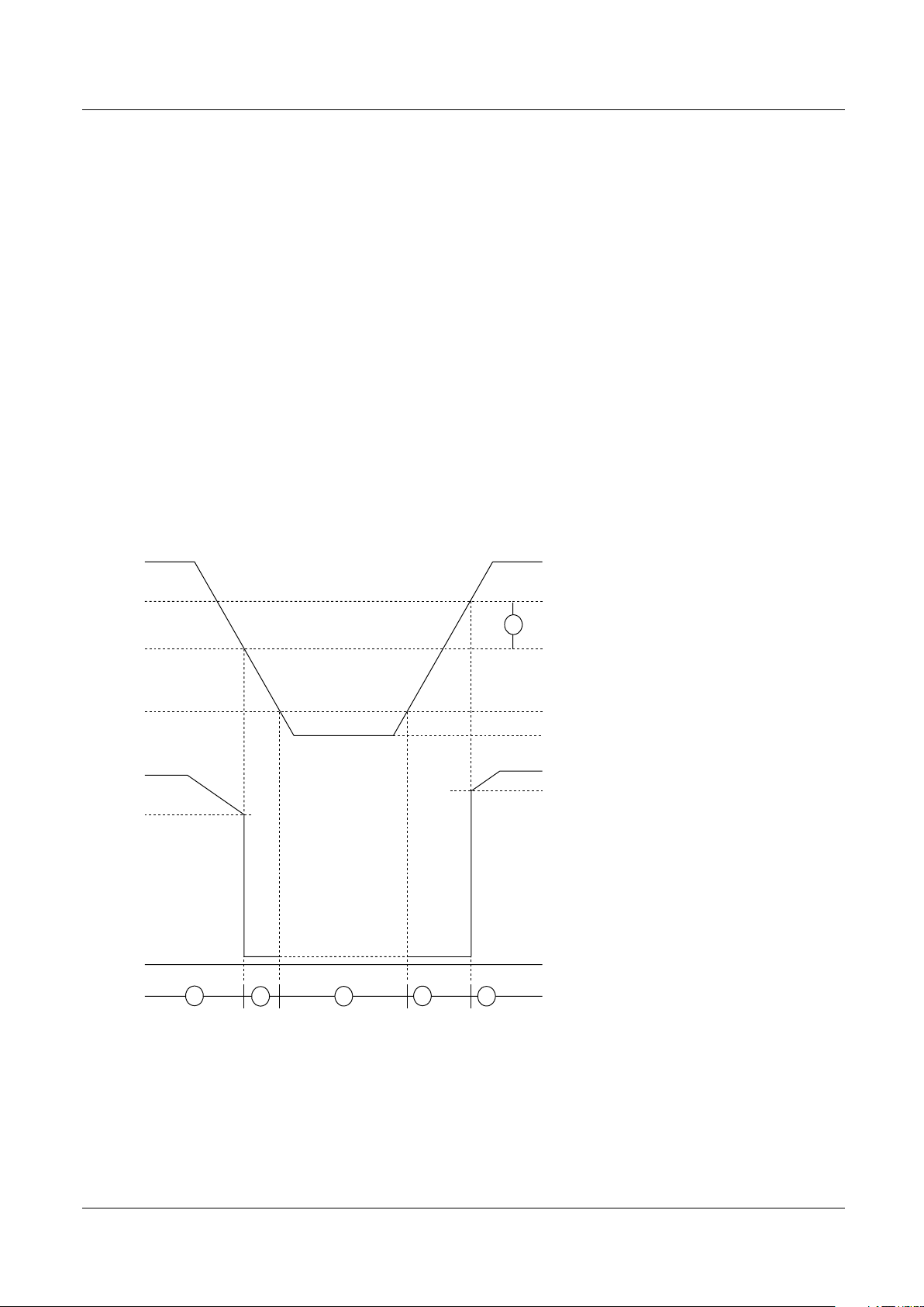
6
5
4
3
1
2
INPUT VOLTAGE (V
IN)
DETECT RELEASE VOLTAGE (V
DR)
DETECT FAIL VOLTAGE (V
DF)
MINIMUM OPERATING VOLTAGE (V
MIN)
GROUND VOLTAGE (V
SS)
OUTPUT VOLTAGE (V
OUT)
GROUND VOLTAGE (V
SS)
Functional Description
The following designators 1~6 refer to the timing diagram below.
1. While the input voltage (V
IN
) is higher than the detect voltage (VDF), the output voltage at V
OUT
pin equals the input volt-
age at V
IN
pin.
2. When the input V
IN
voltage falls lower than VDF, V
OUT
drops near ground voltage.
3. If the input voltage decreases below the minimum operating voltage (V
MIN
), the V
OUT
output voltage will be undefined.
4. During an increase of the input voltage from the V
SS
voltage, V
OUT
is undefined at the voltage below V
MIN
. Exceeding the
V
MIN
level, the ouput stays at the ground level (VSS) between the minimum operating voltage (V
MIN
) and the detect release
voltage (V
DR
).
5. If the input voltage increases more than V
DR
, the output voltage at V
OUT
pin equals the input voltage at VIN pin.
6. The difference between V
DR
and VDF is the hysteresis in the system.
 Loading...