

Fairchild Semiconductor HUF76121D3, HUF76121D3S Datasheet
HUF76121D3, HUF76121D3S
Data Sheet January 2003
20A, 30V, 0.023 Ohm, N-Channel, Logic
Level UltraFET Power MOSFETs
These N-Channel pow er MOSFETs
are manufactured using the
innovati ve UltraFET™ process.
This advanced process technology
achieves the lowest possible on-resistance per silicon ar ea,
resultin g in outstanding performance. This device is capab le
of withstanding hi gh energy in the avalanche mode and the
diode exhibits very low reverse recovery time and stored
charge. It was design ed for use in applicati ons where power
efficiency is important, such as switching regulators,
switchi ng converters, motor drivers, relay drivers , lowvoltage bus switches, and power manage me nt i n po rtab le
and battery-operated products.
Formerly developmental ty pe TA76121.
Ordering Information
PART NUMBER PACKAGE BRAND
HUF76121D3 TO-251AA 76121D
HUF76121D3S TO-252AA 76121D
NOTE: When ordering, use the entire part number. Add the suffix T to
obtain the TO-252AA variant in tape and reel, e.g., HUF76121D3ST.
Features
• Logic Level Gate Drive
• 20A, 30V
• Ultra Low On-Resistance, r
• Temperatur e Compensating PSPICE
• Temperatur e Compensating SABER
DS(ON)
= 0.023Ω
®
Model
©
Model
• Thermal Impedance SPICE Model
• Thermal Impedance SABER Model
• Peak Current vs Pulse Width Curve
• UIS Rating Curve
• Related Literature
- TB334, “Guidelines for Soldering Surface Mount
Components to PC Boards”
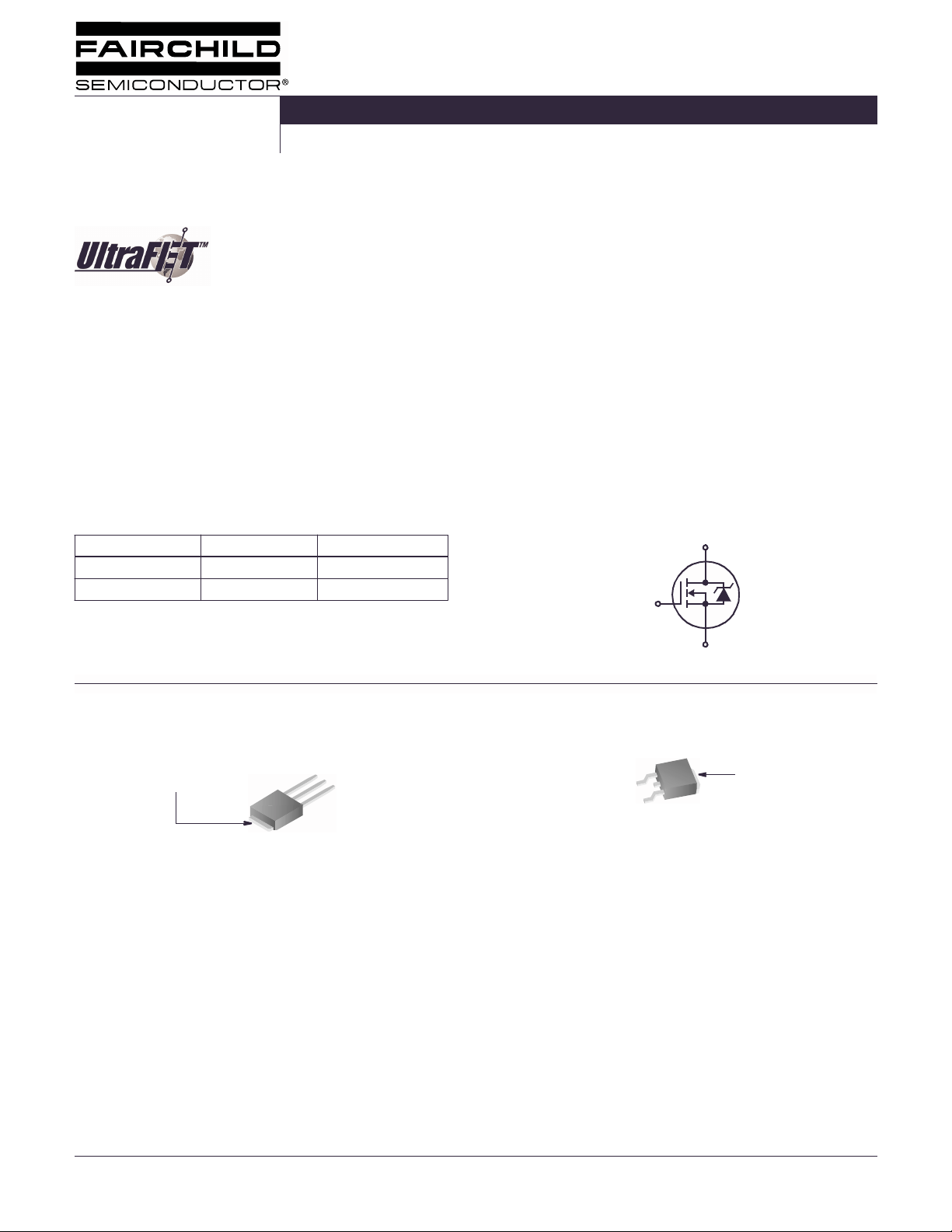
Symbol
D
G
S
Packaging
(FLANGE)
DRAIN
JEDEC TO-251AA JEDEC TO-252AA
SOURCE
DRAIN
GATE
GATE
SOURCE
DRAIN
(FLANGE)
©2003 Fairchild Semiconductor Corporation HUF76121D3, HUF76121D3S Rev. B1
HUF76121D3, HUF76121D3S
Absolute Maximum Ratings T
= 25oC, Unless Otherwise Specified
C
UNITS
Drain to Source Voltage (Note 1). . . . . . . . . . . . . . . . . . . . . . . . . . . . . . . . . . . . . . . . . . V
Drain to Gate Voltage (R
= 20kΩ) (Note 1) . . . . . . . . . . . . . . . . . . . . . . . . . . . . . . . . V
GS
Gate to Source Voltage . . . . . . . . . . . . . . . . . . . . . . . . . . . . . . . . . . . . . . . . . . . . . . . . . . V
DSS
DGR
GS
30 V
30 V
±20 V
Drain Current
Continuous (T
Continuous (TC = 100oC, VGS = 5V) . . . . . . . . . . . . . . . . . . . . . . . . . . . . . . . . . . . . . . . . I
= 25oC, VGS = 10V) (Figure 2). . . . . . . . . . . . . . . . . . . . . . . . . . . . . . . . I
C
Continuous (TC = 100oC, VGS = 4.5V) (Figure 2) . . . . . . . . . . . . . . . . . . . . . . . . . . . . . . I
Pulsed Drain Current . . . . . . . . . . . . . . . . . . . . . . . . . . . . . . . . . . . . . . . . . . . . . . . . . . .I
Pulsed Avalanche Rating. . . . . . . . . . . . . . . . . . . . . . . . . . . . . . . . . . . . . . . . . . . . . . . . . E
Power Dissipation . . . . . . . . . . . . . . . . . . . . . . . . . . . . . . . . . . . . . . . . . . . . . . . . . . . . . . . P
Derate Above 25oC . . . . . . . . . . . . . . . . . . . . . . . . . . . . . . . . . . . . . . . . . . . . . . . . . . . . . . .
Operating and Storage Temperature . . . . . . . . . . . . . . . . . . . . . . . . . . . . . . . . . . . . T
, T
J
STG
D
D
D
DM
AS
D
20
20
20
Figure 4
Figures 6, 17, 18
75
0.6
-55 to 150
Maximum Temperature for Soldering
Leads at 0.063in (1.6mm) from Case for 10s. . . . . . . . . . . . . . . . . . . . . . . . . . . . . . . . . .T
Package Body for 10s, See Techbrief 334 . . . . . . . . . . . . . . . . . . . . . . . . . . . . . . . . . . T
CAUTION: Stresses above those listed in “Absolute Maximum Rati ngs” may cause permane nt damage to the device. This is a stress only rating and oper ation of the
device at these or any other conditions above those indicated in the operational sections of this specification is not implied.
L
pkg
300
260
A
A
A
W
W/oC
o
C
o
C
o
C
NOTE:
= 25oC to 150oC.
1. T
J
Electrical Specifications T
= 25oC, Unless Otherwise Specified
A
PARAMETER SYMBOL TEST CONDITIONS MIN TYP MAX UNITS
OFF STATE SPECIFICATIONS
Drain t o Source Breakdown Voltage BV
Zero Gat e V ol tag e D rain Curre nt I
Gate to Sour c e Le ak ag e C urr e nt I
ON STATE SPECIFICATIONS
Gate to Source Threshold Voltage V
Drain to Source On Resistance r
THERMAL SPECIFICATIONS
Thermal R esis ta nc e Ju ncti on to Case R
Thermal Resistance Junction to Ambient R
SWITCHING SPECIFICATIONS (V
GS
= 4.5V)
Turn-On Time t
Turn-On Delay Time t
Rise Time t
Turn-Off Delay Time t
Fall Time t
Turn-Off Time t
DSSID
DSS
VDS = 25V, VGS = 0V - - 1 µA
V
GSS
GS(TH)VGS
DS(ON)ID
θJC
θJA
ON
VGS = ±20V - - ±100 nA
I
D
I
D
(Figure 3) - - 1.66
TO-251AA, TO-252 AA - - 100
VDD = 15V, ID ≅ 20A,
R
d(ON)
d(OFF)
OFF
R
(Figures 15, 21, 22)
r
f
= 250µA, VGS = 0V (Figure 12) 30 - - V
= 25V, VGS = 0V, TC = 150oC--250µA
DS
= VDS, ID = 250µA (Figure 11) 1 - 3 V
= 20A, VGS = 10V (Figure 9, 10) - 0.017 0.023 Ω
= 20A, VGS = 5V (Figure 9) - 0.021 0.030 Ω
= 20A, VGS = 4.5V (Figure 9) - 0.023 0.033 Ω
o
o
--275ns
= 0.75Ω, VGS = 4.5V,
L
= 11.0Ω
GS
-18-ns
-165- ns
-18-ns
-40-ns
--87ns
C/W
C/W
©2003 Fairchild Semiconductor Corporation HUF76121D3, HUF76121D3S Rev. B1
HUF76121D3, HUF76121D3S
Electrical Specifications T
= 25oC, Unless Otherwise Specified (Continue d)
A
PARAMETER SYMBOL TEST CONDITIONS MIN TYP MAX UNITS
SWITCHING SPECIFICATIONS (VGS = 10V)
Turn-On Time t
Turn-On Delay Time t
Rise Time t
Turn-Off Delay Time t
Fall Time t
Turn-Off Time t
GATE CHARGE SPECIFICATIONS
Total Gate Charg e Q
Gate Charge at 5V Q
Threshold Gat e Ch arg e Q
Gate to Source Gate Charg e Q
Gate to Drai n “M ill er ” C ha r ge Q
CAPACITANCE SPECIFICATIONS
Input Capacitance C
Output Capacitance C
Reverse Transfer Capacitance C
ON
d(ON)
d(OFF)
OFF
g(TOT)VGS
g(5)
g(TH)
ISS
OSS
RSS
VDD = 15V, ID ≅ 20A,
R
R
(Figures 16, 21, 22)
r
f
VGS = 0V to 5V - 13 16 nC
VGS = 0V to 1V - 1.0 1.2 nC
gs
gd
VDS = 25V, VGS = 0V,
f = 1MHz
(Figur e 13 )
= 0.75Ω, VGS = 10V,
L
= 12.0Ω
GS
= 0V to 10V VDD = 15V,
I
≅ 20A,
D
R
= 0.75Ω
L
I
g(REF)
(Figur es 14, 19, 20)
--85ns
-6-ns
-50-ns
-45-ns
-45-ns
--135ns
-2430nC
= 1.0mA
-2.40- nC
-7.40- nC
-850- pF
-465- pF
-100- pF
Source to Drain Diode Specifications
PARAMETER SYMBOL TEST CONDITIONS MIN TYP MAX UNITS
Source to Drain Diode Vol tage V
Reverse Recovery Time t
Reverse Recovered Charge Q
Typical Performance Curves
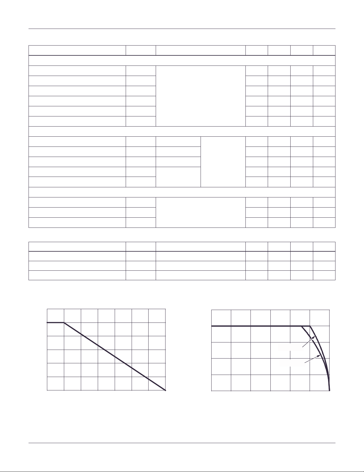
1.2
1.0
0.8
0.6
0.4
0.2
POWER DISSIPATION MULTIPLIER
0
0 25 50 75 100 150
TC, CASE TEMPERATURE (oC)
125 175
SD
rr
RR
ISD = 20A - - 1.25 V
ISD = 20A, dISD/dt = 100A/µs--58ns
ISD = 20A, dISD/dt = 100A/µs--70nC
25
20
15
10
, DRAIN CURRENT (A)
D
I
5
0
25 50 75 100 125 150 175
TC, CASE TEMPERATURE (oC)
VGS = 10V
VGS = 4.5V
FIGURE 1. NORMALIZED PO WER DISSIPATION vs CASE
TEMPERATURE
©2003 Fairchild Semiconductor Corporation HUF76121D3, HUF76121D3S Rev. B1
FIGURE 2. MAXIMUM CONTINUOUS DRAIN CURRENT vs
CASE TEMPERATURE
HUF76121D3, HUF76121D3S
Typical Performance Curves (Continued)
2
DUTY CYCLE - DESCENDING ORDER
0.5
1
0.2
0.1
0.05
0.02
0.01
0.1
, NORMALIZED
θJC
Z
THERMAL IMPEDANCE
0.01
-5
10
SINGLE PULSE
-4
10
10
FIGURE 3. NORMALIZED MAXIMUM TRANSIENT THERMAL IMPEDANCE
-3
10
-2
t, RECTANGULAR PULSE DURATION (s)
NOTES:
DUTY FACTOR: D = t
PEAK TJ = PDM x Z
-1
10
P
DM
t
1
t
2
1/t2
x R
JC
θ
0
10
+ T
JC
C
θ
1
10
1000
VGS = 10V
100
VGS = 5V
, PEAK CURRENT (A)
DM
I
TRANSCONDUCTANCE
MAY LIMIT CURRENT
IN THIS REGION
10
10
-5
10
-4
10
FIGURE 4. PEAK CURRENT CAPABILITY
500
100
10
, DRAIN CURRENT (A)
OPERATION IN THIS
D
I
AREA MAY BE
LIMITED BY r
BV
DSS MAX
1
DS(ON)
= 30V
1 10 100
V
, DRAIN TO SOURCE VOLTAGE (V)
DS
TJ = MAX RATED
= 25oC
T
C
100µs
1ms
10ms
FIGURE 5. FORWARD BIAS SAFE OPERATING AREA
TC = 25oC
-3
-2
10
-1
10
FOR TEMPERATURES
ABOVE 25
o
C DERATE PEAK
CURRENT AS FOLLOWS:
175 - T
I = I
25
0
10
C
150
1
10
t, PULSE WIDTH (s)
300
If R = 0
tAV = (L)(IAS)/(1.3*RATED BV
If R ≠ 0
100
= (L/R)ln[(IAS*R)/(1.3*RATED BV
t
AV
DSS
- VDD)
DSS
- VDD) +1]
STARTING TJ = 25oC
10
STARTING TJ = 150oC
, AVALANCHE CURRENT (A)
AS
I
1
0.001 0.01 0.1 1 10 100
tAV, TIME IN AVALANCHE (ms)
NO TE: Refer to Fairchild App lication Notes AN9321 and AN9322.
FIGURE 6. UNCLAMPED INDUCTIVE SWITCHING CAPABIL ITY
©2003 Fairchild Semiconductor Corporation HUF76121D3, HUF76121D3S Rev. B1
 Loading...