

Fairchild Semiconductor HUF76105SK8 Datasheet
Data Sheet January 2003
HUF76105SK8
5.5A, 30V, 0.050 Ohm, N-Channel, Logic
Level UltraFET Power MOSFET
This N-Channel powe r MOSFET i s
manufactured using the innovative
UltraFET™ process. This advanced
process technology achieves the
lowest possible on-resistance per silicon area, resulting in
outstanding performance. This device is capable of
withstanding high energy in the avalanche mode and the
diode exhibits very low reverse recovery time and stored
charge. It was designed for use in applications where power
efficiency is important, such as switching regulators, switching
converters, motor drivers, relay drivers, low-voltage bus
switches, and power management in portable and batteryoperated products.
Formerly developmental ty pe TA76105.
Ordering Information
PART NUMBER PACKAGE BRAND
HUF76105SK8 MS-012AA 76105SK8
NOTE: When ordering, use the e ntire part number. Add the suffix T
to obtain the variant in tape and reel, e.g., HUF76105SK8T.
Features
• Logic Level Gate Drive
• 5.5A, 30V
• Ultra Low On-Resistance, r
DS(ON)
= 0.050Ω
• Simulation Model s
®
- Temperature Compensated PSPICE
and SABER™
Electrical Models
- SPICE and SABER Thermal Impedance Models
Av ailable on the WEB at: www.fair childsemi.com
• Peak Current vs Pulse Width Curve
• UIS Rating Curve
• Transient Thermal Impedance Curve vs Board Mounting
Area
• Related Literature
- TB334, “Guidelines for Soldering Surface Mount
Components to PC Boards”
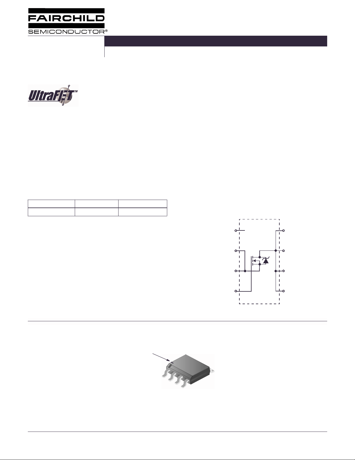
Symbol
NC(1)
DRAIN(8)
Packaging
JEDEC MS-012AA
BRANDING DASH
1
2
SOURCE(2)
SOURCE(3)
GATE(4)
5
3
4
DRAIN(7)
DRAIN(6)
DRAIN(5)
©2003 Fairchild Semiconductor Corporation HUF76105SK8 Rev. B1
HUF76105SK8
Absolute Maximum Ratings T
= 25oC, Unless Otherwise Specified
A
UNITS
Drain to Source Voltage (Note 1). . . . . . . . . . . . . . . . . . . . . . . . . . . . . . . . . . . . . . . . . . V
Drain to Gate Voltage (R
= 20kΩ) (Note 1) . . . . . . . . . . . . . . . . . . . . . . . . . . . . . . . . V
GS
Gate to Source Voltage . . . . . . . . . . . . . . . . . . . . . . . . . . . . . . . . . . . . . . . . . . . . . . . . . . V
DSS
DGR
GS
30 V
30 V
±20 V
Drain Current
Continuous (T
= 25oC, VGS = 10V) (Figure 2) (Note 2) . . . . . . . . . . . . . . . . . . . . . . . . . I
A
Continuous (TA= 100oC, VGS = 5V) (Note 3). . . . . . . . . . . . . . . . . . . . . . . . . . . . . . . . . . I
Continuous (TA= 100oC, VGS = 4.5V) (Note 3) . . . . . . . . . . . . . . . . . . . . . . . . . . . . . . . . I
Pulsed Drain Current . . . . . . . . . . . . . . . . . . . . . . . . . . . . . . . . . . . . . . . . . . . . . . . . . . .I
Pulsed Avalanche Rating. . . . . . . . . . . . . . . . . . . . . . . . . . . . . . . . . . . . . . . . . . . . . . . . . E
Power Dissipation (Note 2) . . . . . . . . . . . . . . . . . . . . . . . . . . . . . . . . . . . . . . . . . . . . . . . . P
Derate Above 25oC . . . . . . . . . . . . . . . . . . . . . . . . . . . . . . . . . . . . . . . . . . . . . . . . . . . . . . .
Operating and Storage Temperature . . . . . . . . . . . . . . . . . . . . . . . . . . . . . . . . . . . . T
, T
J
STG
D
D
D
DM
AS
D
5.5
1.4
1.3
Figure 4
Figures 6, 17, 18
2.5
20
-55 to 150
Maximum Temperature for Soldering
Leads at 0.063in (1.6mm) from Case for 10s. . . . . . . . . . . . . . . . . . . . . . . . . . . . . . . . . .T
Package Body for 10s, See Te chbrief 334 . . . . . . . . . . . . . . . . . . . . . . . . . . . . . . . . . . T
CAUTION: Stresses above those listed in “Absolute Maximum Rati ngs” may cause permane nt damage to the device. This is a stress only rating and oper ation of the
device at these or any other conditions above those indicated in the operational sections of this specification is not implied.
L
pkg
300
260
A
A
A
W
mW/oC
o
C
o
C
o
C
NOTES:
= 25oC to 125oC.
1. T
J
o
C/W measured using FR-4 boa rd at 1 seco nd.
2. 50
o
C/W measured using FR-4 board with 0.0115 in2 copper pad at 1000 seconds.
3. 212
Electrical Specifications T
= 25oC, Unless Ot herwise Specified
A
PARAMETER SYMBOL TEST CONDITIONS MIN TYP MAX UNITS
OFF STATE SPECIFICATIONS
Drain t o Source Breakdown Voltage BV
Zero Gat e V ol tag e D rain Current I
Gate to Sour c e Le ak ag e C urr e nt I
ON STATE SPECIFICATIONS
Gate to Source Threshold Voltage V
Drain to Source On Resistance r
GS(TH)VGS
DS(ON)ID
THERMAL SPECIFICATIONS
Thermal Resistance Junction to Ambient R
SWITCHING SPECIFICATIONS (V
GS
= 4.5V)
Turn-On Time t
Turn-On Delay Time t
d(ON)
Rise Time t
Turn-Off Delay Time t
d(OFF)
Fall Time t
Turn-Off Time t
DSSID
DSS
GSS
θJA
ON
r
f
OFF
= 250µA, VGS = 0V (Figure 12) 30 - - V
VDS = 25V, VGS = 0V - - 1 µA
V
= 25V, VGS = 0V, TC = 150oC--250µA
DS
VGS = ±20V - - ±100 nA
= VDS, ID = 250µA (Figure 11) 1 - 3 V
= 5.5A, VGS = 10V (Figures 9, 10) - 0.040 0.050 Ω
I
= 1.4A, VGS = 5V (Figure 9) - 0.055 0.072 Ω
D
I
= 1.3A, VGS = 4.5V (F igure 9) - 0.060 0.078 Ω
D
Pad Area = 0.76 in2 (Note 2) - - 50
Pad Area = 0.054 in
Pad Area = 0.0115 in
VDD = 15V, ID ≅ 1.3 A, RL = 11.5Ω,
V
= 4.5V, RGS = 27Ω
GS
(Figures 15, 2 1, 22)
2
(Figure 23) - - 175
2
(Figure 23) - - 212
- - 60 ns
-12-ns
o
o
o
C/W
C/W
C/W
-28-ns
-31-ns
-21-ns
- - 80 ns
©2003 Fairchild Semiconductor Corporation HUF76105SK8 Rev. B1
HUF76105SK8
Electrical Specifications T
= 25oC, Unless Ot herwise Specified
A
PARAMETER SYMBOL TEST CONDITIONS MIN TYP MAX UNITS
SWITCHING SPECIFICATIONS (VGS = 10V)
Turn-On Time t
Turn-On Delay Time t
Rise Time t
Turn-Off Delay Time t
Fall Time t
Turn-Off Time t
GATE CHARGE SPECIFICATIONS
Total Gate Charg e Q
Gate Charge at 5V Q
Threshold Gate Ch arg e Q
Gate to Source Gate Charg e Q
Reverse Transfer Capacitance Q
CAPACITANCE SPECIFICATIONS
Input Capacitance C
Output Capacitance C
Reverse Transfer Capacitance C
ON
d(ON)
d(OFF)
OFF
g(TOT)VGS
g(5)
g(TH)
ISS
OSS
RSS
VDD = 15V, ID ≅ 5.5 A, RL = 2.7Ω,
V
R
(Figures 16, 2 1, 22)
r
f
VGS = 0V to 5V - 5.3 6.4 nC
VGS = 0V to 1V - 0.35 0.45 nC
gs
gd
VDS = 25V, VGS = 0V,
f = 1MHz
(Figure 13)
= 10V,
GS
= 27Ω
GS
= 0V to 10V VDD = 15V, ID ≅ 1.4A,
R
= 10.7Ω
L
I
= 1.0mA
g(REF)
(Figures 14, 19, 20)
- - 60 ns
-17-ns
-21-ns
-60-ns
- 20 - ns
--120ns
-911nC
-0.8-nC
-2.5-nC
-325- pF
-180- pF
-35-pF
Source to Drain Diode Specifications
PARAMETER SYMBOL TEST CONDITIONS MIN TYP MAX UNITS
Source to Drain Diode Vol tage V
Reverse Recovery Time t
Reverse Recovered Charge Q
Typical Performance Curves
1.2
1.0
0.8
0.6
0.4
0.2
POWER DISSIPATION MULTIPLIER
0
0 25 50 75 100 150
TA, AMBIENT TEMPERATURE (oC)
SD
rr
RR
ISD = 5.5A - - 1.25 V
= 1.4A 1.00 V
I
SD
ISD = 1.4A, dISD/dt = 100A/µs--39ns
ISD = 1.4A, dISD/dt = 100A/µs--42nC
6
5
V
125
= 10V, R
4
3
2
, DRAIN CURRENT (A)
D
I
V
1
0
25
= 4.5V, R
GS
50 75 100 125 150
= 212oC/W
θJA
TA, AMBIENT TEMPERATURE (oC)
GS
θJA
= 50oC/W
FIGURE 1. NORMALIZED POWER DISSIPA TION vs AMBIE NT
TEMPERATURE
©2003 Fairchild Semiconductor Corporation HUF76105SK8 Rev. B1
FIGURE 2. MAXIMUM CONTINUOUS DRAIN CURRENT vs
AMBIENT TEMPERATURE
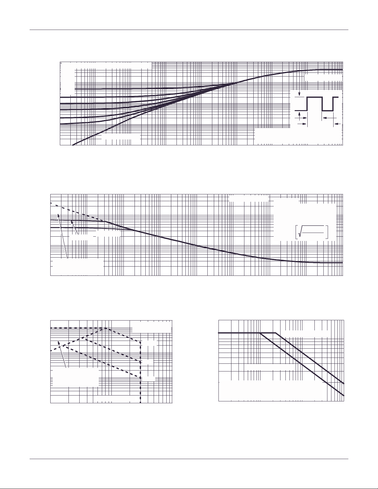
Typical Performance Curves (Continued)
10
DUTY CYCLE - DESCENDING ORDER
0.5
0.2
0.1
0.05
1
0.02
0.01
0.1
, NORMALIZED
θJA
Z
THERMAL IMPEDANCE
0.01
SINGLE PULSE
0.001
-5
10
-4
10
-3
10
FIGURE 3. NORMALIZED MAXIMUM TRANSIENT THERMAL IMPEDANCE
HUF76105SK8
-2
10
t, RECTANGULAR PULSE DURATION (s)
-1
10
10
NOTES:
DUTY FACTOR: D = t
PEAK TJ = PDM x Z
0
R
= 50oC/W
θJA
P
DM
t
1
t
2
1/t2
x R
θJA
1
10
+ T
θJA
A
2
10
10
3
500
100
VGS = 10V
VGS = 5V
10
, PEAK CURRENT (A)
DM
I
TRANSCONDUCTANCE
MAY LIMIT CURRENT
IN THIS REGION
1
-5
10
-4
10
10
-3
FIGURE 4. PEAK CURRENT CAPABILITY
200
100
10
OPERATION IN THIS
AREA MAY BE
1
, DRAIN CURRENT (A)
I
D
0.1
LIMITED BY r
1
ds(ON)
BV
DSS MAX
10 100
V
, DRAIN TO SOURCE VOLTAGE (V)
DS
TJ = MAX RATED
T
A
= 30V
= 25oC
100µs
1ms
10ms
FIGURE 5. FORWARD BIAS SAFE OPERATING AREA
R
= 50oC/W
θJA
TC = 25oC
FOR TEMPERATURE S
ABOVE 25
o
C DERATE PEAK
CURRENT AS FOLLOWS:
150 - T
I = I
25
-2
10
-1
10
0
10
1
10
A
125
2
10
10
3
t, PULSE WIDTH (s)
20
10
STARTING TJ = 25oC
STARTING TJ = 150oC
If R = 0
, AVALANCHE CURRENT (A)
tAV = (L)(IAS)/(1.3* R ATED BV
AS
I
≠
0
If R
t
= (L/R) ln[(IAS*R)/(1.3*RATED B V
AV
1
DSS
- VDD)
DSS
- VDD) +1]
0.01 0.1 1 10
tAV, TIME IN AVALANCHE (ms)
NO TE: Refer to Fairchild Application Notes AN9321 and AN9322.
FIGURE 6. UNCLAMPED INDUCTIVE SWITCHING
CAPABILITY
©2003 Fairchild Semiconductor Corporation HUF76105SK8 Rev. B1
 Loading...