

Fairchild Semiconductor HUF76013D3S, HUF76013P3 Datasheet
Data Sheet December 2001
20A, 20V, 0.022 Ohm, N-Channel, Logic
Level Power MOSFETs
The HUF76013 is an application-specific MOSFET
optimized fo r switching when used as the upper switch in
synchronous bu ck appl ications . The low gate charge and low
input capacitance results in lower driver and lower switching
losses thereby increasing the overall sy stem efficiency.
Symbol
D
G
S
Packaging
HUF76013D3S
JEDEC TO-252AA
DRAIN (FLANGE)
GATE
SOURCE
HUF76013P3
JEDEC TO-220AB
SOURCE
DRAIN
(FLANGE)
DRAIN
GATE
HUF76013P3, HUF76013D3S
Features
• 20A, 20V
-r
-r
• PWM Optimiz ed for Synchronous Buck Applications
•Fast Switching
• Low Gate Charge
-Q
• Low Capacitance
-C
-C
Ordering Information
PART NUMBER PACKAGE BRAND
HUF76013P3 TO-220AB 76013P
HUF76013D3S TO-252AA 76013D
NOTE: When ordering, use the entire part number. Add the suffix T to
obtain the HUF76013D3S in tape and reel, e.g., HUF 760 13D3ST.
= 0.022Ω, V
DS(ON)
= 0.030Ω, V
DS(ON)
Total 14nC (Typ)
g
624pF (Typ)
ISS
71pF (Typ)
RSS
GS
GS
= 10V
= 5V
Absolute Maximum Ratings
SYMBOL PARAMETER
V
DSS
V
DGR
V
GS
I
D
I
D
I
DM
P
D
T
, T
J
STG
T
L
T
pkg
THERMAL SPECIFICATIONS
R
θJC
R
θJA
NOTE:
= 25oC to 125oC.
1. T
J
CAUTION: Stresses above those listed in “ Absolute M aximum Ratings” may cause perm anent damage to th e device. This is a stress onl y rating and operation of the
device at these or any other conditions above those indicated in the operational sections of this specification is not implied.
Drain to Source Voltage (Note 1) 20 V
Drain to Gate Voltage (RGS = 20kΩ) (Note 1) 20 V
Gate to Source Voltage ±16 V
Drain Current
Continuous (T
Continuous (T
Pulsed Drain Current
Power Dissipation
Derate Above 25
Operating and Storage Temperature -55 to 150
Maximum Temperature for Soldering
Leads at 0.063in (1.6mm) from Case for 10s
Package Body for 10s, See Techbrief TB334
Thermal Resistance Junction to Case, TO-220, TO-252 2.5
Thermal Resistance Junction to Ambient TO-220 62
Thermal Resistance Junction to Ambient TO-252 100
TC = 25oC, Unless Otherwise Specified
= 25oC, VGS = 10V) (Figure 2)
C
= 100oC, VGS = 5V)
C
o
C
HUF76013P3,
HUF76013D3S UNITS
20
20
Figure 4
50
0.4
300
260
A
A
A
W
W/oC
o
C
o
C
o
C
o
C/W
o
C/W
o
C/W
©2001 Fairchild Semiconductor Corpo ration HUF76013P3, HUF76013D3S Rev. B
HUF76013P3, HUF76013D3S
Electrical Specifications
TC = 25oC, Unless Otherwise Specified
PARAMETER SYMBOL TEST CONDITIONS MIN TYP MAX UNITS
OFF STATE SPECIFICATIONS
Drain to Source Breakdown Voltage BV
Zero Gate Voltage Drain Current I
Gate to Source Leakage Current I
ON STATE SPECIFICATIONS
Gate to Source Threshold Voltage V
Drain to Source ON Resistance r
SWITCHING SPECIFICATIONS (V
GS
= 5V)
Turn-On Time t
Turn-On Delay Time t
Rise Time t
Turn-Off Delay Time t
Fall Time t
Turn-Off Time t
SWITCHING SPECIFICATIONS (V
GS
= 10V)
Turn-On Time t
Turn-On Delay Time t
Rise Time t
Turn-Off Delay Time t
Fall Time t
Turn-Off Time t
GATE CHARGE SPECIFICATIONS
Total Gate Charge at 10V Q
Total Gate Charge at 5V Q
Threshold Gate Charge Q
Gate to Source Gate Charge Q
Gate to Drain “Miller” Charge Q
CAPACITANCE SPECIFICATIONS
Input Capacitance C
Output Capacitance C
Reverse Transfer Capacitance C
DSSID
DSS
GSS
GS(TH)VGS
DS(ON)ID
ON
d(ON)
d(OFF)
OFF
ON
d(ON)
d(OFF)
OFF
g(TOT)VGS
g(TOT)VGS
g(TH)
ISS
OSS
RSS
VDS = 20V, VGS = 0V - - 1 µA
V
DS
VGS = ±16V - - ±100 nA
I
D
VDD = 10V, ID = 20A
V
GS
(Figures 14, 18, 19)
r
f
VDD = 10V, ID = 20A
V
GS
R
r
f
GS
(Figures 15, 18, 19)
VGS = 0V to 1V - 0.9 1 nC
gs
gd
VDS = 20V, VGS = 0V,
f = 1MHz
(Figure 12)
= 250µA, VGS = 0V (Figure 11) 20 - - V
= 20V, VGS = 0V, TC = 150oC - - 250 µA
= VDS, ID = 250µA (Figure 10) 1 - 3 V
= 20A, VGS = 10V (Figures 8, 9) - 0.018 0.022 Ω
= 20A, VGS = 5V (Figure 8) - 0.025 0.030 Ω
- - 197 ns
= 5V, RGS = 19Ω
-11-ns
- 120 - ns
-19-ns
-30-ns
- - 72 ns
- - 151 ns
= 10V,
= 19Ω
-7-ns
-93-ns
-37-ns
-29-ns
- - 100 ns
= 0V to 10V VDD = 10V,
= 20A,
I
= 0V to 5V - 7.8 9 nC
D
I
g(REF)
= 1.0mA
- 14.4 17 nC
(Figures 13, 16, 17)
-3.5-nC
-3.2-nC
- 624 - pF
- 444 - pF
-71-pF
Source to Drain Diode Specifications
PARAMETER SYMBOL TEST CONDITIONS MIN TYP MAX UNITS
Source to Drain Diode Voltage V
Reverse Recovery Time t
Reverse Recovered Charge Q
©2001 Fairchild Semiconductor Corpo ration HUF76013P3, HUF76013D3S Rev. B
SD
rr
RR
I
= 20A - - 1.25 V
SD
= 10A - - 1.0 V
I
SD
ISD = 20A, dISD/dt = 100A/µs--55ns
ISD = 20A, dISD/dt = 100A/µs--82nC
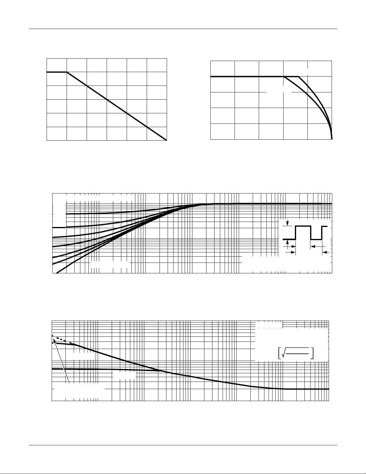
Typical Performance Curves
0
0
HUF76013P3, HUF76013D3S
1.2
1.0
0.8
0.6
0.4
0.2
POWER DISSIPATION MULTIPLIER
0
0 25 50 75 100 15
125
TA, AMBIENT TEMPERATURE (oC)
FIGURE 1. NORMALIZED POWER DISSIPATION vs CASE
TEMPERATURE
2
DUTY CYCLE - DESCENDING ORDER
0.5
1
0.2
0.1
0.05
0.02
0.01
0.1
, NORMALIZED
θJC
Z
THERMAL IMPEDANCE
SINGLE PULSE
0.01
-5
10
-4
10
-3
10
t, RECTANGULAR PULSE DURATION (s)
25
20
V
= 5.0V
15
GS
10
, DRAIN CURRENT (A)
D
I
5
0
25 50 75 100 125 15
TC, CASE TEMPERATURE (oC)
FIGURE 2. MAXIMUM CONTINUOUS DRAIN CURRENT vs
CASE TEMPERATURE
P
DM
NOTES:
DUTY FACTOR: D = t1/t
PEAK TJ = PDM x Z
-2
10
-1
10
θJC
10
x R
0
2
+ T
θJC
V
= 10V
GS
t
1
t
2
C
1
10
FIGURE 3. NORMALIZED MAXIMUM TRANSIENT THERMAL IMPEDANCE
, PEAK CURRENT (A)
I
DM
1000
100
TRANSCONDUCTANCE
MAY LIMIT CURRENT
IN THIS REGION
10
-5
10
VGS = 10V
VGS = 5V
-4
10
-3
10
-2
10
-1
10
t, PULSE WIDTH (s)
TC = 25oC
FOR TEMPERATURES
ABOVE 25
o
C DERATE PEAK
CURRENT AS FOLLOWS:
150 - T
I = I
25
10
C
125
0
1
10
FIGURE 4. PEAK CURRENT CAPAB ILITY
©2001 Fairchild Semiconductor Corpo ration HUF76013P3, HUF76013D3S Rev. B
 Loading...