

Fairchild Semiconductor HRFZ44N Datasheet
D
G
S
HRFZ44N
Data Sheet December 2001
49A, 55V, 0.022 Ohm, N-Channel UltraFET
Power MOSFET
This N-Channel power MOSFET is
manufactured using the innovative
UltraFET™ process. This advanced
process technology achieves the
lowest possible on-resistance per silicon area, resulting in
outstanding performance. This device is capable of
withstanding high energy in the avalanche mode and the
diode exhibits very low reverse recovery time and stored
charge. It was designed for use in applications where power
efficiency is important, such as switching regulators,
switching converters, motor drivers, relay drivers, lowvoltage bus switches, and power management in portable
and battery-operated products.
Formerly developmental type TA75329.
Ordering Information
PART NUMBER PACKAGE BRAND
HRFZ44N TO-220AB HRFZ44N
NOTE: When ordering, use the entire part number.
Features
• 49A, 55V
• Simulation Models
- Temperature Compensated PSPICE
Electrical Models
- Spice and Saber Thermal Impedance Models
- www.Fairchild.com
• Peak Current vs Pulse Width Curve
• UIS Rating Curve
• Related Literature
- TB334, “Guidelines for Soldering Surface Mount
Components to PC Boards”
®
and SABER
Symbol
©
Packaging
JEDEC TO-220AB
SOURCE
DRAIN
GATE
DRAIN
(FLANGE)
©2001 Fairchild Semiconductor Corporation HRFZ44N Rev. B
±
µ
µ
±
Ω
θ
θ
≅
=
≅
HRFZ44N
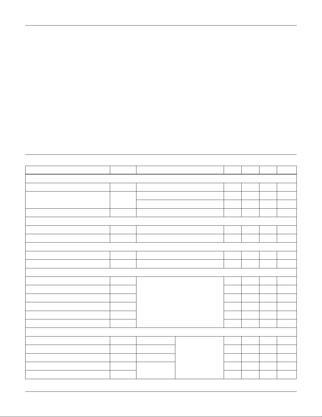
Absolute Maximum Ratings
o
T
= 25
C, Unless Otherwise Specified
C
UNITS
Drain to Source Voltage (Note 1) . . . . . . . . . . . . . . . . . . . . . . . . . . . . . . . . . . . . . . . . . . V
Drain to Gate Voltage (R
= 20k Ω ) (Note 1) . . . . . . . . . . . . . . . . . . . . . . . . . . . . . . . . V
GS
Gate to Source Voltage . . . . . . . . . . . . . . . . . . . . . . . . . . . . . . . . . . . . . . . . . . . . . . . . . . V
DSS
DGR
GS
55 V
55 V
20 V
Drain Current
Continuous (Figure 2). . . . . . . . . . . . . . . . . . . . . . . . . . . . . . . . . . . . . . . . . . . . . . . . . . . . I
Pulsed Drain Current (Note 2) . . . . . . . . . . . . . . . . . . . . . . . . . . . . . . . . . . . . . . . . . . . . I
D
DM
Pulsed Avalanche Rating. . . . . . . . . . . . . . . . . . . . . . . . . . . . . . . . . . . . . . . . . . . . . . . . . . UIS 0.227 A
Power Dissipation . . . . . . . . . . . . . . . . . . . . . . . . . . . . . . . . . . . . . . . . . . . . . . . . . . . . . . . P
Derate Above 25
o
C . . . . . . . . . . . . . . . . . . . . . . . . . . . . . . . . . . . . . . . . . . . . . . . . . . . . . . .
Operating and Storage Temperature . . . . . . . . . . . . . . . . . . . . . . . . . . . . . . . . . . . . T
D
, T
J
STG
Maximum Temperature for Soldering
Leads at 0.063in (1.6mm) from Case for 10s. . . . . . . . . . . . . . . . . . . . . . . . . . . . . . . . . . T
Package Body for 10s, See Techbrief 334 . . . . . . . . . . . . . . . . . . . . . . . . . . . . . . . . . . T
CAUTION: Stresses above those listed in “Absolute Maximum Ratings” may cause permanent damage to the device. This is a stress only rating and operation of the
device at these or any other conditions above those indicated in the operational sections of this specification is not implied.
L
pkg
49
160
120
0.8
-55 to 175
300
260
W/
A
A
2
s
W
o
C
o
C
o
C
o
C
NOTE:
1. T
= 25
J
o
C to 150
o
C.
2. Repetitive rating: pulse width limited by maximum junction temperature.
Electrical Specifications
o
T
= 25
C, Unless Otherwise Specified
C
PARAMETER SYMBOL TEST CONDITIONS MIN TYP MAX UNITS
OFF STATE SPECIFICATIONS
Drain to Source Breakdown Voltage BV
Zero Gate Voltage Drain Current I
Gate to Source Leakage Current I
DSS
GSS
DSS
I
= 250 µ A, V
D
V
= 50V, V
DS
V
= 45V, V
DS
V
= ± 20V - -
GS
= 0V (Figure 11) 55 - - V
GS
= 0V - - 1
GS
GS
= 0V, T
= 150
C
o
C - - 250
A
A
100 nA
ON STATE SPECIFICATIONS
Gate to Source Threshold Voltage V
Drain to Source On Resistance r
GS(TH)
DS(ON)
V
= V
GS
I
= 25A, V
D
, I
= 250 µ A (Figure 10) 2 - 4 V
DS
D
= 10V (Figure 9) - 0.019 0.022
GS
THERMAL SPECIFICATIONS
Thermal Resistance Junction to Case R
Thermal Resistance Junction to Ambient R
SWITCHING SPECIFICATIONS (V
GS
= 10V)
Turn-On Time t
Turn-On Delay Time t
d(ON)
Rise Time t
Turn-Off Delay Time t
d(OFF)
Fall Time t
Turn-Off Time t
ON
r
f
OFF
(Figure 3) - - 1.25
JC
TO-220 - - 62
JA
V
= 30V, I
DD
R
= 1.2 Ω , V
L
R
= 9.1 Ω
GS
D
GS
25A,
10V,
- - 105 ns
-12- ns
-58- ns
-33- ns
-33- ns
- - 100 ns
o
C/W
o
C/W
GATE CHARGE SPECIFICATIONS
Total Gate Charge Q
Gate Charge at 10V Q
Threshold Gate Charge Q
Gate to Source Gate Charge Q
Gate to Drain “Miller” Charge Q
g(TOT)
g(10)
g(TH)
gs
gd
V
= 0V to 20V V
GS
V
= 0V to 10V - 35 43 nC
GS
V
= 0V to 2V - 2.0 2.5 nC
GS
= 30V,
DD
I
25A,
D
R
= 1.2 Ω
L
I
= 1.0mA
g(REF)
(Figure 13)
-6075nC
-4-nC
-14- nC
©2001 Fairchild Semiconductor Corporation HRFZ44N Rev. B
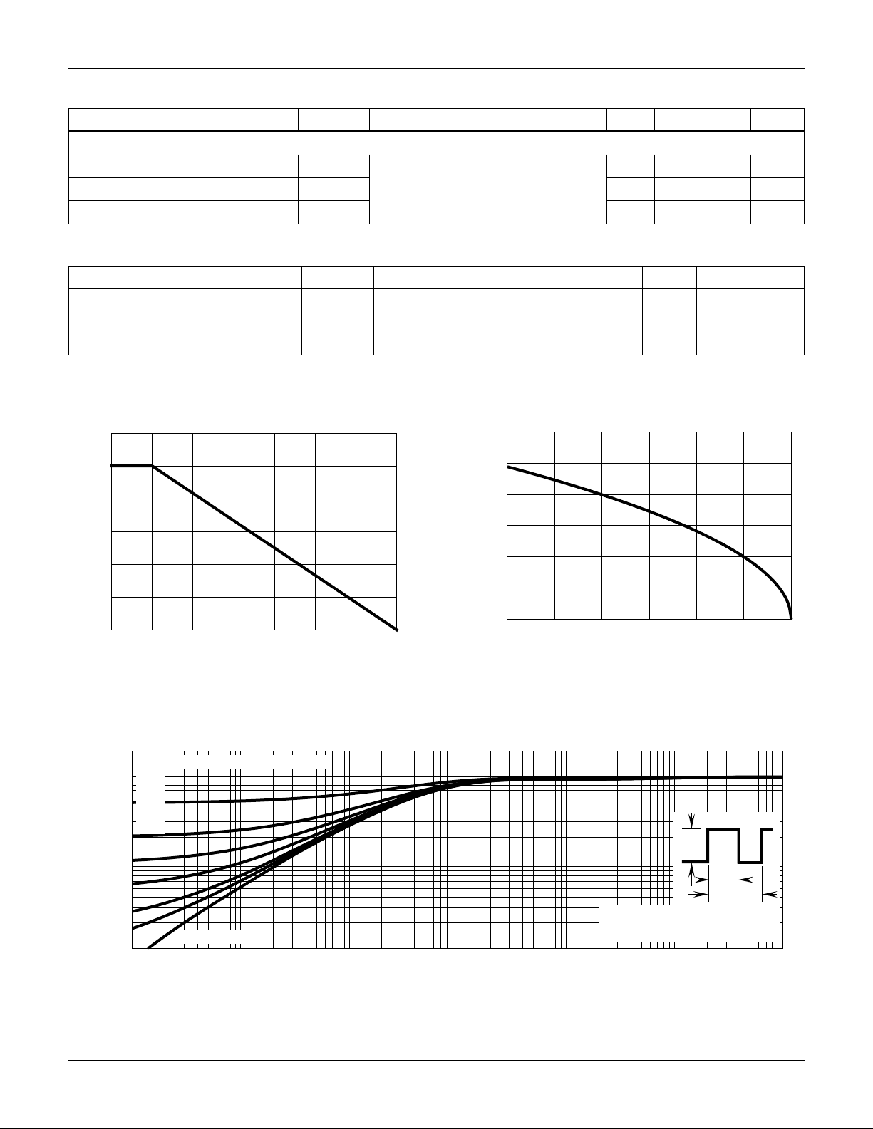
I
D
, DRAIN CURRENT (A)
TC, CASE TEMPERATURE (oC)
10
20
30
50
50 75 100 125 150 175
0
25
40
60
HRFZ44N
Electrical Specifications
o
T
= 25
C, Unless Otherwise Specified
C
PARAMETER SYMBOL TEST CONDITIONS MIN TYP MAX UNITS
CAPACITANCE SPECIFICATIONS
Input Capacitance C
Output Capacitance C
Reverse Transfer Capacitance C
Source to Drain Diode Specifications
PARAMETER SYMBOL TEST CONDITIONS MIN TYP MAX UNITS
Source to Drain Diode Voltage V
Reverse Recovery Time t
Reverse Recovered Charge Q
Typical Performance Curves
1.2
1.0
0.8
ISS
OSS
RSS
SD
rr
RR
V
= 25V, V
DS
(Figure 12)
= 0V, f = 1MHz
GS
- 1060 - pF
- 405 - pF
-95- pF
I
= 25A - - 1.25 V
SD
I
= 25A, dI
SD
I
= 25A, dI
SD
/dt = 100A/ µ s--72ns
SD
/dt = 100A/ µ s - - 120 nC
SD
0.6
0.4
0.2
POWER DISSIPATION MULTIPLIER
0
0 25 50 75 100 150
TC, CASE TEMPERATURE (oC)
125
FIGURE 1. NORMALIZED POWER DISSIPATION vs CASE
TEMPERATURE
2
DUTY CYCLE - DESCENDING ORDER
0.5
1
0.2
0.1
0.05
0.02
0.01
0.1
, NORMALIZED
θJC
Z
THERMAL IMPEDANCE
0.01
-5
10
SINGLE PULSE
-4
10
10
175
FIGURE 2. MAXIMUM CONTINUOUS DRAIN CURRENT vs
-3
t, RECTANGULAR PULSE DURATION (s)
-2
10
CASE TEMPERATURE
NOTES:
DUTY FACTOR: D = t
PEAK TJ = PDM x Z
-1
10
P
DM
t
1
t
2
1/t2
x R
θJC
+ T
C
1
10
θJC
0
10
©2001 Fairchild Semiconductor Corporation HRFZ44N Rev. B
FIGURE 3. NORMALIZED MAXIMUM TRANSIENT THERMAL IMPEDANCE
 Loading...