Fairchild Semiconductor HPLR3103 Datasheet

D
G
S
DRAIN
(FLANGE)
GATE
SOURCE
HPLR3103, HPLU3103
Data Sheet December 2001
52A, 30V, 0.019 Ohm, N-Channel Logic
Level, Power MOSFETs
These are N-Channel enhancement mode silicon gate
power field effect transistors. They are advanced power
MOSFETs designed, tested, and guaranteed to withstand a
specified level of energy in the breakdown avalanche mode
of operation. All of these power MOSFETs are designed for
applications such as switching regulators, switching
converters, motor drivers, relay drivers, and drivers for high
power bipolar switching transistors requiring high speed and
low gate drive power. These types can be operated directly
from integrated circuits.
Ordering Information
PART NUMBER PACKAGE BRAND
HPLU3103 TO-251AA HP3103
HPLR3103 TO-252AA HP3103
NOTE: When ordering, use the entire part number. Add the suffix T
to obtain the TO-252AA variant in tape and reel, e.g., HPLR3103T.
Packaging
Features
• Logic Level Gate Drive
• 52A † , 30V
• Low On-Resistance, r
• UIS Rating Curve
• Related Literature
- TB334, “Guidelines for Soldering Surface Mount
Components to PC Boards”
†
Calculated continuous current based on maximum allowable junction
temperature. Package limited to 20A continuous, see Figure 9.
DS(ON)
= 0.019 Ω
Symbol
DRAIN
(FLANGE)
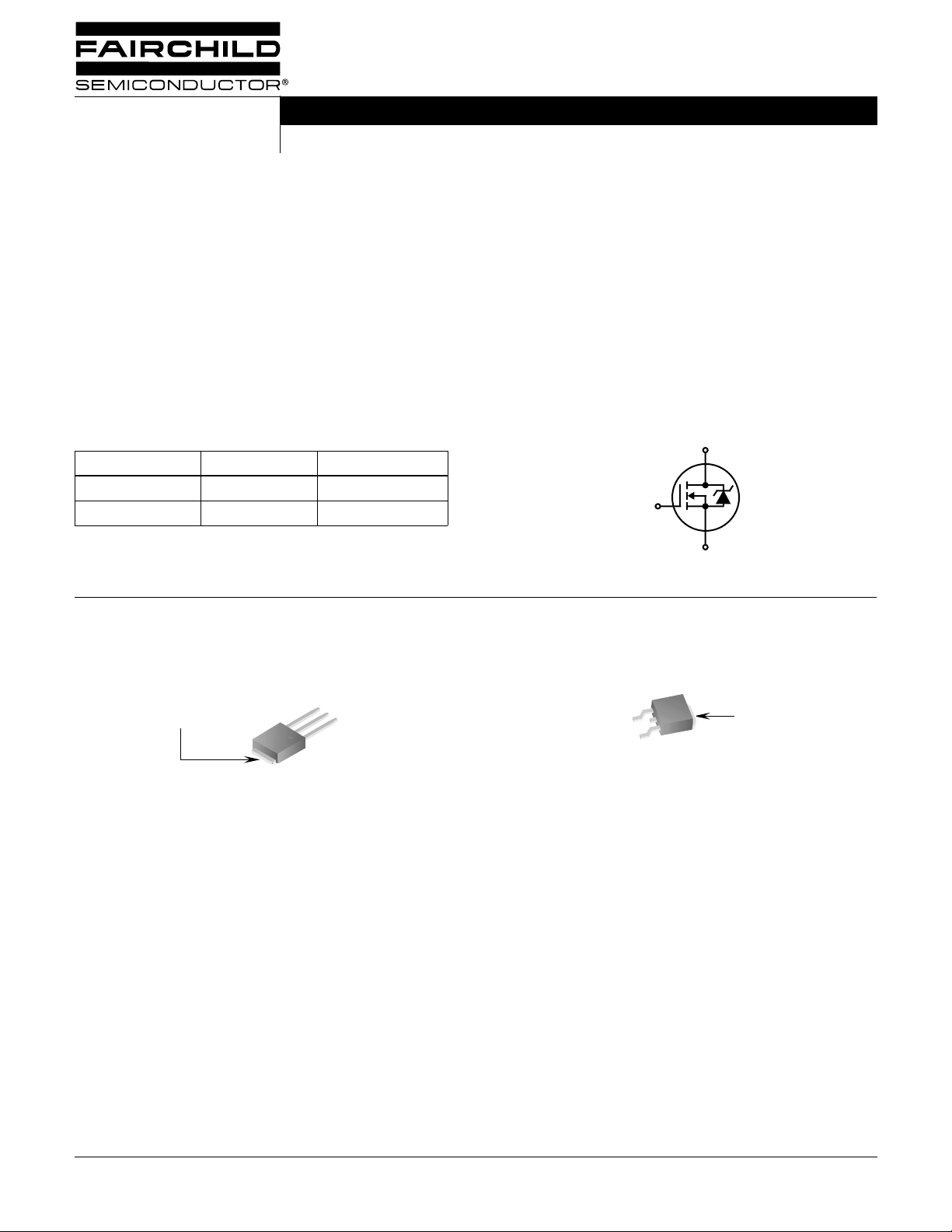
JEDEC TO-251AA JEDEC TO-252AA
SOURCE
DRAIN
GATE
©2001 Fairchild Semiconductor Corporation HPLR3103, HPLU3103 Rev. B

±
µ
µ
∆
/ ∆
≅
=
≅
HPLR3103, HPLU3103
Absolute Maximum Ratings
o
T
= 25
C, Unless Othewise Specified
C
HPLR3103, HPLU3103 UNITS
Drain to Source Voltage (Note 1) . . . . . . . . . . . . . . . . . . . . . . . . . . . . . . . . . . . . . . . . . . V
Drain to Gate Voltage (R
Gate to Source Voltage . . . . . . . . . . . . . . . . . . . . . . . . . . . . . . . . . . . . . . . . . . . . . . . . . . V
= 20k Ω ) (Note 1) . . . . . . . . . . . . . . . . . . . . . . . . . . . . . . . V
GS
Continuous Drain Current . . . . . . . . . . . . . . . . . . . . . . . . . . . . . . . . . . . . . . . . . . . . . . . . . . I
Pulsed Drain Current (Note 2) . . . . . . . . . . . . . . . . . . . . . . . . . . . . . . . . . . . . . . . . . . . . . .I
Single Pulse Avalanche Energy (Note 4). . . . . . . . . . . . . . . . . . . . . . . . . . . . . . . . . . . . . E
Power Dissipation . . . . . . . . . . . . . . . . . . . . . . . . . . . . . . . . . . . . . . . . . . . . . . . . . . . . . . . P
Derate Above 25
o
C . . . . . . . . . . . . . . . . . . . . . . . . . . . . . . . . . . . . . . . . . . . . . . . . . . . . . . .
Operating and Storage Temperature . . . . . . . . . . . . . . . . . . . . . . . . . . . . . . . . . . . . T
Maximum Temperature for Soldering
Leads at 0.063in (1.6mm) from Case for 10s. . . . . . . . . . . . . . . . . . . . . . . . . . . . . . . . . . T
Package Body for 10s, See Techbrief 334 . . . . . . . . . . . . . . . . . . . . . . . . . . . . . . . . . . T
CAUTION: Stresses above those listed in “Absolute Maximum Ratings” may cause permanent damage to the device. This is a stress only rating and operation of the
device at these or any other conditions above those indicated in the operational sections of this specification is not implied.
DSS
DGR
GS
D
DM
AS
D
, T
J
STG
L
pkg
30 V
30 V
16V V
52
390
240 mj
89
0.71
-55 to 150
300
260
W/
A
A
W
o
C
o
C
o
C
o
C
NOTE:
= 25
J
o
1. T
Electrical Specifications
C to 125
o
C.
o
T
= 25
C, Unless Otherwise Specified
C
PARAMETER SYMBOL TEST CONDITIONS MIN TYP MAX UNITS
Drain to Source Breakdown Voltage BV
Gate to Source Threshold Voltage V
GS(TH)
Zero Gate Voltage Drain Current I
Gate to Source Leakage Current I
Breakdown Voltage Temperature
Coefficient
Drain to Source On Resistance
(Note 3)
Turn-On Delay Time t
V
(BR)DSS
r
DS(ON)
d(ON)
Rise Time t
Turn-Off Delay Time (Note 3) t
d(OFF)
Fall Time t
Total Gate Charge Q
Gate to Source Charge Q
Gate to Drain “Miller” Charge Q
Input Capacitance C
Output Capacitance C
Reverse Transfer Capacitance C
Internal Source Inductance L
Internal Drain Inductance L
DSS
GSS
OSS
RSS
I
DSS
= 250 µ A, V
D
V
= V
GS
DS
V
= 30V, V
DS
V
= 24V, V
DS
V
= ± 16V - - 100 nA
GS
Reference to 25
T
J
I
= 28A, V
D
I
= 23A, V
D
V
= 15V, I
DD
R
=3.4 Ω, I
r
f
g
gs
gd
ISS
GS
V
= 24V
DD
I
34A,
D
V
= 4.5V
GS
(Figure 6)
V
= 25V, V
DS
f = 1MHz (Figure 5)
Measured From the
S
Source Lead, 6mm (0.25in)
From Package to Center of
Die
Measured From the Drain-
D
Lead, 6mm (0.25in) From
= 0V 30 - - V
GS
, I
= 250 µ A1--V
D
= 0V - - 25
GS
= 0V, T
GS
o
C, I
= 1mA - 0.037 - V
D
= 10V - - 0.019 Ω
GS
= 4.5V - - 0.024 Ω
GS
34A, R
D
g(REF)
L
= 3mA
o
= 125
C
C - - 250
= 0.441 Ω , V
GS
4.5V,
-9 - ns
- 210 - ns
A
A
-20 - ns
-54 - ns
- - 50 nC
- - 14 nC
- - 28 nC
GS
= 0V,
- 1600 - pF
- 640 - pF
- 320 - pF
Modified MOSFET
- 7.5 - nH
Symbol Showing
the Internal Devices Inductances
D
L
D
- 4.5 - nH
Package to Center of Die
G
L
S
S
©2001 Fairchild Semiconductor Corporation HPLR3103, HPLU3103 Rev. B

1
100
1000
0.1 1 10 100
20µs PULSE WIDTH
T
C
= 150oC
V
DS
, DRAIN TO SOURCE VOLTAGE (V)
I
D
, DRAIN TO SOURCE CURRENT (A)
12V
10V
8.0V
6.0V
4.0V
3.0V
2.5V
15V
V
GS
IN DECENDING ORDER
10
HPLR3103, HPLU3103
θ
θ
Electrical Specifications
T
o
= 25
C, Unless Otherwise Specified
C
PARAMETER SYMBOL TEST CONDITIONS MIN TYP MAX UNITS
Thermal Resistance Junction to Case R
Thermal Resistance Junction to Ambient R
JC
JA
(PCB Mount Steady State) - - 50
Source to Drain Diode Specifications
PARAMETER SYMBOL TEST CONDITIONS MIN TYP MAX UNITS
Continuous Source to Drain Current I
Pulsed Source to Drain Current (Note 2) I
Source to Drain Diode Voltage (Note 3) V
SD
SDM
SD
Reverse Recovery Time (Note 3) t
Reverse Recovered Charge (Note 3) Q
RR
NOTES:
2. Repetitive rating; pulse width limited by maximum junction temperature (See Figure 11).
3. Pulse width ≤ 300 µ s; duty cycle ≤ 2%.
4. V
= 15V, starting T
DD
o
= 25
C, L = 300 µ H, R
J
= 25 Ω , peak I
G
MOSFET
Symbol Showing
The Integral
Reverse P-N
Junction Diode
I
= 28A - - 1.3 V
SD
I
rr
= 34A, dI
SD
I
= 34A, dI
SD
= 34A, (Figure 10).
AS
/dt = 100A/ µ s - 81 120 ns
SD
/dt = 100A/ µ s - 210 310 nC
SD
- - 1.4
- - 110
D
- - 52 (Note 1)A
o
C/W
o
C/W
o
C/W
- - 220 A
G
S
Typical Performance Curves
1000
V
IN DECENDING ORDER
GS
15V
12V
10V
8.0V
100
6.0V
4.0V
3.0V
2.5V
10
, DRAIN TO SOURCE CURRENT (A)
D
I
1
0.1 1.0 10 100
V
, DRAIN TO SOURCE VOLTAGE (V)
DS
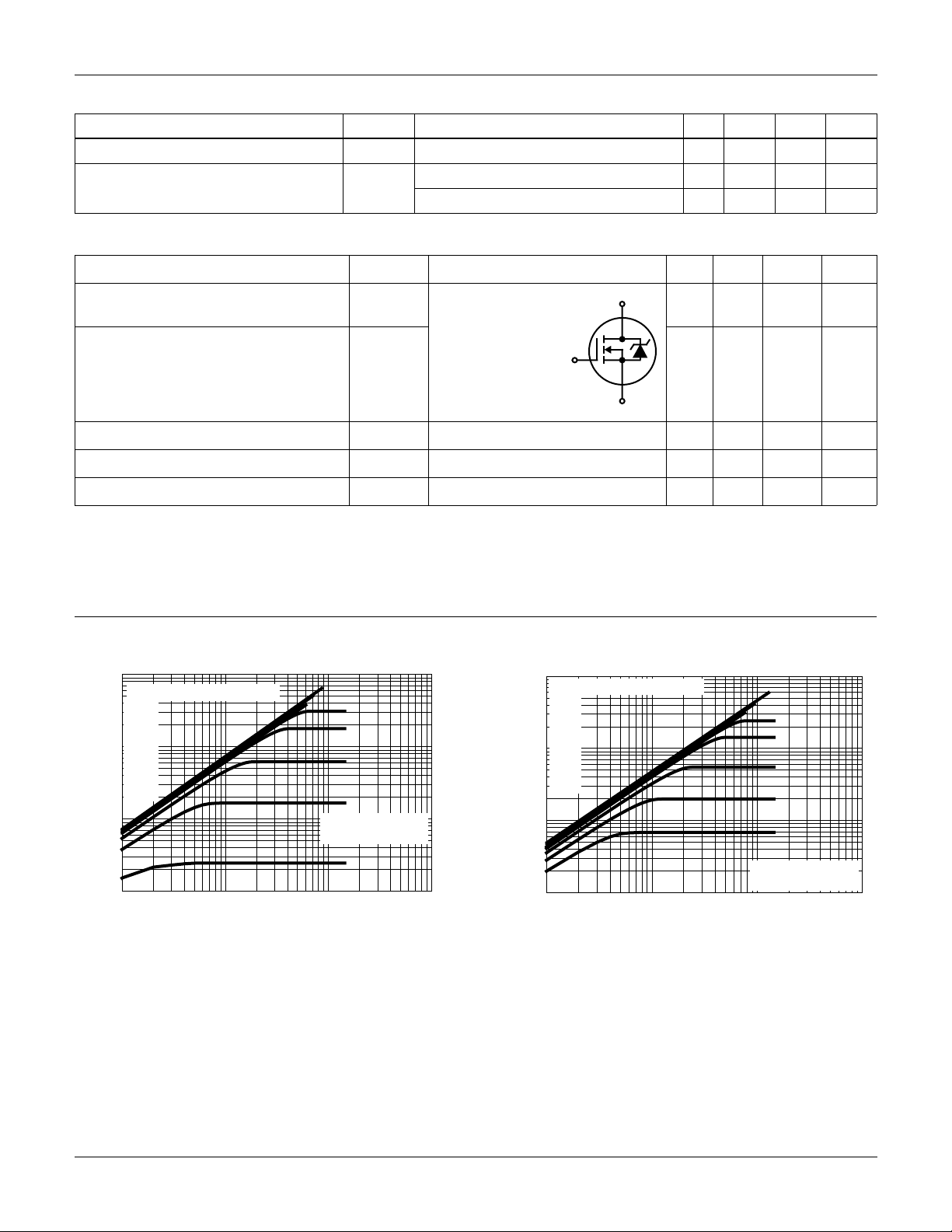
FIGURE 1. OUTPUT CHARACTERISTICS FIGURE 2. OUTPUT CHARACTERISTICS
20µs PULSE WIDTH
= 25oC
T
C
©2001 Fairchild Semiconductor Corporation HPLR3103, HPLU3103 Rev. B
 Loading...