

Fairchild Semiconductor HP4936DY Datasheet
HP4936DY
Data Sheet December 2001
5.8A, 30V, 0.037 Ohm, Dual N-Channel,
Logic Level Power MOSFET
This power MOSFET is manufactured using an innovative
process. This advanced process technology achieves the
lowest possible on-resistance per silicon area, resulting in
outstanding performance. This device is capable of
withstanding high energy in the avalanche mode and the
diode exhibits very low reverse recovery time and stored
charge. It was designed for use in applications where power
efficiency is important, such as switching regulators,
switching converters, motor drivers, relay drivers, lowvoltage bus switches, and power management in portable
and battery-operated products.
Ordering Information
PART NUMBER PACKAGE BRAND
HP4936DY SO-8 P4936DY
NOTE: When ordering, use the entire part number. Add the suffix T
to obtain the variant in tape and reel, e.g., HP4936DYT.
Features
• Logic Level Gate Drive
• 5.8A, 30V
•r
•r
• Related Literature
- TB334, “Guidelines for Soldering Surface Mount
= 0.037 Ω at I
DS(ON)
= 0.055 Ω at I
DS(ON)
Components to PC Boards”
= 5.8A, V
D
= 4.7A, V
D
GS
GS
= 10V
= 4.5V
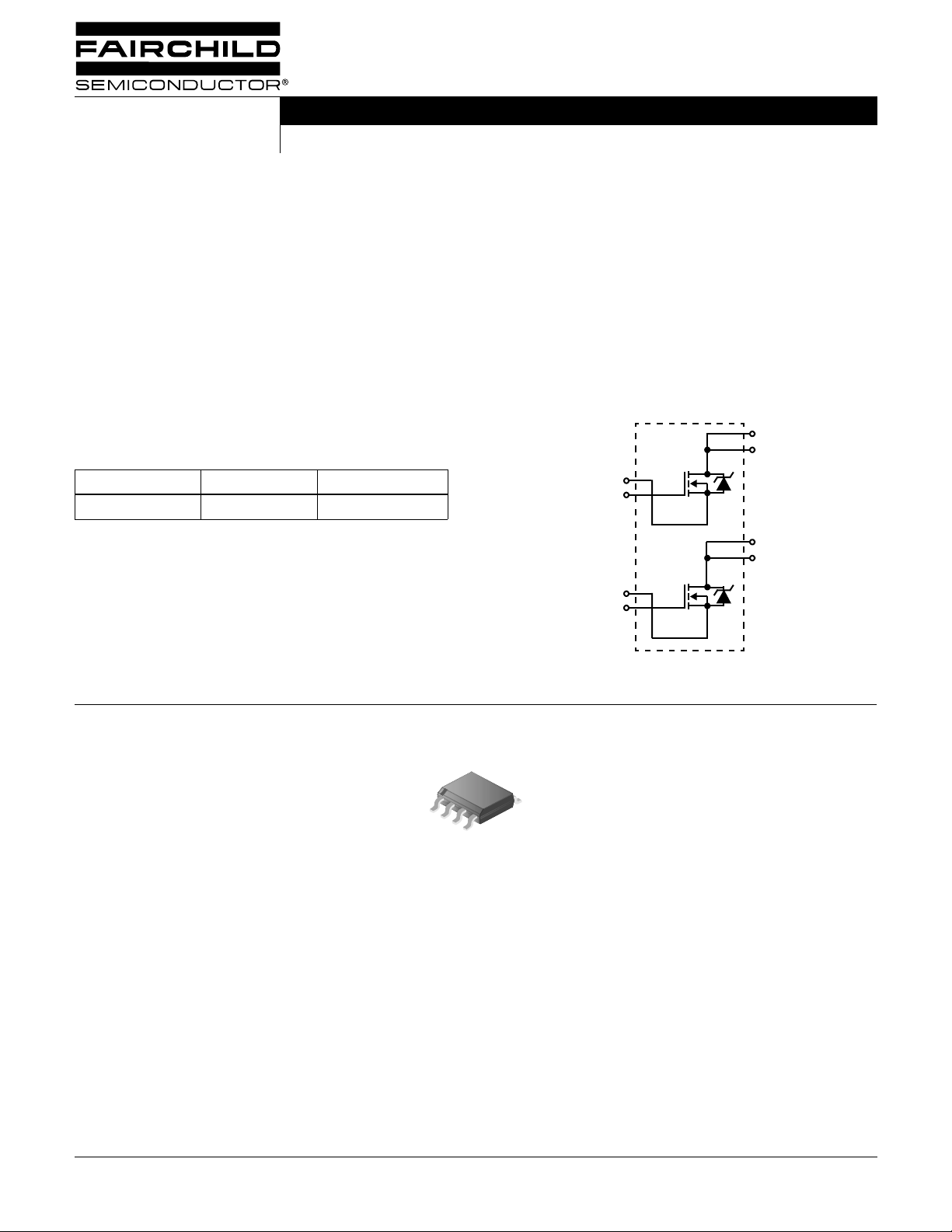
Symbol
D1(8)
D1(7)
S1(1)
G1(2)
D2(6)
D2(5)
S2(3)
G2(4)
Packaging
SO-8
©2001 Fairchild Semiconductor Corporation HP4936DY Rev. B
±
µ
Ω
Ω
≅
=
θ
HP4936DY
Absolute Maximum Ratings
o
T
= 25
C, Unless Otherwise Specified
A
HP4936DY UNITS
Drain to Source Voltage (Note 1) . . . . . . . . . . . . . . . . . . . . . . . . . . . . . . . . . . . . . . . . . . V
Drain to Gate Voltage (R
= 20k Ω ) (Note 1) . . . . . . . . . . . . . . . . . . . . . . . . . . . . . . . . V
GS
Gate to Source Voltage . . . . . . . . . . . . . . . . . . . . . . . . . . . . . . . . . . . . . . . . . . . . . . . . . . V
DSS
DGR
GS
30 V
30 V
16 V
Drain Current
Continuous . . . . . . . . . . . . . . . . . . . . . . . . . . . . . . . . . . . . . . . . . . . . . . . . . . . . . . . . . . . . I
Pulsed Drain Current (10 µ s Pulse Width) . . . . . . . . . . . . . . . . . . . . . . . . . . . . . . . . . . .I
Power Dissipation . . . . . . . . . . . . . . . . . . . . . . . . . . . . . . . . . . . . . . . . . . . . . . . . . . . . . . . P
Derate Above 25
o
C . . . . . . . . . . . . . . . . . . . . . . . . . . . . . . . . . . . . . . . . . . . . . . . . . . . . . . .
Operating and Storage Temperature . . . . . . . . . . . . . . . . . . . . . . . . . . . . . . . . . . . . T
D
DM
D
, T
J
STG
Maximum Temperature for Soldering
Leads at 0.063in (1.6mm) from Case for 10s. . . . . . . . . . . . . . . . . . . . . . . . . . . . . . . . . . T
Package Body for 10s, See Techbrief 334 . . . . . . . . . . . . . . . . . . . . . . . . . . . . . . . . . . T
CAUTION: Stresses above those listed in “Absolute Maximum Ratings” may cause permanent damage to the device. This is a stress only rating and operation of the
device at these or any other conditions above those indicated in the operational sections of this specification is not implied.
L
pkg
5.8
30
2
0.02
-55 to 150
300
260
W/
A
A
W
o
C
o
C
o
C
o
C
NOTE:
= 25
A
o
1. T
Electrical Specifications
C to 125
o
C.
o
T
= 25
C, Unless Otherwise Specified
A
PARAMETER SYMBOL TEST CONDITIONS MIN TYP MAX UNITS
Drain to Source Breakdown Voltage BV
Gate to Source Threshold Voltage V
GS(TH)
Zero Gate Voltage Drain Current I
Gate to Source Leakage Current I
Drain to Source On Resistance r
Turn-On Delay Time t
DS(ON)
d(ON)
Rise Time t
Turn-Off Delay Time t
d(OFF)
Fall Time t
Total Gate Charge Q
Gate to Source Charge Q
Gate to Drain Charge Q
Input Capacitance C
Output Capacitance C
Reverse Transfer Capacitance C
Thermal Resistance Junction to Ambient R
DSS
DSS
GSS
ISS
OSS
RSS
I
= 250 µ A, V
D
V
= V
GS
DS
V
= 30V, V
DS
V
= 30V, V
DS
V
= ± 16V - - 100 nA
GS
I
= 4.7A, V
D
I
= 5.8A, V
D
V
= 15V, I
DD
R
= 15 Ω , V
r
f
g
L
R
= 6 Ω (Figures 12, 13)
GS
V
= 15V, V
DS
(Figures 14, 15)
gs
gd
V
= 25V, V
DS
f = 1MHz
(Figure 4)
Pulse Width <10s (Figure 11)
JA
= 0V 30 - - V
GS
, I
= 250 µ A (Figure 9) 1 - - V
D
= 0V - - 1
GS
= 0V, T
GS
= 4.5V (Figures 6, 8) - 0.042 0.055
GS
= 10V (Figures 6, 8) - 0.030 0.037
GS
1A,
D
10V,
GEN
o
= 55
C--25 µ A
A
-1016ns
-1016ns
-2740ns
-2435ns
= 10V, I
GS
≅
5.8A
D
-1825nC
- 4.5 - nC
- 2.5 - nC
GS
= 0V,
- 625 - pF
- 270 - pF
-50-pF
- - 62.5
o
A
C/W
Device Mounted on FR-4 Material
Source to Drain Diode Specifications
PARAMETER SYMBOL TEST CONDITIONS MIN TYP MAX UNITS
Source to Drain Diode Voltage V
SD
Reverse Recovery Time t
©2001 Fairchild Semiconductor Corporation HP4936DY Rev. B
I
= 1.7A (Figure 7) - 0.8 1.2 V
SD
I
rr
= 1.7A, dI
SD
/dt = 100A/ µ s - 45 80 ns
SD
 Loading...