

Fairchild Semiconductor HGTP14N37G3VL, HGT1S14N37G3VLS Datasheet
HGT1S14N37G3VLS, HGTP14N37G3VL
Data Sheet December 2001
14A, 370V N-Channel, Logic Level, Voltage
Clamping IGBTs
This N-Channel IGBT is a MOS gated, logic level device
which is intended to be used as an ignition coil driver in
automotive ig nition circuits. Unique features in clude an
active voltage clamp between the collector and the gate
which provide s Self Clamped Inductive Switching (SCIS)
capability in ignition circuits. Internal diodes provide ESD
protection for the logic level gate. Both a series resistor and
a shunt resister are provided in the gate circuit.
Formerly Developmental Type TA49169.
Ordering Information
PART NUMBER PACKAGE BRAND
HGT1S14N37G3VLS TO-263AB 14N37GVL
HGTP14N37G3VL TO-220AB 14N37GVL
NOTE: When ordering, use the entire part number. Add the suffix 9A
to obtain the TO-263AB in tape and reel, i.e. HGT1S14N37G3VLS9A
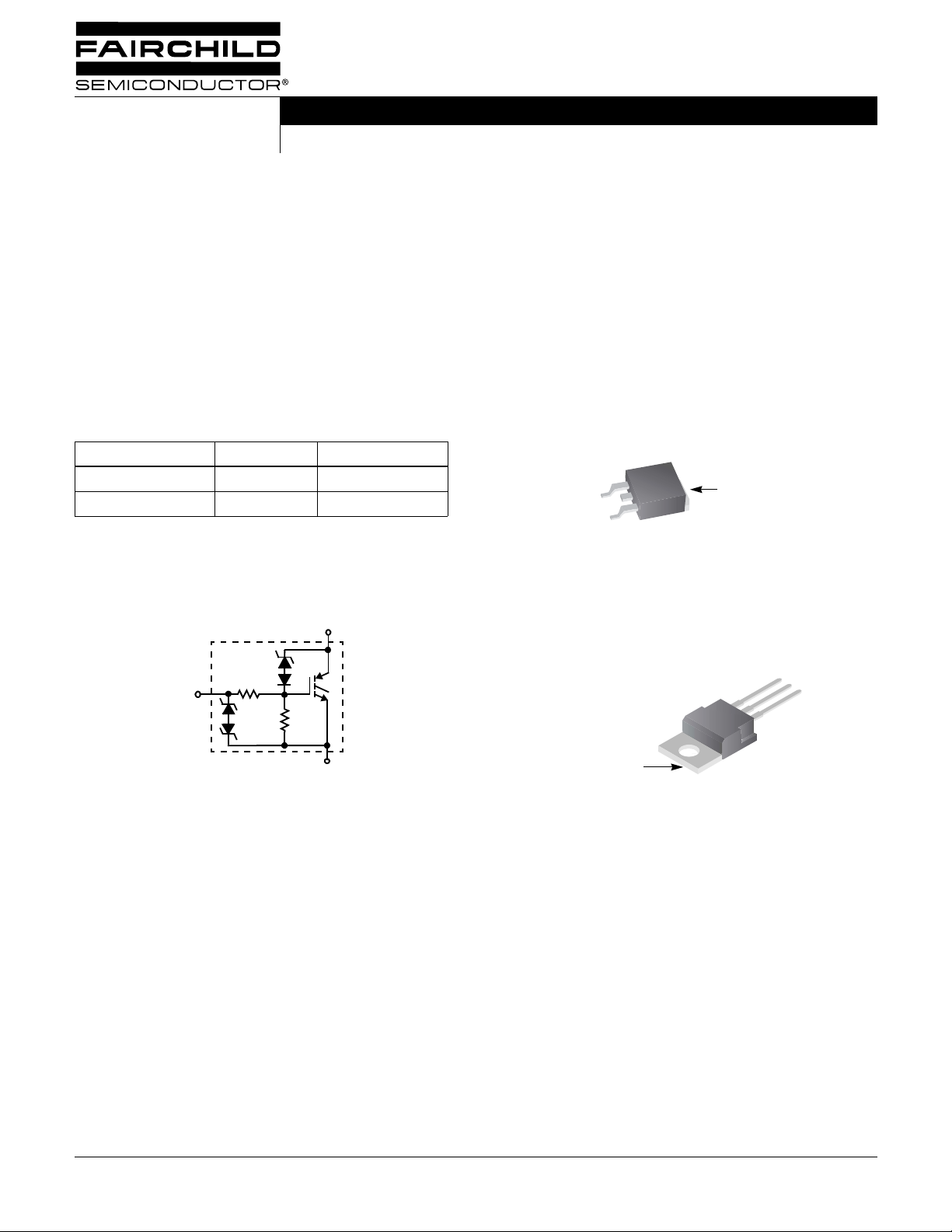
Symbol
COLLECTOR
Features
• Logic Level Gate Drive
• Internal Voltage Clamp
• ESD Gate Protection
•T
= 175oC
J
• Internal Series and Shunt Gate Resistors
• Low Conduction Loss
• Ignition Energy Capable
Packaging
JEDEC TO-263AB
COLLECTOR
G
E
JEDEC TO-220AB
(FLANGE)
E
R
GATE
Fairchild CORPORATION IGBT PRODUCT IS COVE RED BY ONE OR MORE OF THE FOLLOWING U.S. PATENTS
4,364,073 4,417,385 4,430,792 4,443,931 4,466,176 4,516,143 4,532,534 4,587,713
4,598,461 4,605,948 4,620,211 4,631,564 4,639,754 4,639,762 4,641,162 4,644,637
4,682,195 4,684,413 4,694,313 4,717,679 4,743,952 4,783,690 4,794,432 4,801,986
4,803,533 4,809,045 4,809,047 4,810,665 4,823,176 4,837,606 4,860,080 4,883,767
4,888,627 4,890,143 4,901,127 4,904,609 4,933,740 4,963,951 4,969,027
1
R
2
COLLECTOR
EMITTER
(FLANGE)
C
G
©2001 Fairchild Semiconductor Corpo ration HGT1S14N37G3VLS, HGTP14N37G3VL Rev. B
HGT1S14N37G3VLS, HGTP14N37G3VL
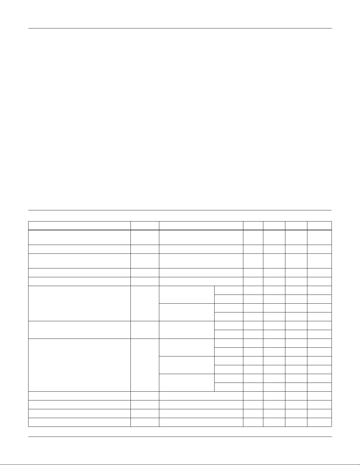
Absolute Maximum Ratings
TC = 25oC, Unless Otherwise Specified
HGT1S14N37G3VLS,
HGTP14N37G3VL UNITS
Collector to Emitter Breakdown Voltage at 10mA . . . . . . . . . . . . . . . . . . . . . . . . . . . . .BV
Emitter to Collector Breakdown Voltage at 10mA . . . . . . . . . . . . . . . . . . . . . . . . . . . . .BV
Collector Current Continuous at V
= 5V, TC = 25oC . . . . . . . . . . . . . . . . . . . . . . . . . . . I
GE
at VGE = 5V, TC = 110oC . . . . . . . . . . . . . . . . . . . . . . . . I
Gate to Emitter Voltage (Note 1) . . . . . . . . . . . . . . . . . . . . . . . . . . . . . . . . . . . . . . . . . . . V
Inductive Switching Current at L = 3mH, T
at L = 3mH, T
Collector to Emitter Avalanche Energy at L = 3 mH, T
Pow er Dissi pation Total at T
Power Dissipation Derating T
= 25oC . . . . . . . . . . . . . . . . . . . . . . . . . . . . . . . . . . . . . . . . . P
C
> 25oC . . . . . . . . . . . . . . . . . . . . . . . . . . . . . . . . . . . . . . . . . . 0.91 W/oC
C
= 25oC . . . . . . . . . . . . . . . . . . . . . . . . . . . . I
C
= 150oC. . . . . . . . . . . . . . . . . . . . . . . . . . . I
C
= 25oC . . . . . . . . . . . . . . . . . . . . E
C
Storage Junction Temperature Range . . . . . . . . . . . . . . . . . . . . . . . . . . . . . . . . . . . . . . . T
CER
ECS
C25
C110
GEM
SCIS
SCIS
STG
Operating Junction Temperature Range . . . . . . . . . . . . . . . . . . . . . . . . . . . . . . . . . . . . . . . T
AS
D
J
380 V
24 V
25 A
18 A
±10 V
15 A
11.5 A
340 mJ
136 W
-55 to 175
-55 to 175
o
C
o
C
Electrostatic Voltage HBM at 250pF, 1500Ω All Pin Configurations. . . . . . . . . . . . . . . . . .ESD 5 kV
Electrostatic Voltage MM at 200pF, 0Ω All Pin Configurations. . . . . . . . . . . . . . . . . . . . . . ESD 2 kV
Maximum Lead T emperature f or Soldering
Leads at 0.063in (1.6mm) from Case for 10s. . . . . . . . . . . . . . . . . . . . . . . . . . . . . . . . . . T
Package Body for 10s, See Techbrief 334 . . . . . . . . . . . . . . . . . . . . . . . . . . . . . . . . . . T
CAUTION: Stresses above those listed in “A bsolute Maximu m Rating s” may cause per manent d amage to t he device. This is a str ess on ly rating and operation o f the
device at these or any other conditions above those indicated in the operational sections of this specification is not implied.
L
PKG
300
260
o
C
o
C
NOTE:
1. May be exceeded if I
is limited to 10mA.
GEM
Electrical Specifications
TJ = 25oC, Unless Otherwise Specified
PARAMETER SYMBOL TEST CONDITIONS MIN TYP MAX UNITS
Collector to Emitter Breakdown Voltage BV
Gate to Emitter Plateau Voltage V
Gate Charge Q
Collector to Emitter Clamp Breakdown Voltage BV
Emitter to Collector Breakdown Voltage BV
Collector to Emitter Leakage Current I
Emitter to Collector Leakage Current
Collector to Emitter On-State Voltage V
Gate to Emitter Threshold Voltage V
Gate Series Resistance R
Gate to Emitter Resistance R
Gate to Emitter Leakage Current I
CERIC
GEPIC
G(ON)IC
CE(CL)IC
ECSIC
CES
I
ECS
CE(ON)IC
GE(TH)IC
1
2
GES
= 10mA, RG = 1kΩ, VGE = 0V,
= -55oC to 175oC (Figure 16)
T
J
320 350 380 V
= 6.5A, VCE = 12V - 2.76 - V
= 6.5A, VCE = 12V, VGE = 5V
-27 - nC
(Figure 16)
= 15A, RG = 1kΩ 320 350 380 V
= 10mA 24 28 - V
VCE = 300V, VGE = 0V
(Figure 13)
V
= 250V,
CE
V
= 0V (Figure 13)
GE
VEC = -24V,
V
= 0V (Figure 13)
GE
= 6A, VGE = 4.0V
(Figures 3 through 9)
I
= 10A, VGE = 4.5V
C
(Figures 3 through 9)
I
= 14A, VGE = 5V
C
(Figures 3 through 9)
TJ = 25oC- - 40 µA
T
= 175oC - - 250 µA
J
= 25oC- - 10 µA
T
J
T
= 175oC- - 75 µA
J
= 25oC- - 10 mA
T
J
T
= 175oC- - 50 mA
J
TJ = -55oC- 1.31.45 V
T
= 25oC - 1.25 1.6 V
J
TJ = 25oC - 1.45 1.75 V
T
= 175oC- 1.5 1.9 V
J
TJ = 25oC- 1.6 2 V
T
= 175oC- 1.7 2.3 V
J
= 1mA, VCE = VGE (Figure 12) 1.3 1.8 2.2 V
- 70 150 Ω
10 18 26 kΩ
VGE = ±10V ±310 ±500 ±1000 µA
©2001 Fairchild Semiconductor Corpo ration HGT1S14N37G3VLS, HGTP14N37G3VL Rev. B
 Loading...