

Fairchild Semiconductor FSTD32211 Datasheet
FSTD32211
40/48-Bit Bus Switch with Level Shifting
FSTD32211 40/48-Bit Bus Switch with Level Shifting
September 2001
Revised July 2002
General Description
The Fairchild Switch FSTD32211 provides up to 48-bits of
high-speed CMOS TTL- compatible bu s switching. T he low
on resistance of the switch allows inputs to be connected to
outputs without adding propagation delay or generating
additional ground b ounce noise. A diode to V
integrated into the circuit to allow for leve l shifting b etween
5V inputs and 3.3V outputs.
The device can be organize d as four 12-bit, two 24-bit, or
one 48-bit bus swit ch. When routed as a 40-bi t bu s sw it ch,
the device can be orga nized as four 10-bit, two 20 -bit or
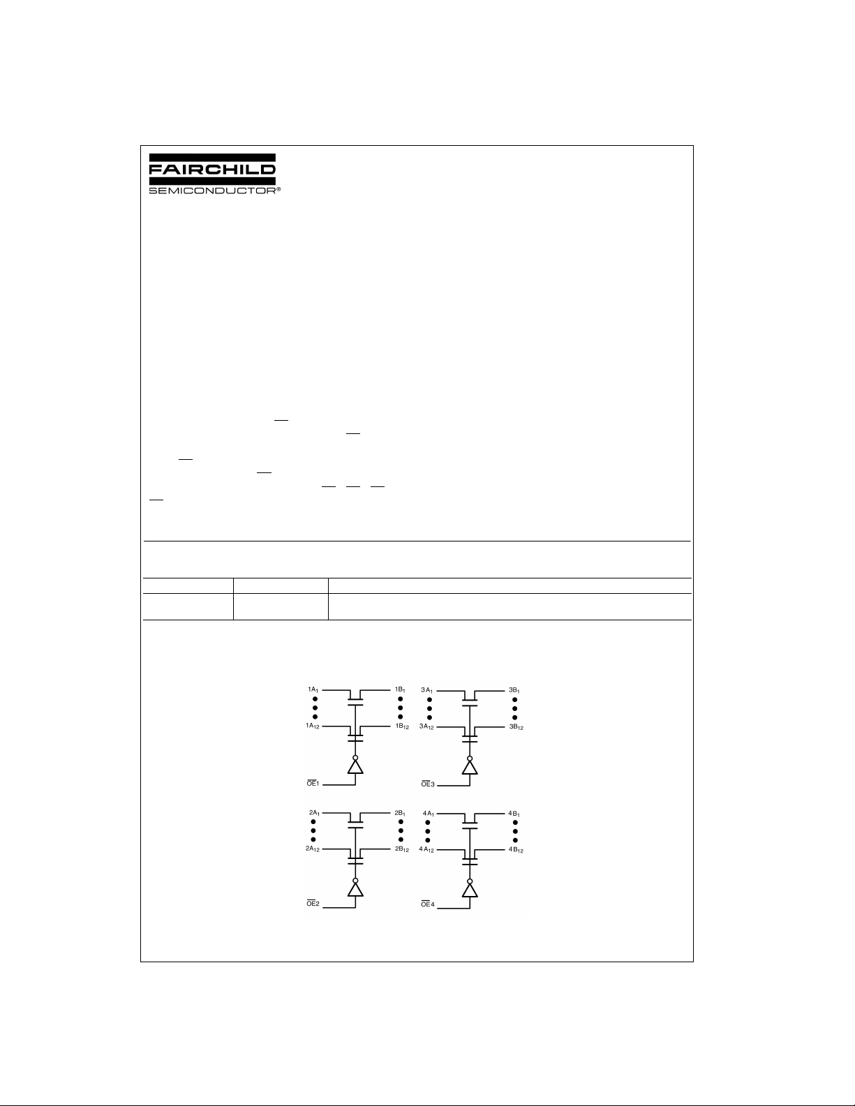
one 40-bit bus switch. When OE
and Port 1A is connected to Por t 1B. When OE
the switch is ON and Port 2A is connected to Port 2B.
When OE
nected to Port 3B. When OE
Port 4A is connected to Port 4B. When OE
OE
A and B Ports.
is LOW, the switch is ON and Port 3A is con-
3
are HIGH, a hig h im pe dan ce state exists betw ee n t he
4
is LOW, the switch is ON
1
is LOW, the switch is ON and
4
has been
CC
is LOW,
2
, OE2, OE3, or
1
Features
■ 4Ω switch connection between two ports
■ Voltage level shifting
■ Minimal propagation delay through the switch
■ Low l
CC
■ Zero bounce in flow-through mode
■ Control inputs compatible with TTL level
■ Packaged in plastic Fine-Pitch Ball Grid Array (FBGA)
Ordering Code:
Order Number Package Number Package Description
FSTD32211G
(Note 1)(Note 2)
Note 1: Ordering code “G” indicates Trays.
Note 2: Devices also available in Tape and Reel. Specify by appending th e s uffix let t er “X” to the ordering code.
BGA114A 114-Ball Fine-Pitch Ball Grid Array (FBGA), JEDEC MO-205, 5.5mm Wide
Logic Diagram
© 2002 Fairchild Semiconductor Corporation DS500378 www.fairchildsemi.com
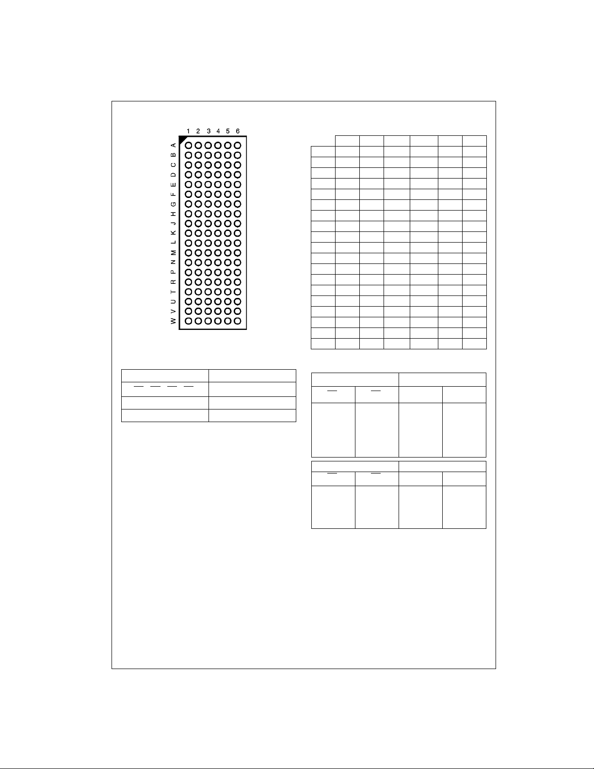
Connection Diagram
FSTD32211
(Top Thru View)
Pin Descriptions
Pin Name Description
OE
, OE2, OE3, OE
1
1A, 2A, 3A, 4A Bus A
1B, 2B, 3B, 4B Bus B
FBGA Pin Assignments
(40-Bit Routing)
123 4 56
A 1A
B 1A41A3GND OE11B31B
C 1A61A5GND GND 1B51B
D 1A81A7GND GND 1B71B
E 1A101A9V
F 2A22A1V
G 2A42A3V
H 2A62A5GND GND 2B52B
J 2A82A72A92B92B72B
K 2A103A10GND GND 3B102B
L 3A93A8GND GND 3B83B
M 3A73A6GND V
N 3A53A4V
P 3A33A2V
R 3A14A10GND GND 4B103B
T 4A94A8GND GND 4B84B
U 4A74A6GND 4B14B64B
V 4A54A44A1OE44B44B
W 4A34A2OE
1A1NC OE21B11B
2
CCVCC
CCVCC
GND 2B32B
CC
CC
CCVCC
CCVCC
NC 4B24B
3
1B91B
2B12B
3B63B
3B43B
3B23B
2
4
6
8
10
2
4
6
8
10
9
7
5
3
1
9
7
5
3
Truth Tables
Inputs Inputs/Outputs
Bus Switch Enables
4
OE
1
LL1A = 1B 2A = 2B
LH1A = 1B Z
HLZ2A
HHZZ
OE
3
LL3A
LH3A
HLZ4A
HHZZ
OE
2
1A, 1B 2A, 2B
Inputs Inputs/Outputs
OE
4
3A, 3B 4A, 4B
= 3B 4A = 4B
= 3B Z
= 2B
= 4B
www.fairchildsemi.com 2
Connection Diagram
(Top Thru View)
Pin Descriptions
Pin Name Description
OE
, OE2, OE3, OE
1
1A, 2A, 3A, 4A Bus A
1B, 2B, 3B, 4B Bus B
4
Bus Switch Enables
FBGA Pin Assignments
(48-Bit Routing)
123 4 56
A 1A
1A1NC OE21B11B
2
B 1A41A31A7OE11B31B
C 1A61A5GND 1B71B51B
D 1A101A91A81B81B91B
E 1A121A112A12B11B111B
F 2A42A32A22B22B32B
G 2A62A5V
GND 2B52B
CC
H 2A82A7GND GND 2B72B
J 2A102A92A112B
11
2B92B
K 2A123A12GND GND 3B122B
L 3A113A10GND GND 3B103B
M 3A93A8GND V
CC
3B83B
N 3A73A63A23B23B63B
P 3A53A43A13B13B43B
R 3A34A124A84B84B123B
T 4A114A104A74B74B104B
U 4A94A6GND 4B14B64B
V 4A54A44A1OE44B44B
W 4A34A2OE3NC 4B24B
Truth Tables
Inputs Inputs/Outputs
OE
1
OE
2
LL1A
LH1A = 1B Z
HLZ2A
HHZZ
Inputs Inputs/Outputs
OE
3
OE
4
LL3A
LH3A
HLZ4A
HHZZ
1A, 1B 2A, 2B
= 1B 2A = 2B
3A, 3B 4A, 4B
= 3B 4A = 4B
= 3B Z
FSTD32211
2
4
6
10
12
4
6
8
10
12
11
9
7
5
3
11
9
5
3
= 2B
= 4B
3 www.fairchildsemi.com
 Loading...