

Fairchild Semiconductor FSTD16861 Datasheet
FSTD16861
20-Bit Bus Switch with Level Shifting
FSTD16861 20-Bit Bus Switch with Level Shifting
May 2001
Revised May 2001
General Description
The Fairchild Switc h FSTD16861 provides 20-bi ts of highspeed CMOS TTL-compatible bus switching. The low On
Resistance of the switch allows inputs to be connected to
outputs without adding propagation delay or generating
additional ground b ounce noise. A diode to V
integrated into the circuit to allow for leve l shifting b etween
5V inputs and 3.3V outputs.
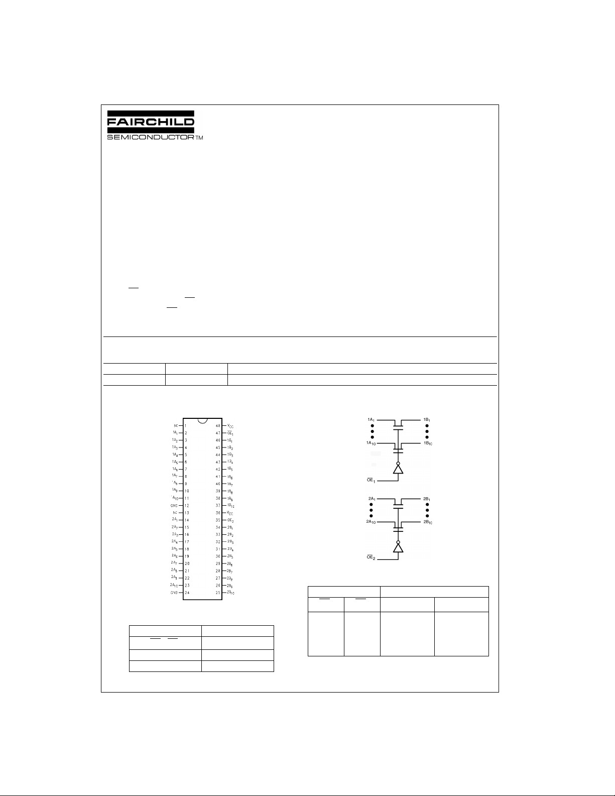
The device is organ ized as a 10-bit or 20-bit b us switch.
When OE
nected to Port 1B. When OE
to Port 2B. When OE
exists between the A and B Ports.
is LOW, the switch is ON and Port 1A is con-
1
is LOW, Port 2A is connected
2
is HIGH, a high imped ance state
X
has been
CC
Features
■ 4Ω switch connection between two ports.
■ Minimal propagation delay through the switch.
■ Low l
■ Zero bounce in flow-through mode.
■ Control inputs compatible with TTL level.
■ TruTranslation
.
CC
3.3V outputs
voltage translation from 5.0V inp uts to
Ordering Code:
Order Number Package Number Package Description
FSTD16861MTD MTD48 48-Lead Thin Shrink Small Outline Package (TSSOP), JEDEC MO-153, 6.1mm Wide
Devices also availab le in Tape and Reel. Specify by appending the suffix letter “X” to the o rdering code.
Connection Diagram
Logic Diagram
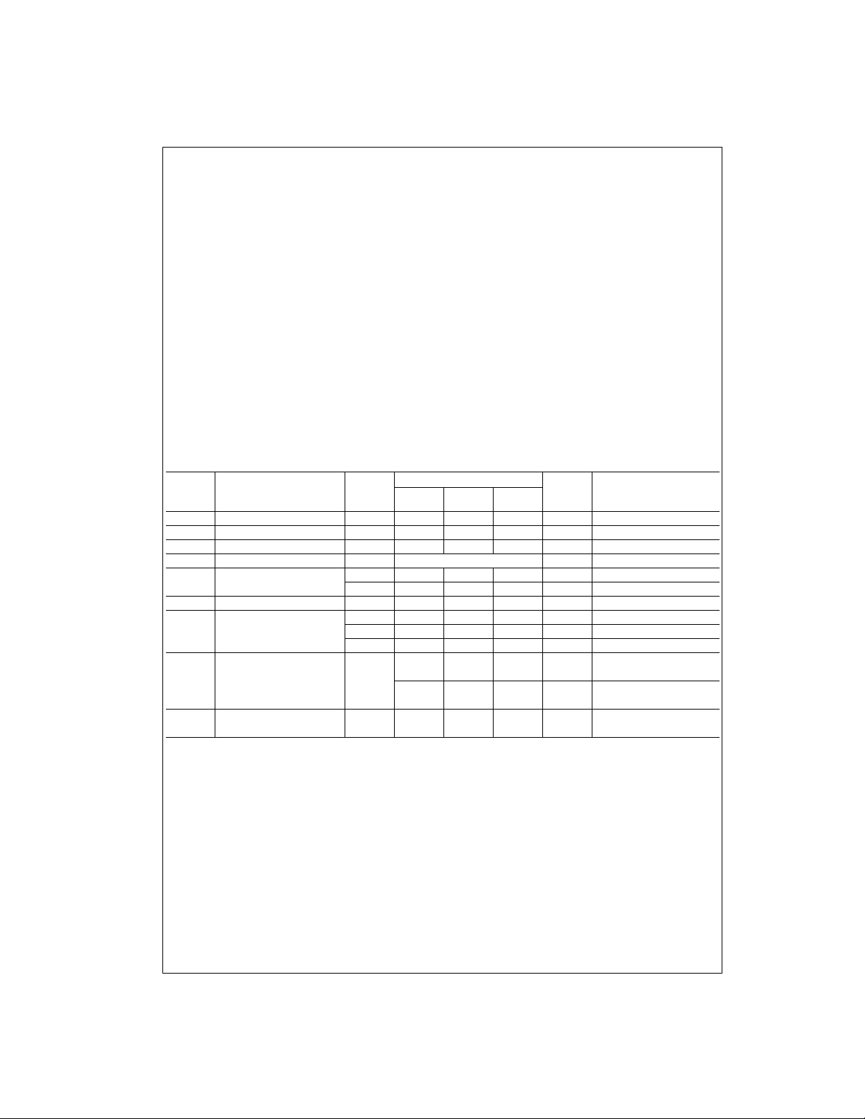
Truth Table
Inputs Inputs/Outputs
OE
Pin Descriptions
Pin Name Description
OE
, OE
1
, 2A
1A
n
n
1B
, 2B
n
n
TruTranslation is trademark of Fairch ild Semiconductor Corporation.
© 2001 Fairchild Semiconductor Corporation DS500421 www.fairchildsemi.com
2
Bus Switch Enables
Bus A
Bus B
LL1A
LH1A
HL Z 2A
HH Z Z
H = HIGH Voltage Level
L = LOW Voltage Level
Z = High Impedance
OE
1
2
1A, 1B 2A, 2B
= 1B 2A = 2B
= 1B Z
= 2B
Absolute Maximum Ratings(Note 1) Recommended Operating
Supply Voltage (VCC) −0.5V to +7.0V
DC Switch Voltage (V
DC Input Voltage (V
FSTD16861
DC Input Diode Current (l
DC Output Current (I
DC V
/GND Current (ICC/I
CC
Storage Temperature Range (T
) (Note 2) −0.5V to +7.0V
S
) (Note 3) −0.5V to +7.0V
IN
) V
< 0V −50 mA
IK
IN
) 128 mA
OUT
) ±100 mA
GND
) −65°C to +150 °C
STG
Conditions
Power Supply Operating (V
Input Voltage (V
Output Voltage (V
Input Rise and Fall Time (t
Switch Control Input 0 ns/V to 5 ns/V
Switch I/O 0 ns/V to DC
Free Air Operating Temperature (T
Note 1: The “Absolute Maximum Ratings” are those values bey ond which
the safety of the d evice cannot be guaranteed. The device sh ould not be
operated at these limit s. The parametric values defin ed in the Electrical
Characteristics tables are not guaranteed at the absolute maximum rating.
The “Recomme nded O peratin g Cond itions ” table will defin e the condition s
for actual device operation.
is the voltage observed/applied at either the A or B Ports across
Note 2: V
S
the switch.
Note 3: The input and output ne gative vo ltage ra tings may be excee ded if
the input and output diode current ratings are observed.
Note 4: Unused control inputs must be held HIGH or LOW. They may not
float.
(Note 4)
CC)
)0V to 5.5V
IN
)0V to 5.5V
OUT
, tf)
r
)-40 °C to +85 °C
A
DC Electrical Characteristics
V
Symbol Parameter
V
IK
V
IH
V
IL
V
OH
I
I
I
OZ
R
ON
I
CC
∆ I
Note 5: Typi c al values are at VCC = 5.0V and TA = +25°C
Note 6: Measured by the volta ge drop between A an d B pins at the indicated c urrent through the switch. On Resistance is determined by the lower of the
voltages on the two (A or B) pins.
Clamp Diode Voltage 4.5 −1.2 V IIN = −18 mA
HIGH Level Input Voltage 4.5-5.5 2.0 V
LOW Level Input Voltage 4.5-5.5 0.8 V
HIGH Level 4.5-5.5 See Figure 3 V
Input Leakage Current 5.5 ±1.0 µA0 ≤ VIN ≤ 5.5V
OFF-STATE Leakage Current 5.5 ±1.0 µA0 ≤ A, B ≤ V
Switch On Resistance 4.5 4 7 Ω VIN = 0V, IIN = 64 mA
(Note 6) 4.5 4 7 Ω V
Quiescent Supply Current
Increase in I
CC
per Input 5.5 2.5 mA One Input at 3.4V
CC
CC
(V) Min Typ
010µAV
4.5 35 50 Ω VIN = 2.4V, IIN = 15 mA
5.5
TA = −40 °C to +85 °C
(Note 5)
Max
1.5 mA
10 µA
Units Conditions
= 5.5V
IN
CC
= 0V, IIN = 30 mA
IN
OE1 = OE2 = GND
= VCC or GND, I
V
IN
OE1 = OE2 = V
VIN = VCC or GND, I
Other Inputs at VCC or GND
4.5V to 5.5V
= 0
OUT
CC
= 0
OUT
www.fairchildsemi.com 2
 Loading...