

Fairchild Semiconductor FSTD16450 Datasheet
FSTD16450
Configurable 4-Bit to 20-Bit Bus Switch
with Selectable Level Shifting
FSTD16450 Configurable 4-Bit to 20-Bit Bus Switch with Selectable Level Shifting
January 2001
Revised August 2001
General Description
The Fairchild Univers al Bus Switch FSTD16450 provides
4-bit, 5-bit, 8-bi t, 10-b it, 16- bit, 20 -bit of hig h-s peed CMOS
TTL-compatible bus switching. The low on resistance of
the switch allows inputs to be conn ecte d to ou tpu ts witho ut
adding propagation de lay or generating additi onal ground
bounce noise.
The FSTD16450 is designed to allow “customer” configuration control of the enable co nnections . The device is o rganized as either a 4-bit, 5-bit , 10-bi t or 20-b it bus swit ch. 8bit and 16-bit configurations are also achievable (see Functional Description). The d evice' s bi t con figur atio n i s chos en
through select pin logic. (s ee Truth Table). When OE
LOW, Port A
the switch is OPEN.
Another key device feature is the addition of a level shifting
select pin, “S
standard N-MOS switch. When S
is integrated into the circuit allowing for level shifting
between 5V inputs and 3.3V outputs.
is connected to Port Bx. When OEx is HIGH,
x
”. When S2 is LOW, the device behaves as a
2
is HIGH, a diode to V
2
Features
■ 4Ω switch connection between two ports
■ Voltage level shifting
■ Minimal propagation delay through the switch
■ Low l
CC
■ Zero bounce in flow-through mode
■ Control inputs compatible with TTL level
■ Also packaged in plastic Fine-Pitch Ball Grid Array
(FBGA) (Preliminary)
Applications Note
is
x
Select pins S0, S1, S2 are intended to be used as static
user configurable control pins. The AC performance of
these pins has not be en characterized or teste d. Swit ching
of these select pin s during system operation may temporarily disrupt output logic states and/or enable pin controls.
CC
Ordering Code:
Order Number Package Number Package Description
FSTD16450GX
(Note 1)
FSTD16450MTD MTD56 56-Lead Thin Shrink Small Outline Package (TSSOP), JEDEC MO-153, 6.1mm Wide
Devices also availab l e in Tape and Reel. Specify by appending th e s uffix let t er “X” to the ordering code.
Note 1: BGA package available in Tape and Reel only.
BGA54A
(Preliminary)
54-Ball Fine-Pitch Ball Grid Array (FBGA), JEDEC MO-205, 5.5mm Wide
[Tape and Reel]
UHC is a trademark of Fairchild Semiconductor Corporation.
© 2001 Fairchild Semiconductor Corporation DS500438 www.fairchildsemi.com
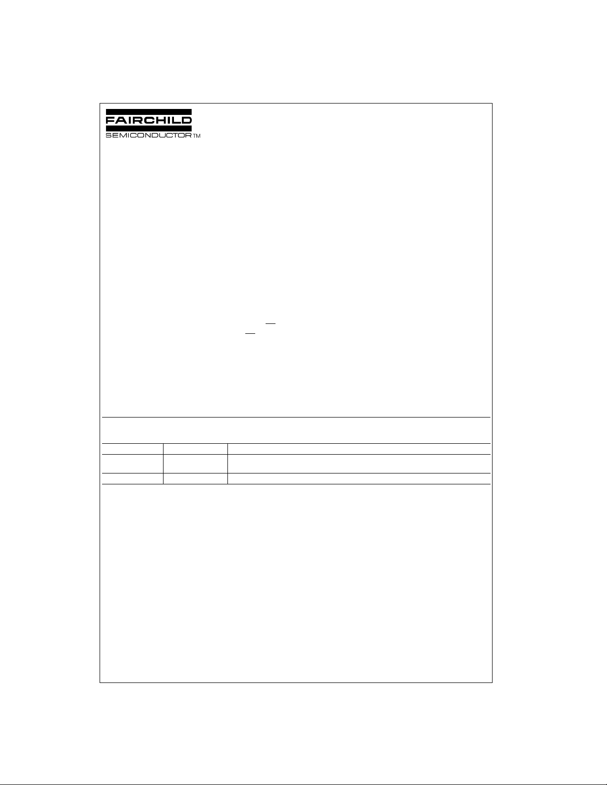
Connection Diagrams
Pin Assignments for TS SO P
FSTD16450
Pin Descriptions
Pin Name Description
OE
, OE
1
2
Bus Switch Enables
1A, 2A Bus A
1B, 2B Bus B
S
, S
0
1
S
2
Bit Configuration Enables
Level Shifting Diode Enable
FBGA Pin Assignments
123456
A 1A
B 1A51A41A11B11B41B
C 1A71A6GND OE51B61B
D 1A91A8GND V
E 2A11A
F 2A32A2S
G 2A52A4VCCGND 2B42B
H 2A72A62A102B102B62B
J 2A92A8OE4OE32B82B
1A2OE1OE21B21B
3
CC
10S0VCC1B10
S22B22B
1
1B81B
2B
3
5
7
9
1
3
5
7
9
Pin Assignments for FBGA
(Top Thru View)
www.fairchildsemi.com 2
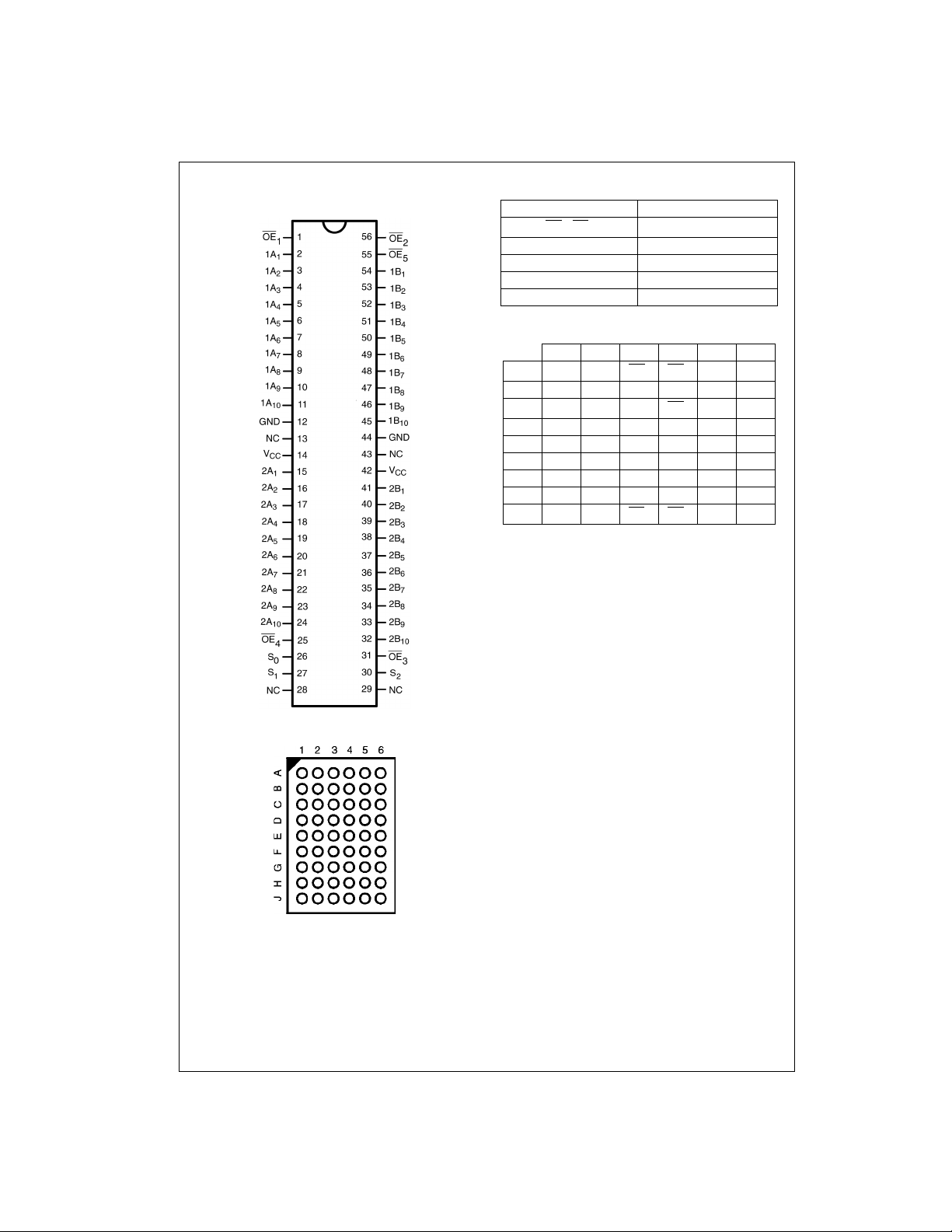
Logic Diagrams
20-Bit Configuration
(Configuration 1)
FSTD16450
10-Bit Configuration
(Configuration 2)
5-Bit Configuration
(Configuration 3)
4-Bit Configuration
(Configuration 4)
3 www.fairchildsemi.com
Functional Description
The device can a lso be configured as an 8 and 16-bit devi ce by grounding the u nused pins in Configu rations 2 and 1
respectively. The 8-bit configuration may also be achieved by tying two of the 4-bit enables from configuration together and
tying the remaining enabl e pin (OE
FSTD16450
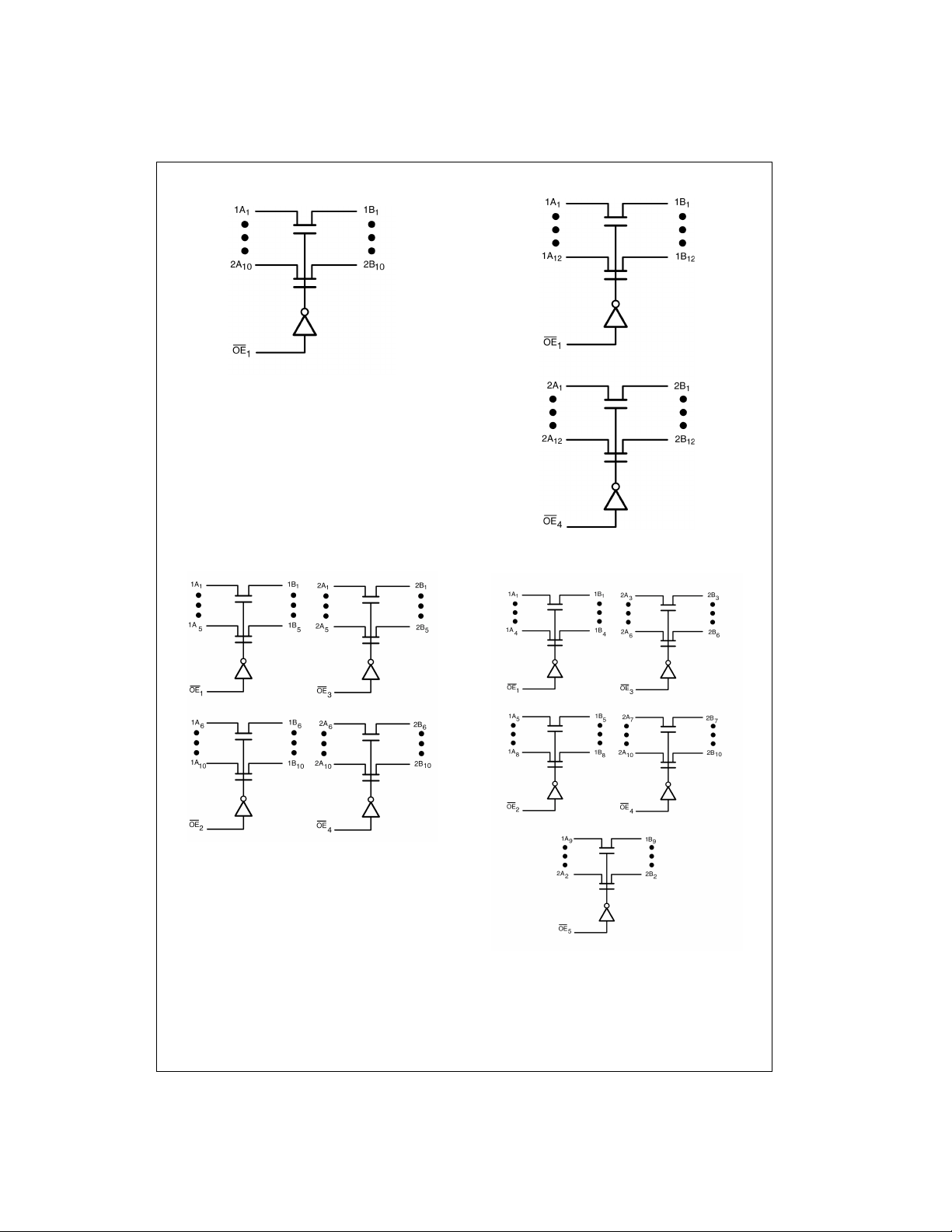
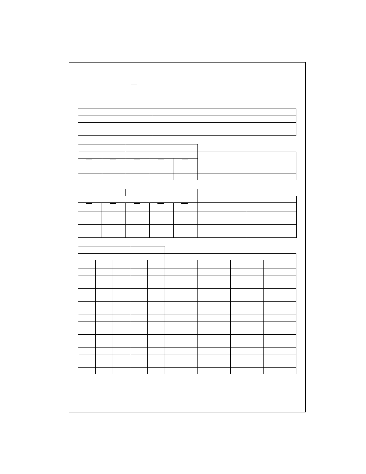
Truth Tables (X = V
(see Functional Description)
S
2
L Std. NMOS Switch
H Level Shifting Diode Enabled
Configuration 1
OE
OE
1
2
LXXXX 1A
HXXXX Z
Configuration 2
OE
OE
1
2
LXXLX 1A
LXXHX 1A
HXXLX Z 2A
HXXHX Z Z
) HIGH.
or GND)
CC
Select Pin
Mode
= S1 = L
Inputs
OE
3
S
0
OE
S
= L, S1 = H
0
OE
4
5
20-Bit Configuration
Inputs/Outputs
= 1B
1-10
1-10
10-Bit Configuration
Inputs Inputs/Outputs
OE
OE
3
4
OE
1A
5
1-10
= 1B
= 1B
X
= 1B
X
1-10
X
X
, 2A
1-10
= 2B
2A
1-10
2AX = 2B
1-10
= 2B
= 2B
X
Z
1-10
X
X
S
Configuration 3
= H, S1 = L
0
5-Bit Configuration
Inputs Inputs/Outputs
OE
OE2OE3OE4OE51A
1
LLLLX1A
LLLHX1A
LLHLX1A
LLHHX1A
LHLLX1A
LHLHX1A
LHHLX1A
LHHHX1A
HLLLX Z 1A
HLLHX Z 1A
HLHLX Z 1A
HLHHX Z 1A
HHL LX Z Z 2A
HHLHX Z Z 2A
1-5
, 1B
= 1B
x
= 1B
x
= 1B
x
= 1B
x
= 1B
x
= 1B
x
= 1B
x
= 1B
x
1-5
1A
, 1B
6-10
1Ay = 1B
x
1Ay = 1B
x
1Ay = 1B
x
1Ay = 1B
x
x
x
x
x
Z2A
Z2A
ZZ2A
ZZZ
= 1B
y
= 1B
y
= 1B
y
= 1B
y
6-10
y
y
y
y
y
y
y
y
2A
, 2B
1-5
1-5
2Ax = 2B
x
2Ax = 2B
x
Z2A
ZZ
= 2B
x
x
= 2B
x
x
2Ax = 2B
x
2Ax = 2B
x
Z2A
ZZ
= 2B
x
x
= 2B
x
x
HHHLX Z Z Z 2A
HHHHX Z Z Z Z
www.fairchildsemi.com 4
2A
6-10
2Ay = 2B
2Ay = 2B
2Ay = 2B
2Ay = 2B
, 2B
Z
= 2B
y
Z
= 2B
y
Z
= 2B
y
Z
= 2B
y
6-10
y
y
y
y
y
y
y
y
 Loading...